Embed Size (px)
Citation preview

Progress In Electromagnetics Research B, Vol. 16, 209–228, 2009
FRACTAL ANTENNA FOR PASSIVE UHF RFIDAPPLICATIONS
S. H. Zainud-Deen, H. A. Malhat, and K. H. Awadalla
Faculty of Electronic EngineeringMenoufia UniversityEgypt
Abstract—This paper addresses the design of fractal antennas placedonto dielectric object in the UHF RFID band and introduces a tagantenna configuration of simple geometry having impedance tuningcapability. Through the paper, the dimensions of the fractal antennaare optimized to improve the impedance matching with the chipimpedance. The tag performance changes are studied when it is placedon different objects (e.g., cardboard boxes with various content), orwhen other objects are present in the vicinity of the tagged object.It has been shown that a tag antenna can be designed or tuned foroptimum performance on a particular object. Using the finite elementmethod the open circuit voltage and the polarization mismatch factoragainst the operating frequency are calculated. The input impedance,reflection coefficient, power transmission coefficient and the read rangeas a function of frequency are illustrated. The performance of thetag antenna in the presence of the dielectric box and different objectmaterials inside the box is illustrated. The effect of the objects thatare placed in the center of the dielectric box didn’t have a significanteffect on the performance of the tag antenna; there is a small shift inthe resonance frequency but still within the operating frequency band.Both the power transmission coefficient and the read range changewith the object material. The backscattering properties of the tagantenna have been studied. The differential radar cross-section of thetag antenna is calculated for different antenna loads.
Corresponding author: H. A. Malhat (er [email protected]).
210 Zainud-Deen, Malhat, and Awadalla
1. INTRODUCTION
The radio frequency identification (RFID) system is an automaticidentification system using radio frequency waves to transfer databetween reader units and movable objects called a transponder or tag.The RFID tag can be attached to almost anything such as pallets orcases of a product, documents, electronic devices, luggage, people, orpets in order to identify, track, or categorize them. The RFID tagconsists of an electronic microchip and an antenna element. In generalRFID tags can be categorized as active and passive. The active tags gettheir energy completely or partially from an integrated power supply,i.e., battery, while the passive tags do not have any power supplyand rely only on the power extracted from the radio frequency signaltransmitted by the reader. RFID tag antenna is loaded with the chipwhose impedance switches between two impedance states, usually highand low. At each impedance state, RFID tag presents a certain radarcross section (RCS). The tag sends the information back by varying itsinput impedance and thus modulating the backscattered signal.
An antenna for an RFID-tag should satisfy the followingrequirements: 1) the antenna element should be thin; 2) it shouldbe flexible with a simple shape; 3) the impedance bandwidth shouldbe wide; 4) the antenna should provide omni-directional radiationpattern [1]. Different from the traditional antennas working at theresonant frequency, the conjugate matching method is used to designRFID antennas to get efficient power exchange between an antenna anda chip. The variation of the chip impedance with power and frequencycan drastically affect the performance of the tag. Usually, in order tomaximize the tag range, the antenna impedance is matched to the chipimpedance at the minimum power level required for the chip to work.Conventional general-purpose tags are designed in free space, but whenon-body applications are required, the strong pattern distortion andthe efficiency loss, caused by the object dissipation and scattering, needto be taken into account in the first stage of the design. The presenceof the object with its permittivity will induce strong power absorptionwith respect to free space.
Several papers have been published on RFID antennas for bothpassive and active tags, including covered slot antenna design [2],circular patch antenna analysis [3], meander antenna optimization [4],planar inverted F-antenna [5], folded dipole antenna [6], etc. however,very few papers [7–10] provided an overview of criteria for RFID tagantenna design and an analysis of practical application aspect.
RFID tag antennas tend to be too complicated for analyticalsolution as they can be used in complex environment. Tag antennas are
Progress In Electromagnetics Research B, Vol. 16, 2009 211
usually analyzed with electromagnetic modeling and simulation tools,typically with method of moments (MoM) for planar designs (e.g.,thin flexible tags) and with finite-element method (FEM) or finite-difference time-domain method (FDTD) for more complicated three-dimensional designs (e.g., thick metal mounted tags). Tag antenna isfirst modeled, simulated, and optimized on a computer by monitoringthe tag range, antenna gain, and impedance which give to a designera good understanding of the antenna behavior.
Because of the size and tunability requirements, fractal antennawas a natural choice. Fractaling allowed the antenna to be compactand matched with the chip impedance in the RFID frequency rangeand to provide omnidirectional performance in the plane perpendicularto the axis of the antenna. The performance of modified Koch fractalmonopole antenna is compared to that of the meander line in [11].It has been demonstrated that the less complex and less constrainedgeometries of the meander line are more effective at lowering resonantfrequency than the Koch fractal monopole. A loaded meander antennadesign for RFID application is demonstrated in [12]. In this paper,modified Koch fractal tag antenna mounted on a dielectric boxcontaining different objects is investigated using the finite-elementmethod. The design of the antenna has been conducted taking intoaccount the presence of the dielectric box and its contents. Theantenna input impedance is designed for conjugate-matching to highcapacitive input impedance commercial UHF integrated microchip (IC)EPC Gen 2 RFID IC chip without using a loading bar as in [12].The chip impedance is Zc = 40 − j133Ω at 930 MHz [13, 14]. Theradiation properties of the antenna design are analyzed. The threedesign goals considered were a suitable impedance bandwidth, omni-directional radiation pattern and simple structure.
The paper is organized as follows: the design of the modifiedKoch fractal antenna is presented first followed by the simulationmethod, FEM, and the simulation results of the antenna’s return lossvs. frequency, the radiation patterns, the read range and gain. Finallythe conclusion is presented.
2. FRACTAL ANTENNA; STRUCTURE AND ANALYSIS
Fractal antennas are characterized by their special geometric charac-teristics, which allow a reduction of the antenna dimensions [15, 16].The geometry of the fractal monopole for the passive tag is shown inFigure 1. The values s1 = s4 equal to one third of the height La andchange the angle α, scaling the values of s2 = s3 in order to preservethe height La constant for all iterations. In this case, the total de-

212 Zainud-Deen, Malhat, and Awadalla
La
K0 K
1 K
2 K
3
α
s4
s3
s2
s1
z
yx
Figure 1. Curves correspondent to the four first iterations of themodified Koch fractal monopoles. K0 and K1 are initiator andgenerator, respectively for α = 70.
ployed antenna length will increase with the number of iteration. Thisleads to a change of geometry and of the fractal dimension. Four affin-ity transformations W1, W2, W3 and W4 can be applied successivelyto construct the monopoles K1, K2, . . ., Kn. The procedure can berepresented symbolically by [14]
Kn+1 =4⋃
p=1
Wp(Kn)=W1(Kn)⋃
W2(Kn)⋃
W3(Kn)⋃
W4(Kn) (1)
where n is the nth fractal iteration. The transformations are definedby the following expressions [16],
W1
(zn+1
yn+1
)=
[La/3 00 La/3
] [zn
yn
]
W2
(zn+1
yn+1
)=
[(La/e1) cos α −(La/e1) sin α(La/e1) sin α (La/e1) cos α
] [zn
yn
]
+[
La/30
]
W3
(zn+1
yn+1
)=
[(La/e1) cos α (La/e1) sin α−(La/e1) sinα (La/e1) cos α
] [zn
yn
]
+[
La/2(La/6) tanα
]and
W4
(zn+1
yn+1
)=
[La/3 00 La/3
] [zn
yn
]+
[2La/30
]
(2)
Progress In Electromagnetics Research B, Vol. 16, 2009 213
where e1 = 6 cosα, The dimensions of antenna and iterations of themodified fractal antenna are optimized to improve the impedancematching with the chip impedance with smaller lengths. Throughoutthis paper only the 3rd-iteration modified fractal antenna K3 isconsidered.
The polarization properties of the modified Koch fractal antennamay be accounted for by using complex vector effective lengthparameter h to describe the receiving properties of an antenna. IfEi is the incident electric field then h is defined in such a way that thereceived open-circuit voltage is given by
Voc = h · Ei (3)
whereh = hθ aθ + hφ aφ (4)
andEi = Ei
θ aθ + Eiφ aφ (5)
The complex vector effective length is given by [17, 18]
hi(θ, φ) = −ai.
∫I(r′)Io
ejkr′ cos γdr′ (6)
where I(r′) is the electric current distribution along the antenna, Io
is the current at the center of the dipole and γ is the angle between“r′” and the spherical vector “r”. The current distribution along theantenna is determined by using the FEM. The polarization mismatchfactor p is given by
p =
∣∣h · Ei∣∣2
∣∣h∣∣2 ∣∣Ei∣∣ , 0 ≤ P ≤ 1 (7)
The design of the good tag antenna comes down to theenhancement of the reflection coefficient Γtag, which is to get a goodmatching for the antenna impedance to the chip impedance. Thereflection coefficient matching complex antenna port impedance to thecomplex chip impedance is given by [14]
Γtag =Zc − Z∗aZc + Za
(8)
where Zc = Rc + jXc is the chip impedance and Za = Ra + jXa
is the antenna impedance. The most important tag performancecharacteristic is read range — the maximum distance at which RFID
214 Zainud-Deen, Malhat, and Awadalla
reader can detect the backscattered signal from the tag. The tag readrange was computed from Friis free-space formula as [19]
R =λ
4π
√PtGtGrτ p
Pth(9)
where λ is the wavelength, Pt is the power transmitted by the reader,Gt is the gain of the transmitting antenna, Gr is the gain of thereceiving tag antenna, Pth is the minimum threshold power necessaryto provide enough power to the RFID tag chip which is −10 dBm,P is the polarization mismatch factor and τ is power transmissioncoefficient given by
τ =4RcRa
|Zc + Za|2, 0 ≤ τ ≤ 1 (10)
The tag range bandwidth can be defined as the frequency band inwhich the tag offers an acceptable minimum read range over that band.A better than 95% power transmission coefficients can be achieved inthe world UHF RFID band. Better matching and higher antenna gainis a straightforward and effective way to improve the tag reading range.
When the tag antenna is loaded with an IC chip which is a functionof the input power and the operating frequency. The radar crosssection, RCS, can be altered by terminating the antenna with chipimpedances, the modulation depth of the RCS affects the tag readingrange [19–22]. Generally the RCS of a tag antenna can be defined by
σ = limr→∞ 4π r2
∣∣Es∣∣2
∣∣Ei∣∣2 (11)
where Es is the total scattered field from loaded tag antenna. Throughthis paper, the finite element method (FEM) [23–26] is used todemonstrate the tag antenna performance.
3. NUMERICAL RESULTS
For reference purposes with available measurements, a fractal antennadipole in free space [15] is investigated. Figure 2 shows a comparisonbetween the measured values of the input impedance and the simulatedresults. The antenna used is 3rd-iteration Koch monopole withdimensions such as La = 8 cm, wire radius a = 0.12mm and α = 60.Good agreement is obtained. Fig. 3 shows the variations of thepolarization mismatch factor and the magnitude of the open-circuitvoltage against the operating frequency. To verify the fractal antenna

Progress In Electromagnetics Research B, Vol. 16, 2009 215
at any iteration is linearly polarized, the antenna is illuminated by aplane wave of circular polarization of right-hand sense in y-z plane.The value of the polarization mismatch factor is 0.5 and is constantwith the frequency variation. The open circuit voltage changes from58mV to 29 mV in the RFID frequency range.
To electrically isolate the antenna from the object, it is assumedthat the tag will be attached onto the object through a thin silicone-dioxide substrate. The tag antenna layout is shown in Figure 4.The tag antenna consists of fractal dipole sandwiched between twodielectric layers. The top and bottom layers are made of silicon-dioxide with dielectric constant of εr1 = 4, each of thickness 1.6mm.The supersaturate layer is used to protect the antenna from the outerenvironment with the effect on the antenna performance [27]. Theantenna has been designed and optimized using the finite elementmethod. The design process involves as a first step a major tuningof the antenna input impedance, with the chip impedance, obtainedby modifying the height La and the suspended angle α. The tagantenna has 2La = 7.58 cm and α = 70 etched in 0.018mm copperwith width Wd = 1.4mm on a 3.2 mm silicon-dioxide substrate. Thetotal dimension of the tag is 8.5 × 2.14 × 0.32 cm3. The behavior ofantenna input impedance, chip impedance, reflection coefficient, powertransmission coefficient, and the read range as functions of frequencyare illustrated in Figure 5. The maximum read range obtained is 4.76 mat 910 MHz corresponding to power transmission coefficient of 0.993 atthe tag resonance frequency. The reflection coefficient of the antenna at910MHz is −49.86 dB and −10 dB bandwidth is 60 MHz (RFID UHFband is 902–928 MHz in North and South America). The simulated E-
0.2 0.4 0.6 0.8 1 1.2 1.4 1.6 1.8-2000
-1000
0
1000
2000
3000
Frequency (GHz)
Inp
ut
imp
ed
an
ce (
Ω)
R in
Xin
CalculatedMeasured [13]
Figure 2. Input impedance of the 3rd-iteration Koch fractal monopoleof length La = 8 cm and conductor radius a = 0.012mm.

216 Zainud-Deen, Malhat, and Awadalla
0.
0.
0.86 0.88 0.9 0.92 0.94 0.9620
30
40
50
60
70
Frequency (GHz)
Vo
c (
mV
)
0.86 0.88 0.9 0.92 0.94 0.960.4
45
0.5
55
Frequency (GHz)
Po
lriz
ati
on
mis
ma
tch
fa
cto
r
(a) The polarization mismatch factor. (b) The induced open circuit voltage.
Figure 3. Variations of the polarization mismatch factor and the opencircuit voltage against frequency of the fractal Koch monopole K3 withα = 70, La = 8 cm, and a = 0.12mm.
W a
2La
Wtag
d tag
z
yx
Ltag
W tag
d tag
Silicon-dioxide substrate (ε r= 4) Fractal antenna
(a) 3-D view (b) 2-D view
a
Figure 4. The tag antenna configuration with length Ltag, width Wtag
and thickness dtag.
and H-plane radiation patterns at f = 910 MHz for the tag antennaare shown in Figure 6. These curves show that the obtained radiationpatterns are somewhat similar to that of a typical dipole. Omni-directional pattern in the H-plane is observed. Figure 7 shows thegain of the antenna versus the operating frequency.
In the backscattering-modulation process, the impedance of the ICchip is changed between two states. By changing the input impedance,the RCS of the tag and the power received by the reader are changed.The difference between radar cross sections of the two modulation

Progress In Electromagnetics Research B, Vol. 16, 2009 217
0.86 0.88 0.9 0.92 0.94 0.960
0.2
0.4
0.6
0.8
1
0.86 0.88 0.9 0.92 0.94 0.962
3
4
5
6
(a) (b)
0.86 0.88 0.9 0.92 0.94 0.960
50
100
150
200 (Ω
)
0.86 0.88 0.9 0.92 0.94 0.96-6
-4
-2
0
Rc
Ra
X*c
Xa
(c) (d)
Input im
pedance
Frequency (GHz) Frequency (GHz)
Reflection c
oaffic
ients
(dB
)
Frequency (GHz) Frequency (GHz)
τ (
dB
)
Read r
ange (
m)
Figure 5. The properties of the tag antenna 8.5 × 2.14 × 0.32 cm3
with α = 70, 2La = 7.58 cm and Wa = 1.4 mm. (a) The tag antennainput impedance (Ra, Xa) and chip impedance (Rc, X∗
c ). (b) Thereflection coefficient. (c) The power transmission coefficient. (d) Thetag antenna read range.
20 40
30
-150
60
-120
90-90
120
-60
150
-30
180
0
20 40
30
210
60
240
90270
120
300
150
330
180
0θ φ
(a) E-plane (b) H-plane
Figure 6. The E-plane and H-planeradiation pattern of the tag antenna ofsize 8.5× 2.14× 0.32 cm3 with α = 70,2La = 7.58 cm and Wa = 1.4mm in freespace.
0.86 0.88 0.9 0.92 0.94 0.960
1
2
3
4
5
Ga
in (
dB
)
Frequency (GHz)
Figure 7. The tag antennagain G verses frequency fortag antenna of size 8.5 ×2.14 × 0.32 cm3 with α =70, 2La = 7.58 cm andWa = 1.4mm in free space.

218 Zainud-Deen, Malhat, and Awadalla
states is called the differential (or delta) RCS (∆σ). An incident planewave traveling normal to the tag (x-direction) is used to excite the tag.The scattered field calculated with this load impedance represents thefields seen by the reader. Typically tags respond to the reader by eithervarying the amplitude of the backscattered fields (ASK modulation) or
860 880 900 920 940 960-40
-35
-30
-25
-20
-15
Frequency (GHz)
σ (
dB
)
860 880 900 920 940 960-25
-23
-21
-19
-17
-15
Frequency (GHz)
∆σ
(dB
)
ZL=Zc*= 40-j133, ZL=0,
ZL= ZL=540-j133, ZL= 40-j633
(a) RCS (b) differential RCS
∞
Figure 8. The RCS and differential RCS for tag antenna of size8.5 × 2.14 × 0.32 cm3 with α = 70, 2La = 7.58 cm and Wa = 1.4mmin free space at different loads.
(a) 3-D view (b) side view
H carton
Lcarton
Wcarton
Hcarton
z
yx
t carton
Wcarton
Figure 9. The tag antenna configuration over Carton box withlength Lcarton, width Wcarton, height Hcarton, and thickness tcarton, ofsimulated Carton material with εr2 = 2 and tan δ = 0.04.

Progress In Electromagnetics Research B, Vol. 16, 2009 219
the phase (PSK modulation). In the simulation the modulation is madeby varying the real part (for ASK) or the imaginary part (for PSK)of the load impedance [28]. Figure 8(a) shows the radar cross sectionfor the tag in free space against frequency. Different antenna loadsare considered. Cases include chip impedance conjugate matching(ZL = 40 − j133), short circuit (ZL = 0), open circuit (ZL = ∞),ASK modulation (ZL = 540 − j133) to produce amplitude variation,and for PSK modulation (ZL = 40 − j633) to give phase variationare considered [21]. Figure 8(b) shows the differential radar crosssection “∆σ” for the tag in free space against frequency. Differentantenna loads are considered. Cases include (ZL = 0), (ZL = ∞),(ZL = 540− j133), and (ZL = 40− j633) are considered.
As the performance of the tag is influenced by the attached
τ (
dB
)
0.86 0.88 0.9 0.92 0.94 0.96
-60
-40
-20
0
0.86 0.88 0.9 0.92 0.94 0.960
50
100
150
200
250
Input
impedance
( Ω)
Rc
Ra
X*c
Xa
(a) (b)
(c) (d)
0.86 0.88 0.9 0.92 0.94 0.961
2
3
4
5
6
0.86 0.88 0.9 0.92 0.94 0.96
0
0.2
0.4
0.6
0.8
1
Frequency (GHz)
Refle
ctio
n c
oaffic
ients
(dB
)
Frequency (GHz)
Frequency (GHz) Frequency (GHz)
Re
ad
ra
ng
e (
m)
Figure 10. The tag antenna of size 8.5×2.14×0.32 cm3 with α = 70,2La = 7.58 cm and Wa = 1.4mm placed over dielectric box of size40×40×16.82 cm3 with εr2 = 2 and tan δ = 0.04 with thickness 3mm.(a) The tag antenna input impedance (Ra, Xa) and chip impedance(Rc, X∗
c ). (b) The reflection coefficient. (c) The power transmissioncoefficient. (d) The tag antenna read range.
220 Zainud-Deen, Malhat, and Awadalla
0.86 0.88 0.9 0.92 0.94 0.960
0.2
0.4
0.6
0.8
1
Frequency (GHz)
τ (
dB
)
0.86 0.88 0.9 0.92 0.94 0.962
3
4
5
6
Frequency (GHz)
Re
ad
ran
ge
(m)
0.86 0.88 0.9 0.92 0.94 0.96
-80
-60
-40
-20
0
Frequency (GHz)
Re
flec
tio
n c
oa
ffic
ient
(dB
)
0.86 0.88 0.9 0.92 0.94 0.960
50
100
150
200
Frequency (GHz)
Inp
ut
imp
ed
an
ce
( Ω)
Rc
Ra
X*c
Xa
(a) (b)
(c) (d)
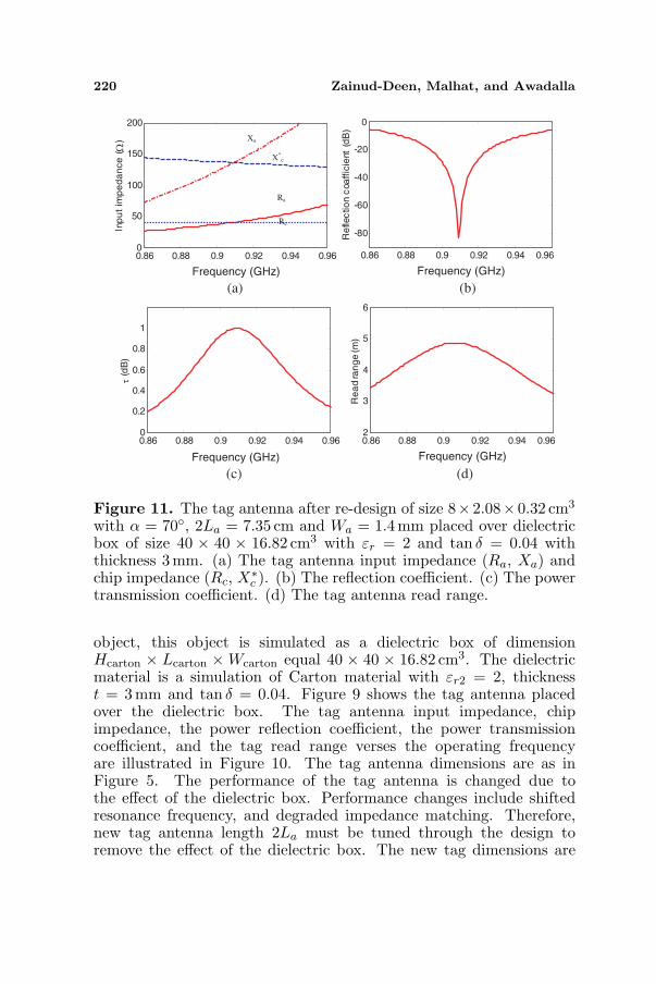
Figure 11. The tag antenna after re-design of size 8×2.08×0.32 cm3
with α = 70, 2La = 7.35 cm and Wa = 1.4mm placed over dielectricbox of size 40 × 40 × 16.82 cm3 with εr = 2 and tan δ = 0.04 withthickness 3 mm. (a) The tag antenna input impedance (Ra, Xa) andchip impedance (Rc, X∗
c ). (b) The reflection coefficient. (c) The powertransmission coefficient. (d) The tag antenna read range.
object, this object is simulated as a dielectric box of dimensionHcarton × Lcarton × Wcarton equal 40 × 40 × 16.82 cm3. The dielectricmaterial is a simulation of Carton material with εr2 = 2, thicknesst = 3 mm and tan δ = 0.04. Figure 9 shows the tag antenna placedover the dielectric box. The tag antenna input impedance, chipimpedance, the power reflection coefficient, the power transmissioncoefficient, and the tag read range verses the operating frequencyare illustrated in Figure 10. The tag antenna dimensions are as inFigure 5. The performance of the tag antenna is changed due tothe effect of the dielectric box. Performance changes include shiftedresonance frequency, and degraded impedance matching. Therefore,new tag antenna length 2La must be tuned through the design toremove the effect of the dielectric box. The new tag dimensions are

Progress In Electromagnetics Research B, Vol. 16, 2009 221
20 40
30
-150
60
-120
90-90
120
-60
150
-30
180
0
20 40
30
210
60
240
90270
120
300
150
330
180
0θ φ
(a) E-plane (b) H-plane
Figure 12. The E-plane and H-plane radiation pattern of the tagantenna over dielectric box of size 8 × 2.08 × 0.32 cm3 with α = 70,2La = 7.35 cm and Wa = 1.4mm placed over dielectric box of size40×40×16.82 cm3 with εr2 = 2 and tan δ = 0.04 with thickness 3mm.
0.86 0.88 0.9 0.92 0.94 0.960
1
2
3
4
5
Ga
in (
dB
)
Frequency (GHz)
Figure 13. The tag antenna gain G verses frequency for tag antenna ofsize 8×2.08×0.32 cm3 with α = 70, 2La = 7.35 cm and Wa = 1.4mmover dielectric box of size 40 × 40 × 16.82 cm3 with εr = 2 andtan δ = 0.04 with thickness 3mm.
8 × 2.08 × 0.32 cm3, with 2La = 7.35 cm and Wa = 1.4 mm. Theperformances of tag antenna on the dielectric box are depicted inFigure 11. The corresponding E-plane and H-plane radiation patternat 910MHz and the tag antenna gain versus the operating frequencyare shown in Figure 12 and Figure 13 respectively.
An object with length Lobject = 29.4 cm, width Wobject = 6.28 cmand height Hobject = 29.4 cm with dielectric permittivity εr3 is placedon the center of the dielectric box and the tag antenna is attached to thedielectric box as shown in Figure 14. The object is made from differentmaterials includes (1) Arlon AD 320 (tm) with εr3 = 3.2 and dielectricloss tan δ = 0.003 (object1), (2) glass with εr3 = 5.5 (object2), and(3) copper with σ = 5.8 × 10⁸ s/m (object3). The performance ofthe tag in the presence of the dielectric box and different object

222 Zainud-Deen, Malhat, and Awadalla
(a) 3-D view
ε
(b) Side view
Wobject
Lobject
Wobject
Hobject
r=1
Hobjecttcarton
ε
Figure 14. The tag antenna configuration over carton box with theobject placed on its center. The object dimensions Lobject ×Wobject ×Hobject = 29.4× 29.4× 6.28 cm3 of different materials.
0.86 0.88 0.9 0.92 0.94 0.96
-80
-60
-40
-20
0
Frequency (GHz)
Re
fle
cti
on
co
aff
icie
nt
(dB
)
0.86 0.88 0.9 0.92 0.94 0.960
0.2
0.4
0.6
0.8
1
Frequency (GHz)
τ (
dB
)
0.86 0.88 0.9 0.92 0.94 0.962
4
6
8
Frequency (GHz)
Re
ad
ra
ng
e(m
)
(c)
(b) (a)
No object
Object (1)
Object (2)
Object (3)
Figure 15. The tag antenna attached to carton box contains differentobjects. (a) The reflection coefficient, (b) The power transmissioncoefficient, (c) The tag antenna read range.

Progress In Electromagnetics Research B, Vol. 16, 2009 223
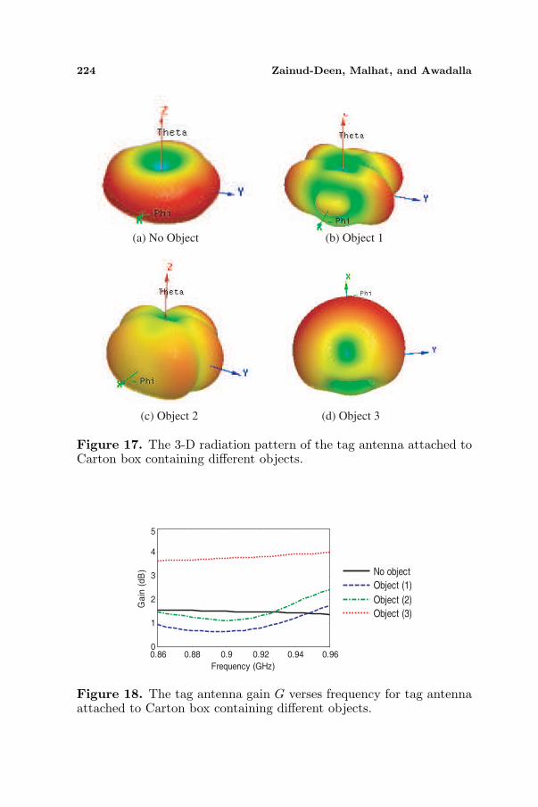
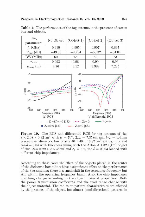
materials is depicted in Figure 15 with their performance listed inTable 1. The radiation characteristics of the tag antenna with differentobjects are displayed in Figure 16. Figure 15 shows that the matchingcondition is still preserved within the entire band considered. The 3Dradiation pattern at 910MHz for different objects is shown in Figure 17.Figure 18 shows the tag gain versus the frequency for each object.
E-plane H-plane
(a) Object (1)
50 100
30
-150
60
-120
90-90
120
-60
150
-30
180
0
50 100
30
-150
60
-120
90-90
120
-60
150
-30
180
0
50 100
30
210
60
240
90270
120
300
150
330
180
0
50 100
30
-150
60
-120
90-90
120
-60
150
-30
180
0
50 100
30
-150
60
-120
90-90
120
-60
150
-30
180
0
50100
30
210
60
240
90270
120
300
150
330
180
0
Eθ
Eφ
E-plane H-plane
(b) Object (2)
E-plane H-plane
(c) Object (3)
Eθ
Eφ
50 100
30
-150
60
-120
90-90
120
-60
150
-30
180
0
50100
30
210
60
240
90270
120
300
150
330
180
0
Eθ
Eφ
50100
30
-150
60
-120
90-90
120
-60
150
-30
180
0
E
Figure 16. The E-plane and H-plane radiation pattern of the tagantenna attached to Carton box containing different objects.
224 Zainud-Deen, Malhat, and Awadalla
(a) No Object (b) Object 1
(c) Object 2 (d) Object 3
Figure 17. The 3-D radiation pattern of the tag antenna attached toCarton box containing different objects.
0.86 0.88 0.9 0.92 0.94 0.960
1
2
3
4
5
Frequency (GHz)
Ga
in (
dB
) No object
Object (1)
Object (2)
Object (3)
Figure 18. The tag antenna gain G verses frequency for tag antennaattached to Carton box containing different objects.
Progress In Electromagnetics Research B, Vol. 16, 2009 225
Table 1. The performance of the tag antenna in the presence of cartonbox and objects.
Tagparameters
No Object (Object 1) (Object 2) (Object 3)
fo (GHz) 0.910 0.905 0.907 0.897Γmin (dB) −49.86 −40.34 −53.32 −34.04BW(MHz) 60 55 62 53
τmax 0.993 0.98 0.99 0.96Rmax (m) 4.76 3.12 3.988 7.225
(a) RCS (b) differential RCS
860 880 900 920 940 960-25
-20
-15
-10
-5
Frequency (GHz)
σ (
dB
)
860 880 900 920 940 960-35
-30
-25
-20
-15
-10
Frequency (GHz)
∆σ
(dB
)
ZL=Z c*= 40-j133 , ZL= 0, ZL=
ZL=540-j133, ZL=40-j633
∞
Figure 19. The RCS and differential RCS for tag antenna of size8 × 2.08 × 0.32 cm3 with α = 70, 2La = 7.35 cm and Wa = 1.4mmplaced over dielectric box of size 40× 40× 16.82 cm3 with εr = 2 andtan δ = 0.04 with thickness 3 mm, with the Arlon AD 320 (tm) objectof size 29.4 × 29.4 × 6.28 cm and εr = 3.2, tan δ = 0.003 loaded withdifferent chip impedances.
According to these cases the effect of the objects placed in the centerof the dielectric box didn’t have a significant effect on the performanceof the tag antenna; there is a small shift in the resonance frequency butstill within the operating frequency band. Also, the chip impedancematching change according to the object material properties. Boththe power transmission coefficients and the read range change withthe object material. The radiation pattern characteristics are affectedby the presence of the object, but almost omni-directional patterns in

226 Zainud-Deen, Malhat, and Awadalla
the H-plane are observed. Figure 18 shows the RCS and differentialRCS for conjugated–matched antenna, loaded with ZL = 40− j133Ω,ZL = 0Ω, ZL = ∞Ω, ZL = 540− j133Ω and ZL = 40− j633Ω.
4. CONCLUSION
A fractal dipole antenna for passive UHF RFID applications hasbeen proposed, analyzed and designed. The tag antenna consistsof a modified Koch fractal dipole antenna sandwiched between twodielectric layers. The tag antenna has been designed and optimizedusing the finite element method. The proposed tag antenna can operateat 910MHz. The antenna is simple and has good impedance matchingwith the chip impedance. The variation of the magnitude of theopen- circuit voltage and the polarization mismatch factor against theoperating frequency are explained. The input impedance, reflectioncoefficient, the power transmission coefficient and the read range areinvestigated. The RCS and differential RCS are calculated for differentload impedances. There is a small shift in the resonance frequency dueto the different objects placed inside the dielectric box around 13MHz.
ACKNOWLEDGMENT
The authors would like to thank Prof. Dr Ahmed Kishk for valuablediscussions, The authors are also grateful to the technical reviewers ofthe paper for their helpful comments.
REFERENCES
1. Chen, Z. N., Antennas for Portable Devices, Chapter 3, JohnWiely & Sons, Ltd., UK, 2007.
2. Chen, S.-Y. and P. Hsu, “CPW-fed folded-slot antenna for 5.8 GHzRFID tags,” Electronic Lett., Vol. 24, 1516–1517, Nov. 2004.
3. Padhi, S. K., N. C. Karmakar, C. L. Law, and S. Aditya, “Adual polarized aperture coupling circular patch antenna using aC-shaped coupling slot,” IEEE Trans. Antennas Propag., Vol. 51,No. 12, 3295–3298, Dec. 2003.
4. Marrocco, G., “Gain-optimized self-resonant meander lineantennas for RFID applications,” Antennas Wireless Propag.Lett., Vol. 2, No. 21, 302–305, 2003.
5. Hirvonen, M., P. Pursula, K. Jaakkola, and K. Laukkanen,“Planar inverted-F antenna for radio frequency identification,”Electronic Lett., Vol. 40, 848–850, Jul. 2004.

Progress In Electromagnetics Research B, Vol. 16, 2009 227
6. Qing, X.-M. and N. Yang, “A folded dipole antenna for RFID,”Proc. IEEE Antennas and Propagation Soc. Int. Symp., Vol. 1,97–100, Jun. 2004.
7. Foster, P. R. and R. A. Burberry, “Antenna problems in RFIDsystems,” Proc. Inst. Elect. Eng. Colloquium RFID Technology,3/1–3/5, Oct. 1999.
8. Tan, K. G., A. R. Wasif, and C.-P. Tan, “Objects trackingutilizing square grid RFID reader antenna network,” Journal ofElectromagnetic Waves and Applications, Vol. 22, No. 1, 27–38,2008.
9. Shi, X., F. Wei, Q. Huang, L. Wang, and X.-W. Shi, “Novel binarysearch algorithm of backtracking for RFID tag anti-collision,”Progress In Electromagnetics Research B, Vol. 9, 97–104, 2008.
10. Li, X., L. Yang, S.-X. Gong, Y.-J. Yang, and J.-F. Liu, “Acompact folded printed dipole antenna for UHF RFID reader,”Progress In Electromagnetics Research Letters, Vol. 6, 47–54, 2009.
11. Best, S. R., “On the performance properties of the Koch fractaland other bent wire monopoles,” IEEE Trans. Antennas Propag.,Vol. 51, No. 6, 1292–1300, Jun. 2003.
12. Seshagiri Rao, K. V., P. V. Nikitin, and S. F. Lam, “Antennadesign for UHF RFID tags: A review and a practical application,”IEEE Trans. Antennas Propag., Vol. 51, No. 12, 3870–3876,Dec. 2005.
13. Nikitin, P. V. and K. V. S. Rao, “Theory and measurement ofbackscattering from RFID tags,” IEEE Antennas Propag. Mag.,Vol. 48, 212–218, Dec. 2006.
14. Loo, C.-H., K. Elmahgoub, F. Yang, A. Elsherbeni, D. Kajfez,A. Kishk, and T. Elsherbeni, “Chip impedance matching forUHF RFID tag antenna design,” Progress In ElectromagneticsResearch, PIER 81, 359–370, 2008.
15. Baliarda, C. P., J. Romeu, and A. Cardama, “The Kochmonopole: A small fractal antenna,” IEEE Trans. AntennasPropag., Vol. 48, No. 11, 1773–1781, Nov. 2000.
16. Da Costa, K. Q. and V. Dmitriev, “Theoretical analysis of amodified Koch monopole with reduced dimensions,” IEE Proc.- Microw. Antennas Propag., Vol. 153, No. 5, 475–479, Oct. 2006.
17. Wunsch, A. D., “The vector effective length of slot antennas,”IEEE Trans. Antennas Propag., Vol. 39, No. 5, 705–709, May1991.
18. Zainud-Deen, S. H., “Polarization losses in normal modehelical antenna,” 1995 IEEE/AP-S International Symposium and

228 Zainud-Deen, Malhat, and Awadalla
USNC/URSI Radio Science Meeting, California, 1883–1886, 1995.19. Fuschini, F., C. Piersanti, F. Paolazzi, and G. Falciasecca,
“Analytical approach to the backscattering from UHF RFIDtransponder,” Antennas Wireless Propag. Lett., Vol. 53, No. 12,33–35, 2008.
20. Pursula, P., D. Sandstrom, and K. Jaakkola, “Backscattering-based measurement of reactive antenna input impedance,” IEEETrans. Antennas Propag., Vol. 56, No. 2, 469–474, Feb. 2008.
21. Penttila, K., M. Keskilammi, L. Sydanheimo, and M. Kivikoski,“Radar cross-section analysis for passive RFID systems,” IEEProc. - Microw. Antennas Propag., Vol. 153, No. 1, Feb. 2006.
22. Youla, D. C., “On scattering matercies normalized to complexport numbers,” Proc. I. R. E., Vol. 49, 12–21, Jul. 1961.
23. Dong, X. and T. An, “A new FEM approach for open boundaryLaplace’s problem,” IEEE Trans. Microw. Theory Tech., Vol. 44,157–160, Jan. 1996.
24. Zhou, X. and G. W. Pan, “Application of physical spline finiteelement method (PSFEM) to full wave analysis of waveguide,”Progress In Electromagnetics Research, PIER 60, 19–41, 2006.
25. Gavrilovic, M. M. and J. P. Webb, “Accuracy control in theoptimization of microwave devices by finite element methods,”IEEE Trans. Microw. Theory Tech., Vol. 50, No. 8, 1901–1911,Aug. 2002.
26. Polycarpou, A. C., Introduction to Finite Element Method inElectromagnetics, Morgan & Claypool Publishers’ series, USA,2006.
27. Garg, R., P. Bhartia, I. Bahland, and A. Ittipiboon, MicrostripAntenna Design Handbook, Artech House, Inc., Norwood, USA,2001.
28. Johonson, J. and R Sainati, “Investigation of UHF RFID tagbackscatter,” Proc. IEEE Antennas and Propagation Soc. Int.Symp., Vol. 1, 2753–2755, Jun. 2007.
![Multiband Monopole Antenna with Sector-Nested Fractalfractal antennas in recent years include Sierpinski fractal antenna[8], Koch fractal antenna [9] and Minkowski antenna [10] . In](https://img.pdfslide.us/doc/110x75/5e76c468024e970eb01c097c/multiband-monopole-antenna-with-sector-nested-fractal-fractal-antennas-in-recent.jpg)