Embed Size (px)
Citation preview

FPGA tutorial
Lecture 2Monday 07.09.2015 – 16:00
Jochen Steinmann
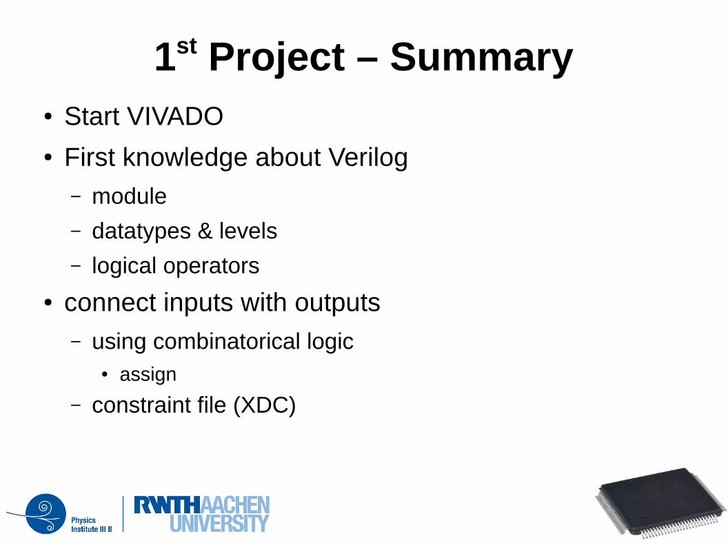
1st Project – Summary● Start VIVADO● First knowledge about Verilog
– module
– datatypes & levels
– logical operators
● connect inputs with outputs– using combinatorical logic
● assign
– constraint file (XDC)
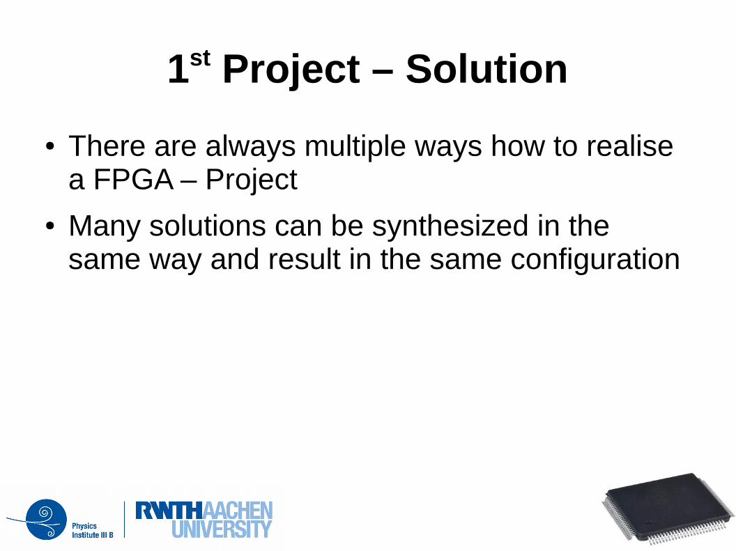
1st Project – Solution
● There are always multiple ways how to realise a FPGA – Project
● Many solutions can be synthesized in the same way and result in the same configuration
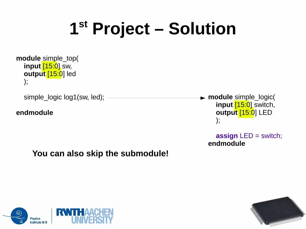
1st Project – Solution
module simple_top( input [15:0] sw, output [15:0] led ); simple_logic log1(sw, led); endmodule
module simple_logic( input [15:0] switch, output [15:0] LED ); assign LED = switch;endmodule
You can also skip the submodule!
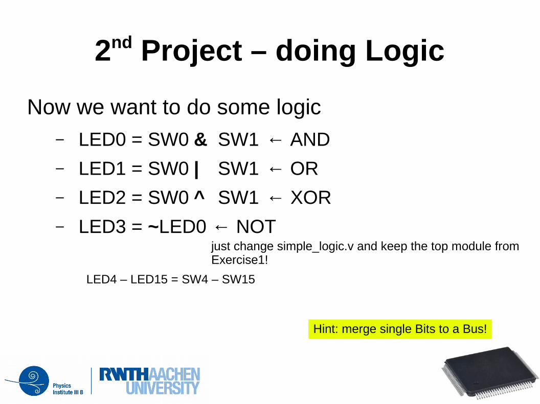
2nd Project – doing Logic
Now we want to do some logic– LED0 = SW0 & SW1 ← AND
– LED1 = SW0 | SW1 ← OR
– LED2 = SW0 ^ SW1 ← XOR
– LED3 = ~LED0 ← NOTjust change simple_logic.v and keep the top module from Exercise1!
LED4 – LED15 = SW4 – SW15
Hint: merge single Bits to a Bus!

2nd Project – Solutionmodule simple_logic( input [7:0] switch, output [7:0] LED ); assign LED[0] = switch[0] & switch[1]; assign LED[1] = switch[0] | switch[1]; assign LED[2] = switch[0] ^ switch[1]; assign LED[3] = ~ LED[0]; assign LED[15:4] = switch[15:4];endmodule
assign LED = {switch[15:4] , ~(switch[0] & switch[1]), switch[0] ^ switch[1], switch[0] | switch[1]};
Alternative: → Same Function
without joining all together to a bus again.

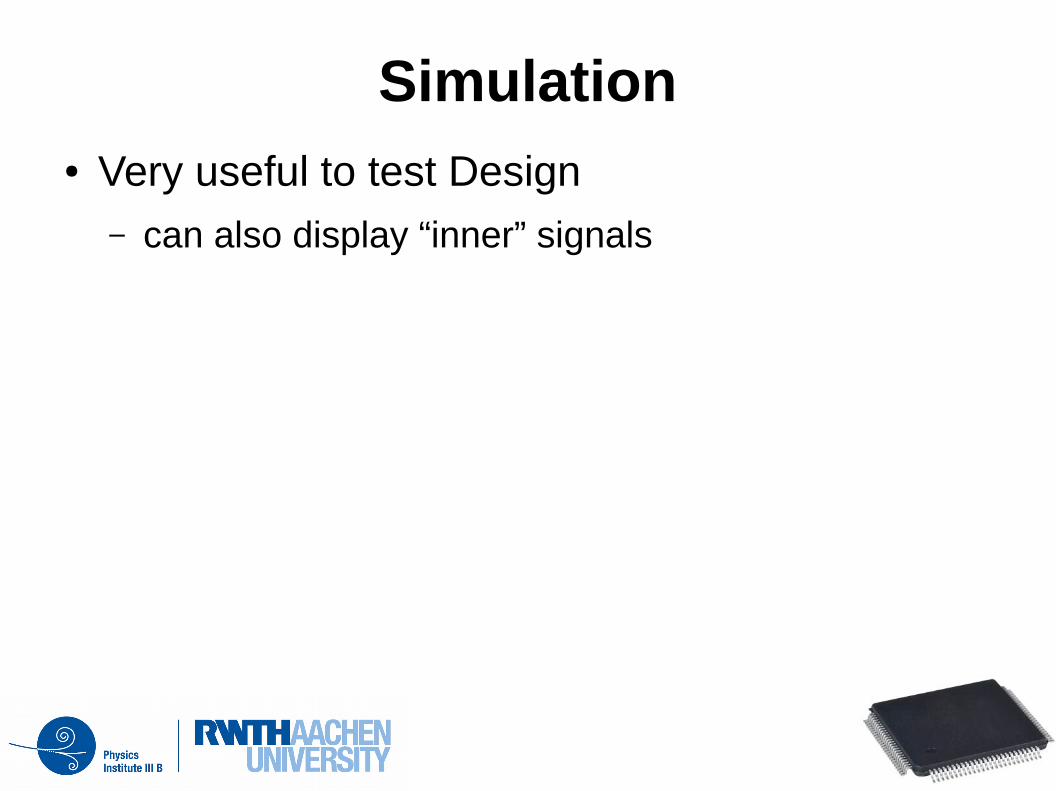
Simulation● Very useful to test Design
– can also display “inner” signals

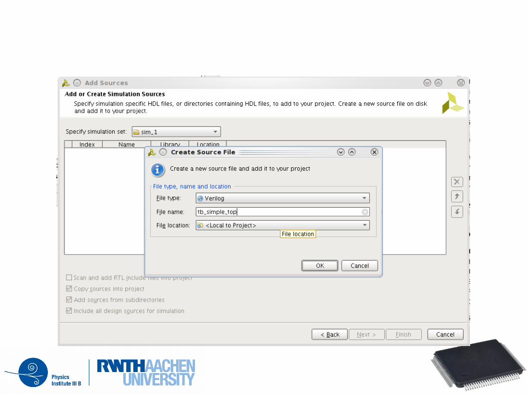
Add new Source
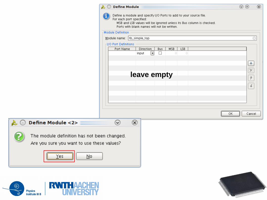
leave empty
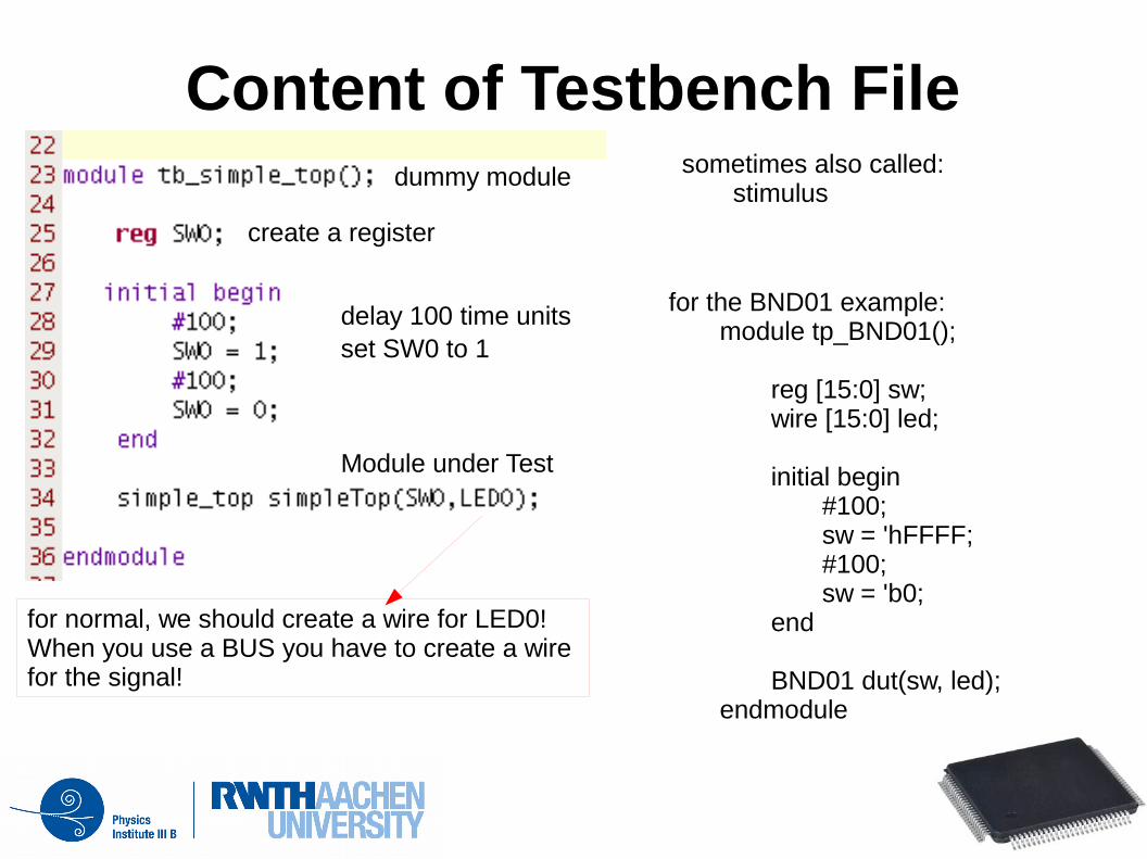
Content of Testbench File
delay 100 time unitsset SW0 to 1
dummy module
create a register
Module under Test
for normal, we should create a wire for LED0!When you use a BUS you have to create a wire for the signal!
sometimes also called:stimulus
for the BND01 example:module tp_BND01();
reg [15:0] sw;wire [15:0] led;
initial begin#100;sw = 'hFFFF;#100;sw = 'b0;
end
BND01 dut(sw, led);endmodule
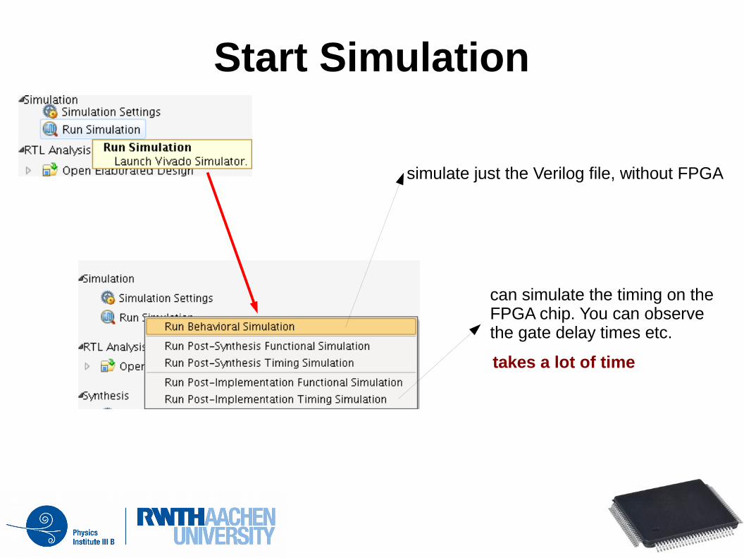
Start Simulation
simulate just the Verilog file, without FPGA
can simulate the timing on the FPGA chip. You can observethe gate delay times etc.
takes a lot of time
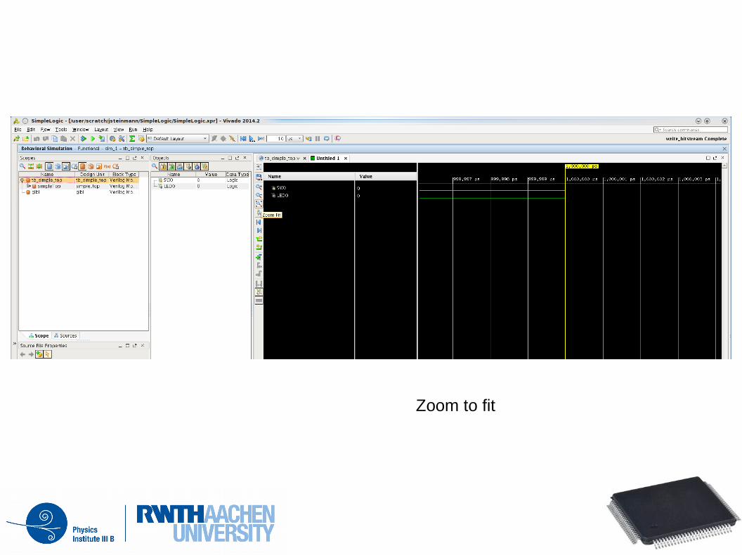
Zoom to fit
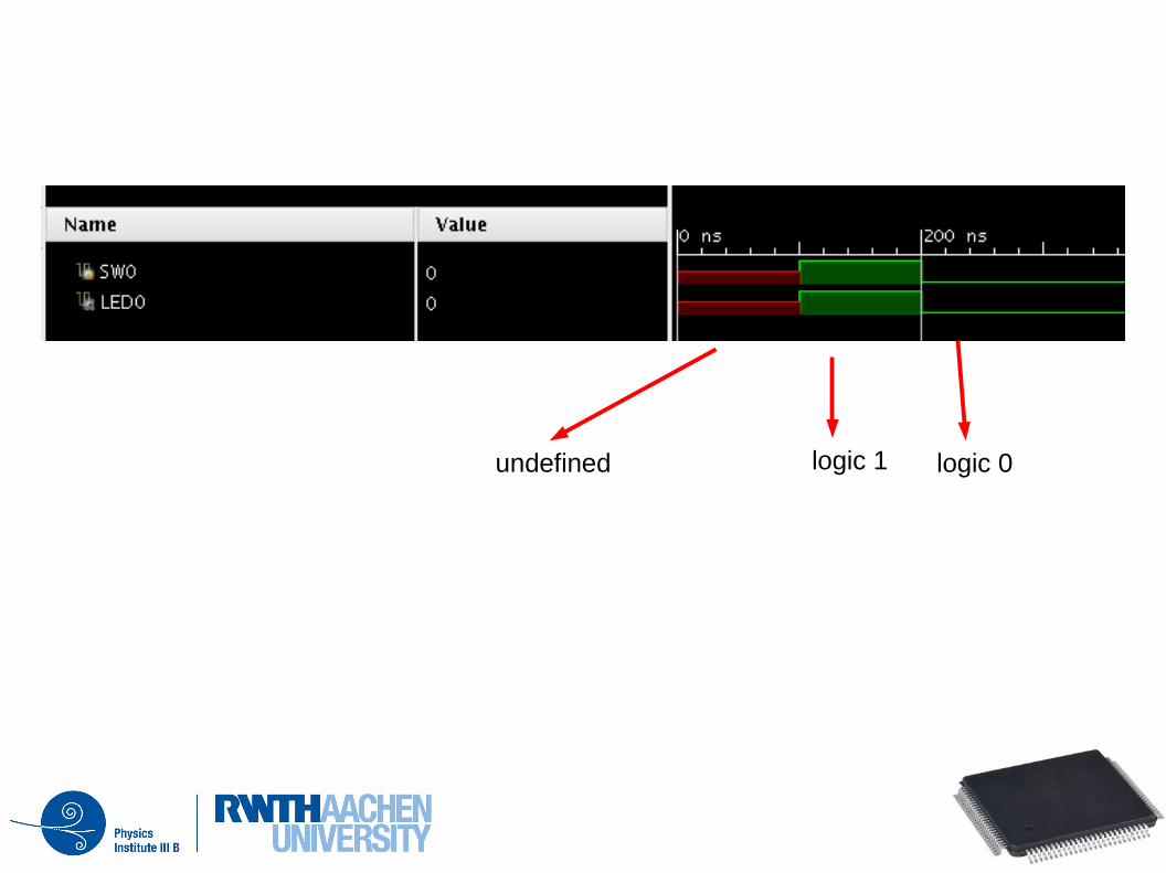
undefined logic 1 logic 0

Clock
Clock – Why?
● Until now only “Glue Logic”– simple logic only
– output action is related to input
– This “mode” is used for trigger generation:→ trg = (A & B) || (A & C)
– But if we want to introduce timing, e.g. dead-time after a trigger
● we need to react on something but not the input→ CLOCK
Use of Clock
● We want to let the FPGA doing thing for us– Memory storage RAM need a clock to refresh
– Digital communication to other electronics or PC
● Delays– compensate cable length
– artificial dead times → Trigger Veto
● Measurements of the time between two events:– Drift velocity measurement in a TPC
– Time of Flight measurements to distinguish particles
Clock Requirements
● Requirements:– stable frequency
– stable phase to other clocks
– stable signal
– reproducible● low temperature dependency● low dependency on environment
Need external reference Clock generatorMost FPGAs do not have an internal clock generator!
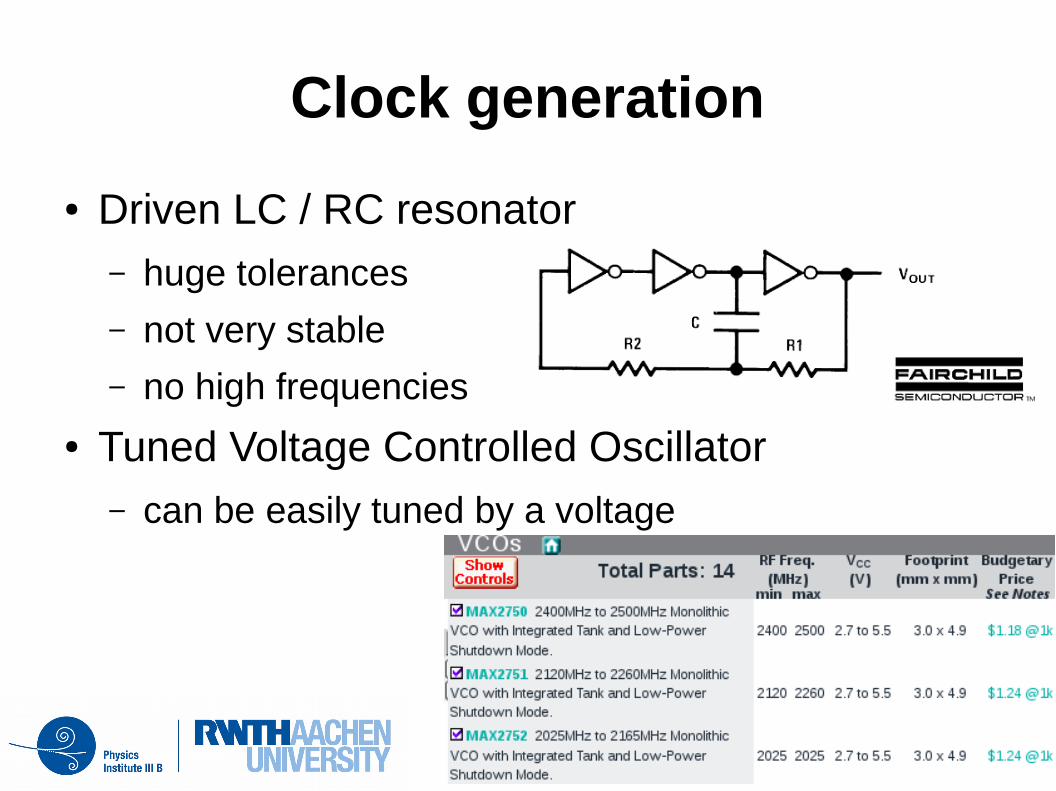
Clock generation
● Driven LC / RC resonator– huge tolerances
– not very stable
– no high frequencies
● Tuned Voltage Controlled Oscillator– can be easily tuned by a voltage
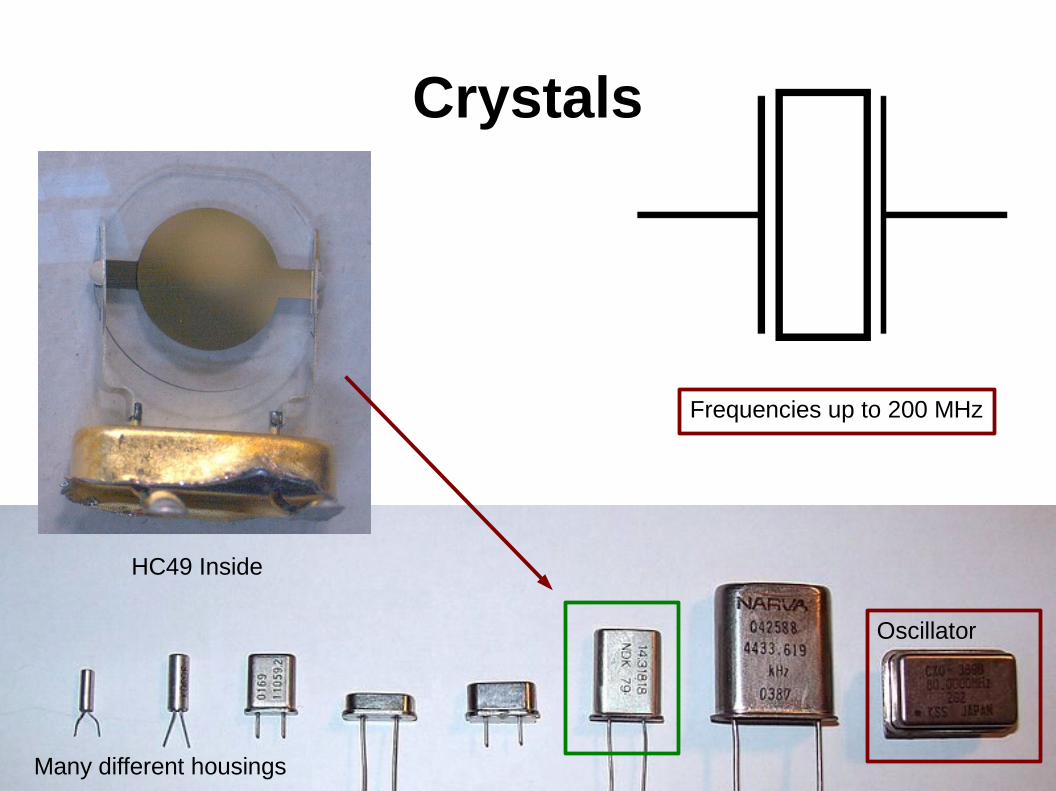
Crystals
Frequencies up to 200 MHz
HC49 Inside
Many different housings
Oscillator
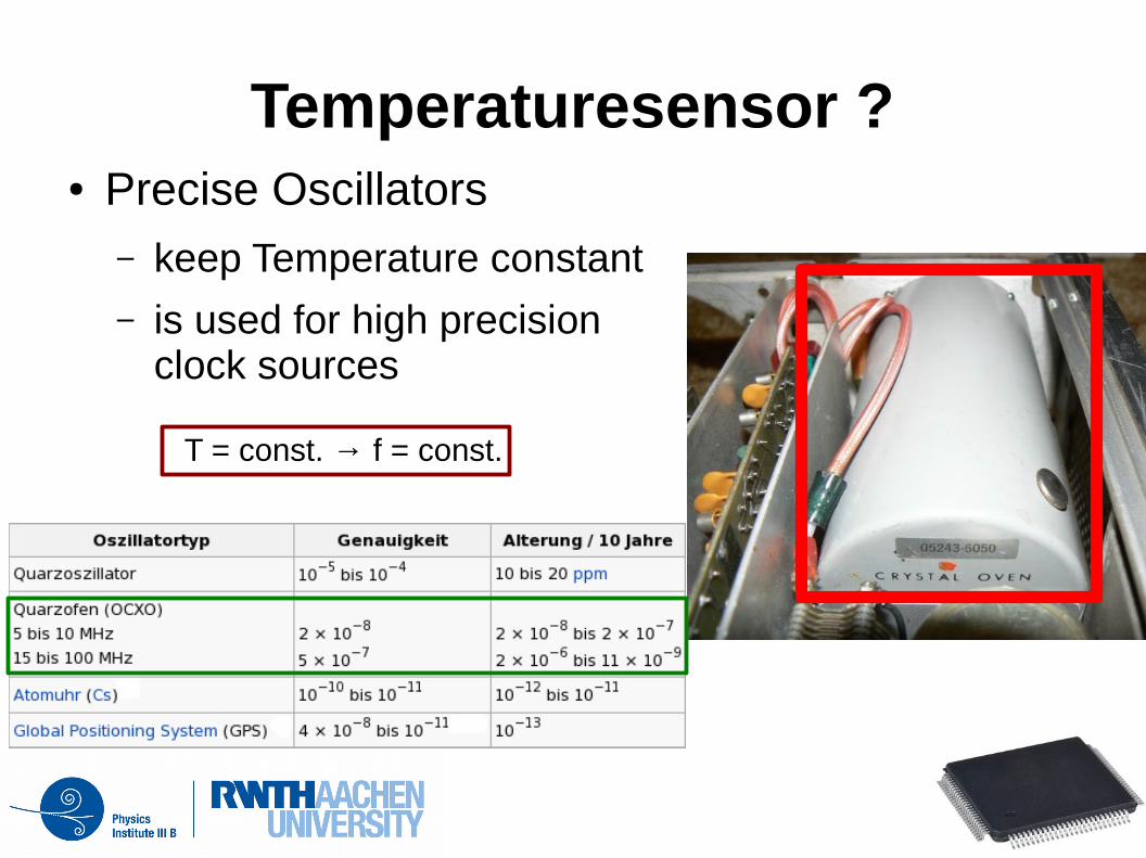
Temperaturesensor ?● Precise Oscillators
– keep Temperature constant
– is used for high precisionclock sources
T = const. → f = const.
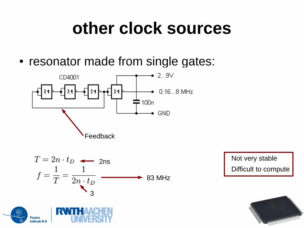
other clock sources
● resonator made from single gates:
Feedback
2ns
3
83 MHz
Not very stable
Difficult to compute
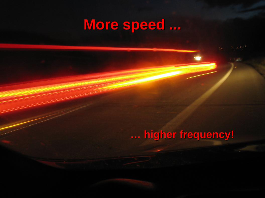
More speed ...More speed ...
… … higher frequency!higher frequency!

Stable high speed clock...
● Crystals and Oscillators are only available up to ~ 200MHz!
● What if we need ~ 1GHz ?
All you need is a Voltage Controlled Oscillatorand a slower reference clock!
Frequency Multiplication!
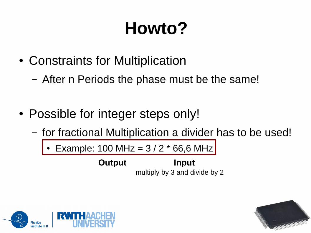
Howto?
● Constraints for Multiplication– After n Periods the phase must be the same!
● Possible for integer steps only!– for fractional Multiplication a divider has to be used!
● Example: 100 MHz = 3 / 2 * 66,6 MHz
Output Inputmultiply by 3 and divide by 2
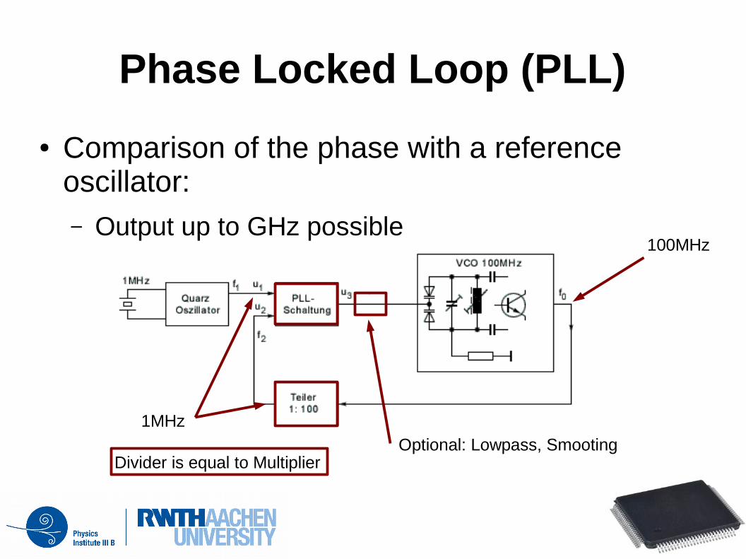
Phase Locked Loop (PLL)
● Comparison of the phase with a reference oscillator:– Output up to GHz possible
1MHz
100MHz
Optional: Lowpass, SmootingDivider is equal to Multiplier
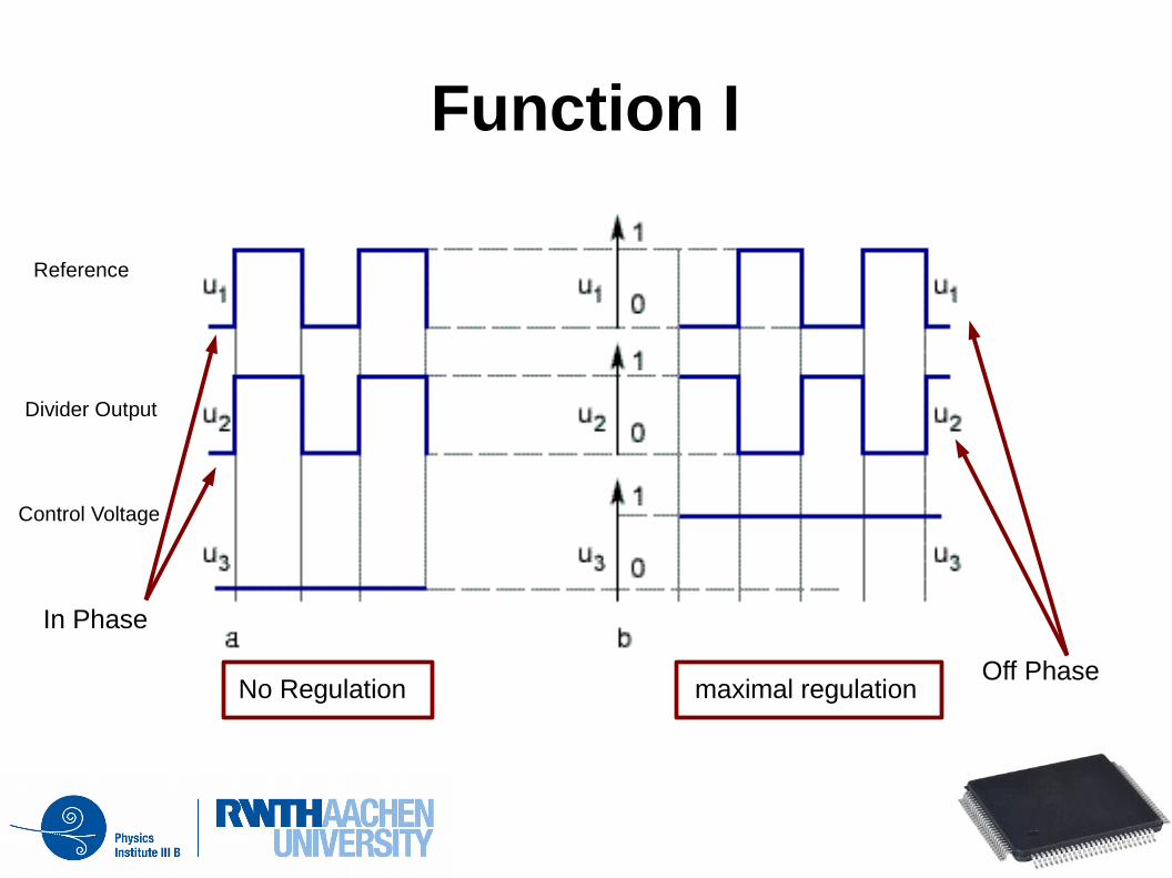
Function I
Reference
Divider Output
Control Voltage
In Phase
No RegulationOff Phase
maximal regulation
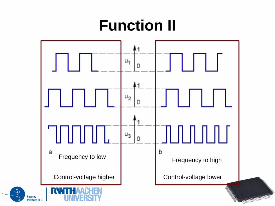
Function II
Frequency to low Frequency to high
Control-voltage higher Control-voltage lower
Function III & FPGA
● PLL is stable operating, when the output voltage is stable. (u3 = 0)
● There are so called Lock-In detectors available, which are able to detect this case.
● FPGAs have build in PLL blocks, which can be used to create a stable clock.– mainly used to derived secondary (slower) clocks
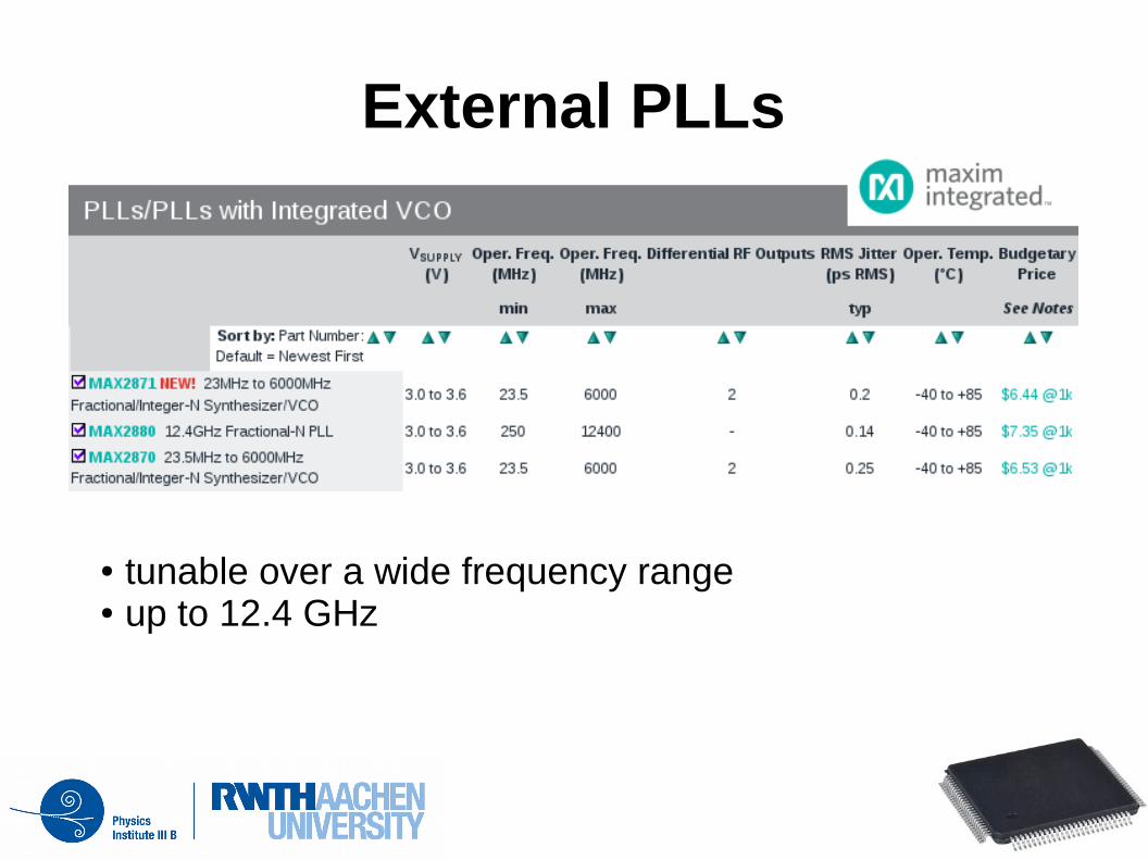
External PLLs
● tunable over a wide frequency range● up to 12.4 GHz
Clock in Experiments
● Stability is observed by a slower “reference Clock” and a counter– Possible reference clock sources
● GPS → many GPS modules supply a 1 PPS pulse● Atomic Clocks → DCF77● Rubidium Clock Generators which can also supply any
Master Clock signal
GPS as Reference
● Often used in experiments– OPERA
– T2K
● Precise clock output by – Rubidium Reference Clock → 10MHz
● Huge accuracy and precision
Helpful, when timestamps should be matched over large distances.
Clock inside FPGA
● Routing of clock inside the FPGA is a challenge for VIVADO
● Requirements:– small clock delay
● at every point inside the FPGA
– phase must match signal● most modules latch their data on rising or falling edge
● There is a special high speed net inside the FPGA, which is only used for clock distribution
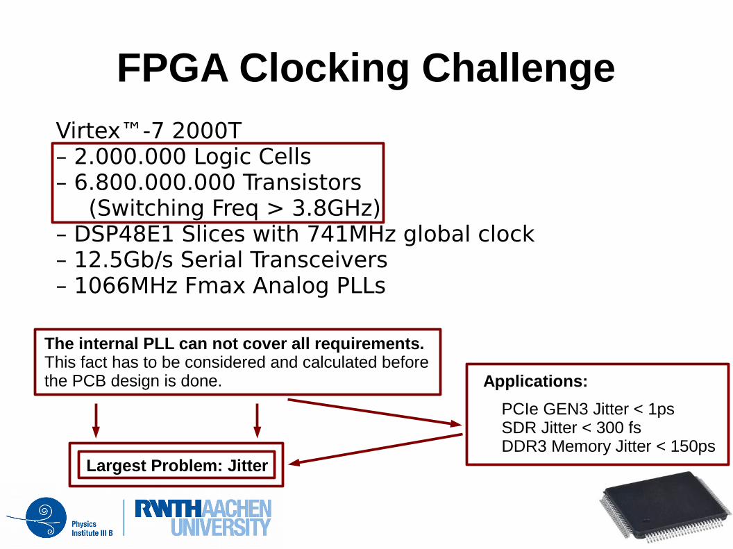
FPGA Clocking Challenge
Virtex™-7 2000T– 2.000.000 Logic Cells– 6.800.000.000 Transistors
(Switching Freq > 3.8GHz)– DSP48E1 Slices with 741MHz global clock– 12.5Gb/s Serial Transceivers– 1066MHz Fmax Analog PLLs
PCIe GEN3 Jitter < 1psSDR Jitter < 300 fsDDR3 Memory Jitter < 150ps
Applications:
The internal PLL can not cover all requirements. This fact has to be considered and calculated before the PCB design is done.
Largest Problem: Jitter
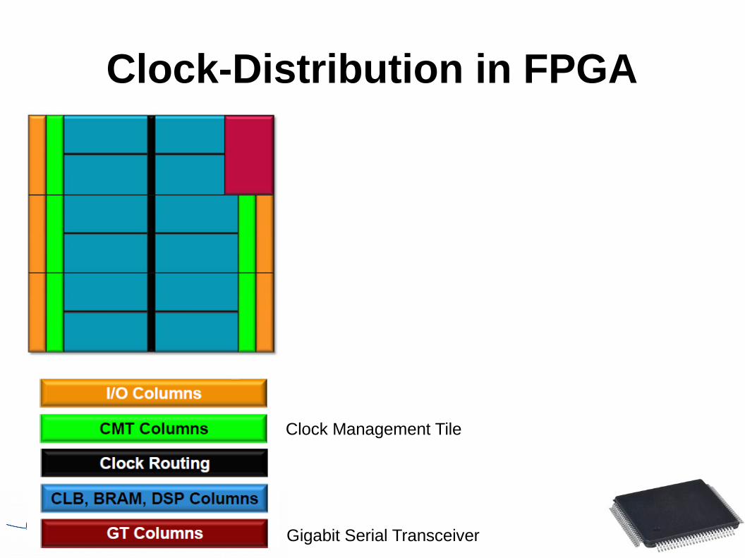
Clock-Distribution in FPGA
Clock Management Tile
Gigabit Serial Transceiver
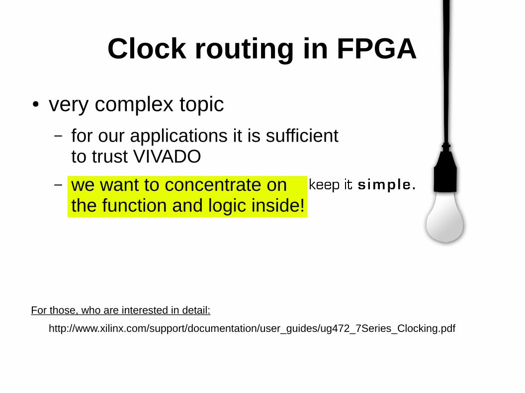
Clock routing in FPGA
● very complex topic– for our applications it is sufficient
to trust VIVADO
– we want to concentrate onthe function and logic inside!
For those, who are interested in detail:
http://www.xilinx.com/support/documentation/user_guides/ug472_7Series_Clocking.pdf
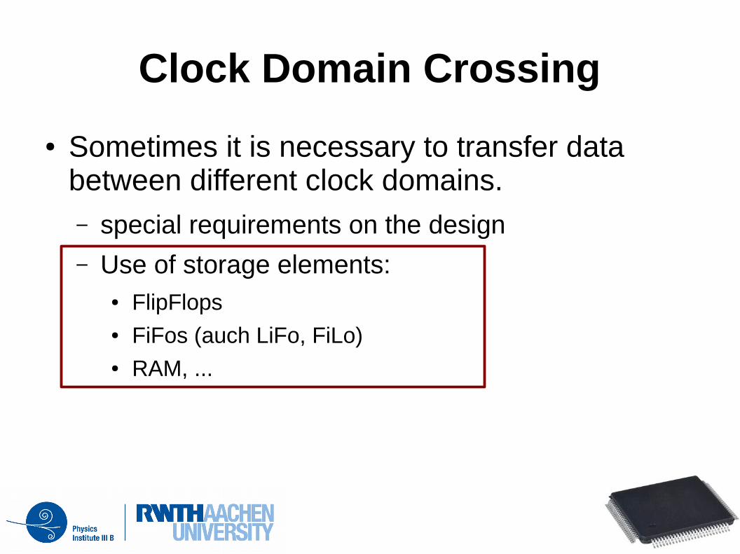
Clock Domain Crossing
● Sometimes it is necessary to transfer data between different clock domains.– special requirements on the design
– Use of storage elements:● FlipFlops● FiFos (auch LiFo, FiLo)● RAM, ...
Gated Clock
● If the clock is switched of for non used areas / modules, power can be saved.
● Clock switching must be done via special clock gates.
● Never use a single AND-gate to switch off the clock.
● If you need to use a gated clock, always have a look at the RTL and check for right implementation.
Why is clock gating problematic?
● When a simple clock gate is switched on– it is not done synchronous to the main clock
– Very short pulses might appear → Glitch
● Runtime delays inside the gate– a phase difference between input and output
Some more …
● If high speed frequencies are used, one has to think a bit about the design and how it should be realised.
● Data should be transferred on a defined edge of the clock (posedge or negedge)
42
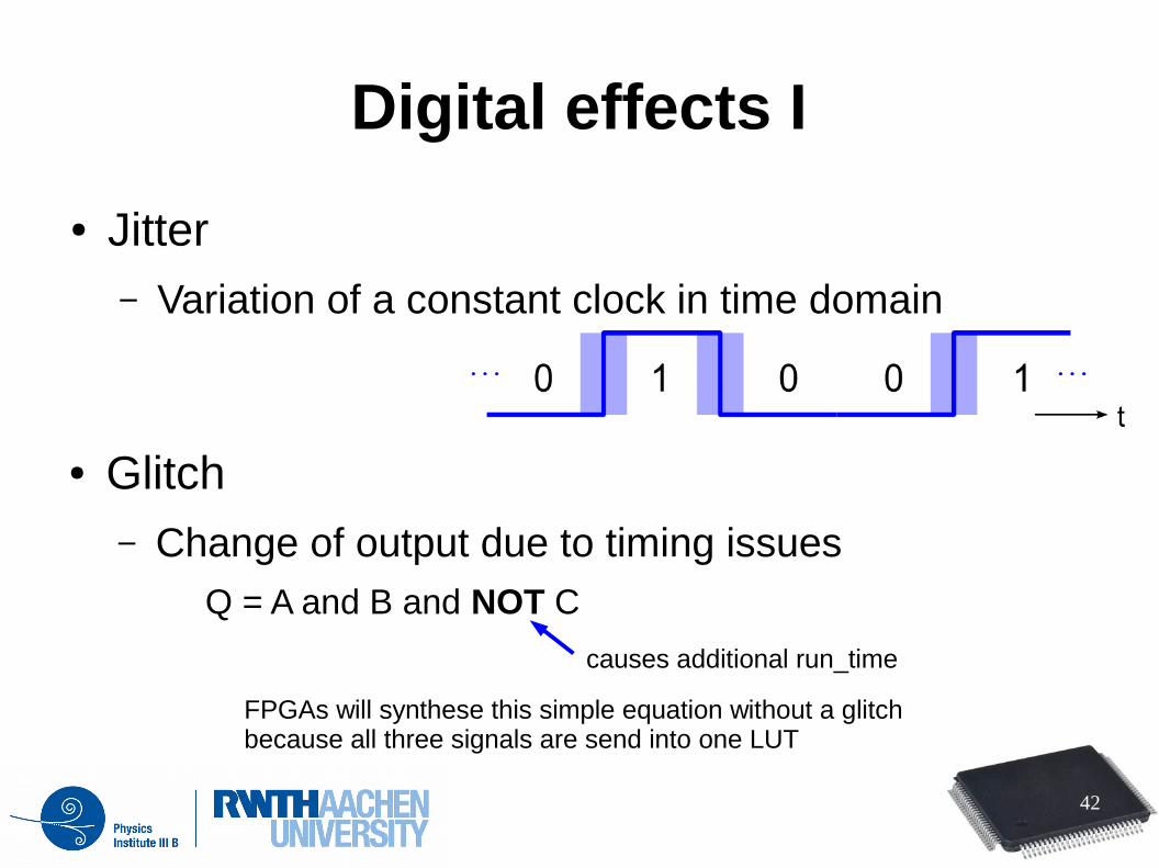
Digital effects I
● Jitter– Variation of a constant clock in time domain
● Glitch– Change of output due to timing issues
Q = A and B and NOT C
causes additional run_time
FPGAs will synthese this simple equation without a glitchbecause all three signals are send into one LUT

Verilog Parameter
● Many Code Snippets can be re-used for other applications
● But often the needs are slightly different– need to use 10 instead of 8 Bit
– uses another clock frequency
– wants a different output value
Verilog code can be parameterized!
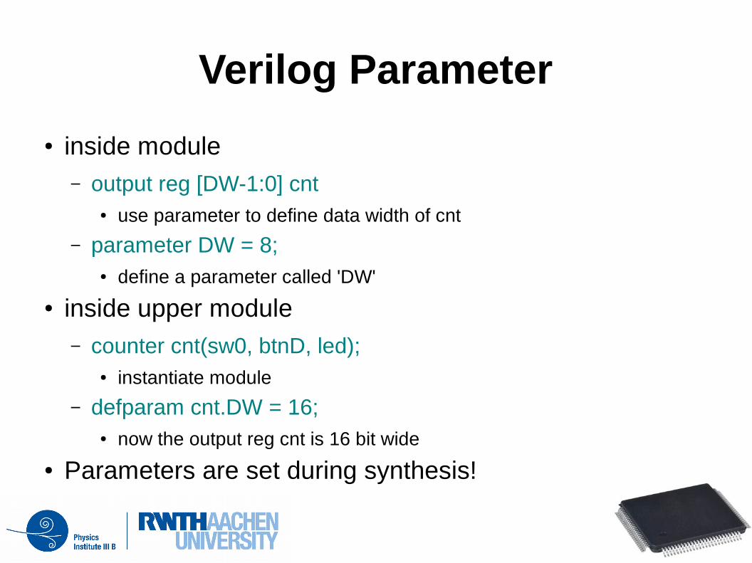
Verilog Parameter
● inside module– output reg [DW-1:0] cnt
● use parameter to define data width of cnt
– parameter DW = 8;● define a parameter called 'DW'
● inside upper module– counter cnt(sw0, btnD, led);
● instantiate module
– defparam cnt.DW = 16;● now the output reg cnt is 16 bit wide
● Parameters are set during synthesis!
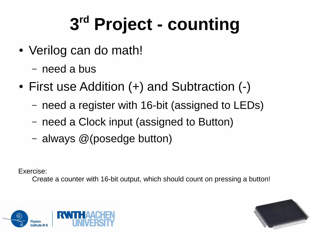
3rd Project - counting● Verilog can do math!
– need a bus
● First use Addition (+) and Subtraction (-)– need a register with 16-bit (assigned to LEDs)
– need a Clock input (assigned to Button)
– always @(posedge button)
Exercise:Create a counter with 16-bit output, which should count on pressing a button!

3rd Project● Counter
– CLK Clock input
– DIR Up / Down
– EN enable
– RST Reset (synchronous)will be executed on next clock event
– VAL 16bit wide register for counting value
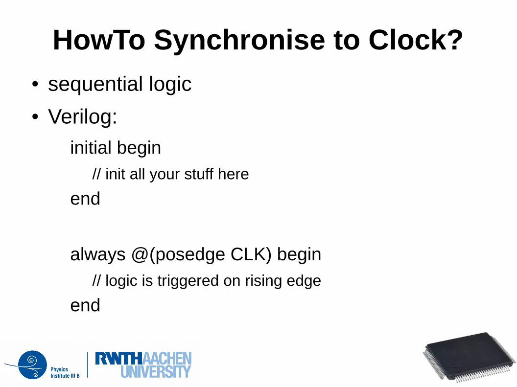
HowTo Synchronise to Clock?● sequential logic● Verilog:
initial begin
// init all your stuff here
end
always @(posedge CLK) begin
// logic is triggered on rising edge
end
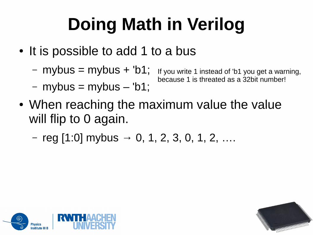
Doing Math in Verilog● It is possible to add 1 to a bus
– mybus = mybus + 'b1;
– mybus = mybus – 'b1;
● When reaching the maximum value the value will flip to 0 again.– reg [1:0] mybus → 0, 1, 2, 3, 0, 1, 2, ….
If you write 1 instead of 'b1 you get a warning,because 1 is threated as a 32bit number!
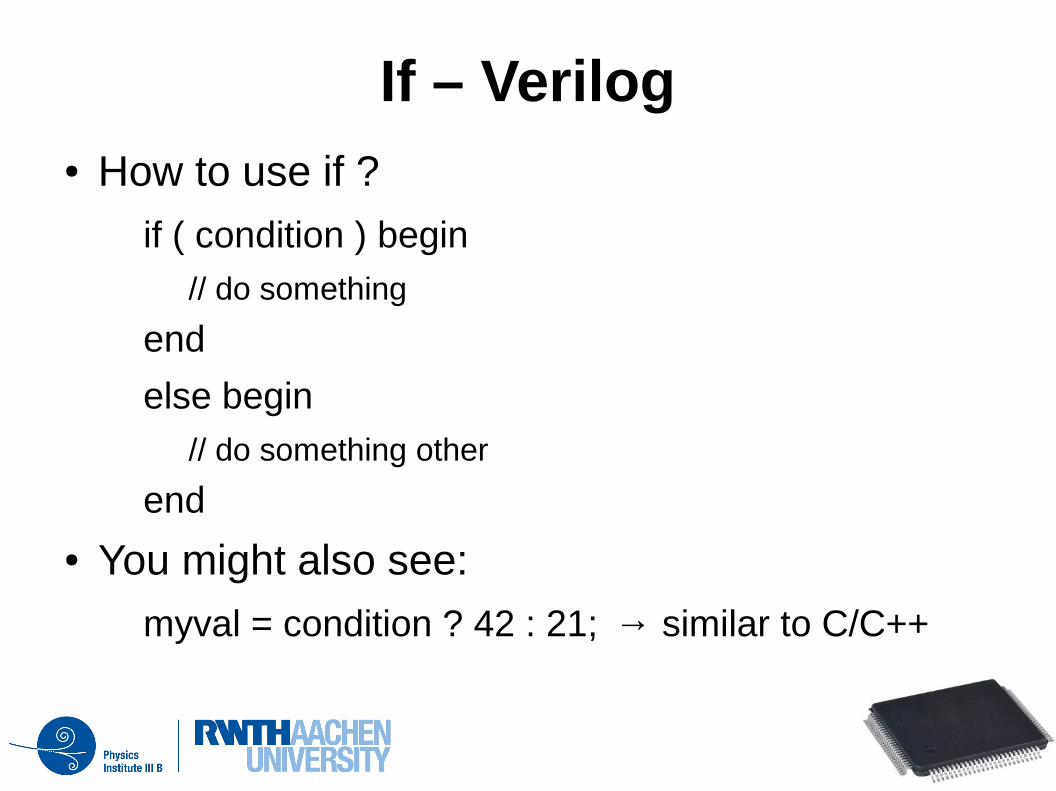
If – Verilog● How to use if ?
if ( condition ) begin
// do something
end
else begin
// do something other
end
● You might also see:
myval = condition ? 42 : 21; → similar to C/C++

Hands-On