Embed Size (px)
Citation preview
FPGA Schematic and HDLDesign Tutorial
Lattice Semiconductor Corporation5555 NE Moore CourtHillsboro, OR 97124(503) 268-8000
November 2008
FPGA Schematic and HDL Design Tutorial ii
CopyrightCopyright © 2008 Lattice Semiconductor Corporation.
This document may not, in whole or part, be copied, photocopied, reproduced, translated, or reduced to any electronic medium or machine-readable form without prior written consent from Lattice Semiconductor Corporation.
TrademarksLattice Semiconductor Corporation, L Lattice Semiconductor Corporation (logo), L (stylized), L (design), Lattice (design), LSC, E2CMOS, Extreme Performance, flexiMAC, flexiPCS, FreedomChip, GAL, GDX, Generic Array Logic, HDL Explorer, IPexpress, ISP, ispATE, ispClock, ispDOWNLOAD, ispGAL, ispGDS, ispGDX, ispGDXV, ispGDX2, ispGENERATOR, ispJTAG, ispLEVER, ispLeverCORE, ispLSI, ispMACH, ispPAC, ispTRACY, ispTURBO, ispVIRTUAL MACHINE, ispVM, ispXP, ispXPGA, ispXPLD, LatticeEC, LatticeECP, LatticeECP-DSP, LatticeECP2, LatticeECP2M, LatticeMico8, LatticeMico32, LatticeSC, LatticeSCM, LatticeXP, MACH, MachXO, MACO, ORCA, PAC, PAC-Designer, PAL, Performance Analyst, PURESPEED, Reveal, Silicon Forest, Speedlocked, Speed Locking, SuperBIG, SuperCOOL, SuperFAST, SuperWIDE, sysCLOCK, sysCONFIG, sysDSP, sysHSI, sysI/O, sysMEM, The Simple Machine for Complex Design, TransFR, UltraMOS, and specific product designations are either registered trademarks or trademarks of Lattice Semiconductor Corporation or its subsidiaries in the United States and/or other countries. ISP, Bringing the Best Together, and More of the Best are service marks of Lattice Semiconductor Corporation.
Other product names used in this publication are for identification purposes only and may be trademarks of their respective companies.
DisclaimersNO WARRANTIES: THE INFORMATION PROVIDED IN THIS DOCUMENT IS “AS IS” WITHOUT ANY EXPRESS OR IMPLIED WARRANTY OF ANY KIND INCLUDING WARRANTIES OF ACCURACY, COMPLETENESS, MERCHANTABILITY, NONINFRINGEMENT OF INTELLECTUAL PROPERTY, OR FITNESS FOR ANY PARTICULAR PURPOSE. IN NO EVENT WILL LATTICE SEMICONDUCTOR CORPORATION (LSC) OR ITS SUPPLIERS BE LIABLE FOR ANY DAMAGES WHATSOEVER (WHETHER DIRECT, INDIRECT, SPECIAL, INCIDENTAL, OR CONSEQUENTIAL, INCLUDING, WITHOUT LIMITATION, DAMAGES FOR LOSS OF PROFITS, BUSINESS INTERRUPTION, OR LOSS OF INFORMATION) ARISING OUT OF THE USE OF OR INABILITY TO USE THE INFORMATION PROVIDED IN THIS DOCUMENT, EVEN IF LSC HAS BEEN ADVISED OF THE POSSIBILITY OF SUCH DAMAGES. BECAUSE SOME JURISDICTIONS PROHIBIT THE EXCLUSION OR LIMITATION OF CERTAIN LIABILITY, SOME OF THE ABOVE LIMITATIONS MAY NOT APPLY TO YOU.
LSC may make changes to these materials, specifications, or information, or to the products described herein, at any time without notice. LSC makes no commitment to update this documentation. LSC reserves the right to discontinue any product or service without notice and assumes no obligation to correct any errors contained herein or to advise any user of this document of any correction if such be made. LSC recommends its customers obtain the
FPGA Schematic and HDL Design Tutorial iii
latest version of the relevant information to establish, before ordering, that the information being relied upon is current.
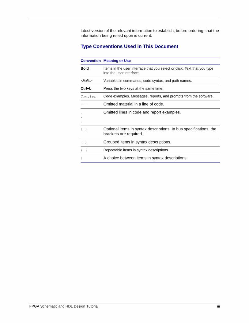
Type Conventions Used in This Document
Convention Meaning or Use
Bold Items in the user interface that you select or click. Text that you type into the user interface.
<Italic> Variables in commands, code syntax, and path names.
Ctrl+L Press the two keys at the same time.
Courier Code examples. Messages, reports, and prompts from the software.
... Omitted material in a line of code.
.
.
.
Omitted lines in code and report examples.
[ ] Optional items in syntax descriptions. In bus specifications, the brackets are required.
( ) Grouped items in syntax descriptions.
{ } Repeatable items in syntax descriptions.
| A choice between items in syntax descriptions.

FPGA Schematic and HDL Design Tutorial iv
FPGA Schematic and HDL Design Tutorial v
Contents
FPGA Schematic and HDL Design Tutorial 1Learning Objectives 2Time to Complete This Tutorial 2System Requirements 2Accessing Online Help 2About the Tutorial Design 2About the Tutorial Data Flow 3Task 1: Create a New Project 3Task 2: Target a Device 5Task 3: Add a New Schematic to the Project 6Task 4: Resize the Schematic Sheet 7Task 5: Add a Title Block for the Schematic Sheet 8Task 6: Create a Verilog Module from a Block Symbol 8Task 7: Create a Block Symbol from IPexpress 11Task 8: Place Symbols from the Lattice FPGA Library 13Task 9: Add Wires 15Task 10: Edit the Schematic 16Task 11: Add Wire Stubs and Duplicate the Output Buffer Circuits 17Task 12: Create Bus Connections 18Task 13: Add Bus Taps with Signal Names 20Task 14: Add Input Net Names 21Task 15: Copy Net Names 22Task 16: Add Data Output Net Names 22Task 17: Add I/O Markers 23Task 18: Create Iterated Instances of the Flip-Flop 24Task 19: Add Net Attributes for sysIO Buffers 25
Contents
FPGA Schematic and HDL Design Tutorial vi
Task 20: Create a Matching Symbol 26Task 21: Check the Schematic for Consistency Errors 27Task 22: Navigate the Design 28Task 23: Push into the COUNTER Block Symbol 28Task 24: Access Connectivity Information for the COUNTER Block 29Task 25: Query a Net 30Task 26: Translate Schematics to HDL 30Task 27: Implement a Schematic-Based Project 32Summary 33Glossary 33Recommended Reference Materials 34

FPGA Schematic and HDL Design Tutorial 1
FPGA Schematic and HDL Design Tutorial
This tutorial leads you through all the basic steps of designing and implementing a counter circuit targeted to the MachXO crossover programmable device family. It shows you how to use several processes, tools, and reports from the ispLEVER software suite to create a top-level schematic and add Verilog HDL source created by the ispLEVER module and IP core program, IPexpress, to the project. The tutorial then proceeds to step through the processes of placing block symbols, library elements, adding wires and buses, and defining net attributes to configure sysIO buffers of the MachXO device.
The ispLEVER software supports mixed-mode design entry: a design with at least one schematic module as the top project source, and one or more sources of the same language. The language sources are mutually exclusive, so you must select one of the three types when you begin a new project. For example, in addition to the schematic, you must select an ABEL-HDL source (CPLD and SPLD devices only), a Verilog HDL source, or a VHDL source.
The schematic design entry environment is a set of tools that allow you to capture the structure of a design as either a flat description or a hierarchical set of components, and the connectivity between these components. Then you can use this description to drive the ispLEVER implementation and verification tools. Schematic designs can be single-level (flat) or multi-level (hierarchical). Schematics can be drawn on multiple “sheets” and be any size.
FPGA Schematic and HDL Design Tutorial Learning Objectives
FPGA Schematic and HDL Design Tutorial 2
Learning ObjectivesWhen you have completed this tutorial, you should be able to do the following:
Set up a Schematic/Verilog HDL project
Add various schematic elements to create a top-level schematic source
Check the schematic for errors
Create a new Verilog HDL source template from a schematic block
Create a schematic symbol from IPexpress
Create a schematic block from a Verilog HDL source file
Add schematic net attributes to define sysIO buffer preferences
Use the Hierarchy Navigator to navigate through the design and examine net connectivity
Produce HDL output for simulation or synthesis
Time to Complete This TutorialThe time to complete this tutorial is about 45 minutes.
System RequirementsOne of the following software configurations is required to complete the tutorial:
ispLEVER-Starter FPGA Module with the ispLEVER-Starter Synplify Synthesis Module
ispLEVER
Accessing Online HelpYou can find online help information on any tool included in the tutorial at any time by pressing the F1 key.
About the Tutorial DesignThe design in this tutorial consists of a top-level schematic, library elements, and two lower level Verilog HDL modules. It uses both a top-down and bottom-up design methodology. The design that you create is targeted to a MachXO crossover programmable logic device.
FPGA Schematic and HDL Design Tutorial About the Tutorial Data Flow
FPGA Schematic and HDL Design Tutorial 3
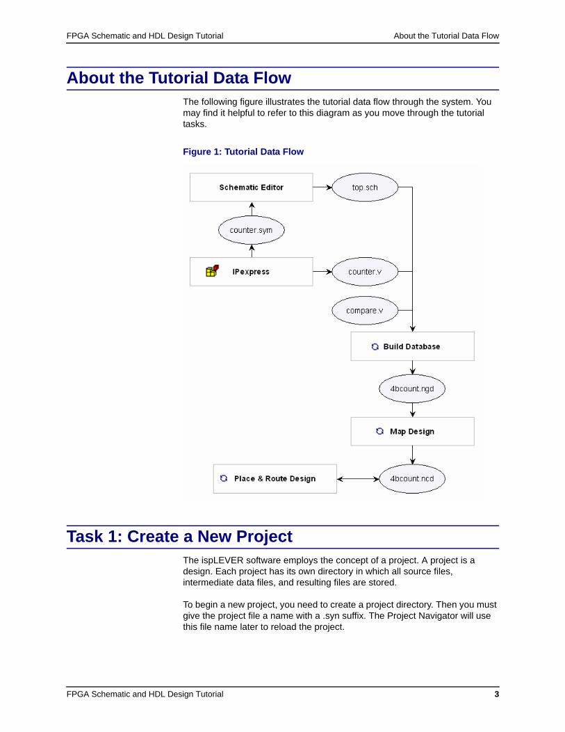
About the Tutorial Data FlowThe following figure illustrates the tutorial data flow through the system. You may find it helpful to refer to this diagram as you move through the tutorial tasks.
Figure 1: Tutorial Data Flow
Task 1: Create a New ProjectThe ispLEVER software employs the concept of a project. A project is a design. Each project has its own directory in which all source files, intermediate data files, and resulting files are stored.
To begin a new project, you need to create a project directory. Then you must give the project file a name with a .syn suffix. The Project Navigator will use this file name later to reload the project.
FPGA Schematic and HDL Design Tutorial Task 1: Create a New Project
FPGA Schematic and HDL Design Tutorial 4
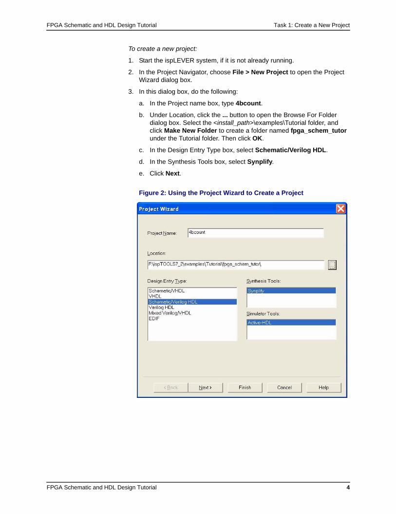
To create a new project:
1. Start the ispLEVER system, if it is not already running.
2. In the Project Navigator, choose File > New Project to open the Project Wizard dialog box.
3. In this dialog box, do the following:
a. In the Project name box, type 4bcount.
b. Under Location, click the ... button to open the Browse For Folder dialog box. Select the <install_path>\examples\Tutorial folder, and click Make New Folder to create a folder named fpga_schem_tutor under the Tutorial folder. Then click OK.
c. In the Design Entry Type box, select Schematic/Verilog HDL.
d. In the Synthesis Tools box, select Synplify.
e. Click Next.
Figure 2: Using the Project Wizard to Create a Project
FPGA Schematic and HDL Design Tutorial Task 2: Target a Device
FPGA Schematic and HDL Design Tutorial 5
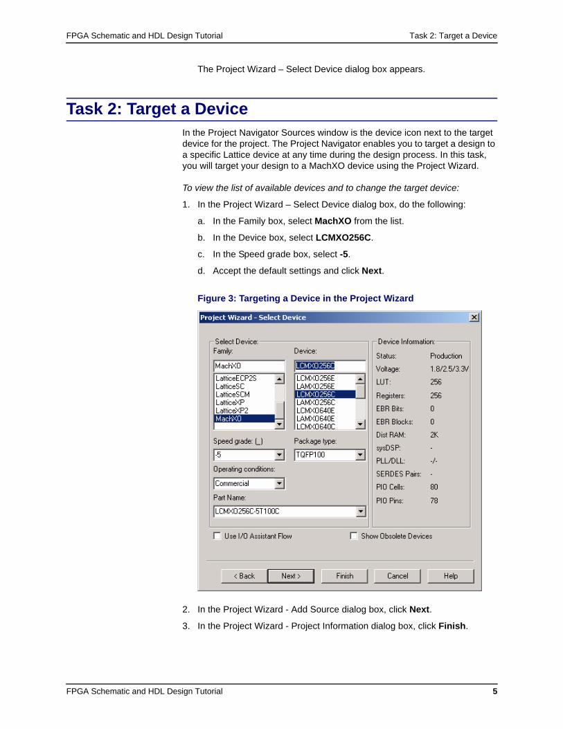
The Project Wizard – Select Device dialog box appears.
Task 2: Target a DeviceIn the Project Navigator Sources window is the device icon next to the target device for the project. The Project Navigator enables you to target a design to a specific Lattice device at any time during the design process. In this task, you will target your design to a MachXO device using the Project Wizard.
To view the list of available devices and to change the target device:
1. In the Project Wizard – Select Device dialog box, do the following:
a. In the Family box, select MachXO from the list.
b. In the Device box, select LCMXO256C.
c. In the Speed grade box, select -5.
d. Accept the default settings and click Next.
Figure 3: Targeting a Device in the Project Wizard
2. In the Project Wizard - Add Source dialog box, click Next.
3. In the Project Wizard - Project Information dialog box, click Finish.

FPGA Schematic and HDL Design Tutorial Task 3: Add a New Schematic to the Project
FPGA Schematic and HDL Design Tutorial 6
Task 3: Add a New Schematic to the ProjectThe schematic design entry environment is a set of tools that enable you to capture the structure of a design as either a flat description or a hierarchical set of components, and the connectivity between these components. Then you can use this description to drive the implementation and verification tools.
You create schematic designs using the Schematic Editor. Schematics can be single-level (flat) or multi-level (hierarchical). Schematics can be drawn on multiple “sheets” and be any size. The Schematic Editor can work in conjunction with the Hierarchy Navigator, Symbol Editor, and Library Manager programs.
Designing top-down, you will first create the top-level source for the project.
To add a new schematic source to the project:
1. In the Project Navigator, choose Source > New to open the New Source dialog box.
2. Select Schematic and click OK.
The Schematic Editor opens and prompts you to enter a file name for the schematic.
3. Type the name top and click OK.
The software imports the schematic into the Project Navigator as a new source file, top.sch.
FPGA Schematic and HDL Design Tutorial Task 4: Resize the Schematic Sheet
FPGA Schematic and HDL Design Tutorial 7
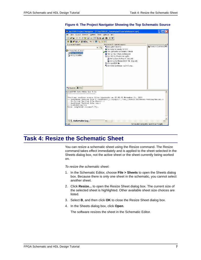
Figure 4: The Project Navigator Showing the Top Schematic Source
Task 4: Resize the Schematic SheetYou can resize a schematic sheet using the Resize command. The Resize command takes effect immediately and is applied to the sheet selected in the Sheets dialog box, not the active sheet or the sheet currently being worked on.
To resize the schematic sheet:
1. In the Schematic Editor, choose File > Sheets to open the Sheets dialog box. Because there is only one sheet in the schematic, you cannot select another sheet.
2. Click Resize... to open the Resize Sheet dialog box. The current size of the selected sheet is highlighted. Other available sheet size choices are listed.
3. Select B, and then click OK to close the Resize Sheet dialog box.
4. In the Sheets dialog box, click Open.
The software resizes the sheet in the Schematic Editor.
FPGA Schematic and HDL Design Tutorial Task 5: Add a Title Block for the Schematic Sheet
FPGA Schematic and HDL Design Tutorial 8
Task 5: Add a Title Block for the Schematic SheetTo help document the schematic, you will add a title block from the Lattice Symbol Library. Title blocks are special non-electrical elements of the schematic that often specifies the author, timestamp, sheet number, revision, and size of the schematic.
To add a title block symbol in the schematic:
1. In the Schematic Editor, choose Add > Symbol to open the Symbol Libraries dialog box.
2. In the dialog box, under Library, select lattice.lib.
3. Under Symbol, scroll down the list and select title_b. The symbol is attached to the cursor.
4. Click anywhere on the schematic page.
The title block symbol snaps to the lower right corner of the schematic page.
5. Close the Symbol Libraries dialog box.
Task 6: Create a Verilog Module from a Block SymbolThe next step in this top-down design is to create a block symbol to represent a lower-level module of the design. The ispLEVER Symbol Editor helps you design the I/O ports of the lower-level Verilog HDL or VHDL sources to match the names of the pins on the corresponding block symbols.
To create a block symbol and Verilog template:
1. In the Schematic Editor, choose Add > New Block Symbol… to open the New Block Symbol dialog box.
2. Specify the following to define the block:
Block Name: COMPARE
Input Pins: =a[3:0]=, =b[3:0]=
Output Pins: aeqb
Note the syntax used with the Input Pins box. If a bus name appears in one of these boxes, it must be enclosed in equal signs (=busname=). If a compound name appears in the pin list and is not surrounded by equal signs, it is expanded to produce individual pins for each name. If the name is enclosed by equal signs, it produces a bus pin.
3. Click Edit.
Tip
If you do not see a grid, choose Options > Preferences and select Display Grid.

FPGA Schematic and HDL Design Tutorial Task 6: Create a Verilog Module from a Block Symbol
FPGA Schematic and HDL Design Tutorial 9
The Schematic Editor creates the compare symbol, compare.sym, in the project directory, and then opens the Symbol Editor with the new block symbol loaded.
The Symbol Editor provides several tools to create graphical schematic symbols. When used in this manner as a top-down block diagram tool, you will often use the Symbol Editor to position pins to create an easy-to-read data flow on the schematic.
4. In the Symbol Editor, choose File > Verilog Template.
The Symbol Editor generates a notice that the file has been generated. Click OK to close the notice.
5. Choose File > Exit to exit the Symbol Editor.
To add the COMPARE block symbol in the schematic:
1. In the Schematic Editor, choose Add > Symbol to open the Symbol Libraries dialog box.
2. In the dialog box, under Library, select (Local).
3. Under Symbol, select compare. The symbol is attached to the cursor.
4. Position the cursor slightly above the upper middle area of the schematic, and then click to place the symbol.
5. Close the Symbol Libraries dialog box.
6. Choose File > Save.
The Schematic Editor assigns an Instance Name to the COMPARE block symbol and saves the schematic (top.sch).
To add the Verilog HDL module to the project:
1. Select the Project Navigator.
Notice the Modules tab of the Sources in Project window now shows [top (top.sch)] as the root of the design and a reference to the COMPARE
Note
You should use naming conventions that comply with Verilog HDL or VHDL standards and avoid special characters.
Note
While the Schematic Editor displays upper and lower case names, you should consider the HDL output from the Schematic Editor case insensitive and assume that all net and symbol names will be written in lower-case.
Tip
If you do not see a grid, choose Options > Preferences and select Display Grid.
Tip
If you make a mistake placing a symbol, you can choose Edit > Cut or Move, and then click the symbol that is to receive the action.
FPGA Schematic and HDL Design Tutorial Task 6: Create a Verilog Module from a Block Symbol
FPGA Schematic and HDL Design Tutorial 10
module. This illustrates the reference to COMPARE implied by the instantiation of the new block symbol.
Remember you have generated a Verilog HDL template for the COMPARE symbol in the Symbol Editor. Next you will import the template into the project and edit the contents.
2. In the Project Navigator, choose Source > Import to open the Import File dialog box.
3. In the dialog box, select compare.v and click Open.
The Import Source Type dialog box appears.
4. Select Verilog Module and click OK.
The Verilog template is added to the project. A new branch of the file hierarchy is established as compare (compare.v).
5. Double-click compare (compare.v).
The Text Editor opens with the compare.v file loaded.
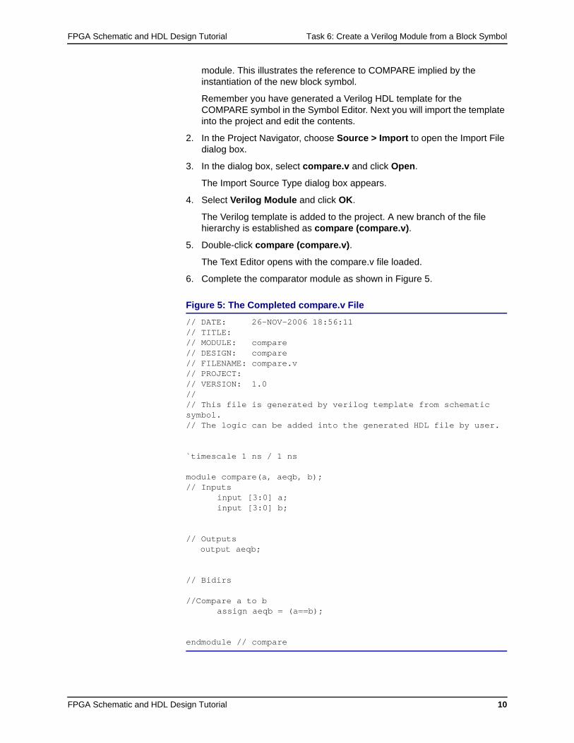
6. Complete the comparator module as shown in Figure 5.
Figure 5: The Completed compare.v File
// DATE: 26-NOV-2006 18:56:11 // TITLE: // MODULE: compare// DESIGN: compare// FILENAME: compare.v// PROJECT: // VERSION: 1.0//// This file is generated by verilog template from schematic symbol.// The logic can be added into the generated HDL file by user.
`timescale 1 ns / 1 ns
module compare(a, aeqb, b);// Inputs
input [3:0] a;input [3:0] b;
// Outputs output aeqb;
// Bidirs
//Compare a to bassign aeqb = (a==b);
endmodule // compare
FPGA Schematic and HDL Design Tutorial Task 7: Create a Block Symbol from IPexpress
FPGA Schematic and HDL Design Tutorial 11
7. Choose File > Save All.
8. Choose File > Exit.
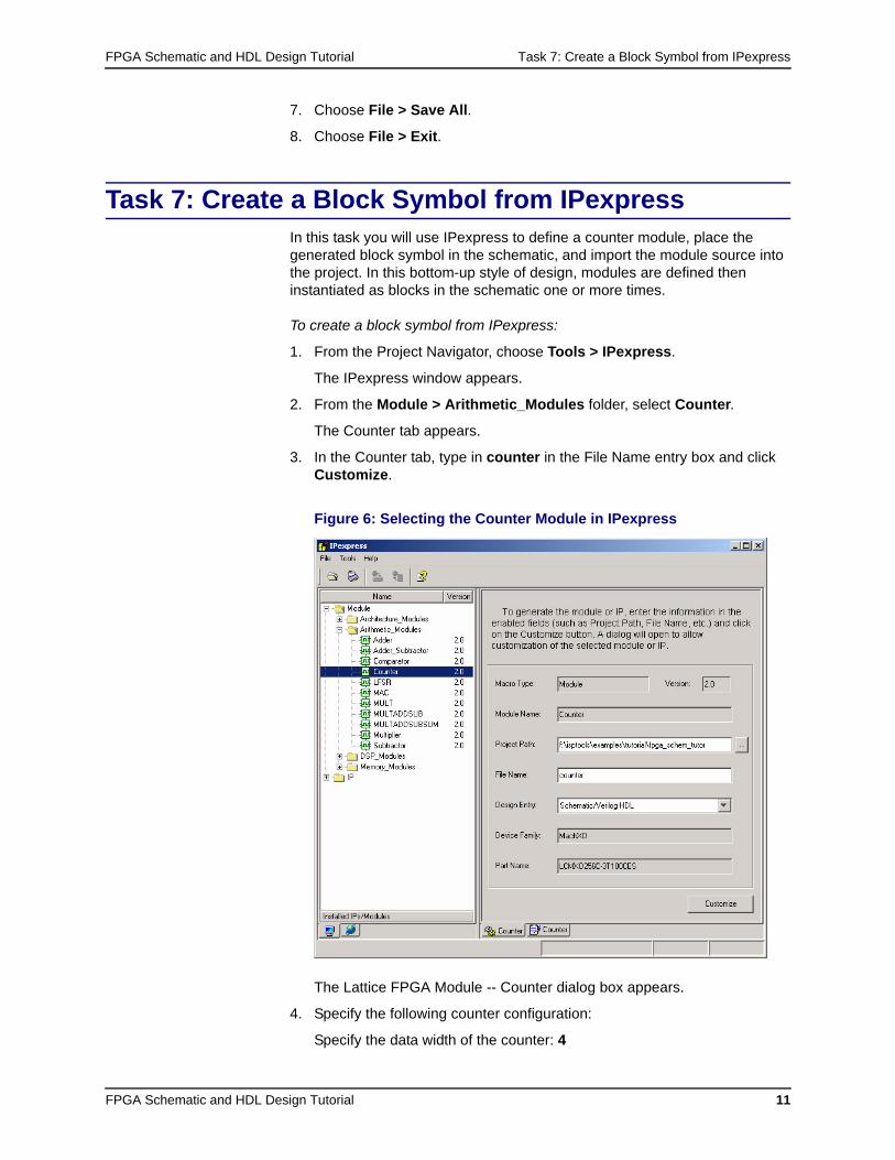
Task 7: Create a Block Symbol from IPexpressIn this task you will use IPexpress to define a counter module, place the generated block symbol in the schematic, and import the module source into the project. In this bottom-up style of design, modules are defined then instantiated as blocks in the schematic one or more times.
To create a block symbol from IPexpress:
1. From the Project Navigator, choose Tools > IPexpress.
The IPexpress window appears.
2. From the Module > Arithmetic_Modules folder, select Counter.
The Counter tab appears.
3. In the Counter tab, type in counter in the File Name entry box and click Customize.
Figure 6: Selecting the Counter Module in IPexpress
The Lattice FPGA Module -- Counter dialog box appears.
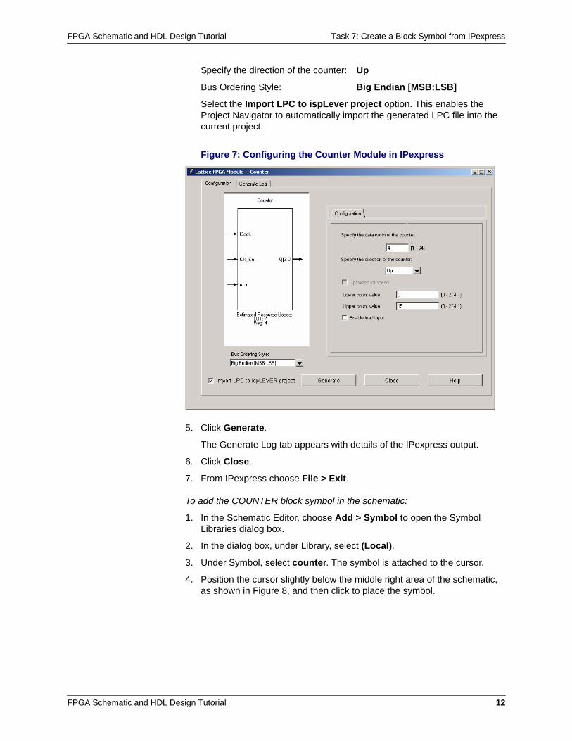
4. Specify the following counter configuration:
Specify the data width of the counter: 4
FPGA Schematic and HDL Design Tutorial Task 7: Create a Block Symbol from IPexpress
FPGA Schematic and HDL Design Tutorial 12
Specify the direction of the counter: Up
Bus Ordering Style: Big Endian [MSB:LSB]
Select the Import LPC to ispLever project option. This enables the Project Navigator to automatically import the generated LPC file into the current project.
Figure 7: Configuring the Counter Module in IPexpress
5. Click Generate.
The Generate Log tab appears with details of the IPexpress output.
6. Click Close.
7. From IPexpress choose File > Exit.
To add the COUNTER block symbol in the schematic:
1. In the Schematic Editor, choose Add > Symbol to open the Symbol Libraries dialog box.
2. In the dialog box, under Library, select (Local).
3. Under Symbol, select counter. The symbol is attached to the cursor.
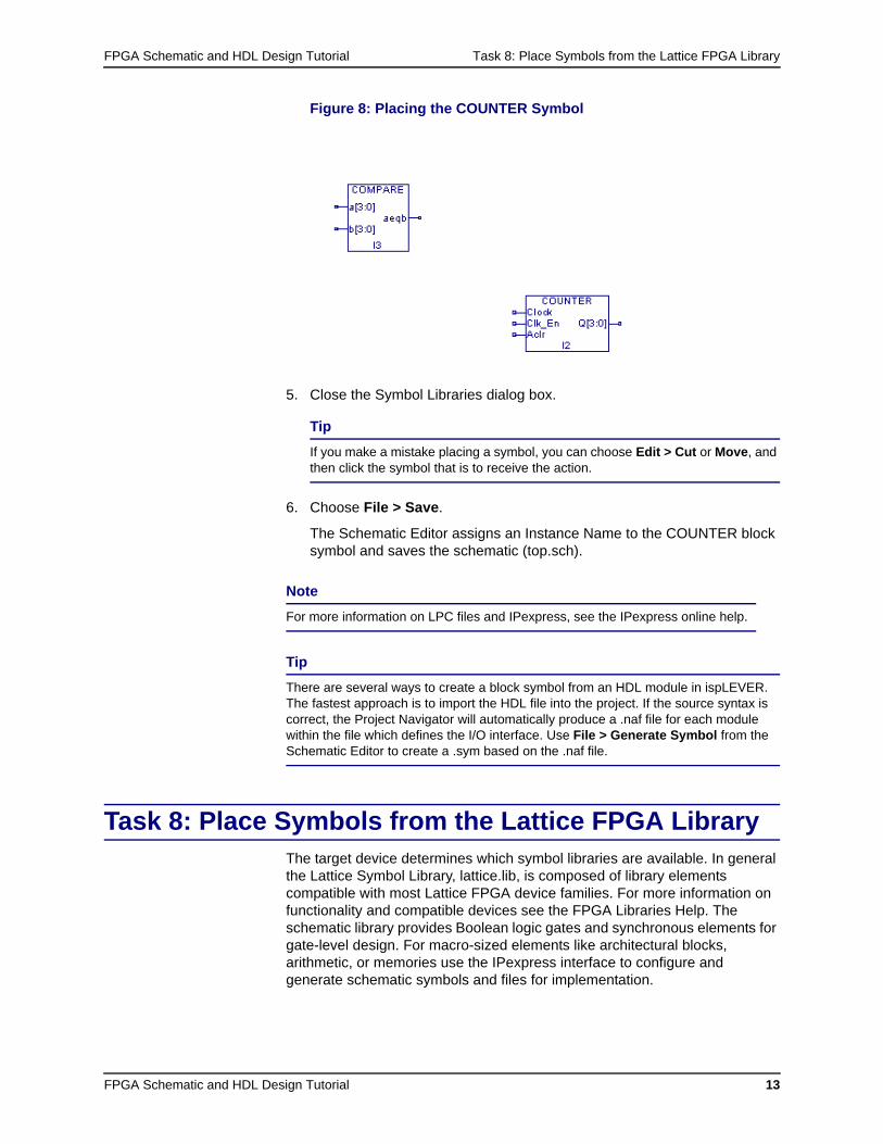
4. Position the cursor slightly below the middle right area of the schematic, as shown in Figure 8, and then click to place the symbol.
FPGA Schematic and HDL Design Tutorial Task 8: Place Symbols from the Lattice FPGA Library
FPGA Schematic and HDL Design Tutorial 13
Figure 8: Placing the COUNTER Symbol
5. Close the Symbol Libraries dialog box.
6. Choose File > Save.
The Schematic Editor assigns an Instance Name to the COUNTER block symbol and saves the schematic (top.sch).
Task 8: Place Symbols from the Lattice FPGA LibraryThe target device determines which symbol libraries are available. In general the Lattice Symbol Library, lattice.lib, is composed of library elements compatible with most Lattice FPGA device families. For more information on functionality and compatible devices see the FPGA Libraries Help. The schematic library provides Boolean logic gates and synchronous elements for gate-level design. For macro-sized elements like architectural blocks, arithmetic, or memories use the IPexpress interface to configure and generate schematic symbols and files for implementation.
Tip
If you make a mistake placing a symbol, you can choose Edit > Cut or Move, and then click the symbol that is to receive the action.
Note
For more information on LPC files and IPexpress, see the IPexpress online help.
Tip
There are several ways to create a block symbol from an HDL module in ispLEVER. The fastest approach is to import the HDL file into the project. If the source syntax is correct, the Project Navigator will automatically produce a .naf file for each module within the file which defines the I/O interface. Use File > Generate Symbol from the Schematic Editor to create a .sym based on the .naf file.

FPGA Schematic and HDL Design Tutorial Task 8: Place Symbols from the Lattice FPGA Library
FPGA Schematic and HDL Design Tutorial 14
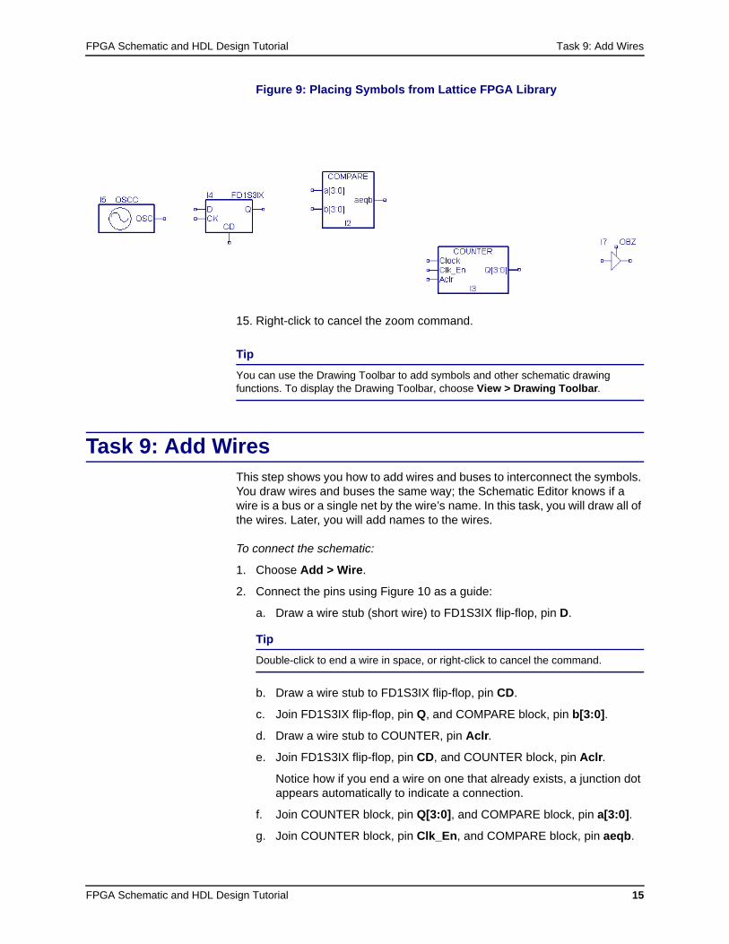
To place symbols from the Lattice symbol library:
1. In the Schematic Editor, choose Add > Symbol.
2. In the Symbol Libraries dialog box, under Library, select lattice.lib.
3. Under Symbol, scroll down the list and select fd1s3ix. The symbol is attached to the cursor.
FD1S3IX is a positive edge triggered D flip-flop with positive level synchronous clear.
4. Place the symbol so that the FD1S3IX flip-flop symbol’s output is aligned with the b[3:0] input pin on the COMPARE block symbol.
5. In the Symbol Libraries dialog box, under Library, select lattice.lib.
6. Under Symbol, select oscc. The symbol is attached to the cursor.
OSCC represents the internal CMOS oscillator of the MachXO device family.
7. Place the symbol so that the OSCC symbol’s output is aligned with the CK input pin on the FD1S3IX flip-flop symbol.
8. In the Symbol Libraries dialog box, under Library, select lattice.lib.
9. Under Symbol, select obz. The symbol is attached to the cursor.
OBZ is an output buffer with tristate.
10. Place the symbol so that the OBZ symbol’s input is placed one or two grid positions above Q[3:0] output pin on the COUNTER block symbol.
11. Close the Symbol Libraries dialog box.
12. Choose File > Save.
The Schematic Editor assigns Instance Names to the newly-added symbols and saves the schematic (top.sch).
13. Choose View > Zoom In. The cursor changes to a large Z.
14. Click a portion of the schematic to enlarge it to a readable size. Or drag an area to zoom in to a view similar to Figure 9.
Note
The spacing of symbols in the schematic is very important. If symbols are placed too close to each other, you will not be able to add wires, bus taps, and so forth between the symbols. In this step, make sure the horizontal distance between the OSCC symbol and FDIS3IX flip-flop symbol is equal to at least the width of the OSCC symbol (see Figure 9).
FPGA Schematic and HDL Design Tutorial Task 9: Add Wires
FPGA Schematic and HDL Design Tutorial 15
Figure 9: Placing Symbols from Lattice FPGA Library
15. Right-click to cancel the zoom command.
Task 9: Add WiresThis step shows you how to add wires and buses to interconnect the symbols. You draw wires and buses the same way; the Schematic Editor knows if a wire is a bus or a single net by the wire’s name. In this task, you will draw all of the wires. Later, you will add names to the wires.
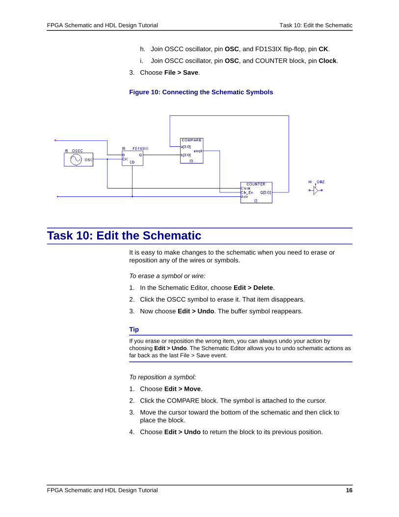
To connect the schematic:
1. Choose Add > Wire.
2. Connect the pins using Figure 10 as a guide:
a. Draw a wire stub (short wire) to FD1S3IX flip-flop, pin D.
b. Draw a wire stub to FD1S3IX flip-flop, pin CD.
c. Join FD1S3IX flip-flop, pin Q, and COMPARE block, pin b[3:0].
d. Draw a wire stub to COUNTER, pin Aclr.
e. Join FD1S3IX flip-flop, pin CD, and COUNTER block, pin Aclr.
Notice how if you end a wire on one that already exists, a junction dot appears automatically to indicate a connection.
f. Join COUNTER block, pin Q[3:0], and COMPARE block, pin a[3:0].
g. Join COUNTER block, pin Clk_En, and COMPARE block, pin aeqb.
Tip
You can use the Drawing Toolbar to add symbols and other schematic drawing functions. To display the Drawing Toolbar, choose View > Drawing Toolbar.
Tip
Double-click to end a wire in space, or right-click to cancel the command.
FPGA Schematic and HDL Design Tutorial Task 10: Edit the Schematic
FPGA Schematic and HDL Design Tutorial 16
h. Join OSCC oscillator, pin OSC, and FD1S3IX flip-flop, pin CK.
i. Join OSCC oscillator, pin OSC, and COUNTER block, pin Clock.
3. Choose File > Save.
Figure 10: Connecting the Schematic Symbols
Task 10: Edit the SchematicIt is easy to make changes to the schematic when you need to erase or reposition any of the wires or symbols.
To erase a symbol or wire:
1. In the Schematic Editor, choose Edit > Delete.
2. Click the OSCC symbol to erase it. That item disappears.
3. Now choose Edit > Undo. The buffer symbol reappears.
To reposition a symbol:
1. Choose Edit > Move.
2. Click the COMPARE block. The symbol is attached to the cursor.
3. Move the cursor toward the bottom of the schematic and then click to place the block.
4. Choose Edit > Undo to return the block to its previous position.
Tip
If you erase or reposition the wrong item, you can always undo your action by choosing Edit > Undo. The Schematic Editor allows you to undo schematic actions as far back as the last File > Save event.
FPGA Schematic and HDL Design Tutorial Task 11: Add Wire Stubs and Duplicate the Output Buffer
FPGA Schematic and HDL Design Tutorial 17
To reposition several items at once:
1. Choose Edit > Move.
2. Drag a square around both the COMPARE block and the FD1S3IX flip-flop. Both items are attached to the cursor.
3. Move the cursor to the bottom portion of the schematic and click to place the items.
4. Choose Edit > Undo to return the items to their previous positions.
To reposition a symbol but retain connectivity:
1. Choose Edit > Drag.
2. Click the COMPARE block. The symbol is attached to the cursor.
3. Move the cursor to the bottom portion of the schematic and click to place the block.
Notice the wire connection rubber bands to maintain a connection.
4. Choose Edit > Undo to return the block to its previous position.
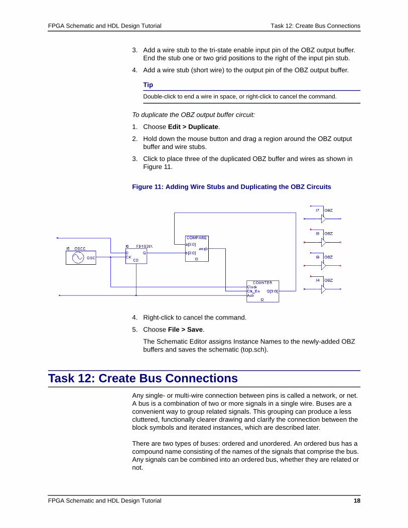
Task 11: Add Wire Stubs and Duplicate the Output Buffer Circuits
This step shows you how to use the Duplicate command to quickly add the rest of the output buffers. The Duplicate command lets you copy one or more elements, and then place them at different locations within the same symbol or schematic. You can place the duplicated item as many times as you want until you select another command. Duplicate differs from the Copy/Paste command sequence only in that it does not change the contents of the clipboard.
To add wire stubs:
1. Choose Add > Wire.
2. Click the input pin of the OBZ output buffer symbol. Move the cursor to the left to create a horizontal segment with a length equal to about half the horizontal distance between the wire driven by the COUNTER block and the OBZ output buffer. Click once to end the segment.
Note
During a Drag operation, the Schematic Editor prevents you from crossing wire or bus connection that would change the network.
Tip
Almost all commands remain in effect until you select a different command. For example, if the Add Wire command is active, you can continue to draw wires until you select a different command. You can also right-click to cancel a command.
FPGA Schematic and HDL Design Tutorial Task 12: Create Bus Connections
FPGA Schematic and HDL Design Tutorial 18
3. Add a wire stub to the tri-state enable input pin of the OBZ output buffer. End the stub one or two grid positions to the right of the input pin stub.
4. Add a wire stub (short wire) to the output pin of the OBZ output buffer.
To duplicate the OBZ output buffer circuit:
1. Choose Edit > Duplicate.
2. Hold down the mouse button and drag a region around the OBZ output buffer and wire stubs.
3. Click to place three of the duplicated OBZ buffer and wires as shown in Figure 11.
Figure 11: Adding Wire Stubs and Duplicating the OBZ Circuits
4. Right-click to cancel the command.
5. Choose File > Save.
The Schematic Editor assigns Instance Names to the newly-added OBZ buffers and saves the schematic (top.sch).
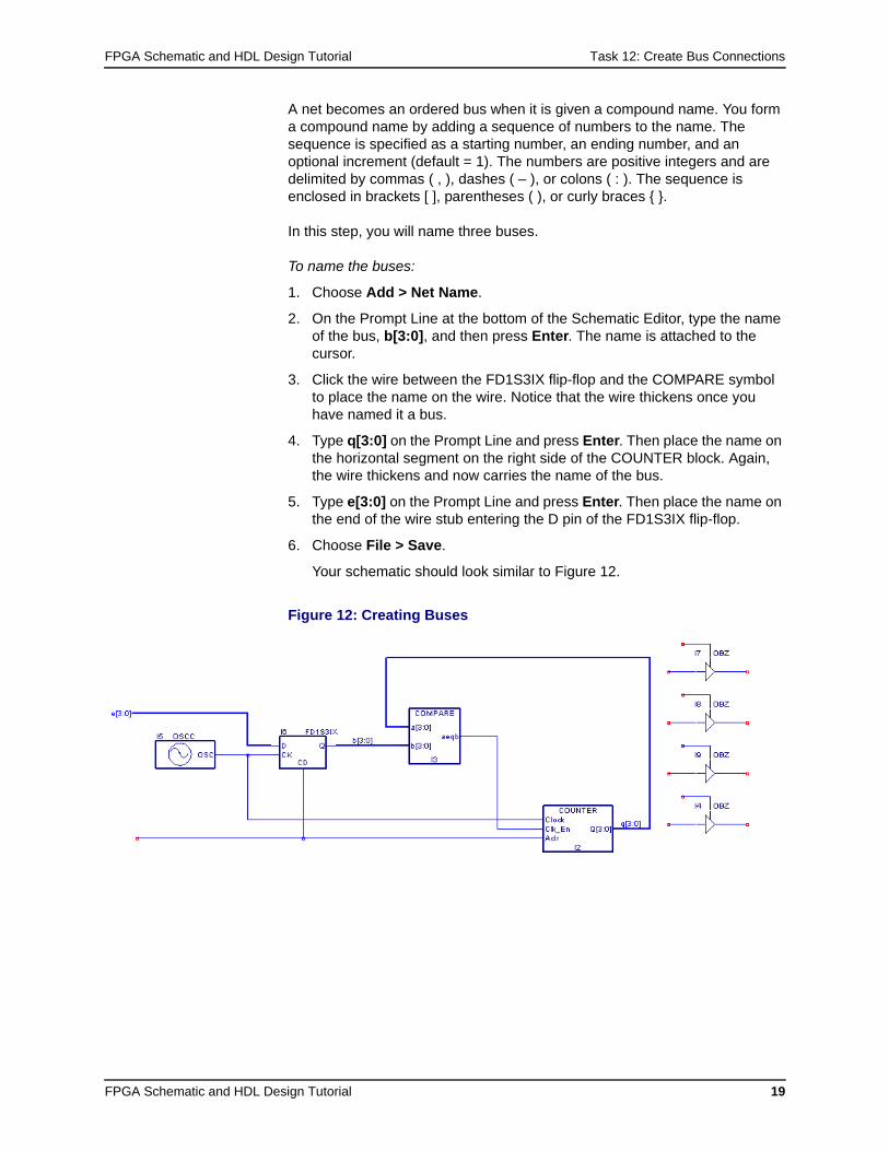
Task 12: Create Bus ConnectionsAny single- or multi-wire connection between pins is called a network, or net. A bus is a combination of two or more signals in a single wire. Buses are a convenient way to group related signals. This grouping can produce a less cluttered, functionally clearer drawing and clarify the connection between the block symbols and iterated instances, which are described later.
There are two types of buses: ordered and unordered. An ordered bus has a compound name consisting of the names of the signals that comprise the bus. Any signals can be combined into an ordered bus, whether they are related or not.
Tip
Double-click to end a wire in space, or right-click to cancel the command.
FPGA Schematic and HDL Design Tutorial Task 12: Create Bus Connections
FPGA Schematic and HDL Design Tutorial 19
A net becomes an ordered bus when it is given a compound name. You form a compound name by adding a sequence of numbers to the name. The sequence is specified as a starting number, an ending number, and an optional increment (default = 1). The numbers are positive integers and are delimited by commas ( , ), dashes ( – ), or colons ( : ). The sequence is enclosed in brackets [ ], parentheses ( ), or curly braces { }.
In this step, you will name three buses.
To name the buses:
1. Choose Add > Net Name.
2. On the Prompt Line at the bottom of the Schematic Editor, type the name of the bus, b[3:0], and then press Enter. The name is attached to the cursor.
3. Click the wire between the FD1S3IX flip-flop and the COMPARE symbol to place the name on the wire. Notice that the wire thickens once you have named it a bus.
4. Type q[3:0] on the Prompt Line and press Enter. Then place the name on the horizontal segment on the right side of the COUNTER block. Again, the wire thickens and now carries the name of the bus.
5. Type e[3:0] on the Prompt Line and press Enter. Then place the name on the end of the wire stub entering the D pin of the FD1S3IX flip-flop.
6. Choose File > Save.
Your schematic should look similar to Figure 12.
Figure 12: Creating Buses
FPGA Schematic and HDL Design Tutorial Task 13: Add Bus Taps with Signal Names
FPGA Schematic and HDL Design Tutorial 20
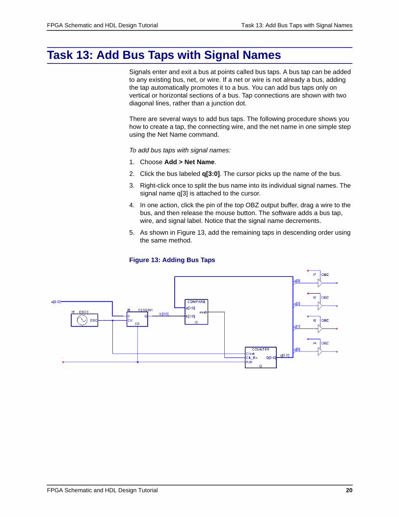
Task 13: Add Bus Taps with Signal NamesSignals enter and exit a bus at points called bus taps. A bus tap can be added to any existing bus, net, or wire. If a net or wire is not already a bus, adding the tap automatically promotes it to a bus. You can add bus taps only on vertical or horizontal sections of a bus. Tap connections are shown with two diagonal lines, rather than a junction dot.
There are several ways to add bus taps. The following procedure shows you how to create a tap, the connecting wire, and the net name in one simple step using the Net Name command.
To add bus taps with signal names:
1. Choose Add > Net Name.
2. Click the bus labeled q[3:0]. The cursor picks up the name of the bus.
3. Right-click once to split the bus name into its individual signal names. The signal name q[3] is attached to the cursor.
4. In one action, click the pin of the top OBZ output buffer, drag a wire to the bus, and then release the mouse button. The software adds a bus tap, wire, and signal label. Notice that the signal name decrements.
5. As shown in Figure 13, add the remaining taps in descending order using the same method.
Figure 13: Adding Bus Taps
FPGA Schematic and HDL Design Tutorial Task 14: Add Input Net Names
FPGA Schematic and HDL Design Tutorial 21
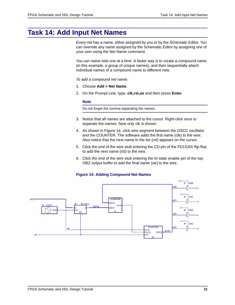
Task 14: Add Input Net NamesEvery net has a name, either assigned by you or by the Schematic Editor. You can override any name assigned by the Schematic Editor by assigning one of your own using the Net Name command.
You can name nets one at a time. A faster way is to create a compound name (in this example, a group of unique names), and then sequentially attach individual names of a compound name to different nets.
To add a compound net name:
1. Choose Add > Net Name.
2. On the Prompt Line, type: clk,rst,oe and then press Enter.
3. Notice that all names are attached to the cursor. Right-click once to separate the names. Now only clk is shown.
4. As shown in Figure 14, click wire segment between the OSCC oscillator and the COUNTER. The software adds the first name (clk) to the wire. Also notice that the next name in the list (rst) appears on the cursor.
5. Click the end of the wire stub entering the CD pin of the FD1S3IX flip-flop to add the next name (rst) to the wire.
6. Click the end of the wire stub entering the tri-state enable pin of the top OBZ output buffer to add the final name (oe) to the wire.
Figure 14: Adding Compound Net Names
Note
Do not forget the comma separating the names.
FPGA Schematic and HDL Design Tutorial Task 15: Copy Net Names
FPGA Schematic and HDL Design Tutorial 22
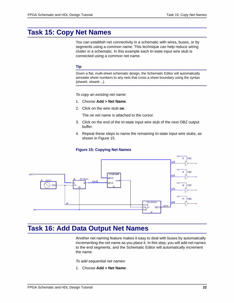
Task 15: Copy Net NamesYou can establish net connectivity in a schematic with wires, buses, or by segments using a common name. This technique can help reduce wiring clutter in a schematic. In this example each tri-state input wire stub is connected using a common net name.
To copy an existing net name:
1. Choose Add > Net Name.
2. Click on the wire stub oe.
The oe net name is attached to the cursor.
3. Click on the end of the tri-state input wire stub of the next OBZ output buffer.
4. Repeat these steps to name the remaining tri-state input wire stubs, as shown in Figure 15.
Figure 15: Copying Net Names
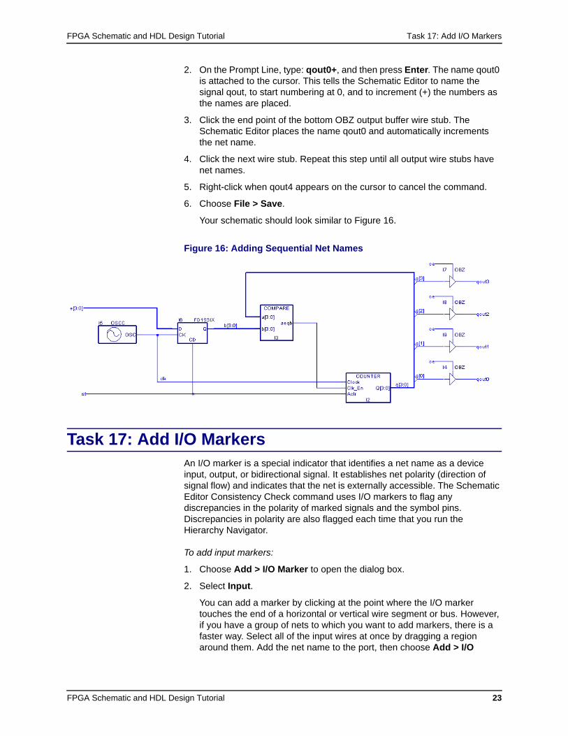
Task 16: Add Data Output Net NamesAnother net naming feature makes it easy to deal with buses by automatically incrementing the net name as you place it. In this step, you will add net names to the end segments, and the Schematic Editor will automatically increment the name.
To add sequential net names:
1. Choose Add > Net Name.
Tip
Given a flat, multi-sheet schematic design, the Schematic Editor will automatically annotate sheet numbers to any nets that cross a sheet boundary using the syntax {sheet#, sheet#…}.
FPGA Schematic and HDL Design Tutorial Task 17: Add I/O Markers
FPGA Schematic and HDL Design Tutorial 23
2. On the Prompt Line, type: qout0+, and then press Enter. The name qout0 is attached to the cursor. This tells the Schematic Editor to name the signal qout, to start numbering at 0, and to increment (+) the numbers as the names are placed.
3. Click the end point of the bottom OBZ output buffer wire stub. The Schematic Editor places the name qout0 and automatically increments the net name.
4. Click the next wire stub. Repeat this step until all output wire stubs have net names.
5. Right-click when qout4 appears on the cursor to cancel the command.
6. Choose File > Save.
Your schematic should look similar to Figure 16.
Figure 16: Adding Sequential Net Names
Task 17: Add I/O MarkersAn I/O marker is a special indicator that identifies a net name as a device input, output, or bidirectional signal. It establishes net polarity (direction of signal flow) and indicates that the net is externally accessible. The Schematic Editor Consistency Check command uses I/O markers to flag any discrepancies in the polarity of marked signals and the symbol pins. Discrepancies in polarity are also flagged each time that you run the Hierarchy Navigator.
To add input markers:
1. Choose Add > I/O Marker to open the dialog box.
2. Select Input.
You can add a marker by clicking at the point where the I/O marker touches the end of a horizontal or vertical wire segment or bus. However, if you have a group of nets to which you want to add markers, there is a faster way. Select all of the input wires at once by dragging a region around them. Add the net name to the port, then choose Add > I/O
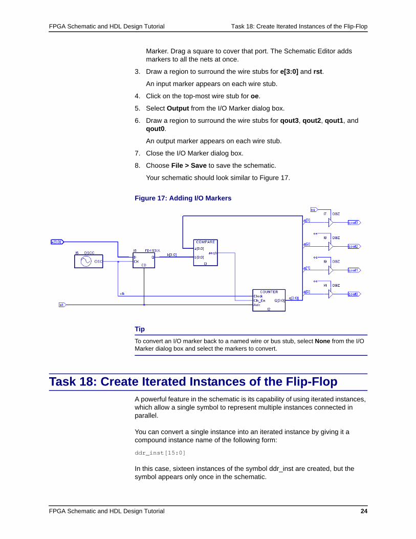
FPGA Schematic and HDL Design Tutorial Task 18: Create Iterated Instances of the Flip-Flop
FPGA Schematic and HDL Design Tutorial 24
Marker. Drag a square to cover that port. The Schematic Editor adds markers to all the nets at once.
3. Draw a region to surround the wire stubs for e[3:0] and rst.
An input marker appears on each wire stub.
4. Click on the top-most wire stub for oe.
5. Select Output from the I/O Marker dialog box.
6. Draw a region to surround the wire stubs for qout3, qout2, qout1, and qout0.
An output marker appears on each wire stub.
7. Close the I/O Marker dialog box.
8. Choose File > Save to save the schematic.
Your schematic should look similar to Figure 17.
Figure 17: Adding I/O Markers
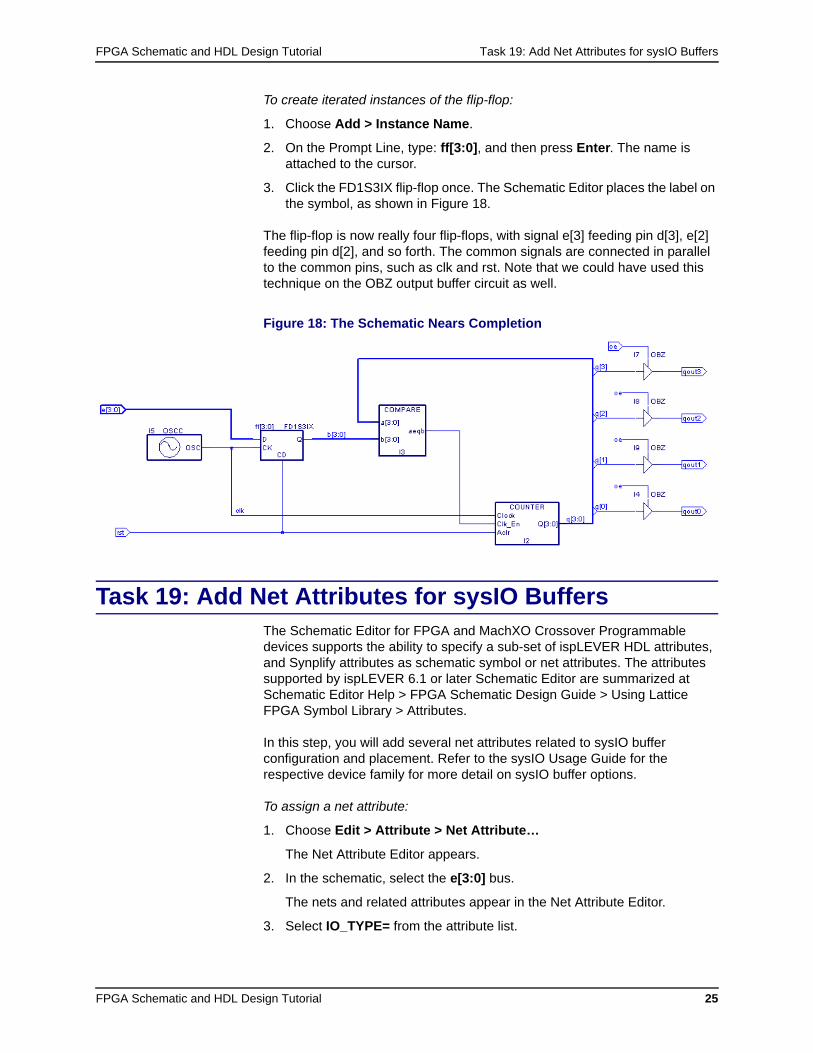
Task 18: Create Iterated Instances of the Flip-FlopA powerful feature in the schematic is its capability of using iterated instances, which allow a single symbol to represent multiple instances connected in parallel.
You can convert a single instance into an iterated instance by giving it a compound instance name of the following form:
ddr_inst[15:0]
In this case, sixteen instances of the symbol ddr_inst are created, but the symbol appears only once in the schematic.
Tip
To convert an I/O marker back to a named wire or bus stub, select None from the I/O Marker dialog box and select the markers to convert.
FPGA Schematic and HDL Design Tutorial Task 19: Add Net Attributes for sysIO Buffers
FPGA Schematic and HDL Design Tutorial 25
To create iterated instances of the flip-flop:
1. Choose Add > Instance Name.
2. On the Prompt Line, type: ff[3:0], and then press Enter. The name is attached to the cursor.
3. Click the FD1S3IX flip-flop once. The Schematic Editor places the label on the symbol, as shown in Figure 18.
The flip-flop is now really four flip-flops, with signal e[3] feeding pin d[3], e[2] feeding pin d[2], and so forth. The common signals are connected in parallel to the common pins, such as clk and rst. Note that we could have used this technique on the OBZ output buffer circuit as well.
Figure 18: The Schematic Nears Completion
Task 19: Add Net Attributes for sysIO BuffersThe Schematic Editor for FPGA and MachXO Crossover Programmable devices supports the ability to specify a sub-set of ispLEVER HDL attributes, and Synplify attributes as schematic symbol or net attributes. The attributes supported by ispLEVER 6.1 or later Schematic Editor are summarized at Schematic Editor Help > FPGA Schematic Design Guide > Using Lattice FPGA Symbol Library > Attributes.
In this step, you will add several net attributes related to sysIO buffer configuration and placement. Refer to the sysIO Usage Guide for the respective device family for more detail on sysIO buffer options.
To assign a net attribute:
1. Choose Edit > Attribute > Net Attribute…
The Net Attribute Editor appears.
2. In the schematic, select the e[3:0] bus.
The nets and related attributes appear in the Net Attribute Editor.
3. Select IO_TYPE= from the attribute list.
FPGA Schematic and HDL Design Tutorial Task 20: Create a Matching Symbol
FPGA Schematic and HDL Design Tutorial 26
4. In the edit box, type in LVCMOS12 and press Enter.
All members of the e[3:0] bus are assigned IO_TYPE=LVCMOS12.
5. Select e[3] from the Net list and select LOC= in the attribute list.
6. In the edit box, type in 81 and press Enter.
A PAD site location for the TQFP100 package is assigned to the bus element e[3].
7. Set the following additional net attributes:
a. e[2]: LOC=80.
b. e[1]: LOC=79.
c. e[0]: LOC=78.
d. rst: LOC=86, IO_TYPE=LVCMOS12.
e. oe: LOC=85, IO_TYPE=LVCMOS12.
8. In the schematic, select a region to encompass the output ports qout3 through qout0.
The four nets and related attributes are displayed in the Net Attribute Editor.
9. Select IO_TYPE= from the attribute list.
10. In the edit box, type in LVCMOS12 and press Enter.
All nets are assigned IO_TYPE=LVCMOS12.
11. Set the following net attributes:
a. qout3: LOC=97.
b. qout2: LOC=96.
c. qout1: LOC=95.
d. qout0: LOC=94.
12. Close the Net Attribute Editor dialog.
13. Choose File > Save.
Task 20: Create a Matching SymbolYou can use the Matching Symbol command to create a symbol file (*.sym) for the schematic currently loaded, with the same base name. The input and output pins on the symbol have the same signal names and polarities as the I/O markers in the schematic.
The Schematic Editor creates the symbol in the same directory as the schematic. You can use the Add Symbol command to insert the symbol into any other schematic. In this bottom-up approach to design you can quickly step and repeat circuits.
In this step, you will create a symbol for the top schematic. The symbol will be saved in the Local symbol library in the project directory.

FPGA Schematic and HDL Design Tutorial Task 21: Check the Schematic for Consistency Errors
FPGA Schematic and HDL Design Tutorial 27
To create a matching symbol for the Top schematic:
1. Choose File > Matching Symbol. The Schematic Editor automatically creates a symbol.
2. Choose Add > Symbol to open the Symbol Libraries dialog box.
3. Under Library, select (Local). Notice, without selecting it, the symbol named top.
4. Close the Symbol Libraries dialog box.
Task 21: Check the Schematic for Consistency ErrorsThe Schematic Editor continually checks for errors, such as closed loops and shorted nets, while you are drawing your schematic. You can also check your schematic for other errors such as unconnected wires or pins or an unnamed signal tapped from a bus. Errors found are shown in a “hot” list box. Clicking an error causes the cursor to jump to its location.
To check for consistency errors:
1. Choose DRC > Consistency Check to open the Error Report. There should be no errors in the report.
2. Close the Error Report.
3. Choose File > Save.
4. Choose Edit > Delete.
5. Drag the area around the circuitry on the OBZ output buffers and output modules of the far right side of the schematic, and then release the mouse button.
6. Choose DRC > Consistency Check again
7. In the Error Report, select an error. Notice that the schematic view shifts to the location of the selected error. Note the Symbol vs. Schematic section of the report. This indicates any inconsistencies between the schematic symbol pins and the I/O markers for the top-level schematic. In a multi-page hierarchical design this is a quick way to detect invalid hierarchical connections.
8. Close the Error Report.
9. Choose File > Exit to exit the schematic. When asked to save your changes, click NO.
You have just created and checked a top-level schematic.
FPGA Schematic and HDL Design Tutorial Task 22: Navigate the Design
FPGA Schematic and HDL Design Tutorial 28
Task 22: Navigate the DesignThe Hierarchy Navigator program allows you to navigate through a schematic design that consists of a top-level schematic, lower-level schematics, and HDL modules. The Hierarchy Navigator loads a full hierarchical design all at once so that you can view it in its complete form, rather than as individual sources. Every schematic sheet and behavioral file at all levels of hierarchy is included.
You can open the Hierarchy Navigator from within the Project Navigator. The Hierarchy Navigator performs several important functions:
It verifies the correctness and consistency of a design’s wiring. Verification occurs at each level in the design, and across all the levels, from top to bottom.
It provides the environment in which you can analyze and optimize the circuit’s performance.
It prepares the design data for later steps in the design process, for example, creating netlists.
To open the Hierarchy Navigator:
1. Select the Project Navigator.
2. In the Modules tab of the Sources in Project window, select [top (top.sch)]. Notice that the Navigate Hierarchy process is displayed at the top of the Processes for current source window. Also notice that Navigate Hierarchy is visible only when a schematic source is selected.
3. In the Processes for current source window, double-click Navigate Hierarchy.
4. The Hierarchy Navigator opens with sheet 1 of the selected schematic source loaded.
Task 23: Push into the COUNTER Block SymbolYou can use the Push/Pop command on the View menu to move down and up (respectively) through the hierarchical levels of a design. This command works on schematics, LPC files created by IPexpress, and HDL-based modules.
You may want to use the Zoom In command to view the COUNTER module before starting this step. Right-click to cancel the zoom command.
Note
You cannot edit the schematic or one of its symbols in the Hierarchy Navigator. However, you can open editors from the Hierarchy Navigator to make changes to a specific schematic element.
FPGA Schematic and HDL Design Tutorial Task 24: Access Connectivity Information for the
FPGA Schematic and HDL Design Tutorial 29
To push into the COUNTER block symbol:
1. Choose View > Push/Pop. The cursor changes to a crosshair.
2. To move down a level into the COUNTER module, click inside the COUNTER schematic symbol.
3. The Text Editor opens with the LPC file description of the module. The LPC file contains the details for any parameterized module generated by IPexpress.
4. View the contents of the COUNTER module. When you finish, close the Text Editor, keeping the Hierarchy Navigator open.
Task 24: Access Connectivity Information for the COUNTER Block
You can use the Query command to display additional information about circuit elements. The information appears in a text box that pops up when the first element is selected. The box is updated when another element is selected.
In this step, you will use the Query command to query the COUNTER Verilog HDL module for information.
To query the COUNTER block symbol:
1. In the Hierarchy Navigator, choose DRC > Query. The Query text box opens with the message **Nothing Selected**. Move the Query Box so that you can see the COUNTER block.
2. Click the COUNTER block. The Query Box is no longer titled “Query.” Instead, it now reflects the name of the instance you have selected and shows various items of information about the COUNTER block.
3. Look at the Pin/Net section. The Hierarchy Navigator knows which nets are connected to which pins, and displays instance names, reference designators, or symbol names that have been assigned to that symbol.
4. Keep the Query Box open for the next procedure.
To query the FD1S3IX flip-flop symbol:
1. Click the FD1S3IX flip-flop symbol.
The Select Inst dialog box appears.
2. Select ff[3] from the list and click OK.
The Query Box is now updated to display details regarding the ff[3] instance.
3. Keep the Query Box open for the next task.
FPGA Schematic and HDL Design Tutorial Task 25: Query a Net
FPGA Schematic and HDL Design Tutorial 30
Task 25: Query a NetAlthough design problems are usually observed at the top level, the source of the problems is often at a lower level. Tracing signals from the primary outputs down through the hierarchy can greatly aid debugging. For instance, to determine if a net needs more buffers, use the Query command to determine what components are attached to the net and what will be affected by changes to the net.
To query a net:
1. With the Query command still active, click the bus labeled q[3:0] in the schematic. A list of its content signals appears in the Query Box. Observe that the signals displayed are links (pointers) to the individual nets.
2. In the Hierarchy Navigator, click q[1]. The Query Box shows new information for the net.
3. In the Query Box, click one of the connections to a net. The cursor automatically moves to the component where the connecting pin is located. The cursor automatically moves to any page in the hierarchy, no matter which level, if necessary to display the selected pin.
4. Close the Query Box and the Hierarchy Navigator. If you see the Data has been modified prompt, click NO.
Task 26: Translate Schematics to HDLThe Schematic Editor program allows you to quickly produce a structural HDL model from one or more schematic pages. Schematic may be organized in a flat, multi-page style, hierarchical, or a combination of both. This task demonstrates the key utilities to produce an HDL model for simulation or synthesis.
Once a schematic design passes the design rule checks built into the Schematic Editor you will likely have a good chance of producing an operational HDL model. What remains is functional simulation to validate the logic and successful place and route to apply any attributes you assigned in the schematic.
Two ispLEVER programs convert schematics into Verilog HDL or VHDL models: vericode.exe and vhdl.exe. These programs are called during the normal course of operations within the Project Navigator or may be run from the command line.
To examine the Verilog HDL structural model for the top-level schematic:
1. Select the Project Navigator.
Note
You will not see information about the bus and net at the same time. When one window opens, the other window closes.
FPGA Schematic and HDL Design Tutorial Task 26: Translate Schematics to HDL
FPGA Schematic and HDL Design Tutorial 31
2. In the Modules tab of the Sources in Project window, select [top (top.sch)].
3. In the Processes for current source window, double-click Verilog Functional Simulation Model.
This runs the vericode.exe program and creates the Verilog HDL model named top.v.
4. Choose Window > Text Editor.
The Text Editor appears.
5. Choose File > Open...
The Open File dialog box appears.
6. From the Files of type list, select Verilog Files (*.v).
7. Select top.v and click Open.
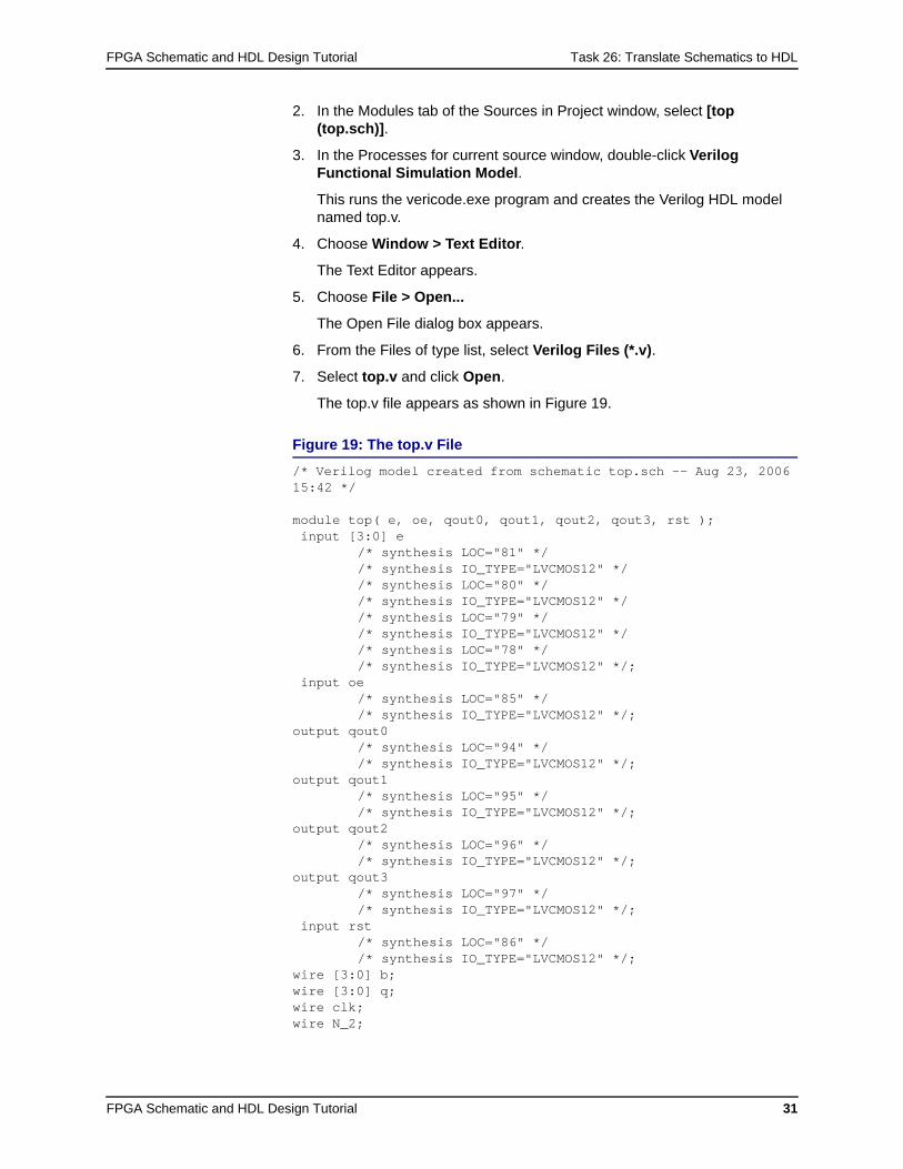
The top.v file appears as shown in Figure 19.
Figure 19: The top.v File
/* Verilog model created from schematic top.sch -- Aug 23, 2006 15:42 */
module top( e, oe, qout0, qout1, qout2, qout3, rst ); input [3:0] e
/* synthesis LOC="81" *//* synthesis IO_TYPE="LVCMOS12" *//* synthesis LOC="80" *//* synthesis IO_TYPE="LVCMOS12" *//* synthesis LOC="79" *//* synthesis IO_TYPE="LVCMOS12" *//* synthesis LOC="78" *//* synthesis IO_TYPE="LVCMOS12" */;
input oe/* synthesis LOC="85" *//* synthesis IO_TYPE="LVCMOS12" */;
output qout0/* synthesis LOC="94" *//* synthesis IO_TYPE="LVCMOS12" */;
output qout1/* synthesis LOC="95" *//* synthesis IO_TYPE="LVCMOS12" */;
output qout2/* synthesis LOC="96" *//* synthesis IO_TYPE="LVCMOS12" */;
output qout3/* synthesis LOC="97" *//* synthesis IO_TYPE="LVCMOS12" */;
input rst/* synthesis LOC="86" *//* synthesis IO_TYPE="LVCMOS12" */;
wire [3:0] b;wire [3:0] q;wire clk;wire N_2;
FPGA Schematic and HDL Design Tutorial Task 27: Implement a Schematic-Based Project
FPGA Schematic and HDL Design Tutorial 32
8. Choose File > Exit.
Task 27: Implement a Schematic-Based ProjectThe quickest way to confirm that the net attributes you defined within a schematic will be correctly applied and are legal is to load the Pre-Map Design Planner to inspect definitions.
To examine schematic net attributes:
1. Select the Project Navigator.
2. In the Sources in Project window, select the target device, LCMXO256C-5T100C.
3. In the Processes for current source window, double-click Design Planner (Pre-Map).
The Design Planner appears.
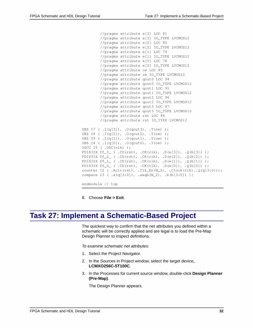
//pragma attribute e[3] LOC 81//pragma attribute e[3] IO_TYPE LVCMOS12//pragma attribute e[2] LOC 80//pragma attribute e[2] IO_TYPE LVCMOS12//pragma attribute e[1] LOC 79//pragma attribute e[1] IO_TYPE LVCMOS12//pragma attribute e[0] LOC 78//pragma attribute e[0] IO_TYPE LVCMOS12//pragma attribute oe LOC 85//pragma attribute oe IO_TYPE LVCMOS12//pragma attribute qout0 LOC 94//pragma attribute qout0 IO_TYPE LVCMOS12//pragma attribute qout1 LOC 95//pragma attribute qout1 IO_TYPE LVCMOS12//pragma attribute qout2 LOC 96//pragma attribute qout2 IO_TYPE LVCMOS12//pragma attribute qout3 LOC 97//pragma attribute qout3 IO_TYPE LVCMOS12//pragma attribute rst LOC 86//pragma attribute rst IO_TYPE LVCMOS12
OBZ I7 ( .I(q[3]), .O(qout3), .T(oe) );OBZ I8 ( .I(q[2]), .O(qout2), .T(oe) );OBZ I9 ( .I(q[1]), .O(qout1), .T(oe) );OBZ I4 ( .I(q[0]), .O(qout0), .T(oe) );OSCC I5 ( .OSC(clk) );FD1S3IX ff_3_ ( .CD(rst), .CK(clk), .D(e[3]), .Q(b[3]) );FD1S3IX ff_2_ ( .CD(rst), .CK(clk), .D(e[2]), .Q(b[2]) );FD1S3IX ff_1_ ( .CD(rst), .CK(clk), .D(e[1]), .Q(b[1]) );FD1S3IX ff_0_ ( .CD(rst), .CK(clk), .D(e[0]), .Q(b[0]) );counter I2 ( .Aclr(rst), .Clk_En(N_2), .Clock(clk),.Q(q[3:0]));compare I3 ( .a(q[3:0]), .aeqb(N_2), .b(b[3:0]) );
endmodule // top
FPGA Schematic and HDL Design Tutorial Summary
FPGA Schematic and HDL Design Tutorial 33
4. In the Design Planner Control window, choose View > Spreadsheet View.
The Spreadsheet View window opens.
5. In Spreadsheet View, select the Port Attributes tab.
Note the Pin and IO_TYPE assignments that have been imported from the schematic.
The Design Planner implements simple error checking to ensure that the user assignments are applicable to the selected device and that there are no conflicting assignments. If the user constraints do not apply to the selected device, or are conflicting with the selected device, the Design Planner displays these constraints in red.
6. From the Design Planner Control window, choose File > Exit.
7. In the Project Navigator’s Processes for current source window, double-click Place & Route Report (4bcount.par).
The .par report is displayed in the Output Panel of the Project Navigator.
SummaryYou have completed the Schematic and HDL Design tutorial. In this tutorial, you have learned how to do the following:
Create a new schematic and select the sheet dimensions.
Create a Verilog HDL template from a block symbol.
Create a schematic symbol from IPexpress.
Create wires, buses, and named nets.
Create an iterated instance of a library symbol.
Edit and modify schematic circuits.
Add net attributes to define sysIO buffer configurations.
Produce output compatible with HDL simulation or synthesis tools.
GlossaryFollowing are the terms and concepts that you should understand to use this tutorial effectively.
HDL. An HDL is a hardware description language, which describes the structure and function of integrated circuits.
netlist. A netlist is an ASCII file describing the logical components in a design and how they are connected. It is basically a list of connectors, a list of instances, and, for each instance, a list of the signals connected to the instance terminals. In addition, the netlist contains attribute information.

FPGA Schematic and HDL Design Tutorial Recommended Reference Materials
FPGA Schematic and HDL Design Tutorial 34
synthesis. Synthesis is the process of translating a high-level design (RTL) description consisting of state machines, truth tables, Boolean equations, or all three into a process-specific gate-level logic implementation.
Verilog. Verilog is a language for describing the structure and function of integrated circuits.
VHDL. VHDL (or VHSIC (Very High-Speed Integrated Circuits) Hardware Description Language) is a language for describing the structure and function of integrated circuits.
Recommended Reference MaterialsThe following reference materials are recommended for this tutorial:
Lattice MachXO Family Data Sheet
ispLEVER FPGA Libraries Help
Lattice sysIO Buffer Usage Guide for the MachXO Family