Embed Size (px)
Citation preview
FPGA ArchitectureFPGA Architecture
Presentation OverviewPresentation Overview Available choice for digital designer FPGA – A detailed look Interconnection Framework
FPGAs and CPLDs Field programmability and programming
technologies SRAM, Anti-fuse, EPROM and EEPROM
Design steps Commercially available devices
Xilinx XC4000 Altera MAX 7000
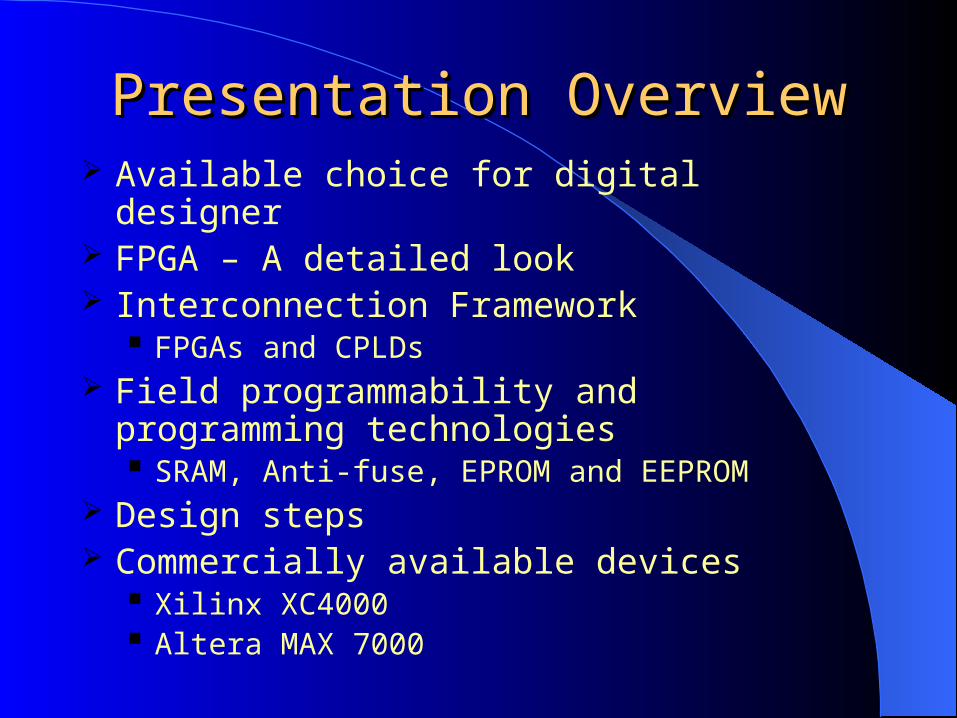
Fixed Versus Programmable LogicFixed Versus Programmable Logic
The circuits in a fixed logic device are permanent, they perform one function or set of functions once manufactured, they cannot be changed.
Programmable logic devices (PLDs) are standard, off-the-shelf parts that offer customers a wide range of logic capacity, features, speed, and voltage characteristics - and these devices can be changed at any time to perform any number of functions.
Classifications
PLA — a Programmable Logic Array (PLA) is a relatively small FPD that contains two levels of logic, an AND- plane and an OR-plane, where both levels are programmable
PAL — a Programmable Array Logic (PAL) is a relatively small FPD that has a programmable AND-plane followed by a fixed OR-plane
SPLD — refers to any type of Simple PLD, usually either a PLA or PAL
CPLD — a more Complex PLD that consists of an arrangement of multiple SPLD-like blocks on a single chip.
FPGA — a Field-Programmable Gate Array is an FPD featuring a general structure that allows very high logic capacity.
Definitions
Field Programmable Device (FPD):
— a general term that refers to any type of integrated
circuit used for implementing digital hardware, where the
chip can be configured by the end user to realize
different designs.
—Programming of such a device often involves placing
the chip into a special programming unit, but some chips
can also be configured “in-system”. Another name for
FPDs is programmable logic devices (PLDs).
Designer’s ChoiceDesigner’s Choice Digital designer has various options
SSI (small scale integrated circuits) or MSI (medium scale integrated circuits) components
Difficulties arises as design size increases Interconnections grow with complexity resulting in a
prolonged testing phase
Simple programmable logic devices PALs (programmable array logic) PLAs (programmable logic array)
Architecture not scalable; Power consumption and delays play an important role in extending the architecture to complex designs
Implementation of larger designs leads to same difficulty as that of discrete components
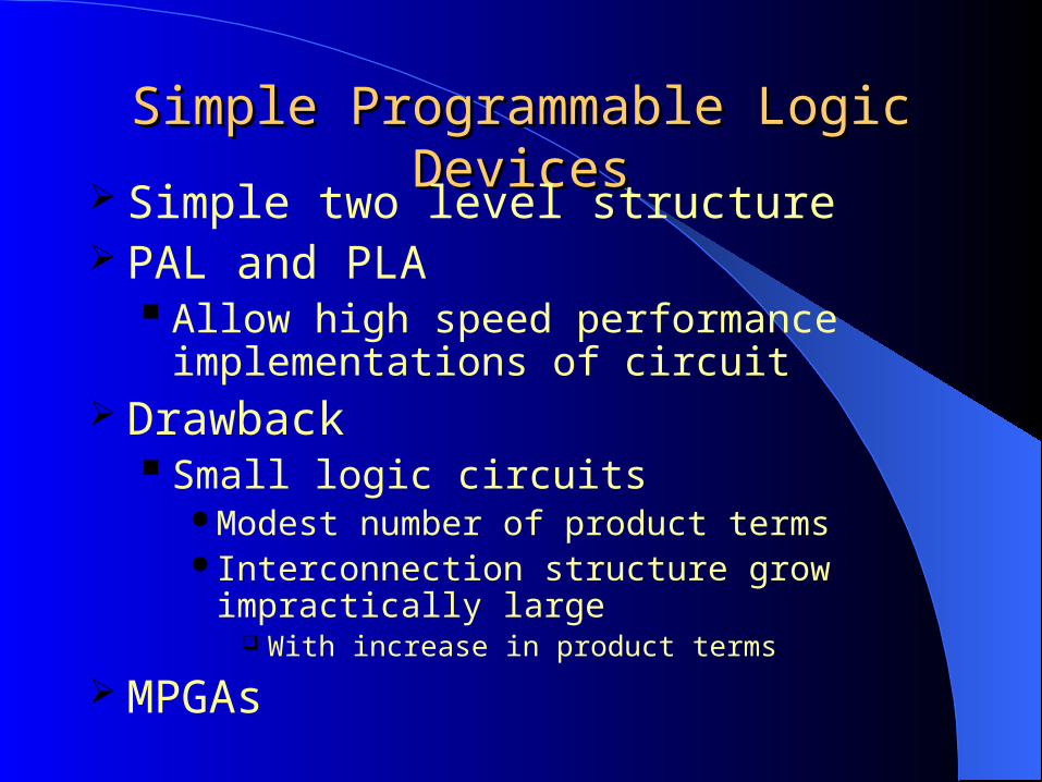
Simple Programmable Logic DevicesSimple Programmable Logic Devices Simple two level structure PAL and PLA
Allow high speed performance implementations of circuit
Drawback Small logic circuits
Modest number of product termsInterconnection structure grow impractically
large With increase in product terms
MPGAs
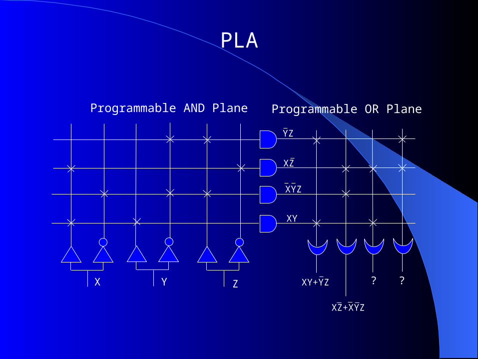
PLA
Programmable AND Plane Programmable OR Plane
X Y Z XY+YZ ? ?
XZ+XYZ
YZ
XZ
XYZ
XY
PLA
Programmable AND Plane
X Y O1 O2 O3 O4
Programmable Node
Programmable OR Plane
Connect
Disconnect
X X Y Y
XY
XY XY
XYXY
Un-programmed
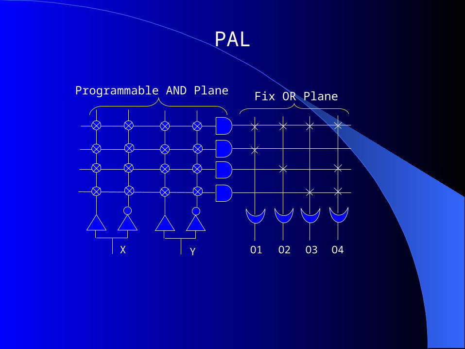
PAL
Programmable AND Plane
X Y O1 O2 O3 O4
Fix OR Plane
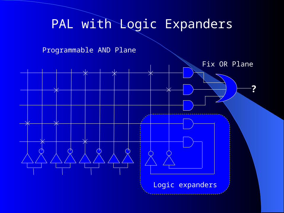
PAL with Logic Expanders
Programmable AND Plane
Logic expanders
Fix OR Plane
?
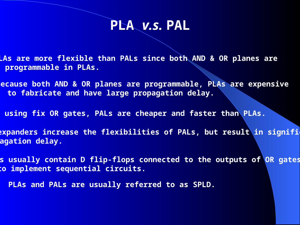
PLA v.s. PAL
PLAs are more flexible than PALs since both AND & OR planes are programmable in PLAs.
Because both AND & OR planes are programmable, PLAs are expensive to fabricate and have large propagation delay.
By using fix OR gates, PALs are cheaper and faster than PLAs.
Logic expanders increase the flexibilities of PALs, but result in significant propagation delay.
PALs usually contain D flip-flops connected to the outputs of OR gates to implement sequential circuits.
PLAs and PALs are usually referred to as SPLD.
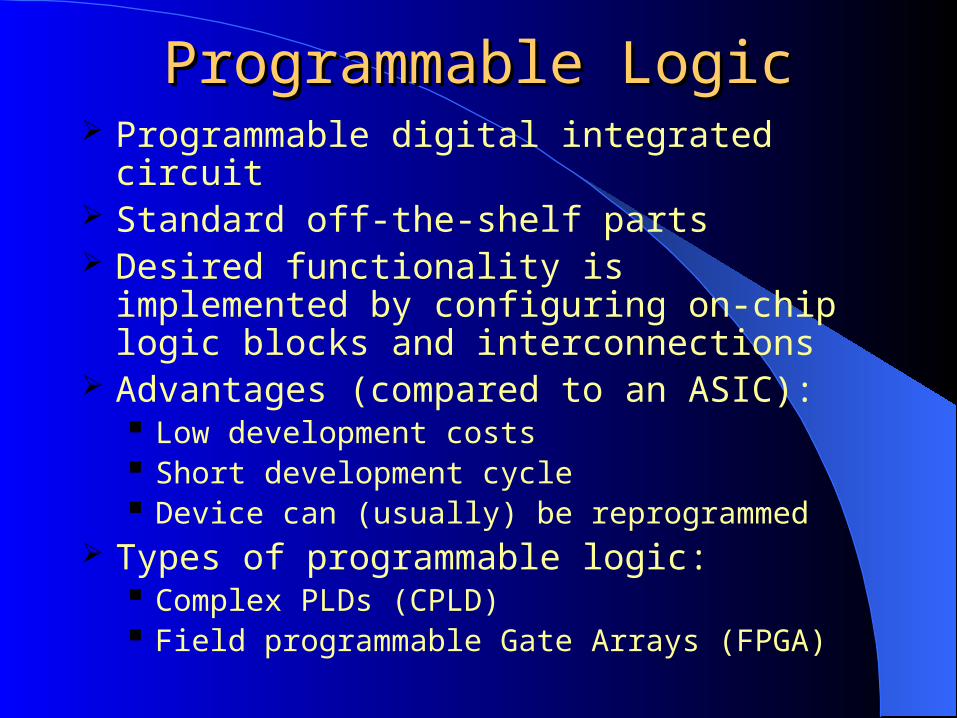
Programmable LogicProgrammable Logic Programmable digital integrated circuit Standard off-the-shelf parts Desired functionality is implemented by
configuring on-chip logic blocks and interconnections
Advantages (compared to an ASIC): Low development costs Short development cycle Device can (usually) be reprogrammed
Types of programmable logic: Complex PLDs (CPLD) Field programmable Gate Arrays (FPGA)
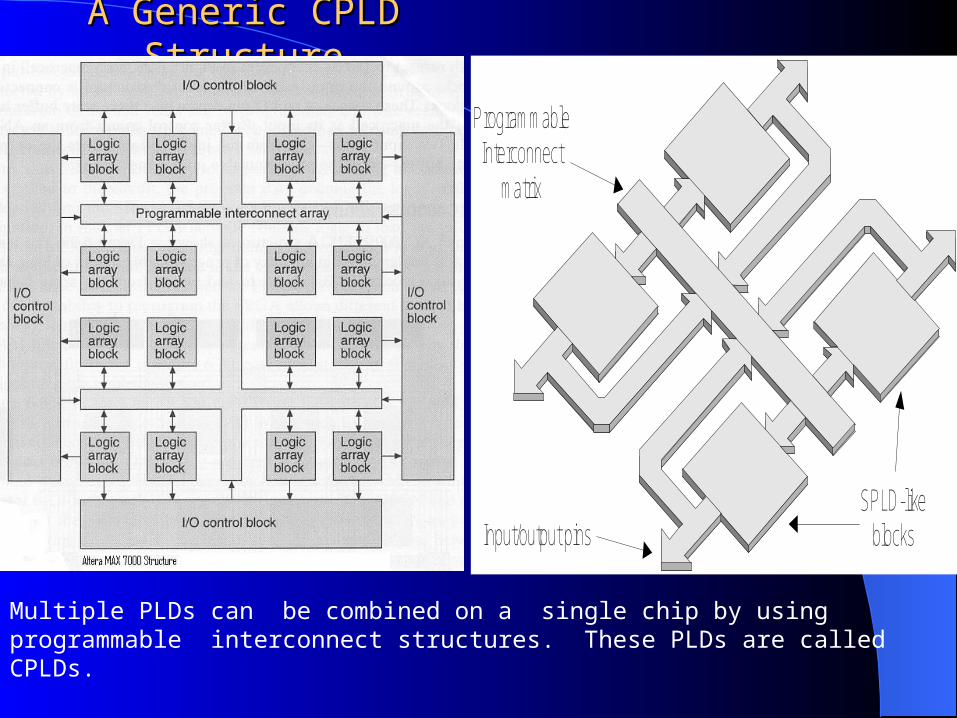
A Generic CPLD StructureA Generic CPLD Structure
ProgrammableInterconnect
matrix
Input/output pinsSPLD-like
blocks
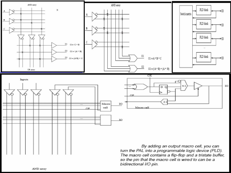
Multiple PLDs can be combined on a single chip by using programmable interconnect structures. These PLDs are called CPLDs.
CPLDCPLDArchitecture and ExamplesArchitecture and Examples
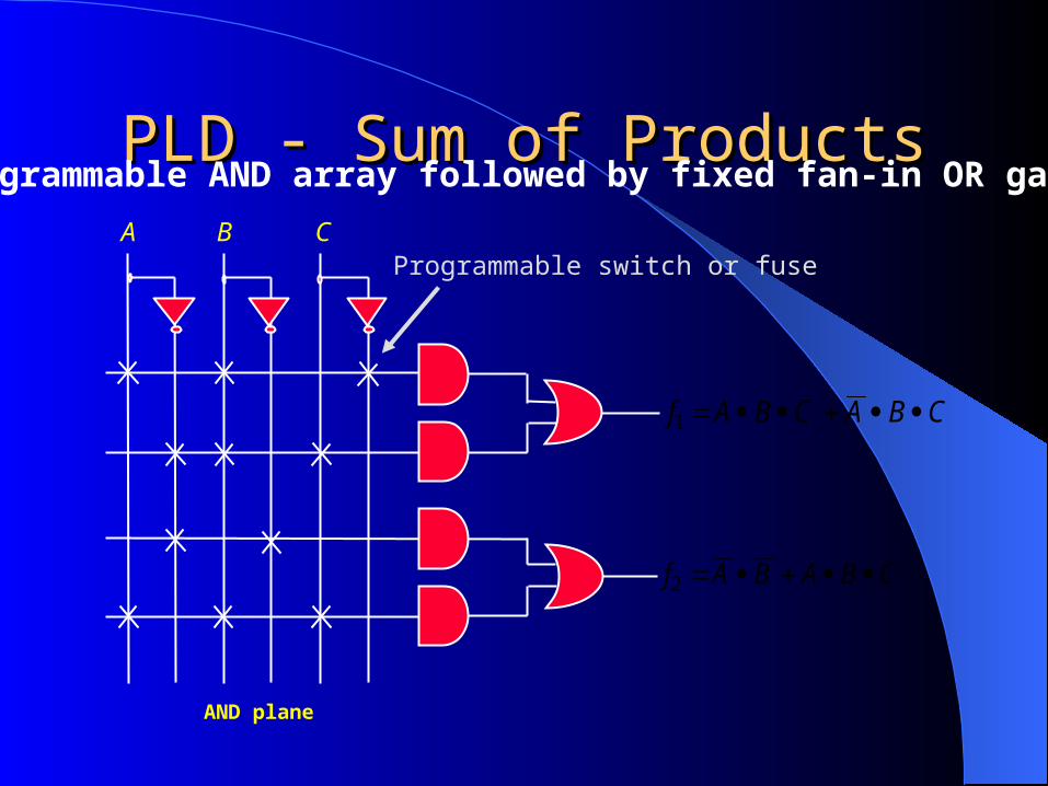
PLD - Sum of ProductsPLD - Sum of ProductsA B C
CBACBAf 1
CBABAf 2
AND plane
Programmable AND array followed by fixed fan-in OR gates
Programmable switch or fuse
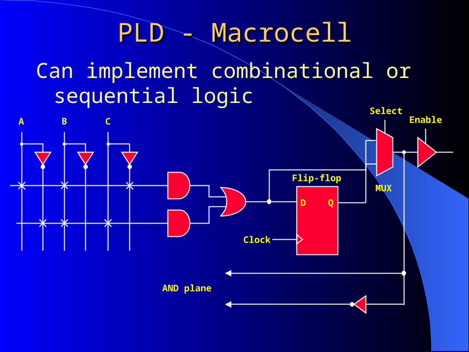
PLD - MacrocellPLD - MacrocellCan implement combinational or
sequential logic A B C
Flip-flop
SelectEnable
D Q
Clock
AND plane
MUX
1f
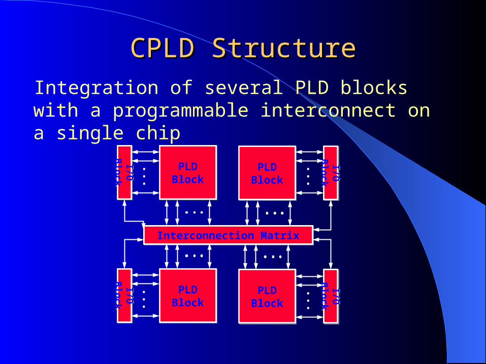
CPLD StructureCPLD StructureIntegration of several PLD blocks with a programmable interconnect on a single chip
PLDBlockPLD
BlockPLD
BlockPLD
Block
Interconnection MatrixInterconnection Matrix
I/O B
lock
I/O B
lock
I/O B
lock
I/O B
lock
PLDBlockPLD
BlockPLD
BlockPLD
Block
I/O B
lock
I/O B
lock
I/O B
lock
I/O B
lock
• • •
Interconnection MatrixInterconnection Matrix
• • •
• • •
• • •
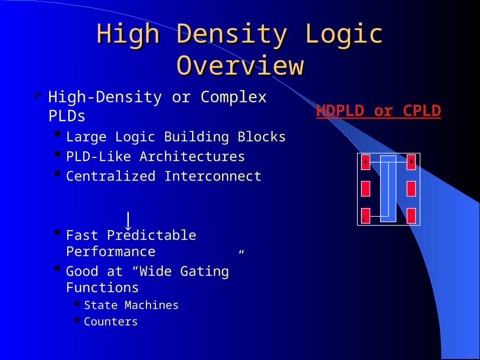
High Density Logic OverviewHigh Density Logic Overview
High-Density or Complex PLDs Large Logic Building Blocks PLD-Like Architectures Centralized Interconnect
Fast Predictable Performance Good at “Wide Gating”
Functions State Machines Counters
A B
C
HDPLD or CPLD
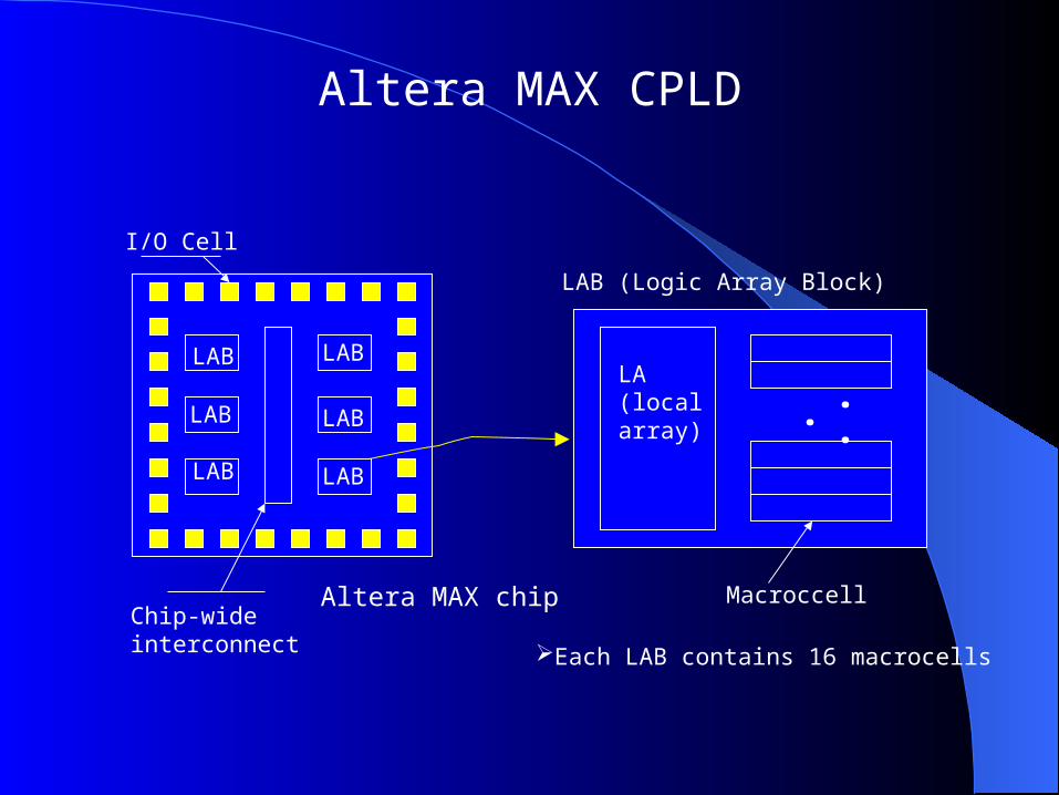
Altera MAX CPLD
LAB
LAB
LABLAB
LAB
LAB
I/O Cell
Chip-wideinterconnect
Altera MAX chip
LAB (Logic Array Block)
LA(local array) •
• •
Macroccell
Each LAB contains 16 macrocells
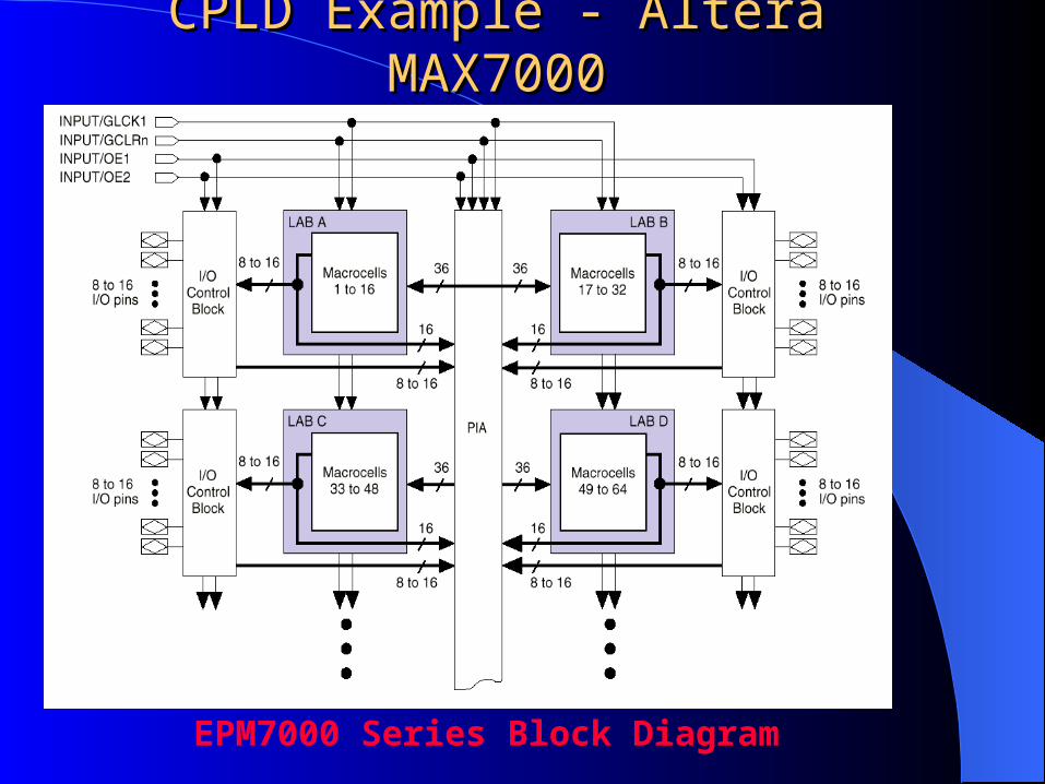
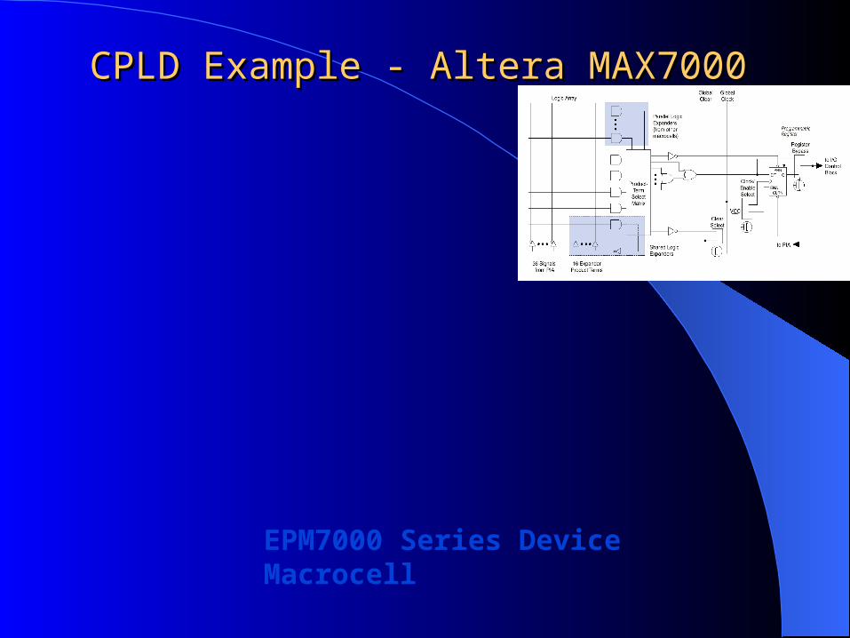
CPLD Example - Altera MAX7000CPLD Example - Altera MAX7000
EPM7000 Series Block Diagram
CPLD Example - Altera MAX7000CPLD Example - Altera MAX7000
MAX 7000 architecture includes Logic array blocks Macrocells Expander product terms( shareable and parallel) Programmable interconnect array I/O control blocks
Performance Linking high performance and flexible LABs
Programmable interconnect array (PIA) Global bus fed by all dedicated inputs I/O pins Macrocells
Configured Combinational or Sequential logic operations
CPLD Example - Altera MAX7000CPLD Example - Altera MAX7000
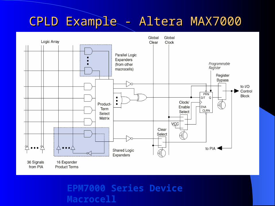
EPM7000 Series Device Macrocell
CPLD Example - Altera MAX7000CPLD Example - Altera MAX7000
Macrocell Logic array
Combinational logic is implemented in the array Five products terms
Product-term select matrix Allocate product terms
Primary logic inputs to AND or XOR gates– Combinational logic
Secondary inputs to the register – Clear, preset, clock, clock enable control functions
Programmable register Logic expanders
Each LAB has16 Shareable expanders Inverted product terms fed back into the logic array
Parallel expanders Product terms borrowed from adjacent macrocells
CPLD Example - Altera MAX7000CPLD Example - Altera MAX7000
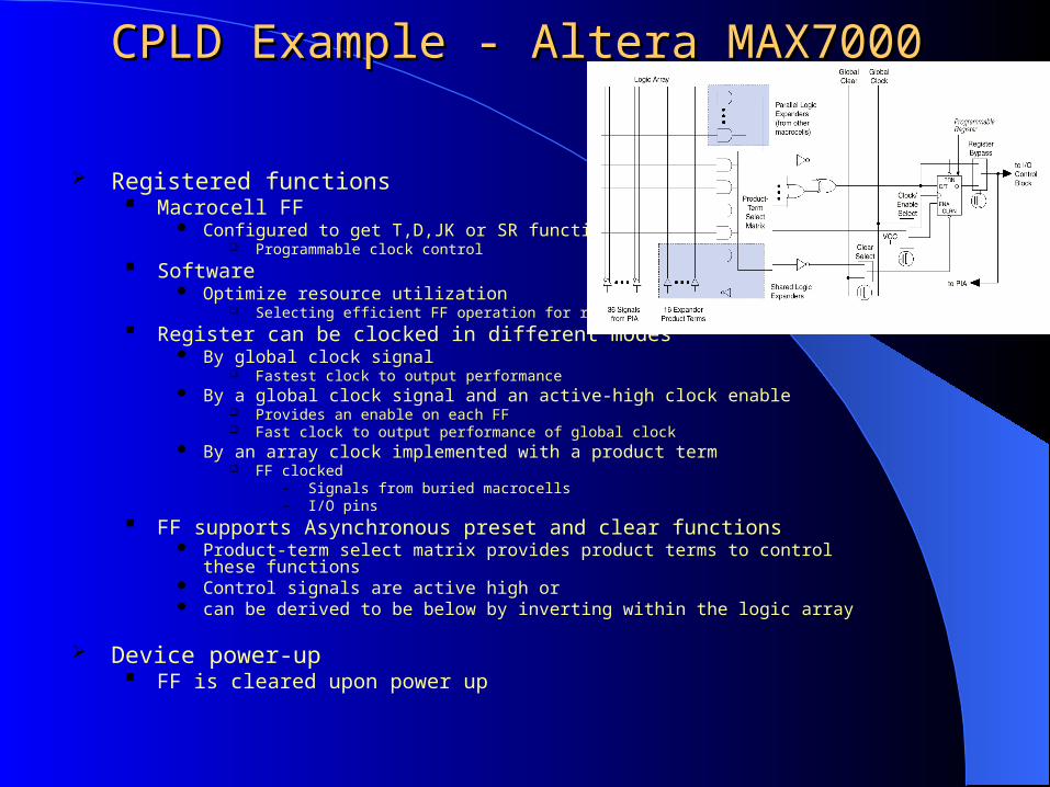
Registered functions Macrocell FF
Configured to get T,D,JK or SR functions Programmable clock control
Software Optimize resource utilization
Selecting efficient FF operation for registered function
Register can be clocked in different modes By global clock signal
Fastest clock to output performance By a global clock signal and an active-high clock enable
Provides an enable on each FF Fast clock to output performance of global clock
By an array clock implemented with a product term FF clocked
– Signals from buried macrocells– I/O pins
FF supports Asynchronous preset and clear functions Product-term select matrix provides product terms to control these functions Control signals are active high or can be derived to be below by inverting within the logic array
Device power-up FF is cleared upon power up
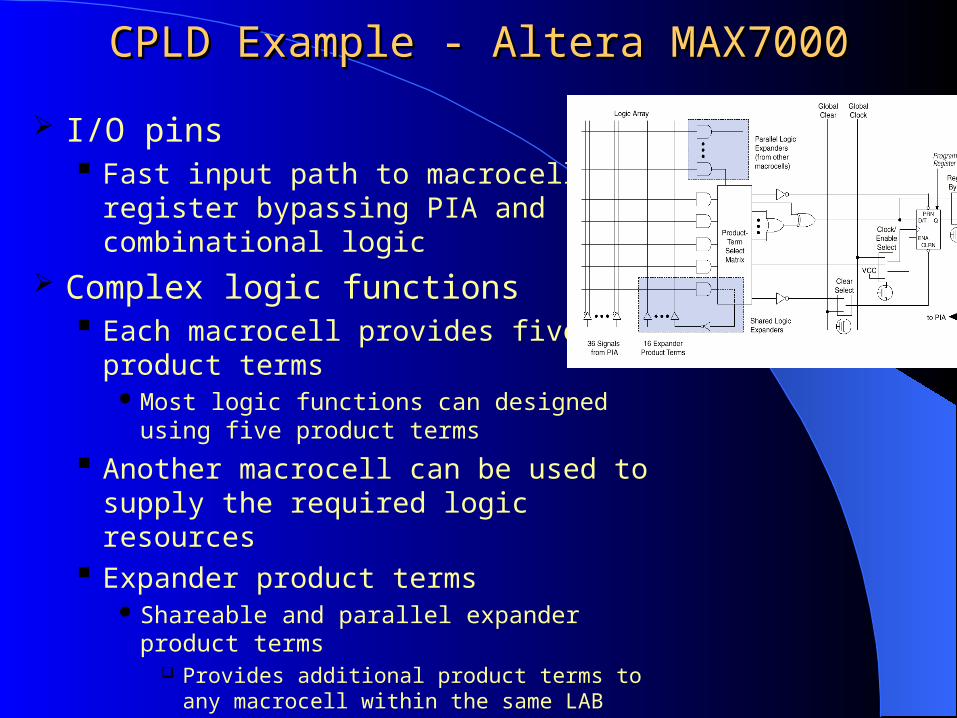
CPLD Example - Altera MAX7000CPLD Example - Altera MAX7000
I/O pins Fast input path to macrocell register
bypassing PIA and combinational logic
Complex logic functions Each macrocell provides five product
terms Most logic functions can designed using five
product terms
Another macrocell can be used to supply the required logic resources
Expander product terms Shareable and parallel expander product
terms Provides additional product terms to any
macrocell within the same LAB
CPLD Example - Altera MAX7000CPLD Example - Altera MAX7000
EPM7000 Series Device Macrocell
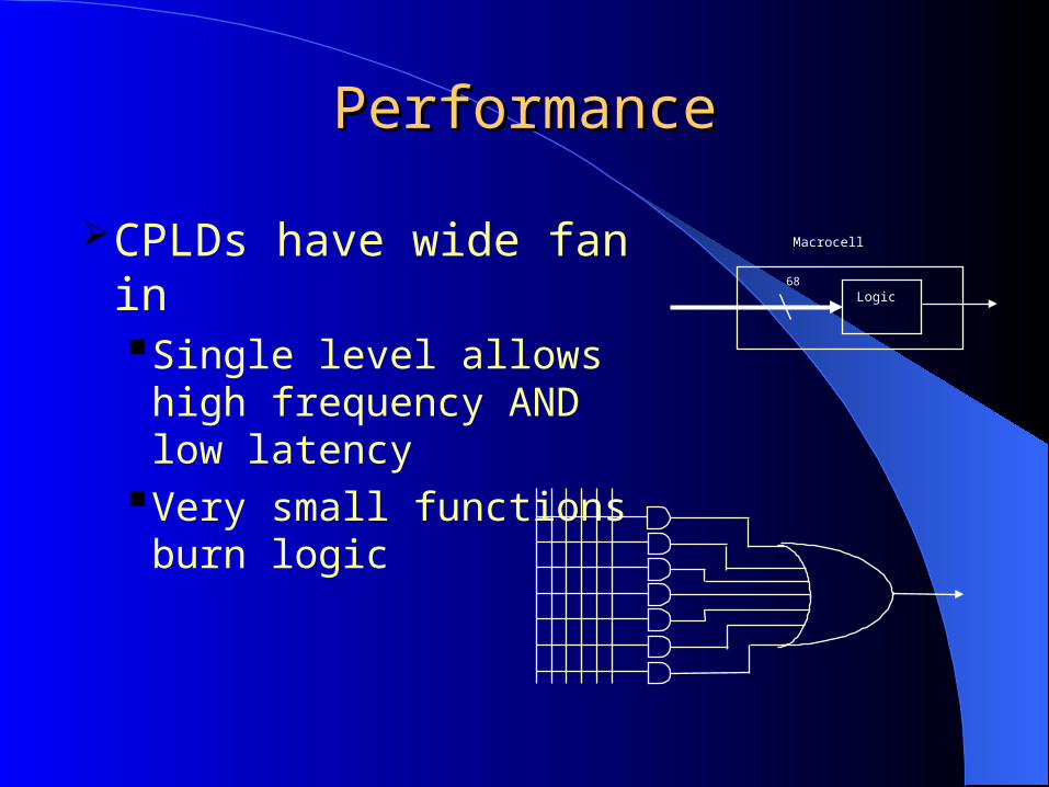
PerformancePerformance
CPLDs have wide fan in Single level allows high
frequency AND low latency
Very small functions burn logic
Logic68
Macrocell
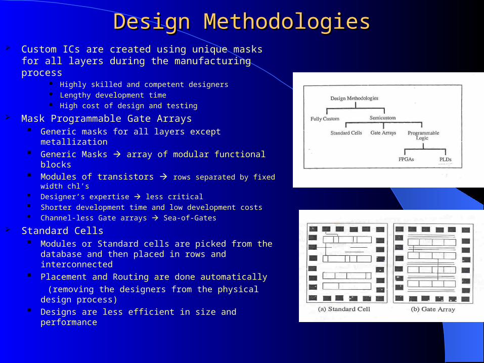
Design MethodologiesDesign Methodologies Custom ICs are created using unique masks for all
layers during the manufacturing process Highly skilled and competent designers Lengthy development time High cost of design and testing
Mask Programmable Gate Arrays Generic masks for all layers except metallization Generic Masks array of modular functional blocks Modules of transistors rows separated by fixed width chl’s Designer’s expertise less critical Shorter development time and low development costs Channel-less Gate arrays Sea-of-Gates
Standard Cells Modules or Standard cells are picked from the database
and then placed in rows and interconnected Placement and Routing are done automatically
(removing the designers from the physical design process) Designs are less efficient in size and performance
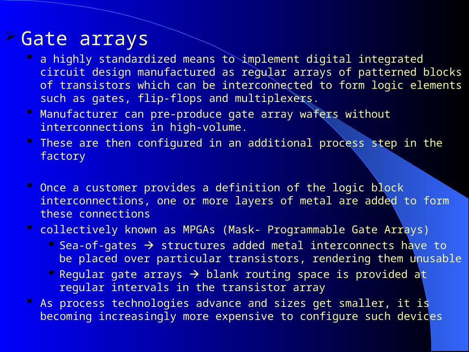
Gate arrays a highly standardized means to implement digital integrated circuit design
manufactured as regular arrays of patterned blocks of transistors which can be interconnected to form logic elements such as gates, flip-flops and multiplexers.
Manufacturer can pre-produce gate array wafers without interconnections in high-volume.
These are then configured in an additional process step in the factory
Once a customer provides a definition of the logic block interconnections, one or more layers of metal are added to form these connections
collectively known as MPGAs (Mask- Programmable Gate Arrays) Sea-of-gates structures added metal interconnects have to be placed over
particular transistors, rendering them unusable Regular gate arrays blank routing space is provided at regular intervals in
the transistor array As process technologies advance and sizes get smaller, it is becoming
increasingly more expensive to configure such devices
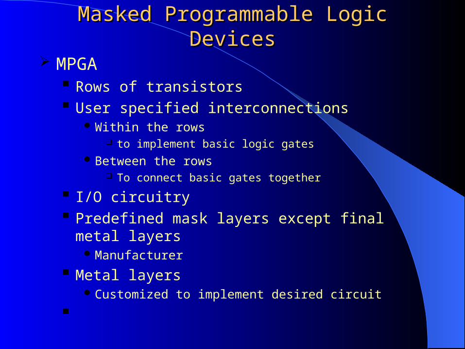
Masked Programmable Logic DevicesMasked Programmable Logic Devices
MPGA Rows of transistors User specified interconnections
Within the rows to implement basic logic gates
Between the rows To connect basic gates together
I/O circuitry Predefined mask layers except final metal layers
Manufacturer
Metal layers Customized to implement desired circuit
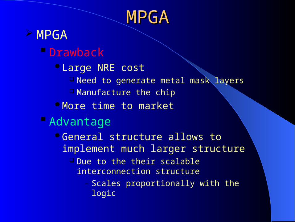
MPGAMPGA MPGA
DrawbackLarge NRE cost
Need to generate metal mask layers Manufacture the chip
More time to market
AdvantageGeneral structure allows to implement much
larger structure Due to the their scalable interconnection structure
– Scales proportionally with the logic
Field Programmable Logic DevicesField Programmable Logic Devices
FPGAs Programmability of PLD Scalable interconnection structure of an
MPGA
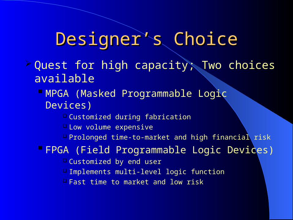
Designer’s ChoiceDesigner’s Choice Quest for high capacity; Two choices
available MPGA (Masked Programmable Logic
Devices) Customized during fabrication Low volume expensive Prolonged time-to-market and high financial risk
FPGA (Field Programmable Logic Devices) Customized by end user Implements multi-level logic function Fast time to market and low risk
Designer’s ChoiceDesigner’s Choice
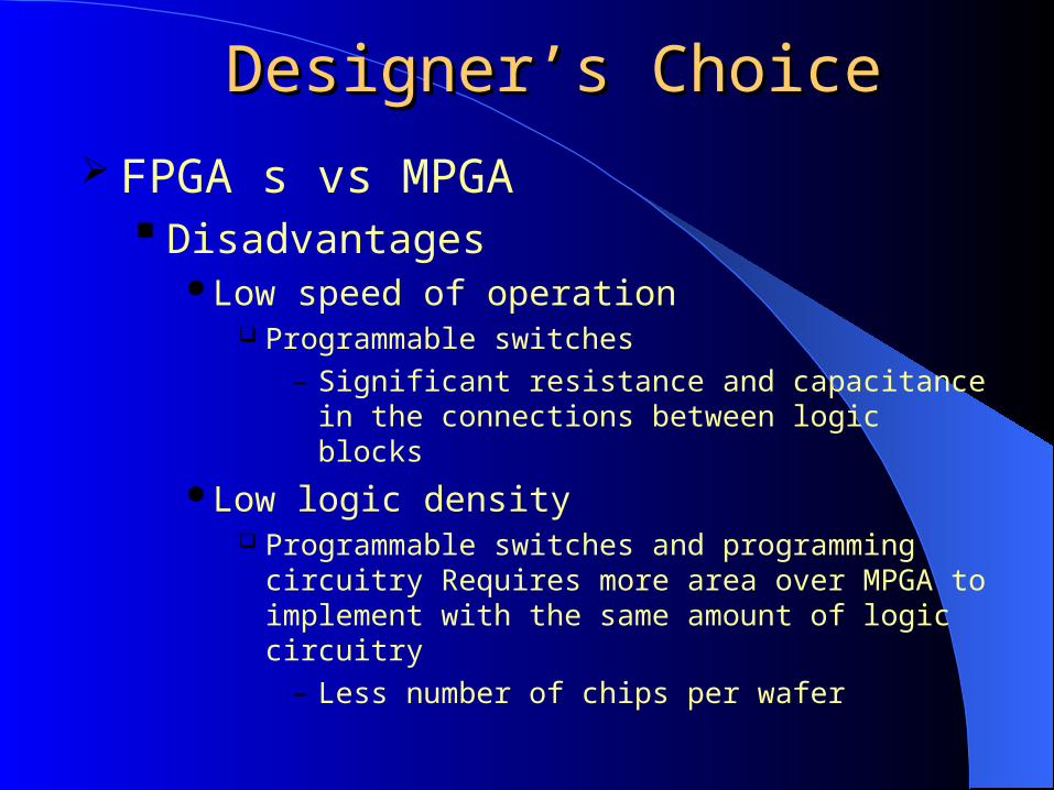
FPGA s vs MPGA Disadvantages
Low speed of operation Programmable switches
– Significant resistance and capacitance in the connections between logic blocks
Low logic density Programmable switches and programming circuitry
Requires more area over MPGA to implement with the same amount of logic circuitry
– Less number of chips per wafer
FPGA s vs MPGAFPGA s vs MPGA
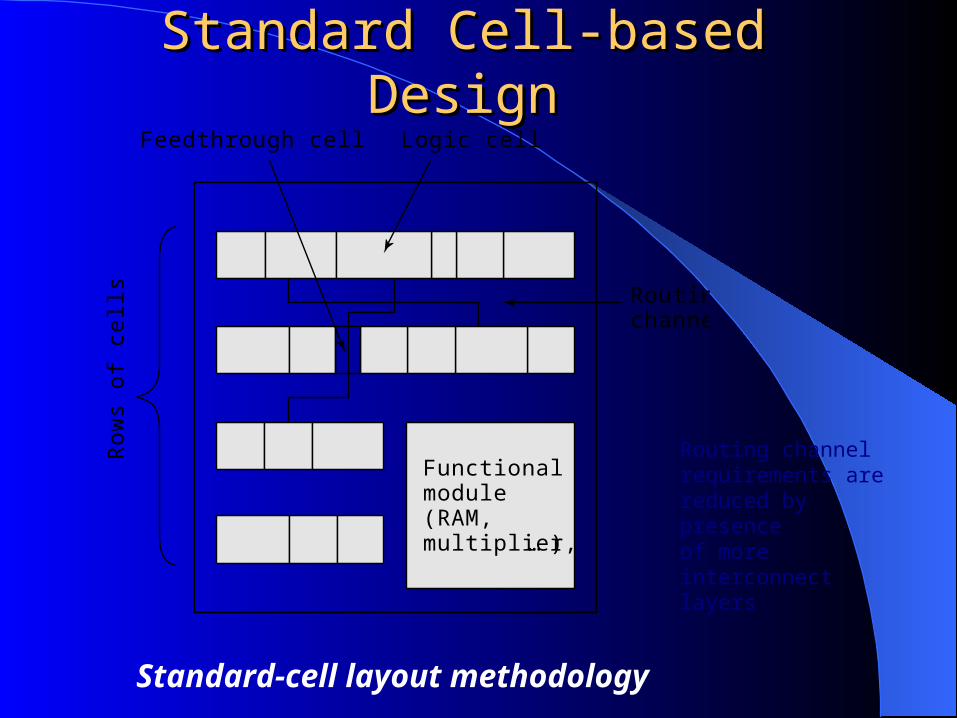
Standard Cell-based DesignStandard Cell-based Design
Routing channel requirements arereduced by presenceof more interconnectlayers
Functionalmodule(RAM,multiplier,…)
Routingchannel
Logic cellFeedthrough cellR
ow
s o
f ce
lls
Standard-cell layout methodology
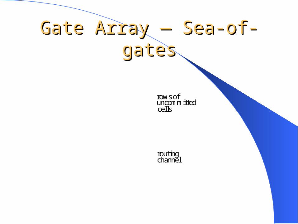
Gate Array — Sea-of-gatesGate Array — Sea-of-gates
rows of
cells
routing channel
uncommitted
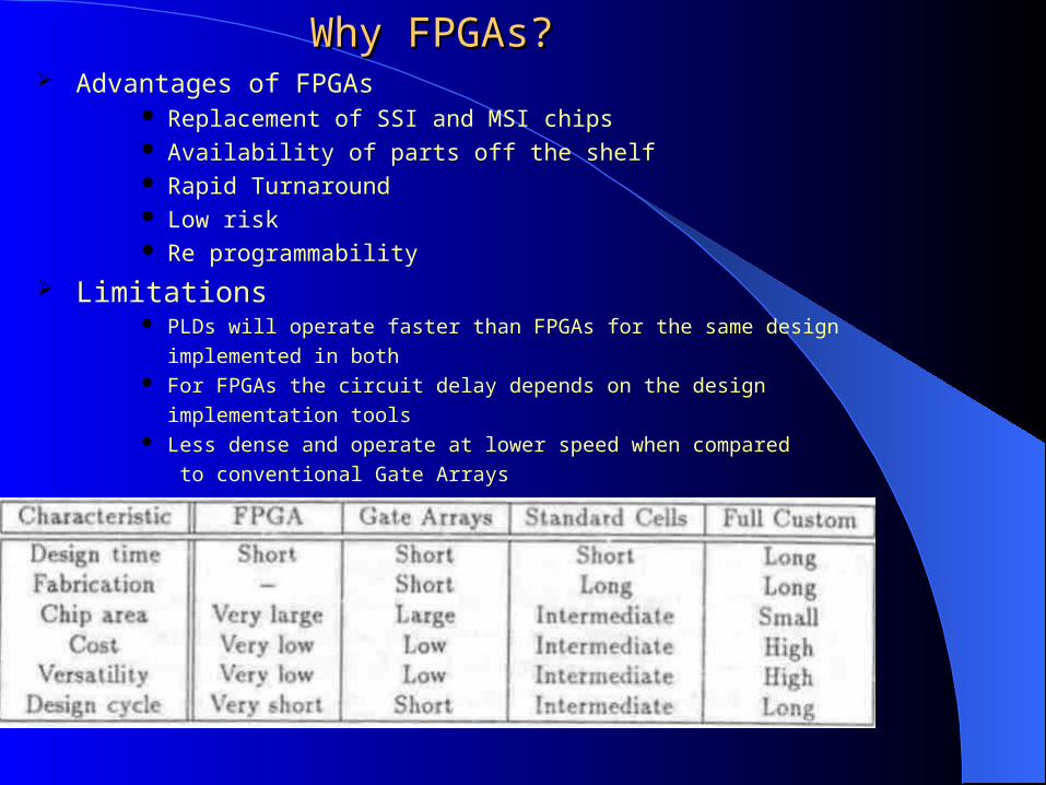
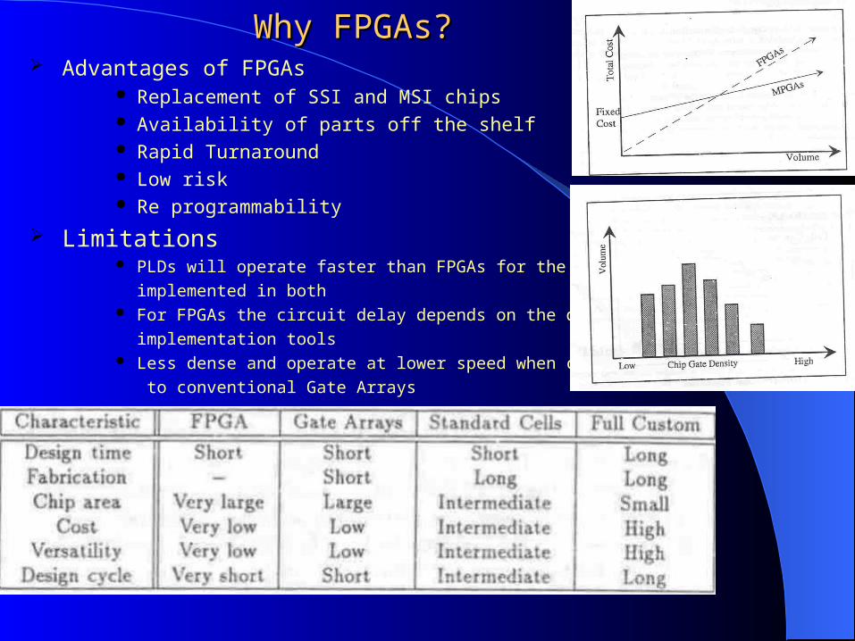
Why FPGAs?Why FPGAs? Advantages of FPGAs
Replacement of SSI and MSI chips Availability of parts off the shelf Rapid Turnaround Low risk Re programmability
Limitations PLDs will operate faster than FPGAs for the same design
implemented in both For FPGAs the circuit delay depends on the design
implementation tools Less dense and operate at lower speed when compared
to conventional Gate Arrays
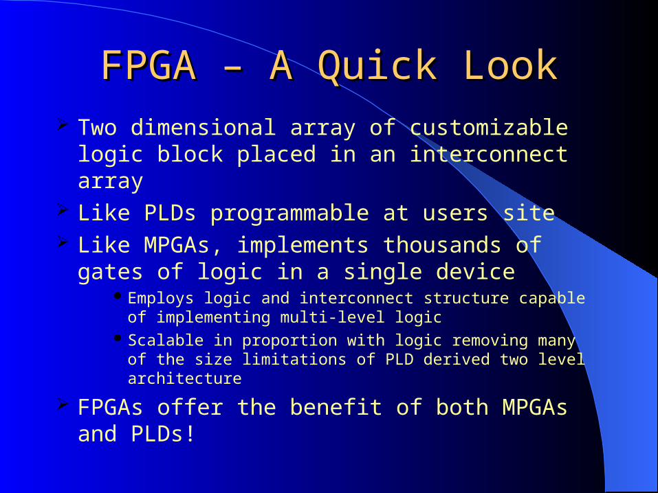
FPGA – A Quick LookFPGA – A Quick Look Two dimensional array of customizable logic
block placed in an interconnect array Like PLDs programmable at users site Like MPGAs, implements thousands of gates
of logic in a single device Employs logic and interconnect structure capable of
implementing multi-level logic Scalable in proportion with logic removing many of the
size limitations of PLD derived two level architecture
FPGAs offer the benefit of both MPGAs and PLDs!
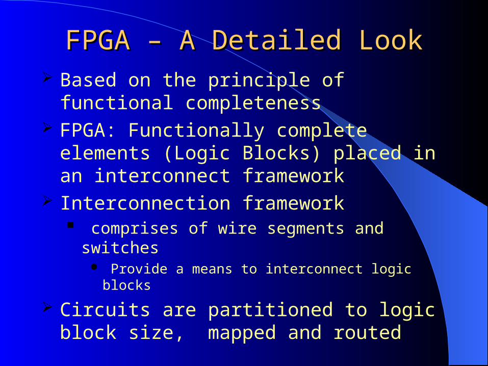
FPGA – A Detailed LookFPGA – A Detailed Look Based on the principle of functional
completeness FPGA: Functionally complete elements
(Logic Blocks) placed in an interconnect framework
Interconnection framework comprises of wire segments and switches
Provide a means to interconnect logic blocks
Circuits are partitioned to logic block size, mapped and routed
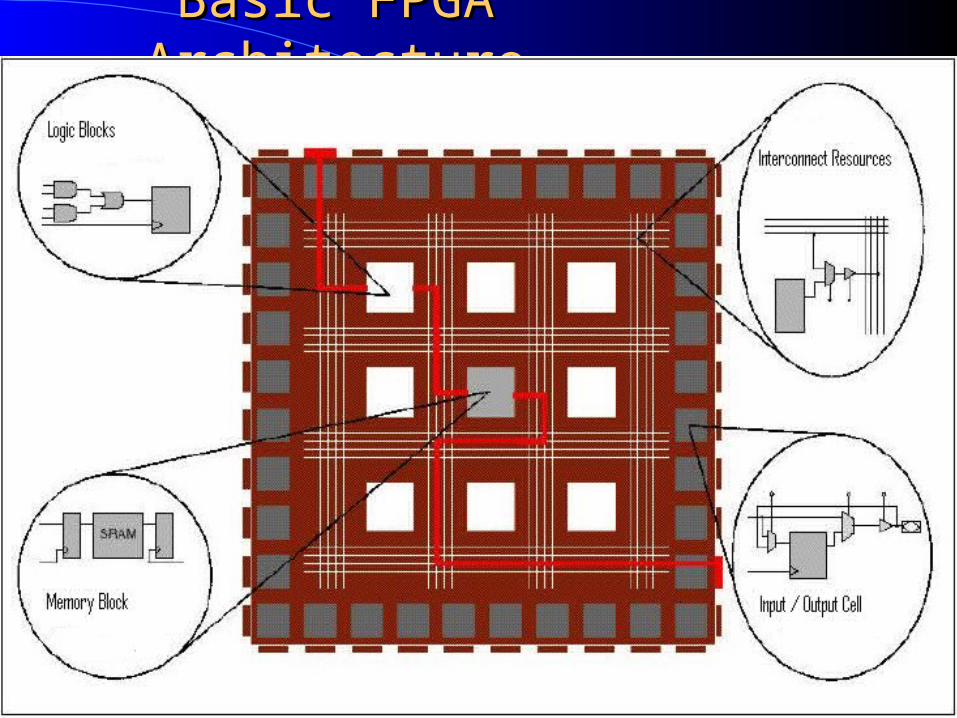
Basic FPGA ArchitectureBasic FPGA Architecture
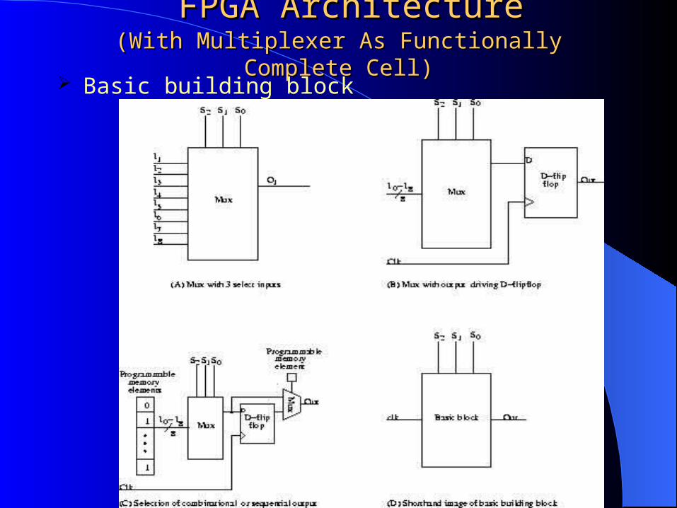
FPGA ArchitectureFPGA Architecture(With Multiplexer As Functionally Complete Cell)(With Multiplexer As Functionally Complete Cell)
Basic building block
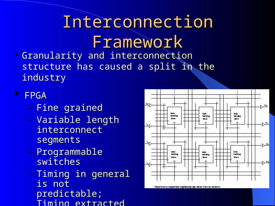
Interconnection FrameworkInterconnection Framework Granularity and interconnection structure has
caused a split in the industry
FPGA– Fine grained– Variable length
interconnect segments– Programmable switches– Timing in general is not
predictable; Timing extracted after placement and route
Interconnection FrameworkInterconnection Framework
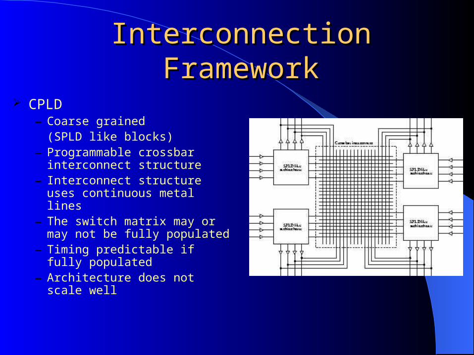
CPLD– Coarse grained
(SPLD like blocks)– Programmable crossbar
interconnect structure– Interconnect structure uses
continuous metal lines– The switch matrix may or may
not be fully populated– Timing predictable if fully
populated– Architecture does not scale well
Field ProgrammabilityField Programmability
Field programmability is achieved through switches (Transistors controlled by memory elements or fuses)
Switches control the following aspects Interconnection among wire segments Configuration of logic blocks
Distributed memory elements controlling the switches and configuration of logic blocks are together called “Configuration Memory”
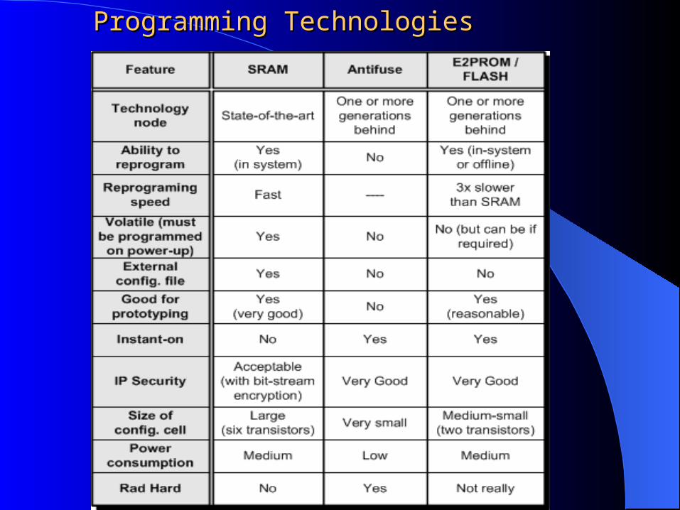
Technology of Programmable Technology of Programmable ElementsElements
Vary from vendor to vendor. All share the common property: Configurable in one of the two positions – ‘ON’ or ‘OFF’
Can be classified into three categories: SRAM based Fuse based EPROM/EEPROM/Flash based
Desired properties: Minimum area consumption Low on resistance; High off resistance Low parasitic capacitance to the attached wire Reliability in volume production
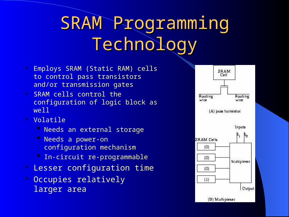
SRAM Programming SRAM Programming TechnologyTechnology
Employs SRAM (Static RAM) cells to control pass transistors and/or transmission gates
SRAM cells control the configuration of logic block as well
Volatile Needs an external storage Needs a power-on configuration
mechanism In-circuit re-programmable
Lesser configuration time Occupies relatively larger
area
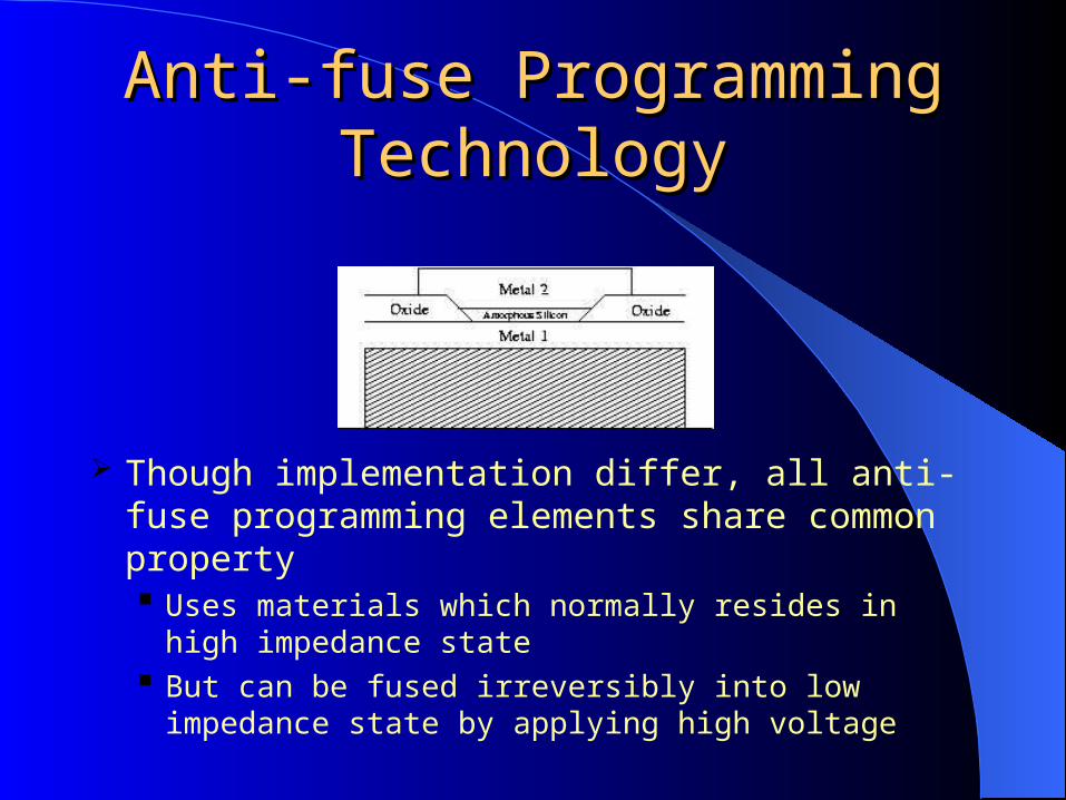
Anti-fuse Programming Anti-fuse Programming TechnologyTechnology
Though implementation differ, all anti-fuse programming elements share common property Uses materials which normally resides in high
impedance state But can be fused irreversibly into low impedance state
by applying high voltage
Anti-fuse Programming Anti-fuse Programming TechnologyTechnology
Very low ON Resistance (Faster implementation of circuits)
Limited size of anti-fuse elements; Interconnects occupy relatively lesser area Offset : Larger transistors needed for
programming
One Time Programmable Cannot be re-programmed
(Design changes are not possible)
Retain configuration after power off
EPROM, EEPROM or Flash EPROM, EEPROM or Flash Based Programming TechnologyBased Programming Technology
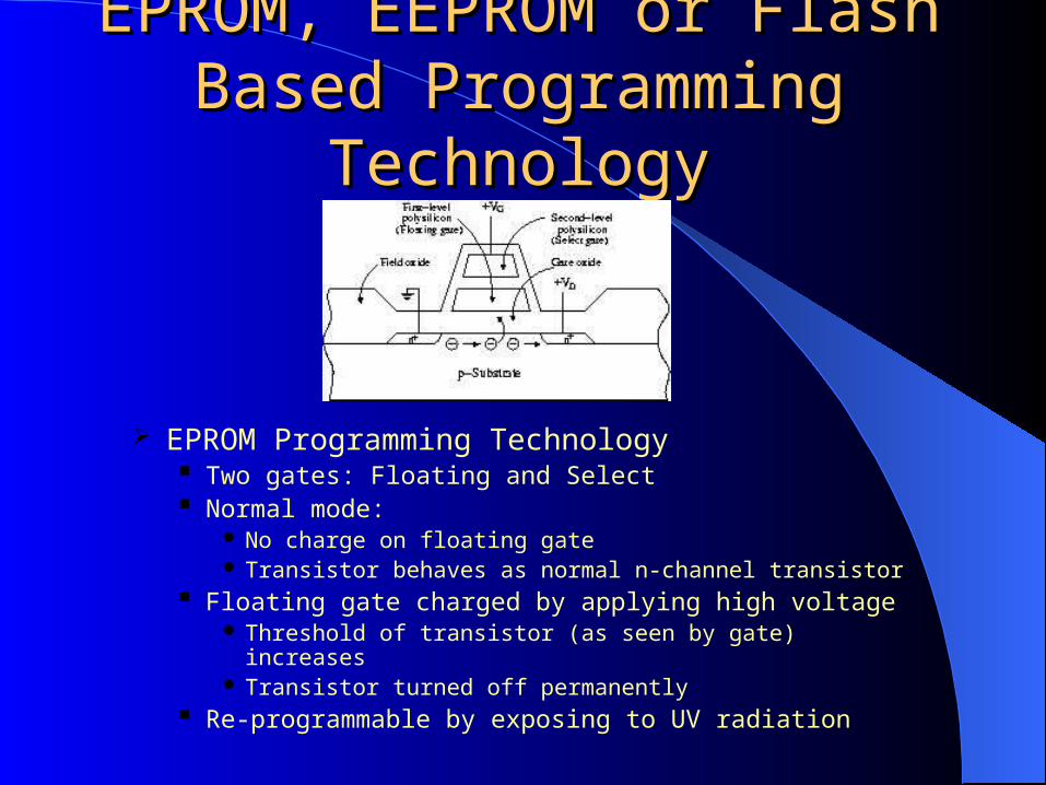
EPROM Programming Technology Two gates: Floating and Select Normal mode:
No charge on floating gate Transistor behaves as normal n-channel transistor
Floating gate charged by applying high voltage Threshold of transistor (as seen by gate) increases Transistor turned off permanently
Re-programmable by exposing to UV radiation
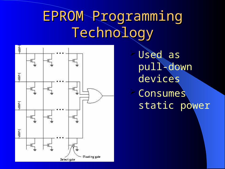
EPROM Programming EPROM Programming TechnologyTechnology
Used as pull-down devices
Consumes static power
EPROM Programming EPROM Programming TechnologyTechnology
No external storage mechanism Re-programmable (Not all!) Not in-system re-programmable Re-programming is a time consuming
task
EEPROM Programming EEPROM Programming TechnologyTechnology
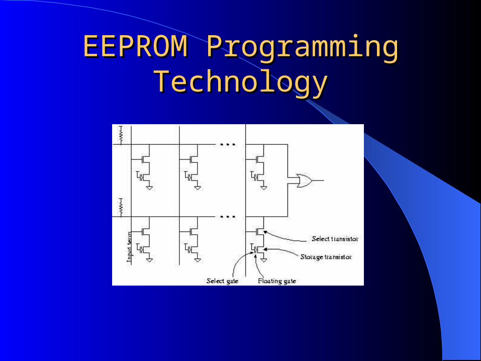
Two gates: Floating and Select Functionally equivalent to EPROM;
Construction and structure differ Electrically Erasable: Re-programmable by
applying high voltage
(No UV radiation expose!) When un-programmed, the threshold (as
seen by select gate) is negative!
EEPROM Programming EEPROM Programming TechnologyTechnology
EEPROM Programming EEPROM Programming TechnologyTechnology
Re-programmable; In general, in-system re-programmable
Re-programming consumes lesser time compared to EPROM technology
Multiple voltage sources may be required
Area occupied is twice that of EPROM!
Programming TechnologiesProgramming Technologies
Basic architectures of FPGAs
An FPGA device to allow the implementation of practically any logic circuit requires an area trade-off between a sufficient number of
flexible configurable logical cells and enough interconnect resources to allow all connections between these cells.
majority of circuits a small portion of routing and logic resources, Resulting in a loss in speed (signal passing through redundant routing
elements) density of logic when compared to the same circuit implemented in dedicated
logic. grouping of different FPGA devices with related architecture into a
family. Each member in a family would be physically tailored to a certain class of
application architecture, by for example replacing the switches in certain routes by hard shorts, or hard-wiring the logical cells internally in a certain manner.
This member may now implement certain circuits more efficiently, but its reduced flexibility means that some circuits may not fit at all onto the device.
Implementation of a circuit is now a question of choosing the right device from the FPGA family.

Programming Skills vs. FPGAsProgramming Skills vs. FPGAs
Single-threadingNo synchronizationfor/if/switch control
Incremental executionOne instruction at a timeResults are immediate
Common parallelizationLarge units of workCostly communication
Massive parallelismVisible timing relationsState machine/hardwired
Pipelined executionAll operations activeVisible dependencies
Parallelism modelFine grain – one ALU opCheap on-chip comm.
CPU Model FPGA Model
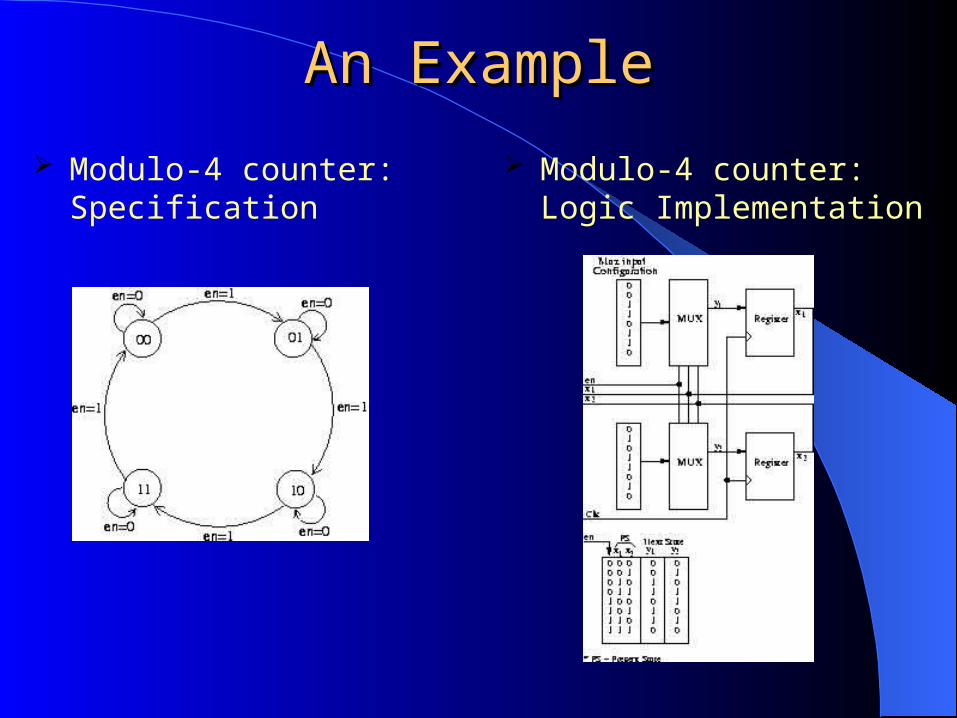
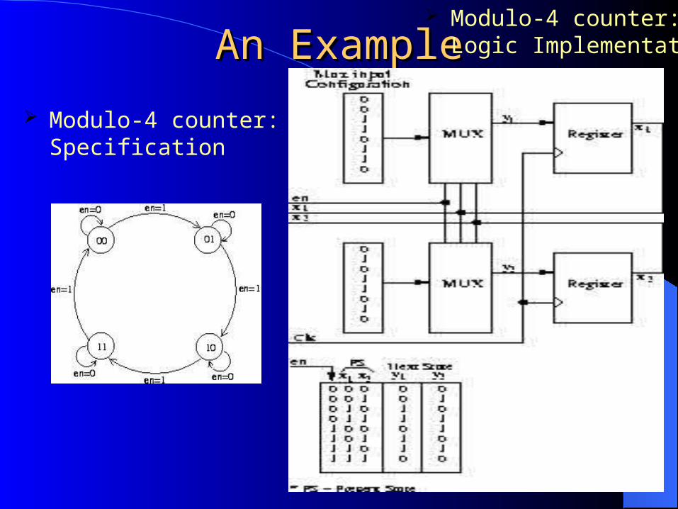
An ExampleAn Example
Modulo-4 counter: Specification
Modulo-4 counter: Logic Implementation
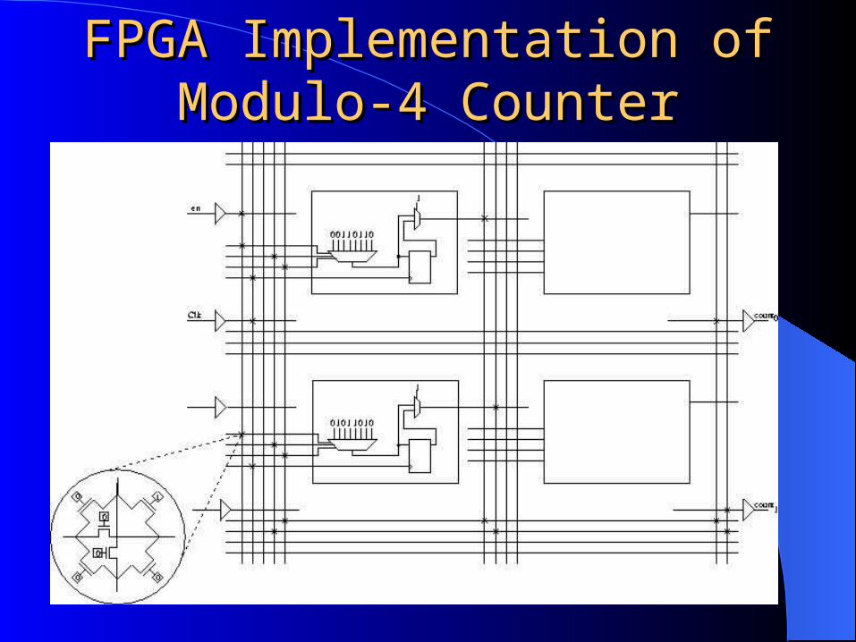
FPGA Implementation of FPGA Implementation of Modulo-4 CounterModulo-4 Counter
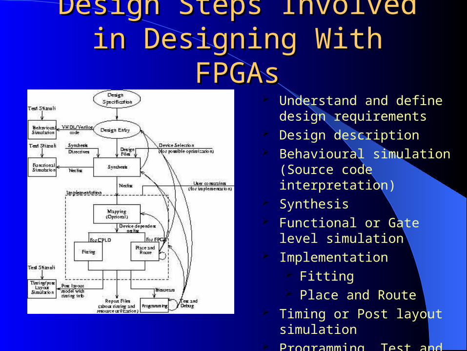
Design Steps Involved in Design Steps Involved in Designing With FPGAsDesigning With FPGAs
Understand and define design requirements
Design description Behavioural simulation (Source
code interpretation) Synthesis Functional or Gate level
simulation Implementation
Fitting Place and Route
Timing or Post layout simulation
Programming, Test and Debug
Commercially Available Commercially Available DevicesDevices
Architecture differs from vendor to vendor
Characterized by Structure and content of logic block Structure and content of routing resources
To examine, look at some of available devices FPGA: Xilinx (XC4000) CPLD: Altera (MAX 5K)
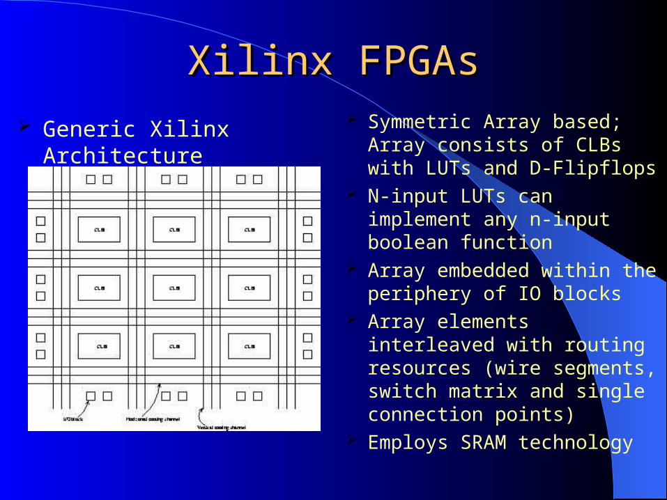
Xilinx FPGAsXilinx FPGAs Symmetric Array based;
Array consists of CLBs with LUTs and D-Flipflops
N-input LUTs can implement any n-input boolean function
Array embedded within the periphery of IO blocks
Array elements interleaved with routing resources (wire segments, switch matrix and single connection points)
Employs SRAM technology
Generic Xilinx Architecture
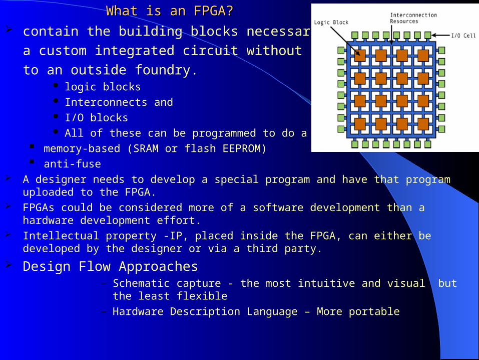
What is an FPGA?What is an FPGA? contain the building blocks necessary to design
a custom integrated circuit without having to turn
to an outside foundry. logic blocks Interconnects and I/O blocks All of these can be programmed to do a particular function
memory-based (SRAM or flash EEPROM) anti-fuse
A designer needs to develop a special program and have that program uploaded to the FPGA. FPGAs could be considered more of a software development than a hardware development
effort. Intellectual property -IP, placed inside the FPGA, can either be developed by the designer or via
a third party.
Design Flow Approaches – Schematic capture - the most intuitive and visual but the least flexible – Hardware Description Language – More portable
Why FPGAs?Why FPGAs? Advantages of FPGAs
Replacement of SSI and MSI chips Availability of parts off the shelf Rapid Turnaround Low risk Re programmability
Limitations PLDs will operate faster than FPGAs for the same design
implemented in both For FPGAs the circuit delay depends on the design
implementation tools Less dense and operate at lower speed when compared
to conventional Gate Arrays
FPGA manufacturersXilinx (http://www.xilinx.com) SRAM-
based FPGAs ( tens of thousands to millions upon millions of gates).
Altera (http://www.altera.com) SRAM based FPGAs
Lattice Semiconductor (http://www.latticesemi.com)
Actel (http://www.actel.com)Quick Logic (http://www.quicklogic.com)
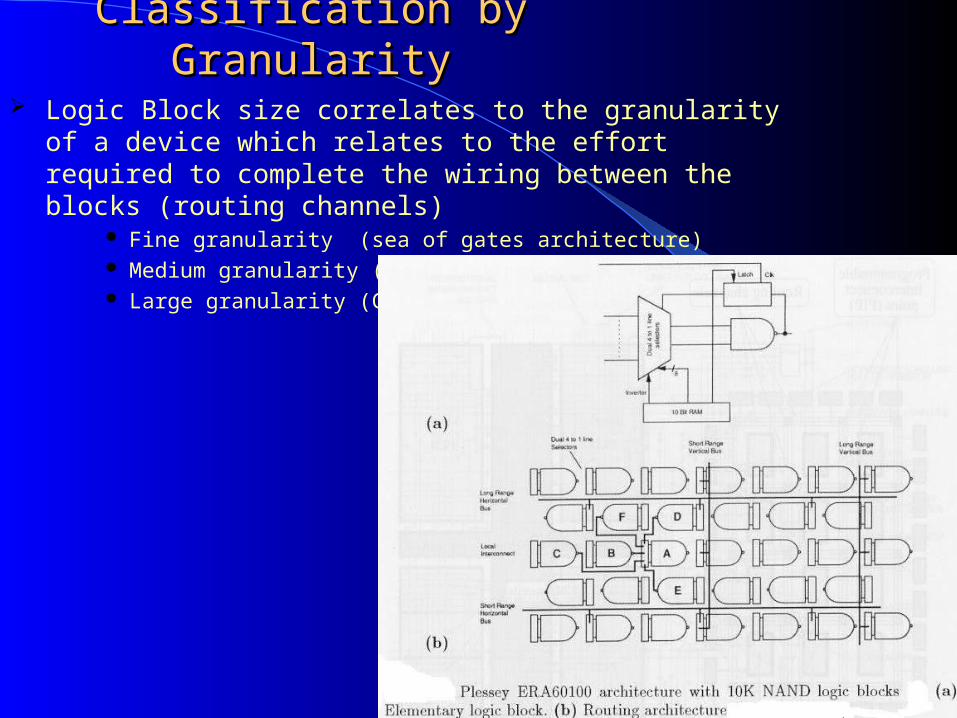
Classification by GranularityClassification by Granularity
Logic Block size correlates to the granularity of a device which relates to the effort required to complete the wiring between the blocks (routing channels)
Fine granularity (sea of gates architecture) Medium granularity (FPGA) Large granularity (CPLD)
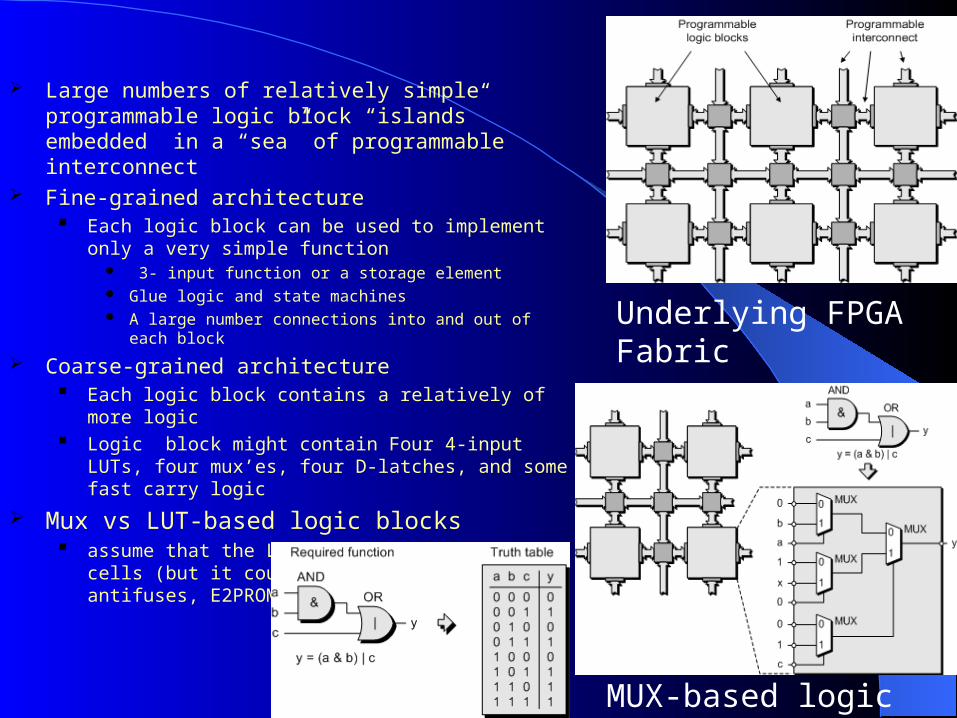
Large numbers of relatively simple programmable logic block “islands” embedded in a “sea” of programmable interconnect
Fine-grained architecture Each logic block can be used to implement only a very
simple function 3- input function or a storage element Glue logic and state machines A large number connections into and out of each block
Coarse-grained architecture Each logic block contains a relatively of more logic Logic block might contain Four 4-input LUTs, four mux’es,
four D-latches, and some fast carry logic
Mux vs LUT-based logic blocks assume that the LUT is formed from SRAM cells (but it
could be formed using antifuses, E2PROM, or FLASH cells)
Underlying FPGA Fabric
MUX-based logic block
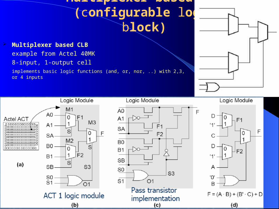
Multiplexer based CLB (configurable logic block)
Multiplexer based CLB
example from Actel 40MK
8-input, 1-output cellimplements basic logic functions (and, or, nor, ..) with 2,3, or 4 inputs
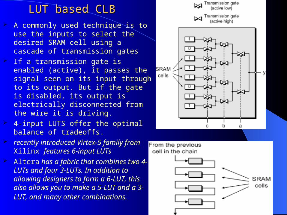
LUT based CLBLUT based CLB A commonly used technique is to use the
inputs to select the desired SRAM cell using a cascade of transmission gates
If a transmission gate is enabled (active), it passes the signal seen on its input through to its output. But if the gate is disabled, its output is electrically disconnected from the wire it is driving.
4-input LUTS offer the optimal balance of tradeoffs.
recently introduced Virtex-5 family from Xilinx features 6-input LUTs
Altera has a fabric that combines two 4-LUTs and four 3-LUTs. In addition to allowing designers to form a 6-LUT, this also allows you to make a 5-LUT and a 3-LUT, and many other combinations.
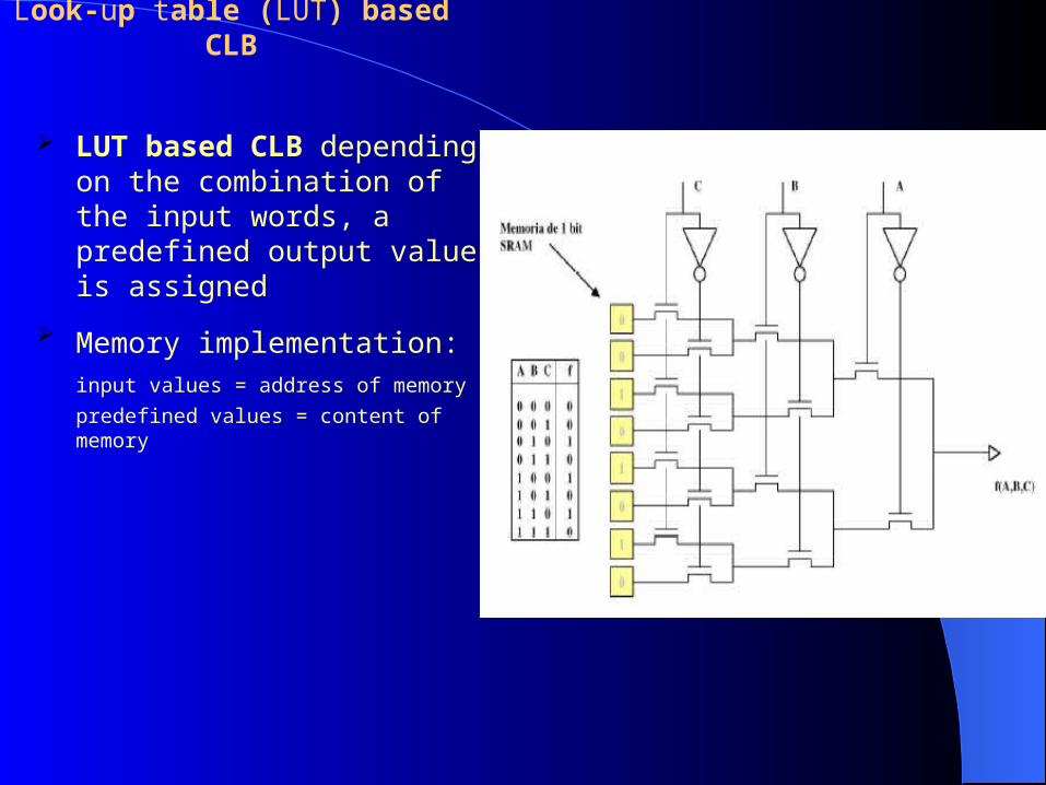
Look-up table (LUT) based CLB
LUT based CLB depending on the combination of the input words, a predefined output value is assigned
Memory implementation: input values = address of memory
predefined values = content of memory
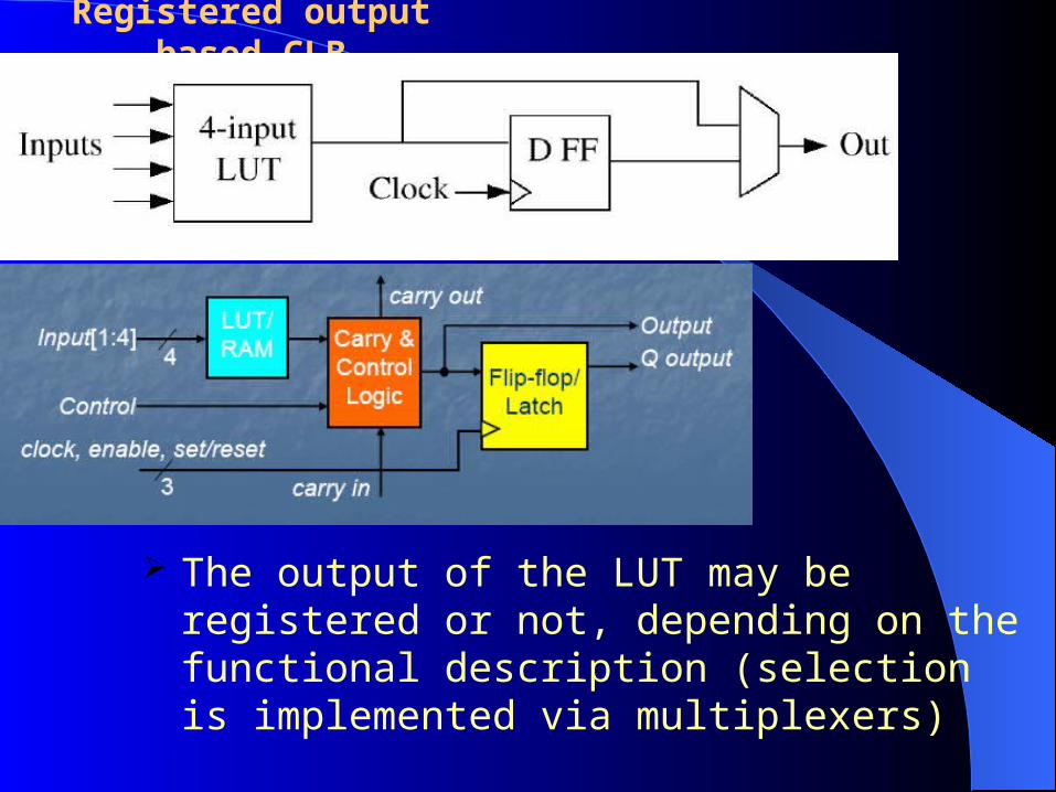
Registered output based CLB
The output of the LUT may be registered or not, depending on the functional description (selection is implemented via multiplexers)
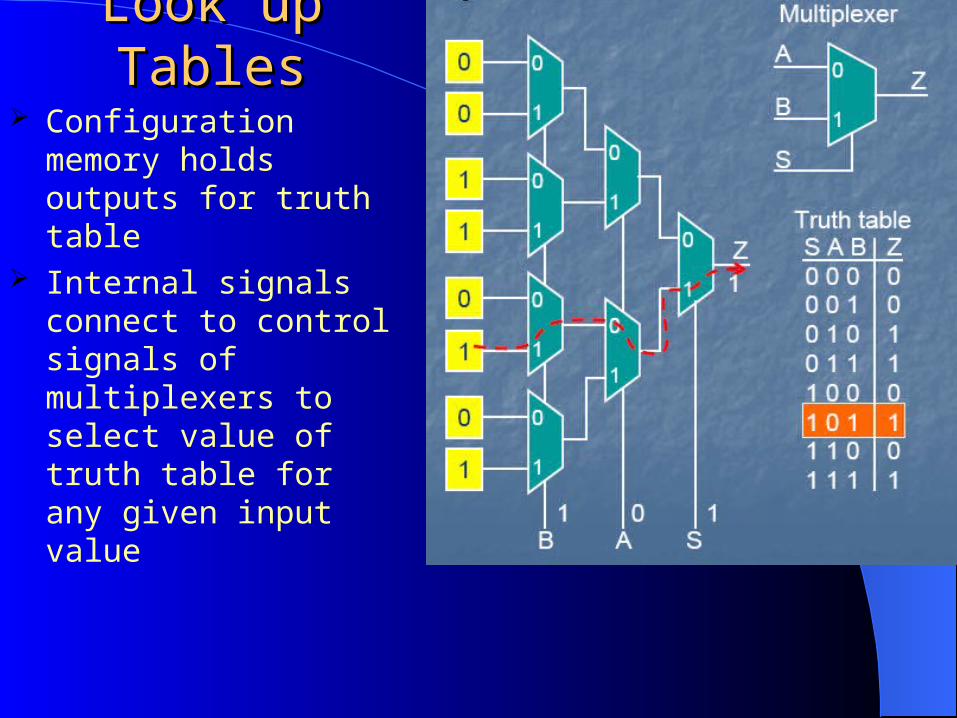
Look up TablesLook up Tables Configuration memory
holds outputs for truth table
Internal signals connect to control signals of multiplexers to select value of truth table for any given input value
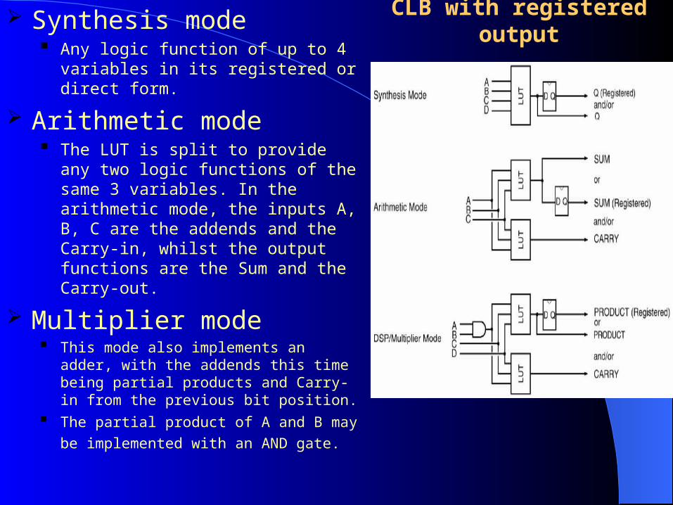
CLB with registered output Synthesis mode Any logic function of up to 4 variables in
its registered or direct form.
Arithmetic mode The LUT is split to provide any two
logic functions of the same 3 variables. In the arithmetic mode, the inputs A, B, C are the addends and the Carry-in, whilst the output functions are the Sum and the Carry-out.
Multiplier mode This mode also implements an adder, with
the addends this time being partial products and Carry-in from the previous bit position.
The partial product of A and B may be
implemented with an AND gate.
CLB with registered output
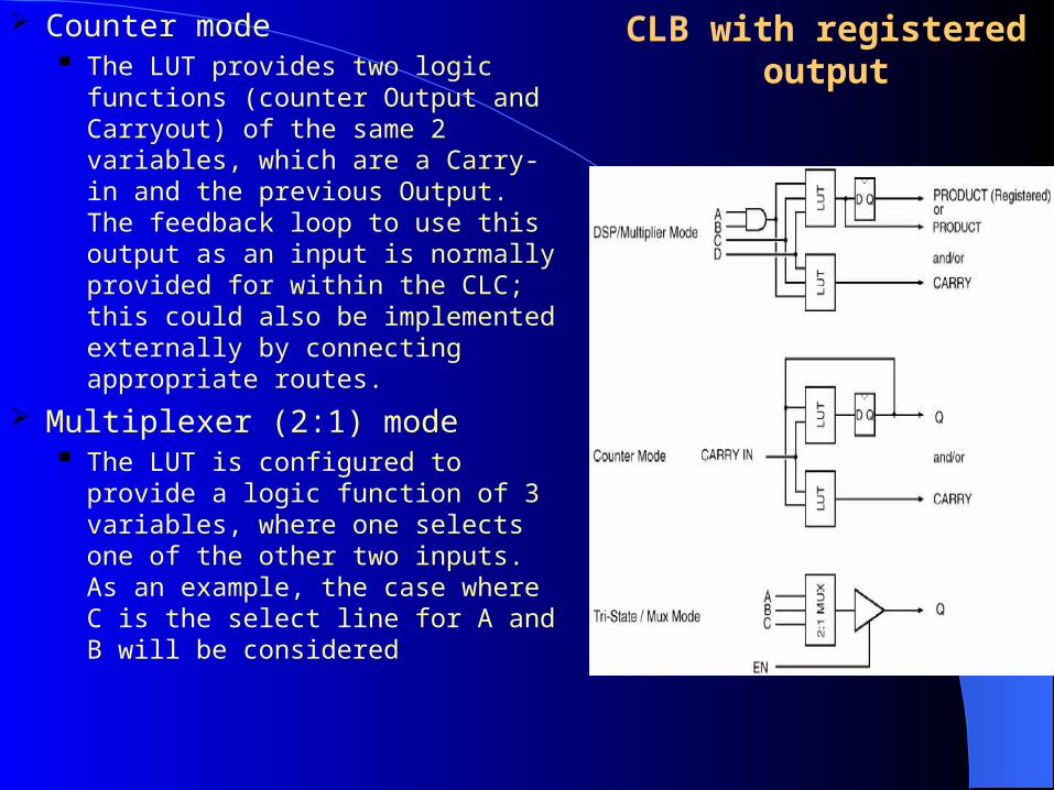
Counter mode The LUT provides two logic
functions (counter Output and Carryout) of the same 2 variables, which are a Carry-in and the previous Output. The feedback loop to use this output as an input is normally provided for within the CLC; this could also be implemented externally by connecting appropriate routes.
Multiplexer (2:1) mode The LUT is configured to provide a
logic function of 3 variables, where one selects one of the other two inputs. As an example, the case where C is the select line for A and B will be considered
An ExampleAn Example
Modulo-4 counter: Specification
Modulo-4 counter: Logic Implementation
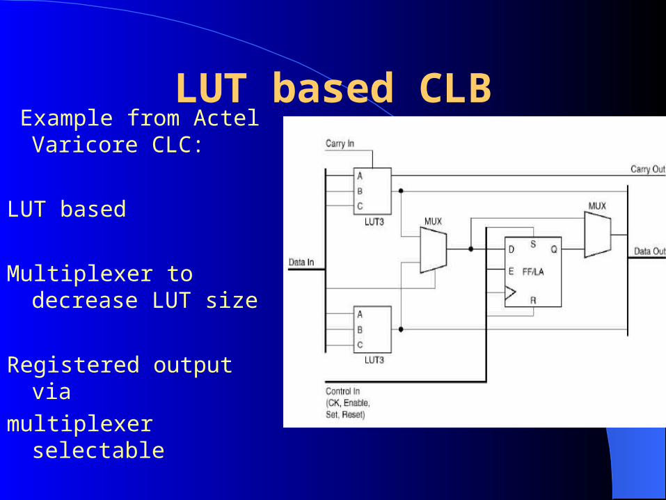
LUT based CLB Example from Actel
Varicore CLC:
LUT based
Multiplexer to decrease LUT size
Registered output via
multiplexer selectable
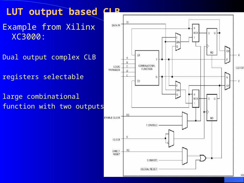
LUT output based CLB
Example from Xilinx XC3000:
Dual output complex CLB
registers selectable
large combinational
function with two outputs
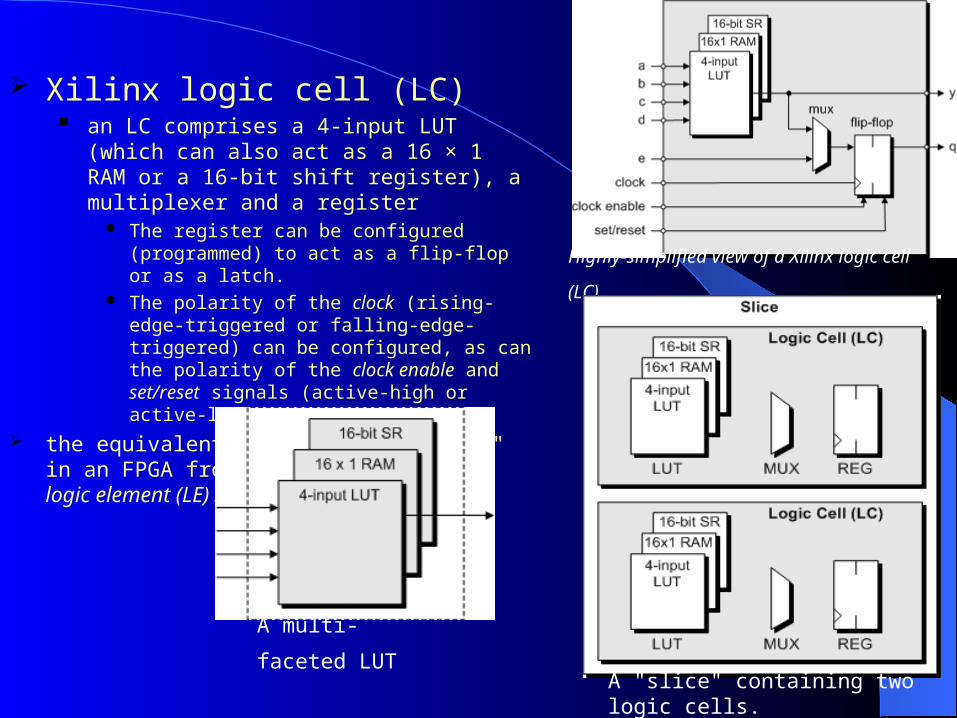
Xilinx logic cell (LC) an LC comprises a 4-input LUT (which can
also act as a 16 × 1 RAM or a 16-bit shift register), a multiplexer and a register
The register can be configured (programmed) to act as a flip-flop or as a latch.
The polarity of the clock (rising-edge-triggered or falling-edge-triggered) can be configured, as can the polarity of the clock enable and set/reset signals (active-high or active-low)
the equivalent core "building block" in an FPGA from Altera is called a logic element (LE).
Highly-simplified view of a Xilinx logic cell (LC).
A "slice" containing two logic cells.
A multi-faceted LUT
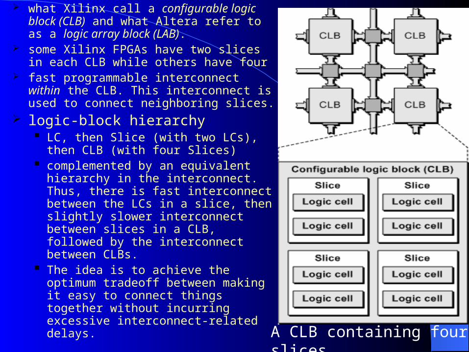
what Xilinx call a configurable logic block (CLB) and what Altera refer to as a logic array block (LAB).
some Xilinx FPGAs have two slices in each CLB while others have four
fast programmable interconnect within the CLB. This interconnect is used to connect neighboring slices.
logic-block hierarchy LC, then Slice (with two LCs), then
CLB (with four Slices) complemented by an equivalent
hierarchy in the interconnect. Thus, there is fast interconnect between the LCs in a slice, then slightly slower interconnect between slices in a CLB, followed by the interconnect between CLBs.
The idea is to achieve the optimum tradeoff between making it easy to connect things together without incurring excessive interconnect-related delays. A CLB containing four slices
all of the LUTs within a CLB can be configured together to implement the following: Single-port 16 × 8 bit RAM Single-port 32 × 4 bit RAM Single-port 64 × 2 bit RAM Single-port 128 × 1 bit RAM Dual-port 16 × 4 bit RAM Dual-port 32 × 2 bit RAM Dual-port 64 × 1 bit RAM
each 4-bit LUT can be used as a 16-bit shift register the LUTs within a single CLB to be configured together to implement a shift register
containing up to 128 bits as required Fast carry chains
A key feature - the special logic and interconnect required to implement fast carry chains. In the context of the CLBs, each logic cell (LC) contains special carry logic.
This is complemented by dedicated interconnect between the two LCs in each slice, between the slices in each CLB, and between the CLBs themselves.
This special carry logic and dedicated routing boosts the performance of logical functions such as counters and arithmetic functions such as adders.
The availability of these fast carry chains – in conjunction with features like the shift register incarnations of LUTs and the embedded multipliers.
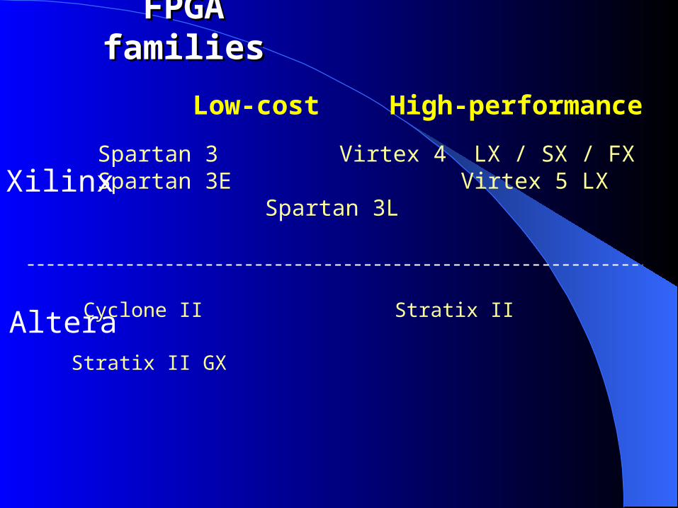
FPGFPGAA familiesfamilies
Spartan 3 Virtex 4 LX / SX / FX Spartan 3E Virtex 5 LX
Spartan 3L
Low-cost High-performance
Xilinx
Altera Cyclone II Stratix II
Stratix II GX
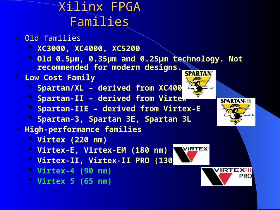
Xilinx FPGA FamiliesXilinx FPGA Families
Old families XC3000, XC4000, XC5200 Old 0.5µm, 0.35µm and 0.25µm technology. Not
recommended for modern designs. Low Cost Family
Spartan/XL – derived from XC4000 Spartan-II – derived from Virtex Spartan-IIE – derived from Virtex-E Spartan-3, Spartan 3E, Spartan 3L
High-performance families Virtex (220 nm) Virtex-E, Virtex-EM (180 nm) Virtex-II, Virtex-II PRO (130 nm) Virtex-4 (90 nm) Virtex 5 (65 nm)
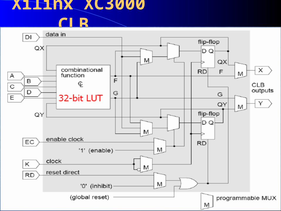
Xilinx XC3000 CLB
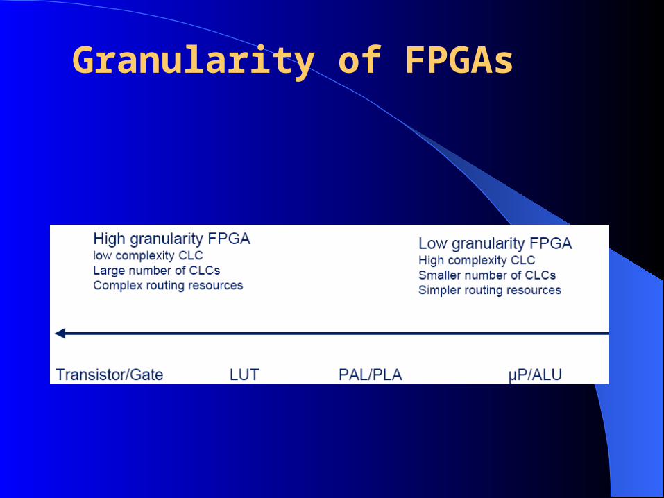
Granularity of FPGAs
an evolution of PAL’s where size is increased by an order of magnitude, or a refinement of mask-programmed gate arrays, where the reprogramming time and cost are drastically reduced
anti-fuse versus reprogrammable configuration, block-structured versus channel-structured routing, and lookup table (LUT) versus multiplexer versus sum-of-products logic.
the technology and architecture of the routing fabric is the most important factor in determining the effectiveness of an FPGA for a particular application.
Selection of an FPGASelection of an FPGA
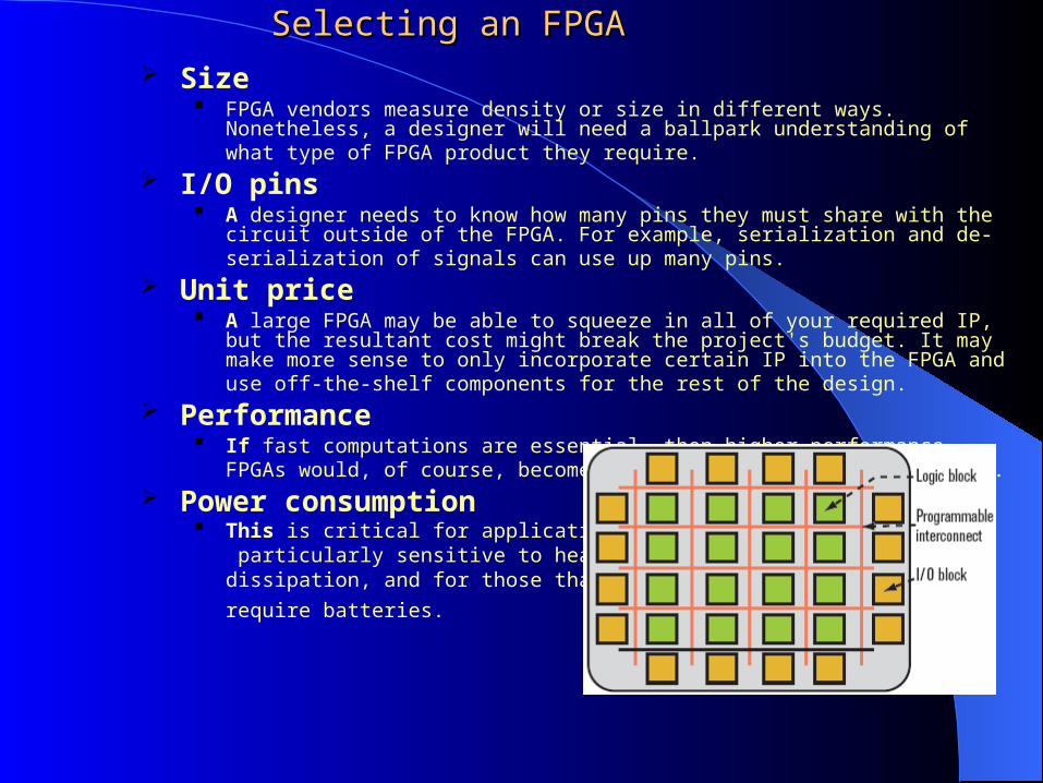
Selecting an FPGASelecting an FPGA
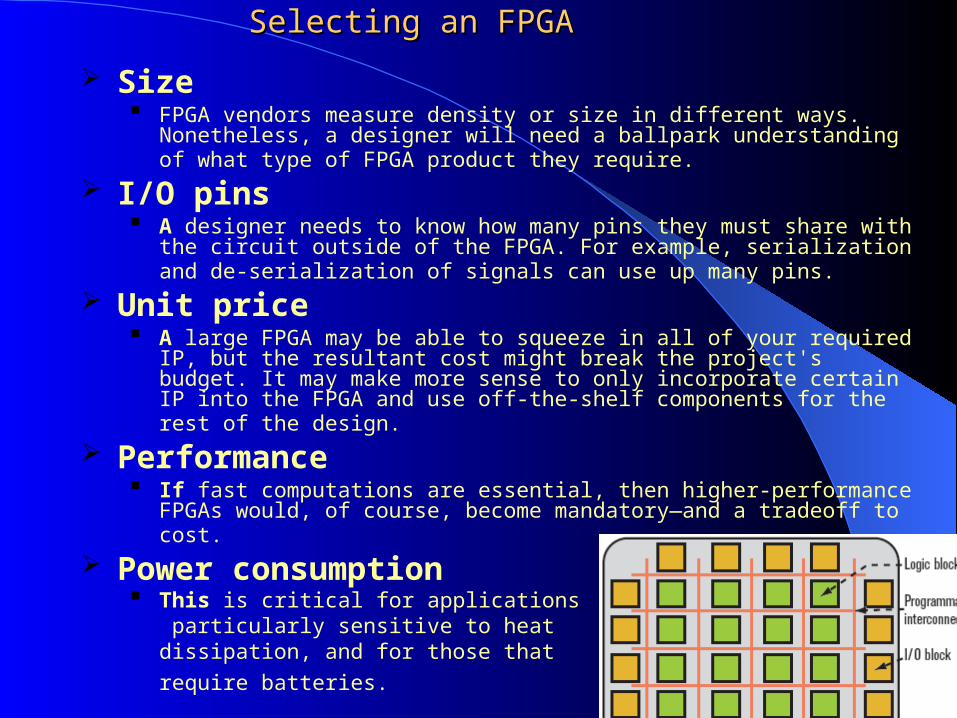
Size FPGA vendors measure density or size in different ways. Nonetheless, a
designer will need a ballpark understanding of what type of FPGA product they require.
I/O pins A designer needs to know how many pins they must share with the circuit
outside of the FPGA. For example, serialization and de-serialization of signals can use up many pins.
Unit price A large FPGA may be able to squeeze in all of your required IP, but the
resultant cost might break the project's budget. It may make more sense to only incorporate certain IP into the FPGA and use off-the-shelf components for the rest of the design.
Performance If fast computations are essential, then higher-performance FPGAs would, of
course, become mandatory—and a tradeoff to cost. Power consumption
This is critical for applications particularly sensitive to heat dissipation, and for those that
require batteries.
FPGA routing enables (almost) arbitrary connection among logic blocks, but at the cost of tying up more area and incurring more delay than present in a mask programmed part. Likewise,
the logic architectures of FPGA’s are larger and slower than mask defined gates, since their functionality must be programmable. But in comparison to the routing fabric, their delays tend to be more predictable and less of a limiting factor.
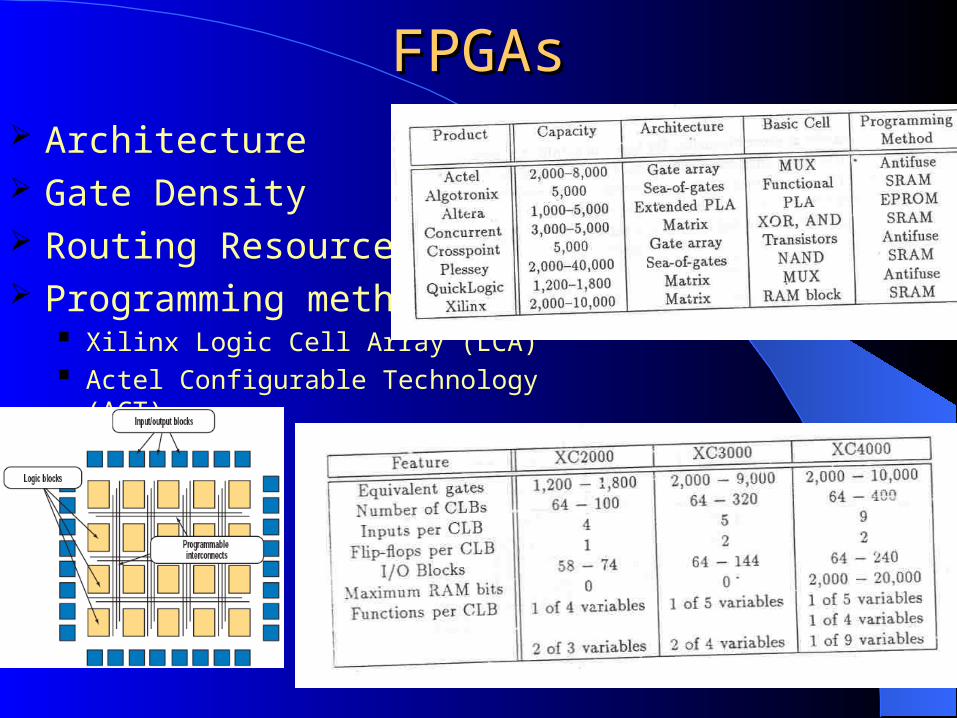
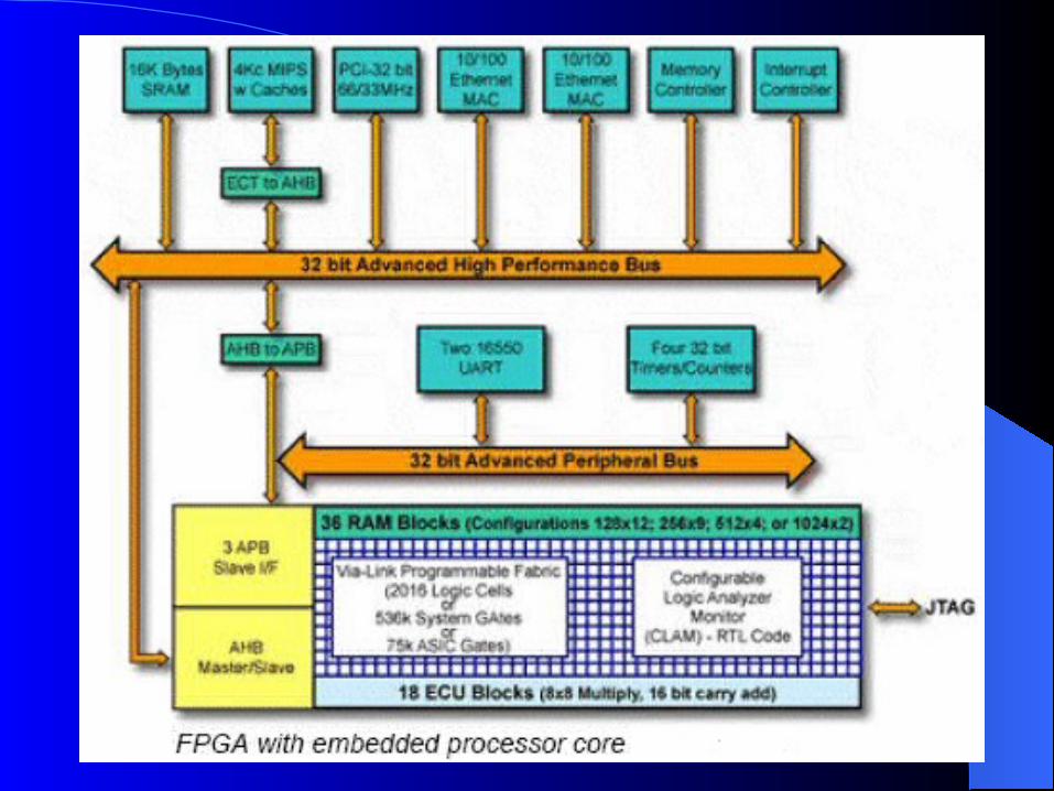
FPGAsFPGAs Architecture Gate Density Routing Resources Programming method
Xilinx Logic Cell Array (LCA) Actel Configurable Technology (ACT)
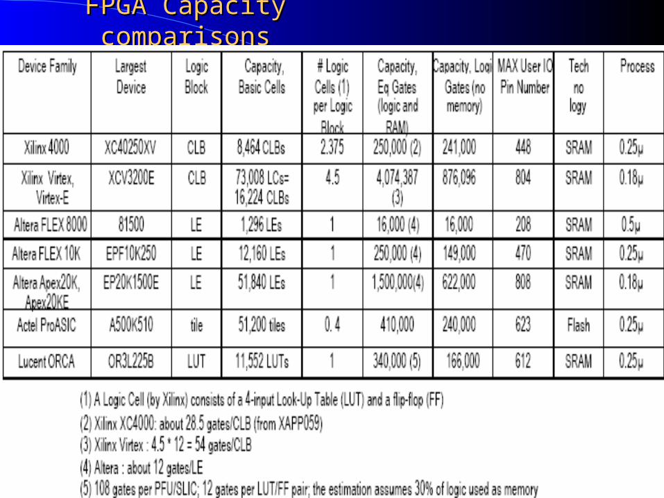
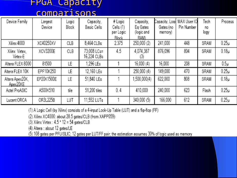
FPGA Capacity comparisonsFPGA Capacity comparisons
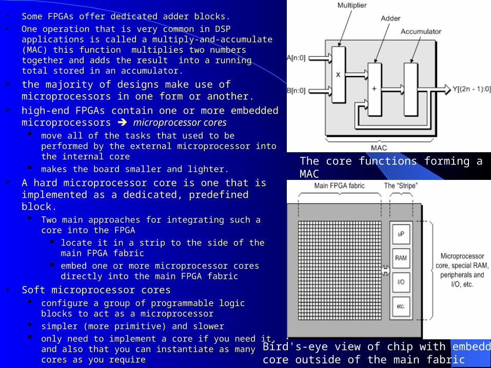
Some FPGAs offer dedicated adder blocks. One operation that is very common in DSP applications is
called a multiply-and-accumulate (MAC) this function multiplies two numbers together and adds the result into a running total stored in an accumulator.
the majority of designs make use of microprocessors in one form or another.
high-end FPGAs contain one or more embedded microprocessors microprocessor cores move all of the tasks that used to be performed by the
external microprocessor into the internal core makes the board smaller and lighter.
A hard microprocessor core is one that is implemented as a dedicated, predefined block. Two main approaches for integrating such a core into
the FPGA locate it in a strip to the side of the main FPGA
fabric embed one or more microprocessor cores directly
into the main FPGA fabric Soft microprocessor cores
configure a group of programmable logic blocks to act as a microprocessor
simpler (more primitive) and slower only need to implement a core if you need it, and also
that you can instantiate as many cores as you require
The core functions forming a MAC
Bird's-eye view of chip with embedded core outside of the main fabric
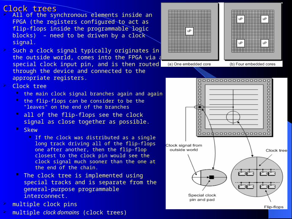
Clock treesClock trees All of the synchronous elements inside an FPGA
(the registers configured to act as flip-flops inside the programmable logic blocks) – need to be driven by a clock signal.
Such a clock signal typically originates in the outside world, comes into the FPGA via a special clock input pin, and is then routed through the device and connected to the appropriate registers.
Clock tree the main clock signal branches again and again the flip-flops can be consider to be the "leaves" on
the end of the branches
all of the flip-flops see the clock signal as close together as possible.
Skew If the clock was distributed as a single long track
driving all of the flip-flops one after another, then the flip-flop closest to the clock pin would see the clock signal much sooner than the one at the end of the chain.
The clock tree is implemented using special tracks and is separate from the general-purpose programmable interconnect.
multiple clock pins multiple clock domains (clock trees)
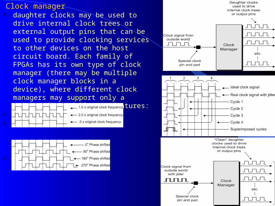
Clock managerClock manager daughter clocks may be used to drive internal
clock trees or external output pins that can be used to provide clocking services to other devices on the host circuit board. Each family of FPGAs has its own type of clock manager (there may be multiple clock manager blocks in a device), where different clock managers may support only a subset of the following features:
Jitter removal Frequency synthesis
Phase shifting
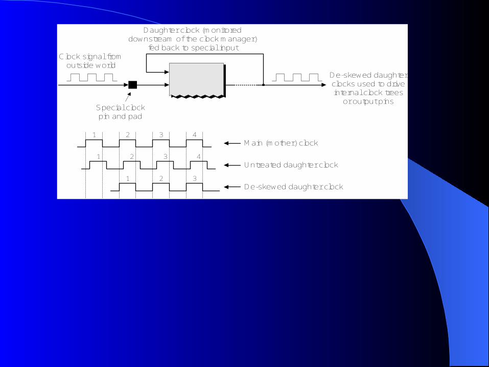
Main (mother) clock
Untreated daughter clock
De-skewed daughter clock
1 2 3 4
1 2 3 4
1 2 3
Clock signal fromoutside world
Special clockpin and pad
De-skewed daughterclocks used to driveinternal clock trees
or output pins
Daughter clock (monitoreddownstream of the clock manager)
fed back to special input
Selecting an FPGASelecting an FPGA Size
FPGA vendors measure density or size in different ways. Nonetheless, a designer will need a ballpark understanding of what type of FPGA product they require.
I/O pins A designer needs to know how many pins they must share with the circuit outside of
the FPGA. For example, serialization and de-serialization of signals can use up many pins.
Unit price A large FPGA may be able to squeeze in all of your required IP, but the resultant cost
might break the project's budget. It may make more sense to only incorporate certain IP into the FPGA and use off-the-shelf components for the rest of the design.
Performance If fast computations are essential, then higher-performance FPGAs would, of course,
become mandatory—and a tradeoff to cost. Power consumption
This is critical for applications particularly sensitive to heat dissipation, and for those that
require batteries.
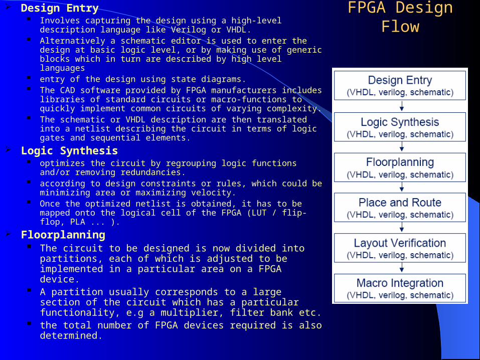
FPGA Design FlowFPGA Design Flow Design Entry
Involves capturing the design using a high-level description language like Verilog or VHDL.
Alternatively a schematic editor is used to enter the design at basic logic level, or by making use of generic blocks which in turn are described by high level languages
entry of the design using state diagrams. The CAD software provided by FPGA manufacturers includes
libraries of standard circuits or macro-functions to quickly implement common circuits of varying complexity.
The schematic or VHDL description are then translated into a netlist describing the circuit in terms of logic gates and sequential elements.
Logic Synthesis optimizes the circuit by regrouping logic functions and/or removing
redundancies. according to design constraints or rules, which could be minimizing
area or maximizing velocity. Once the optimized netlist is obtained, it has to be mapped onto
the logical cell of the FPGA (LUT / flip-flop, PLA ... ).
Floorplanning The circuit to be designed is now divided into partitions,
each of which is adjusted to be implemented in a particular area on a FPGA device.
A partition usually corresponds to a large section of the circuit which has a particular functionality, e.g a multiplier, filter bank etc.
the total number of FPGA devices required is also determined.
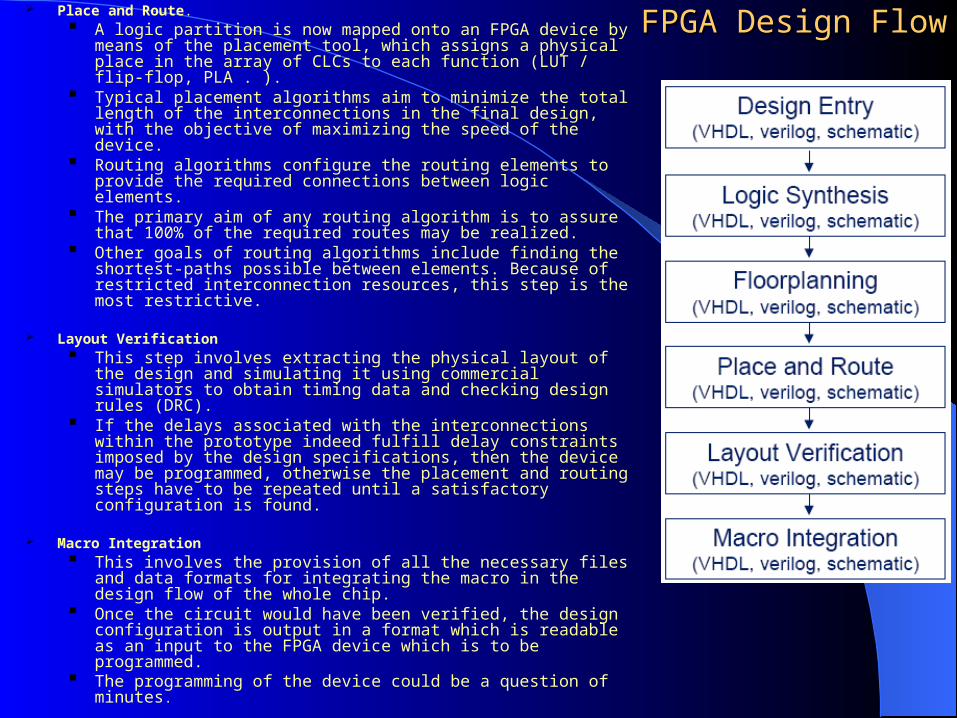
FPGA Design FlowFPGA Design Flow Place and Route.
A logic partition is now mapped onto an FPGA device by means of the placement tool, which assigns a physical place in the array of CLCs to each function (LUT / flip-flop, PLA . ).
Typical placement algorithms aim to minimize the total length of the interconnections in the final design, with the objective of maximizing the speed of the device.
Routing algorithms configure the routing elements to provide the required connections between logic elements.
The primary aim of any routing algorithm is to assure that 100% of the required routes may be realized.
Other goals of routing algorithms include finding the shortest-paths possible between elements. Because of restricted interconnection resources, this step is the most restrictive.
Layout Verification This step involves extracting the physical layout of the design
and simulating it using commercial simulators to obtain timing data and checking design rules (DRC).
If the delays associated with the interconnections within the prototype indeed fulfill delay constraints imposed by the design specifications, then the device may be programmed, otherwise the placement and routing steps have to be repeated until a satisfactory configuration is found.
Macro Integration This involves the provision of all the necessary files and data
formats for integrating the macro in the design flow of the whole chip.
Once the circuit would have been verified, the design configuration is output in a format which is readable as an input to the FPGA device which is to be programmed.
The programming of the device could be a question of minutes.
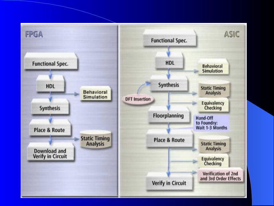
The Design CycleThe Design Cycle ASIC Design Methodology
the design is verified by simulation at each stage of refinement Accurate simulators are slow Fast simulators trade away simulation accuracy.
ASIC designers use a battery of simulators across the speed-accuracy spectrum in an attempt to verify the design.
an FPGA designer can replace simulation with in-circuit verification, “simulating” the circuitry in real time with a prototype The path from design to prototype is short, allowing a designer
to verify operation over a wide range of conditions at high speed and high accuracy.
proof-of-concept prototype designs easily Designs can be verified by trial rather than reduction to first principles
or by mental execution. verify that the design works in the real system, not merely in a
potentially-erroneous simulation model of the system.
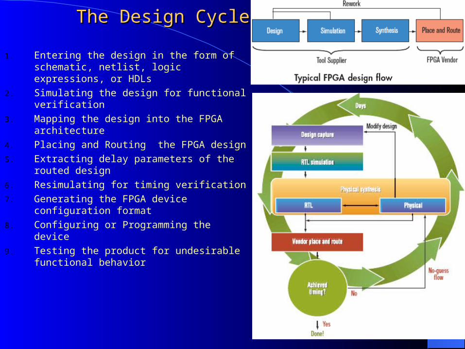
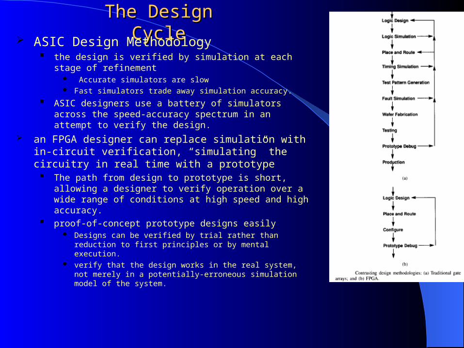
The Design CycleThe Design Cycle
1. Entering the design in the form of schematic, netlist, logic expressions, or HDLs
2. Simulating the design for functional verification
3. Mapping the design into the FPGA architecture
4. Placing and Routing the FPGA design
5. Extracting delay parameters of the routed design
6. Resimulating for timing verification
7. Generating the FPGA device configuration format
8. Configuring or Programming the device
9. Testing the product for undesirable functional behavior
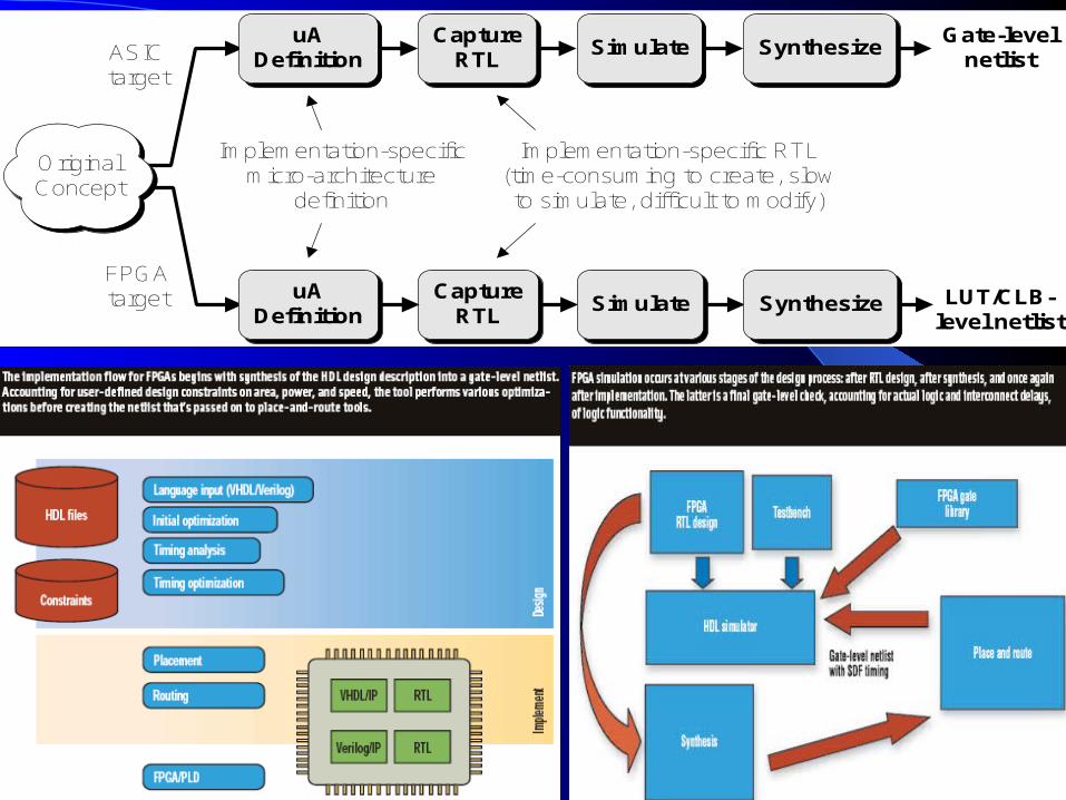
Implementation-specific RTL(time-consuming to create, slowto simulate, difficult to modify)
FPGAtarget
Gate-levelnetlist
LUT/CLB-level netlist
ASICtarget
OriginalConcept
CaptureRTL
Simulate Synthesize
CaptureRTL
Simulate Synthesize
uADefinition
uADefinition
Implementation-specificmicro-architecture
definition
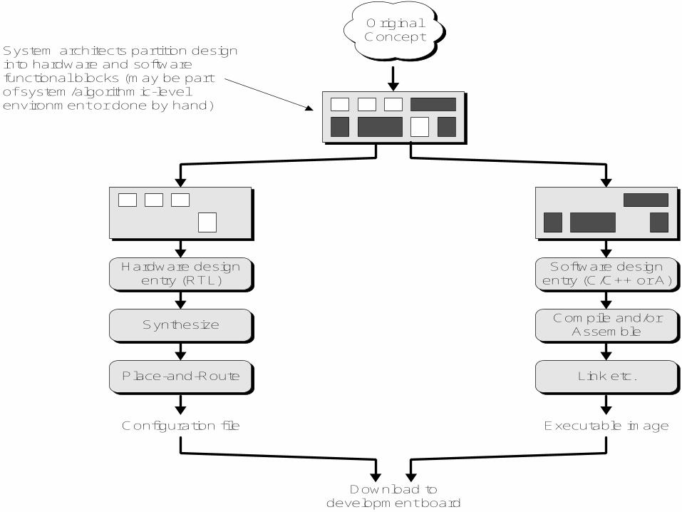
OriginalConcept
System architects partition designinto hardware and softwarefunctional blocks (may be partof system/algorithmic-levelenvironment or done by hand)
Hardware designentry (RTL)
SynthesizeCompile and/or
Assemble
Software designentry (C/C++ or A)
Place-and-Route Link etc.
Configuration file Executable image
Download todevelopment board
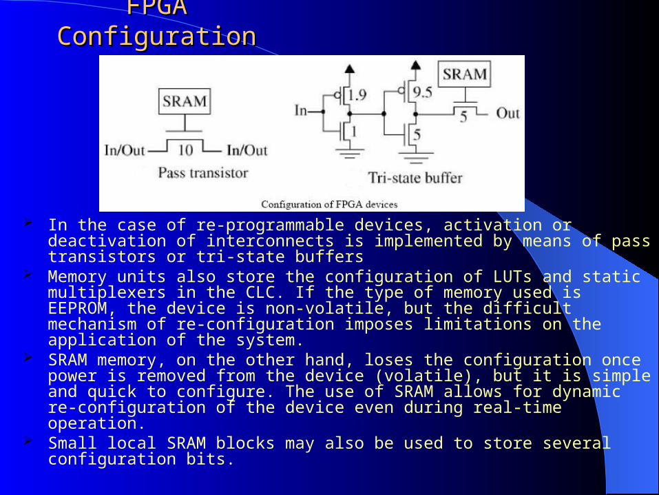
FPGA ConfigurationFPGA Configuration
In the case of re-programmable devices, activation or deactivation of interconnects is implemented by means of pass transistors or tri-state buffers
Memory units also store the configuration of LUTs and static multiplexers in the CLC. If the type of memory used is EEPROM, the device is non-volatile, but the difficult mechanism of re-configuration imposes limitations on the application of the system.
SRAM memory, on the other hand, loses the configuration once power is removed from the device (volatile), but it is simple and quick to configure. The use of SRAM allows for dynamic re-configuration of the device even during real-time operation.
Small local SRAM blocks may also be used to store several configuration bits.
FPGA Capacity comparisonsFPGA Capacity comparisons
SRAM FPGA -- EEPROM SRAM FPGA -- EEPROM FPGA FPGA
Despite this, however, most FPGAs still use SRAM for reasons of simplicity (when you need to reprogram it, it's easier to re-encode a small ROM chip than to reprogram a large FPGA chip), so count on having to use a separate boot ROM for the FPGA.
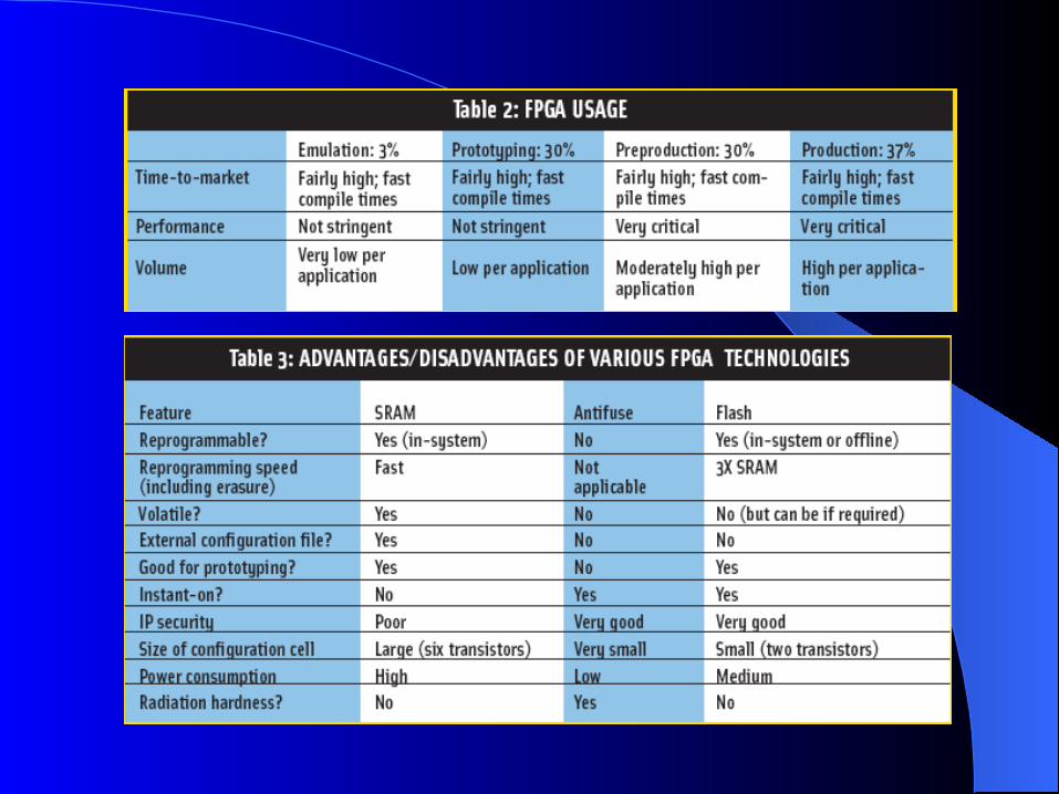
Use of an FPGA is broadly divided into two main stages:
Configuration mode the mode in which the FPGA is when you first power
it up. Configuration mode is, as you may have guessed, where you configure the FPGA;
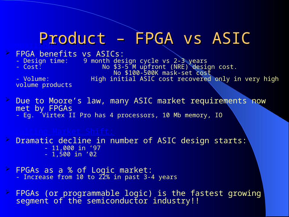
Product – FPGA vs ASICProduct – FPGA vs ASICComparison: FPGA benefits vs ASICs:
- Design time: 9 month design cycle vs 2-3 years- Cost: No $3-5 M upfront (NRE) design cost. No $100-500K mask-set cost- Volume: High initial ASIC cost recovered only in very high volume products
Due to Moore’s law, many ASIC market requirements now met by FPGAs- Eg. Virtex II Pro has 4 processors, 10 Mb memory, IO
Resulting Market Shift: Dramatic decline in number of ASIC design starts:
- 11,000 in ’97- 1,500 in ’02
FPGAs as a % of Logic market:- Increase from 10 to 22% in past 3-4 years
FPGAs (or programmable logic) is the fastest growing segment of the semiconductor industry!!
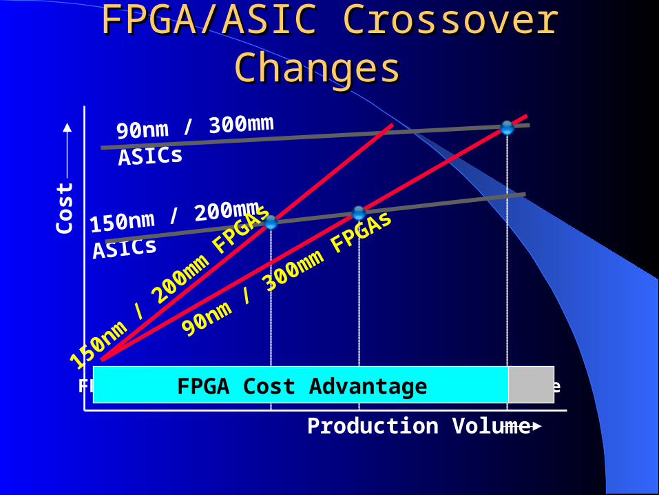
150nm / 200mm ASICs
FPGA/ASIC Crossover Changes FPGA/ASIC Crossover Changes
Production Volume
Cos
t
90nm / 300mm ASICs
150nm / 200mm FPGAs
90nm / 300mm FPGAs
FPGA Cost Advantage ASIC Cost AdvantageFPGA Cost Advantage ASIC Cost AdvantageFPGA Cost Advantage