Embed Size (px)
Citation preview
For Communications Equipment
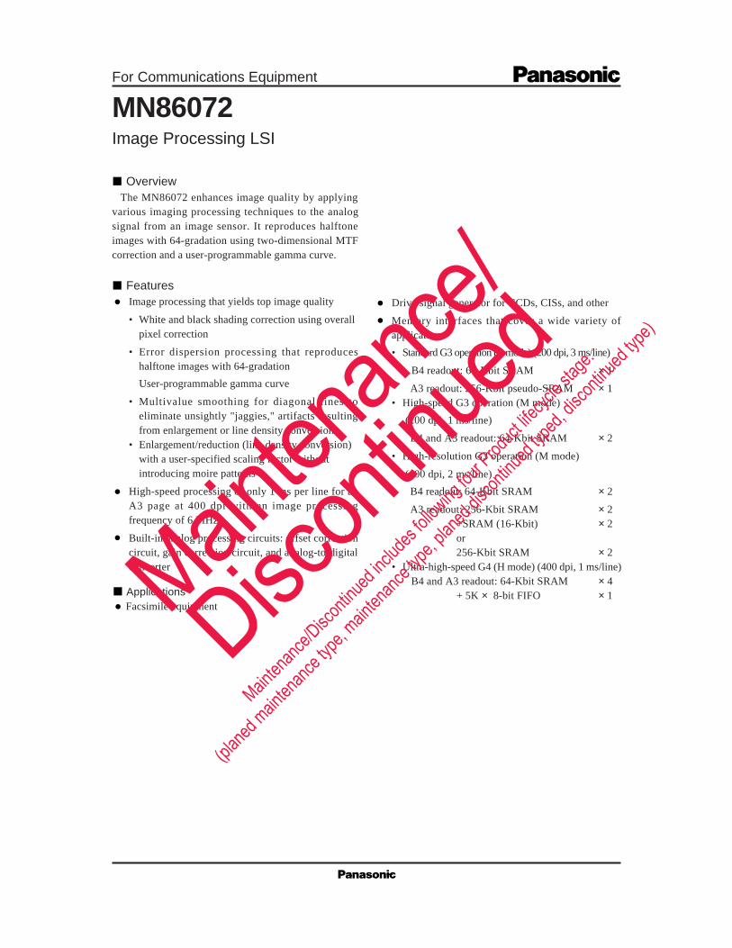
OverviewThe MN86072 enhances image quality by applying
various imaging processing techniques to the analogsignal from an image sensor. It reproduces halftoneimages with 64-gradation using two-dimensional MTFcorrection and a user-programmable gamma curve.
FeaturesImage processing that yields top image quality
• White and black shading correction using overallpixel correction
• Error dispersion processing that reproduceshalftone images with 64-gradation
User-programmable gamma curve
• Multivalue smoothing for diagonal lines toeliminate unsightly "jaggies," artifacts resultingfrom enlargement or line density conversion
• Enlargement/reduction (line density conversion)with a user-specified scaling factor withoutintroducing moire patterns
High-speed processing of only 1 ms per line for anA3 page at 400 dpi with an image processingfrequency of 6 MHz
Built-in analog processing circuits: offset correctioncircuit, gain correction circuit, and analog-to-digitalconverter
MN86072Image Processing LSI
Drive signal generator for CCDs, CISs, and other
Memory interfaces that cover a wide variety ofapplications
• Standard G3 operation (L mode) (200 dpi, 3 ms/line)
B4 readout: 64-Kbit SRAM × 1
A3 readout: 256-Kbit pseudo-SRAM × 1• High-speed G3 operation (M mode)
(200 dpi, 1 ms/line)
B4 and A3 readout: 64-Kbit SRAM × 2
• High-resolution G3 operation (M mode)
(400 dpi, 2 ms/line)
B4 readout: 64-Kbit SRAM × 2
A3 readout: 256-Kbit SRAM × 2+SRAM (16-Kbit) × 2or256-Kbit SRAM × 2
• Ultra-high-speed G4 (H mode) (400 dpi, 1 ms/line) B4 and A3 readout: 64-Kbit SRAM × 4
+ 5K × 8-bit FIFO × 1 ApplicationsFacsimile equipmentMain
tenan
ce/
Discon
tinued
Mainten
ance/D
iscont
inued
includ
es foll
owing
four P
roduct
lifecyc
le stag
e.
(planed
mainten
ance ty
pe, main
tenanc
e type,
planed
discon
tinued
typed,
discon
tinued
type)
MN86072 For Communications Equipment
Brief Specifications Image processing speed: • 0.1 to 6 million pixels per second Pixels per line: • max. 16,384 pixels in the primary scanning direction Offset correction: • negative feedback preamplifier
The chip controls the feedback voltage using A/D conversion data from black pixel sectionsBuilt-in circuits: Feedback voltage control circuit + source follower circuit × 2(Support for channel-separated CCDs included)
Gain control: • Analog control using an external operational amplifier and the built-in field effecttransistor (FET)
An external resistor determines the control range.(The standard range is from +6 dB to –12 dB.)Built-in circuits: Gain control circuit + FET × 2(Support for channel-separated CCDs included)
A/D converter: • Half flash converterNumber of bits: 8Conversion speed: 0.1 to 6 MHzInput range: min. 3 Vp-p
Input channels: Support for odd/even separation White shading correction: • Overall pixel correction
Distortion correction level: max. 75% (or max. 50%) of A/D converter's input range Black shading correction: • Overall pixel correction
Distortion correction level: 25% of A/D converter's input range MTF correction: • Laplacian transforms (processing for text images)
Reference to five pixels, max. coefficient of –1.875Support for edge direction-specific processing and processingfrom preceding history
Halftone processing:• Error dispersion processing: Reproduction of 64-gradation using 6-bit processing• Dither pattern: Mesh (4 × 4 or 8 × 8 pixels)
Bayer (4 × 4 pixels) Gamma correction: • User-definable by loading a conversion curve
Conversion levels: 7 bits to 6 Binary coded: • Fixed slice
Slice level: User-specified 5-bit value Enlargement/reduction (line density conversion):
• Decimation with image clock or line enableScaling factor in primary scanning direction: 0.78% to 200% (in 0.78% increments)Scaling factor in subscanning direction: 0.39% to 200% (in 0.39% increments)
Enlargement/reduction (line density conversion) correction:• Multivalue smoothing (for enlargement in primary direction or line density enchancement)• Black pixel preservation (for reduction in primary or subscanning direction or line
density reduction)• OR processing (for line density conversion in subscanning direction from 7.7 line/mm to
3.85) Sensor interfaces:
• CCD sensorSupports both channel-composite and channel-separated CCDs.Generates the following drive signals using user settings: FSG (SH), FCK1, FCK2(ø1 and ø2), FR1, FR2 (RS1 and RS2)
• Contacting bipolar image sensorGenerates SCLK and ST signals.
Mainten
ance/
Discon
tinued
Mainten
ance/D
iscont
inued
includ
es foll
owing
four P
roduct
lifecyc
le stag
e.
(planed
mainten
ance ty
pe, main
tenanc
e type,
planed
discon
tinued
typed,
discon
tinued
type)
For Communications Equipment MN86072
• CdS sensorGenerates SCLK and STPL signals.
Memory interfaces:• L mode (max. 1 MHz)
: 256-Kbit pseudo-SRAM × 1or256-Kbit SRAM × 1or, if enlargement and black shadingare disabled and the lines are not morethan 2048 pixels long, 64-Kbit SRAM × 1
• M mode(max.3MHz): 64-Kbit SRAM × 2
or, if there is enlargement or black shading64-Kbit SRAM × 3
• H mode (max. 6 MHz): 64-Kbit SRAM × 4
+ 5K × 8-bit FIFO × 1• Shading memory function (Common in L, M, and H modes)"
: Support for fixed ROM shading: Support for automatic data transfers between shading memory
and EEROM: Shading memory accessible from microprocessor for read/
write operations Image bus interface:
• Parallel mode (DMA slave operation): 8-bit mode: 16-bit mode (requires external circuitry)
• Serial mode with request (VREQ) input and enable (VSEN), clock (VSCK), anddata (VSDA) outputs
Scanning modes: • Free Scan• Cycle scan (normal drive)• Cycle scan (trapezoidal drive)• Trigger scan
System interface:• Interface to 8-bit microprocessors
(Choice of Intel or Motorola formats) Video data register readout function:
• Image data after A/D conversion or shading correction: Maximum value for ABC interval: Minimum value for offset correction interval: Data at user's choice of position
Image data I/O function:• Image data output after shading correction (8 bits)• Image data output after multivalue smoothing (7 bits)• Image data input sent from external A/D converter (8 bits)
Output ports: • 16 pins (memory interface for L mode)• 3 pins (memory interface for M mode)
Power supply: • Digital circuits DVDD: 5.0V• Analog circuits AVDD: 5.0V• A/D converter reference voltages VREFH: 5.0 to 3.0 V
VREFL: 0.0 to 2.0 V
Mainten
ance/
Discon
tinued
Mainten
ance/D
iscont
inued
includ
es foll
owing
four P
roduct
lifecyc
le stag
e.
(planed
mainten
ance ty
pe, main
tenanc
e type,
planed
discon
tinued
typed,
discon
tinued
type)
MN86072 For Communications Equipment
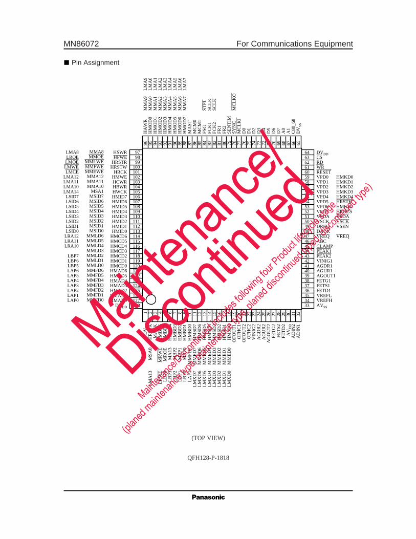
Pin Assignment
QFH128-P-1818
(TOP VIEW)
HSWRHFWE
HRSTRHRSTW
HRCKHMWEHCWRHBWRHWCKHMID7HMID6HMID5HMID4HMID3HMID2HMID1HMID0
HMCD6HMCD5HMCD4HMCD3HMCD2HMCD1HMCD0HMAD6HMAD5HMAD4HMAD3HMAD2HMAD1HMAD0
DVDD
MMA8MMOE
MMLWEMMFWEMMEWEMMA12MMA11MMA10
MSA1MSID7MSID6MSID5MSID4MSID3MSID2MSID1MSID0
MMLD6MMLD5MMLD4MMLD3MMLD2MMLD1MMLD0MMFD6MMFD5MMFD4MMFD3MMFD2MMFD1MMFD0
LMA8LROELMOELMWELMCE
LMA12LMA11LMA10LMA14LSID7LSID6LSID5LSID4LSID3LSID2LSID1LSID0
LRA12LRA11LRA10
LBP7LBP6LBP5LAP6LAP5LAP4LAP3LAP2LAP1LAP0
DVDDCSRDWRRESETVPD0VPD1VPD2VPD3VPD4VPD5VPD6VPD7VSDAVSCKDREQDACKVREQABCCLAMPPEAK1PEAK2VINIG1AGDR1AGUR1AGOUT1FETG1FETS1FETD1VREFLVREFHAVSS
HMKD0HMKD1HMKD2HMKD3HMKD4HRSTKHMKWHROCSVSDAVSCKVSEN
VREQ
979899
100101102103104105106107108109110111112113114115116117118119120121122123124125126127128
6463626160595857565554535251504948474645444342414039383736353433
HA
WR
HM
OD
0H
MO
D1
HM
OD
2H
MO
D3
HM
OD
4H
MO
D5
HM
OD
6H
MO
D7
MA
STM
CM
0M
CM
1FS
GFC
K1
FCK
2FR
1FR
2SE
NT
IMSY
NC
MC
LK
ID
0D
1D
2D
3D
4D
5D
6D
7A
0A
1C
80_6
8D
VSS
DV
SSH
RST
AM
AC
KH
MB
D6
HM
BD
5H
MB
D4
HM
BD
3H
MB
D2
HM
BD
1H
MB
D0
HM
SD7
HM
SD6
HM
SD5
HM
SD4
HM
SD3
HM
SD2
HM
SD1
HM
SD0
OFO
UT
1O
FHC
1O
FOU
T2
OFH
C2
VIN
IG2
AG
DR
2A
GU
R2
AG
OU
T2
FET
G2
FET
S2FE
TD
2A
VD
DA
DIN
2A
DIN
1
MSA
0
MR
WE
MR
OE
MA
13M
BP2
MB
P1M
BP0
MM
FD7
MM
ED
7M
ME
D6
MM
ED
5M
ME
D4
MM
ED
3M
ME
D2
MM
ED
1M
ME
D0
LM
A13
LR
WE
LB
P4L
BP3
LB
P2L
BP1
LB
P0L
AP7
LM
XD
7L
MX
D6
LM
XD
5L
MX
D4
LM
XD
3L
MX
D2
LM
XD
1L
MX
D0
MM
A9
MM
A0
MM
A1
MM
A2
MM
A3
MM
A4
MM
A5
MM
A6
MM
A7
STPL
SCL
KSC
LK
MC
LK
O
LM
A9
LM
A0
LM
A1
LM
A2
LM
A3
LM
A4
LM
A5
LM
A6
LM
A7
1 2 3 4 5 6 7 8 9 10 11 12 13 14 15 16 17 18 19 20 21 22 23 24 25 26 27 28 29 30 31 32
96 95 94 93 92 91 90 89 88 87 86 85 84 83 82 81 80 79 78 77 76 75 74 73 72 71 70 69 68 67 66 65
Mainten
ance/
Discon
tinued
Mainten
ance/D
iscont
inued
includ
es foll
owing
four P
roduct
lifecyc
le stag
e.
(planed
mainten
ance ty
pe, main
tenanc
e type,
planed
discon
tinued
typed,
discon
tinued
type)

For Communications Equipment MN86072
Pin Function Chart
HSWRHAWRHBWRHCWRHMWEHRSTAHWCKHRCKHRSTWHRSTRHFWEMACK
128pin QFH
VREQDACKDREQVSCKVSDA
VREQDACKVSENVSCKVSDA
HMKD0HMKD1HMKD2HMKD3HMKD4HRSTKHMKWHROCS
VPD0VPD1VPD2VPD3VPD4VPD5VPD6VPD7
VSCD0VSCD1VSCD2VSCD3VSCD4VSCD5VSCD6VSCD7
VGSD0VGSD1VGSD2VGSD3VGSD4VGSD5VGSD6CKVG
VADD0VADD1VADD2VADD3VADD4VADD5VADD6VADD7
HMSD0HMSD1HMSD2HMSD3HMSD4HMSD5HMSD6HMSD7
MMED0MMED1MMED2MMED3MMED4MMED5MMED6MMED7
LMXD0LMXD1LMXD2LMXD3LMXD4LMXD5LMXD6LMXD7
HMAD0HMAD1HMAD2HMAD3HMAD4HMAD5HMAD6
MMFD0MMFD1MMFD2MMFD3MMFD4MMFD5MMFD6
LAP0LAP1LAP2LAP3LAP4LAP5LAP6
HMBD0HMBD1HMBD2HMBD3HMBD4HMBD5HMBD6
MMFD7MBP0MBP1MBP2MA13MROEMRWE
LAP7LBP0LBP1LBP2LBP3LBP4LRWE
HMCD0HMCD1HMCD2HMCD3HMCD4HMCD5HMCD6
MMLD0MMLD1MMLD2MMLD3MMLD4MMLD5MMLD6
LBP5LBP6LBP7
LRA10LRA11LRA12
HMID0HMID1HMID2HMID3HMID4HMID5HMID6HMID7
MSID0MSID1MSID2MSID3MSID4MSID5MSID6MSID7
LSID0LSID1LSID2LSID3LSID4LSID5LSID6LSID7
HMOD0HMOD1HMOD2HMOD3HMOD4HMOD5HMOD6HMOD7
MMA0MMA1MMA2MMA3MMA4MMA5MMA6MMA7
LMA0LMA1LMA2LMA3LMA4LMA5LMA6LMA7
MMA8MMA9MMA10MMA11MMA12MSA0MSA1MMEWEMMFWEMMLWEMMOE
LMA8LMA9LMA10LMA11LMA12LMA13LMA14LMCELMWELMOELROE
MASTMCM0MCM1
D0D1D2D3D4D5D6D7A0A1CSWR(DS)RD(R/W)C80_68
MCLKISYNCMCLKO
FCK2FCK1FR1FR2FSGSENTIM
SCLKSCLK
STPL
PEAK1PEAK2CLAMPABC
OFOUT1OFHC1ADIN1FETS1FETD1FETG1AGOUT1AGUR1AGDR1VINIG1
VINIG2AGDR2AGUR2AGOUT2FETG2FETD2FETS2ADIN2OFHC2OFOUT2
VREFHVREFL
AVDDAVSS
DVDDDVDDDVSSDVSS
MN
8607
2
Mod
e se
lect
ion
(3)
Syst
em in
terf
ace
(15)
Clo
ck (
2)Se
nsor
inte
rfac
e (6
)A
nalo
g C
NT
(4)
Ana
log
pins
(20
)Po
wer
sup
ply
(8)
Imag
e bu
s in
terf
ace
(5)
Para
llel I
/O (
8)M
emor
y in
terf
ace
(5)
RESET
Mainten
ance/
Discon
tinued
Mainten
ance/D
iscont
inued
includ
es foll
owing
four P
roduct
lifecyc
le stag
e.
(planed
mainten
ance ty
pe, main
tenanc
e type,
planed
discon
tinued
typed,
discon
tinued
type)
MN86072 For Communications Equipment
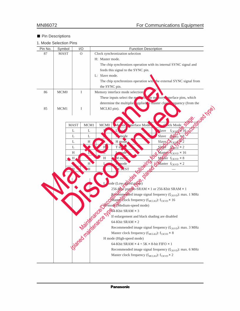
87 MAST O Clock synchronization selection
H: Master mode.
The chip synchronizes operation with its internal SYNC signal and
feeds this signal to the SYNC pin.
L: Slave mode.
The chip synchronizes operation with the external SYNC signal from
the SYNC pin.
86 MCM0 I Memory interface mode selection
These inputs select the mode for the memory interface pins, which
determine the multiplier applied to master clock frequency (from the
85 MCM1 I MCLKI pin).
MAST MCM1 MCM0 Memory Interface Mode Clock Mode
L L L L mode Slave fCKVD × 16
L L H M mode Slave fCKVD × 8
L H L H mode Slave fCKVD × 2
L H H T mode Slave fCKVD × 2
H L L L mode Master fCKVD × 16
H L H M mode Master fCKVD × 8
H H L H mode Master fCKVD × 2
H H H DCTEST —
1. Mode Selection Pins
Pin No. Symbol I/O Function Description
Pin Descriptions
L mode (Low-speed mode)
256-Kbit pseudo-SRAM × 1 or 256-Kbit SRAM × 1
Recommended image signal frequency (fCKVD): max. 1 MHz
Master clock frequency (fMCLKI ): fCKVD × 16
M mode (Medium-speed mode)
64-Kbit SRAM × 3
If enlargement and black shading are disabled
64-Kbit SRAM × 2
Recommended image signal frequency (fCKVD): max. 3 MHz
Master clock frequency (fMCLKI ): fCKVD × 8
H mode (High-speed mode)
64-Kbit SRAM × 4 + 5K × 8-bit FIFO × 1
Recommended image signal frequency (fCKVD): max. 6 MHz
Master clock frequency (fMCLKI ): fCKVD × 2
Mainten
ance/
Discon
tinued
Mainten
ance/D
iscont
inued
includ
es foll
owing
four P
roduct
lifecyc
le stag
e.
(planed
mainten
ance ty
pe, main
tenanc
e type,
planed
discon
tinued
typed,
discon
tinued
type)

For Communications Equipment MN86072
T mode (Test data input mode)
This mode is for testing internal functions.
Master clock frequency (fMCLKI ): fCKVD × 2
DCTEST mode
This mode configures the output and I/O pins for DC testing.
HMID0 HMID1 DC Test Function
0 — Output high-impedance test
1 0 "L" level output test
1 1 "H" level output test
1. Mode Selection Pins (continued)
Pin No. Symbol I/O Function Description
Pin Descriptions (continued)
76 to 69 D0 to D7 I/O Microprocessor data I/O bus
68, 67 A0, A1 I Microprocessor address input
63 CS IMicroprocessor chip select input
61 WR(DS) I Microprocessor data write input (Set C80_68 pin at "H" level)
Microprocessor data strobe input (Set C80_68 pin at "L" level)
62 RD(R/W) I Microprocessor data read input (Set C80_68 pin at "H" level)
Microprocessor data read/write input (Set C80_68 pin at "L" level)
66 C80 68 I Microprocessor selection input
L: Motorola
H: Intel
60 RESET ISystem reset input
2. System Interface Pins
Pin No. Symbol I/O Function Description
Mainten
ance/
Discon
tinued
Mainten
ance/D
iscont
inued
includ
es foll
owing
four P
roduct
lifecyc
le stag
e.
(planed
mainten
ance ty
pe, main
tenanc
e type,
planed
discon
tinued
typed,
discon
tinued
type)
MN86072 For Communications Equipment
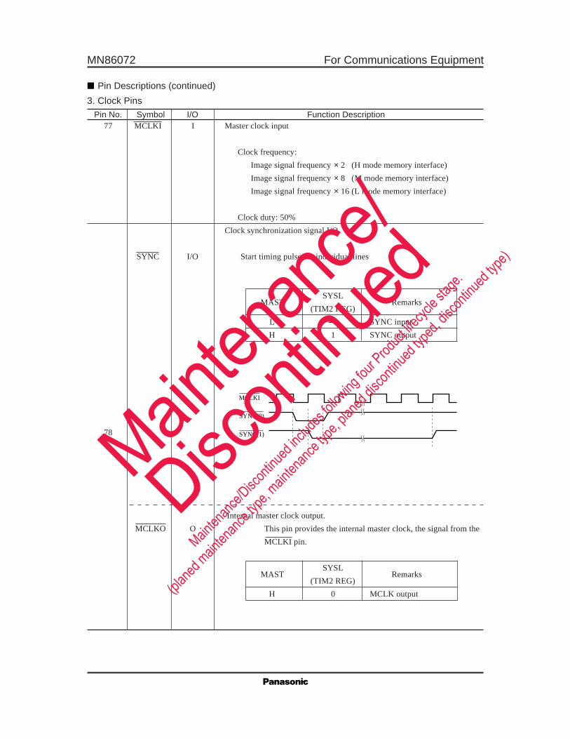
Internal master clock output.
MCLKO O This pin provides the internal master clock, the signal from the
MCLKI pin.
MASTSYSL
Remarks(TIM2 REG)
H 0 MCLK output
77 MCLKI I Master clock input
Clock frequency:
Image signal frequency × 2 (H mode memory interface)
Image signal frequency × 8 (M mode memory interface)
Image signal frequency × 16 (L mode memory interface)
Clock duty: 50%
Clock synchronization signal I/O
SYNC I/O Start timing pulse for individual lines
MASTSYSL
Remarks(TIM2 REG)
L — SYNC input
H 1 SYNC output
3. Clock Pins
Pin No. Symbol I/O Function Description
Pin Descriptions (continued)
78
MCLKI
SYNC(0)
SYNC(1)Mainten
ance/
Discon
tinued
Mainten
ance/D
iscont
inued
includ
es foll
owing
four P
roduct
lifecyc
le stag
e.
(planed
mainten
ance ty
pe, main
tenanc
e type,
planed
discon
tinued
typed,
discon
tinued
type)
For Communications Equipment MN86072
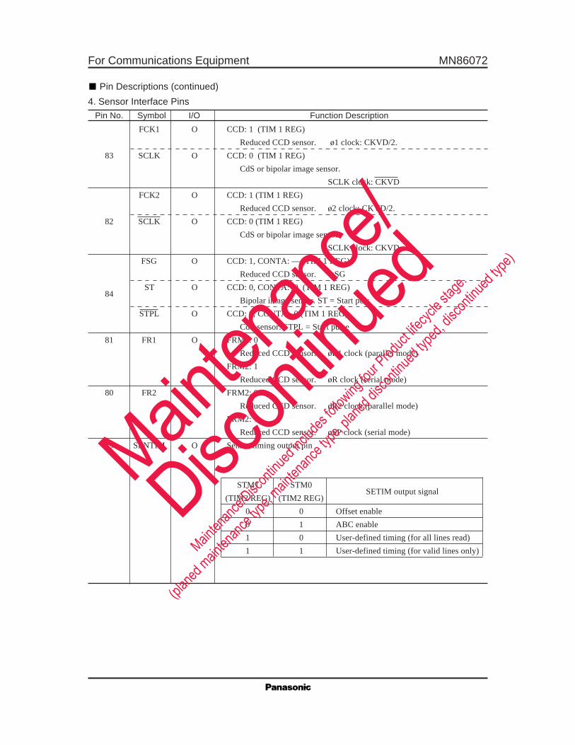
FCK1 O CCD: 1 (TIM 1 REG)
Reduced CCD sensor. ø1 clock: CKVD/2.
83 SCLK O CCD: 0 (TIM 1 REG)
CdS or bipolar image sensor.
SCLK clock: CKVD
FCK2 O CCD: 1 (TIM 1 REG)
82
Reduced CCD sensor. ø2 clock: CKVD/2.
SCLK O CCD: 0 (TIM 1 REG)
CdS or bipolar image sensor.
SCLK clock: CKVD
FSG O CCD: 1, CONTA: — (TIM 1 REG)
Reduced CCD sensor. øSG
84ST O CCD: 0, CONTA: 0 (TIM 1 REG)
Bipolar image sensor. ST = Start puls
STPL O CCD: 0, CONTA: 0 (TIM 1 REG)
CdS sensor. STPL = Start pulse
81 FR1 O FRM2: 0
Reduced CCD sensor. øR1 clock (parallel mode)
FRM2: 1
Reduced CCD sensor. øR clock (serial mode)
80 FR2 O FRM2: 0
Reduced CCD sensor. øR2 clock (parallel mode)
FRM2: 1
Reduced CCD sensor. øSP clock (serial mode)
79 SENTIM O Sensor timing output pin
STM1 STM0SETIM output signal
(TIM2 REG) (TIM2 REG)
0 0 Offset enable
0 1 ABC enable
1 0 User-defined timing (for all lines read)
1 1 User-defined timing (for valid lines only)
4. Sensor Interface Pins
Pin No. Symbol I/O Function Description
Pin Descriptions (continued)
Mainten
ance/
Discon
tinued
Mainten
ance/D
iscont
inued
includ
es foll
owing
four P
roduct
lifecyc
le stag
e.
(planed
mainten
ance ty
pe, main
tenanc
e type,
planed
discon
tinued
typed,
discon
tinued
type)

MN86072 For Communications Equipment
44 PEAK1 O Gain control signal 1 (Overflow 1)
"L" level: Reduce gain.
"H" level: Increase gain.
43 PEAK2 O Gain control signal 2 (Overflow 2)
"L" level: Reduce gain.
"H" level: Increase gain.
45 CLAMP O Clamp (offset correction) interval signal.
"L" level: Hold.
"H" level: Sample (offset adjustment operation).
46 ABC O ABC effective interval signal.
"L" level: Hold gain.
"H" level: Adjust gain.
5. Sensor Drive PinsPin No. Symbol I/O Function Description
Pin Descriptions (continued)
Mainten
ance/
Discon
tinued
Mainten
ance/D
iscont
inued
includ
es foll
owing
four P
roduct
lifecyc
le stag
e.
(planed
mainten
ance ty
pe, main
tenanc
e type,
planed
discon
tinued
typed,
discon
tinued
type)

For Communications Equipment MN86072
47 VREQ I Video request.
This pin accepts image data transfer requests from the controlled device.
"L" level: Transfer request enable.
"H" level: Transfer request disable.
In the trigger scan mode, pulling this pin to "L" level forces the
sensor start (STPL) pin to "L" level to start sensor readout. After
image-processing a line of data, the image data are outputted at
the VSDA pin.
In the cycle scan mode, pulling this pin to "L" level enables the next
readout line. After image-processing a line of data, the image data
are outputted at the VSDA pin.
In the free scan mode, the chip ignores this pin, sensor readout starts
at the interval specified with the timing settings, and the image data
are outputted at the VSDA pin after processing each line of data.
Parallel mode (IPARA (IBCNT REGI): 1)
DREQ O Parallel data transfer request.
"L" level: Transfer request enable.
49"H" level: Transfer request disable.
Serial mode (IPARA (IBCNT REGI): 0)
VSEN O Video enable
"L" level: Image data enable.
"H" level: Image data disable.
48 DACK I Parallel data acknowledge.
Data transfer acknowledge signal in response to DREQ.
"L" level: Data transfer enable.
"H" level: Data transfer disable.
6. Image Bus Interface PinsPin No. Symbol I/O Function Description
Pin Descriptions (continued)
Mainten
ance/
Discon
tinued
Mainten
ance/D
iscont
inued
includ
es foll
owing
four P
roduct
lifecyc
le stag
e.
(planed
mainten
ance ty
pe, main
tenanc
e type,
planed
discon
tinued
typed,
discon
tinued
type)
MN86072 For Communications Equipment
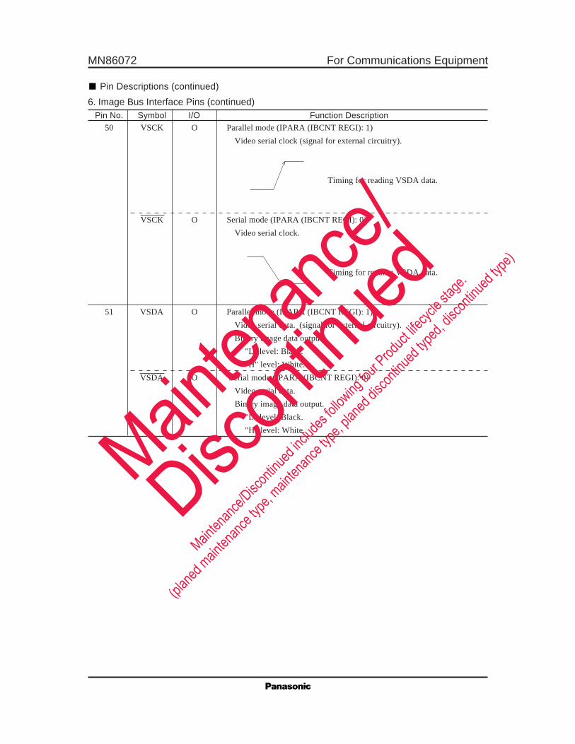
50 VSCK O Parallel mode (IPARA (IBCNT REGI): 1)
Video serial clock (signal for external circuitry).
Timing for reading VSDA data.
VSCK O Serial mode (IPARA (IBCNT REGI): 0)
Video serial clock.
Timing for reading VSDA data.
51 VSDA O Parallel mode (IPARA (IBCNT REGI): 1)
Video serial data. (signal for external circuitry).
Binary image data output.
"L" level: Black.
"H" level: White.
VSDA O Serial mode (IPARA (IBCNT REGI): 0)
Video serial data.
Binary image data output.
"L" level: Black.
"H" level: White.
6. Image Bus Interface Pins (continued)Pin No. Symbol I/O Function Description
Pin Descriptions (continued)
Mainten
ance/
Discon
tinued
Mainten
ance/D
iscont
inued
includ
es foll
owing
four P
roduct
lifecyc
le stag
e.
(planed
mainten
ance ty
pe, main
tenanc
e type,
planed
discon
tinued
typed,
discon
tinued
type)
For Communications Equipment MN86072
7. Parallel I/O Pins
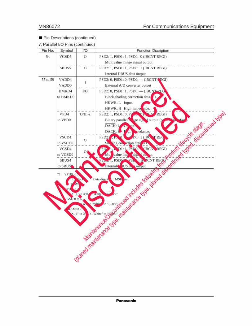
Pin No. Symbol I/O Function Description
Pin Descriptions (continued)
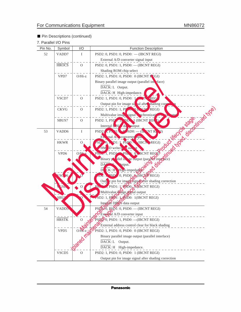
52 VADD7 I PSD2: 0, PSD1: 0, PSD0: — (IBCNT REGI)
External A/D converter signal input
HROCS O PSD2: 0, PSD1: 1, PSD0: — (IBCNT REGI)
Shading ROM chip select
VPD7 O/Hi-z PSD2: 1, PSD1: 0, PSD0: 0 (IBCNT REGI)
Binary parallel image output (parallel interface)
DACK: L Output.
DACK: H High-impedance.
VSCD7 O PSD2: 1, PSD1: 0, PSD0: 1 (IBCNT REGI)
Output pin for image signal after shading correction
CKVG O PSD2: 1, PSD1: 1, PSD0: 0 (IBCNT REGI)
Multivalue image signal synchronization clock output
SBUS7 O PSD2: 1, PSD1: 1, PSD0: 1 (IBCNT REGI)
Internal DBUS data output
53 VADD6 I PSD2: 0, PSD1: 0, PDSD0: — (IBCNT REGI)
External A/D converter input
HKWR O PSD2: 0, PSD1: 1, PSD0: — (IBCNT REGI)
HMKD write/read output
VPD6 O/Hi-z PSD2: 1, PSD1: 0, PSD0: 0 (IBCNT REGI)
Binary parallel image output (parallel interface)
DACK: L Output.
DACK: H High-impedance.
VSCD6 O PSD2: 1, PSD1: 0, PSD0: 1 (IBCNT REGI)
Output pin for image signal after shading correction
VGSD6 O PSD2: 1, PSD1: 1, PSD0: 0 (IBCNT REGI)
Multivalue image signal output
SBUS6 O PSD2: 1, PSD1: 1, PSD0: 1(IBCNT REGI)
Internal DBUS data output
54 VADD5 I PSD2: 0, PSD1: 0, PSD0: — (IBCNT REGI)
External A/D converter input
HRSTK O PSD2: 0, PSD1: 1, PSD0: —(IBCNT REGI)
External address control clear for black shading
VPD5 O/Hi-z PSD2: 1, PSD1: 0, PSD0: 0 (IBCNT REGI)
Binary parallel image output (parallel interface)
DACK: L Output.
DACK: H High-impedance.
VSCD5 O PSD2: 1, PSD1: 0, PSD0: 1 (IBCNT REGI)
Output pin for image signal after shading correction
Mainten
ance/
Discon
tinued
Mainten
ance/D
iscont
inued
includ
es foll
owing
four P
roduct
lifecyc
le stag
e.
(planed
mainten
ance ty
pe, main
tenanc
e type,
planed
discon
tinued
typed,
discon
tinued
type)
MN86072 For Communications Equipment
7. Parallel I/O Pins (continued)
Pin No. Symbol I/O Function Dscription
Pin Descriptions (continued)
54 VGSD5 O PSD2: 1, PSD1: 1, PSD0: 0 (IBCNT REGI)
Multivalue image signal output
SBUS5 O PSD2: 1, PSD1: 1, PSD0: 1 (IBCNT REGI)
Internal DBUS data output
55 to 59 VADD4I
PSD2: 0, PSD1: 0, PSD0: — (IBCNT REGI)
VADD0 External A/D converter output
HMKD4 I/O PSD2: 0, PSD1: 1, PSD0: — (IBCNT REGI)
to HMKD0 Black shading correction data I/O.
HKWR: L Input.
HKWR: H High-impedance.
VPD4 O/Hi-z PSD2: 1, PSD1: 0, PSD0: 0 (IBCNT REGI)
to VPD0 Binary parallel image signal output (parallel interface)
DACK: L Output.
DACK: H High-impedance.
VSCD4O
PSD2: 1, PSD1: 0, PSD0: 1 (IBCNT REGI)
to VSCD0 Shading correction data I/O.
VGSD4O
PSD2: 1, PSD1: 1, PSD0: 0 (IBCNT REGI)
to VGSD0 Multivalue image signal output
SBUS4O
PSD2: 1, PSD1: 1, PSD0: 1(IBCNT REGI)
to SBUS0 Internal DBUS data output
*1 VPD0 to 7
1: Black Data direction: MSB first
0: White
*2 VPD0 to 7
X'FF' to X'00': "White" to "Black"
*3 VGSD 0 to 6
X'7F' to X'00': "White" to "Black"
*4 VADD0 to 7
X'FF' to X'00': "White" to "Black"Main
tenan
ce/
Discon
tinued
Mainten
ance/D
iscont
inued
includ
es foll
owing
four P
roduct
lifecyc
le stag
e.
(planed
mainten
ance ty
pe, main
tenanc
e type,
planed
discon
tinued
typed,
discon
tinued
type)
For Communications Equipment MN86072
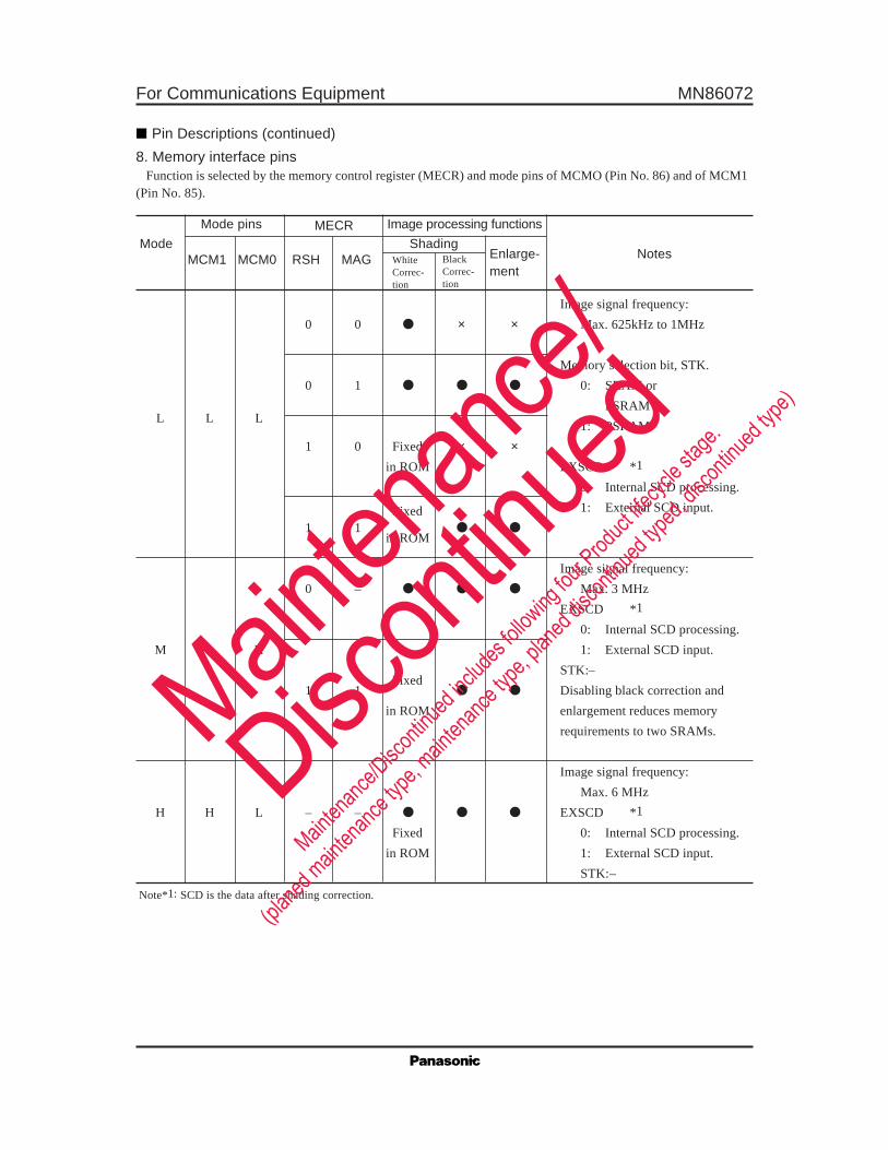
Image signal frequency:
0 0 ● × × Max. 625kHz to 1MHz
Memory selection bit, STK.
L L L
0 1 ● ● ● 0: SRAM or
PSRAM
1: PSRAM
1 0 Fixed × ×in ROM EXSCD *1
0: Internal SCD processing.
Fixed 1: External SCD input.
1 1in ROM
● ●
Image signal frequency:
0 – ● ● ● Max. 3 MHz
EXSCD *1
0: Internal SCD processing.
M L H 1: External SCD input.
FixedSTK:–
1 1 ● ● Disabling black correction and
in ROM enlargement reduces memory
requirements to two SRAMs.
Image signal frequency:
Max. 6 MHz
H H L – – ● ● ● EXSCD *1
Fixed 0: Internal SCD processing.
in ROM 1: External SCD input.
STK:–
8. Memory interface pins
Pin Descriptions (continued)
Function is selected by the memory control register (MECR) and mode pins of MCMO (Pin No. 86) and of MCM1(Pin No. 85).
Mode pins MECR Image processing functions
Mode MCM1 MCM0 RSH MAG
ShadingEnlarge- Notesment
WhiteCorrec-tion
BlackCorrec-tion
Note*1: SCD is the data after shading correction.
Mainten
ance/
Discon
tinued
Mainten
ance/D
iscont
inued
includ
es foll
owing
four P
roduct
lifecyc
le stag
e.
(planed
mainten
ance ty
pe, main
tenanc
e type,
planed
discon
tinued
typed,
discon
tinued
type)
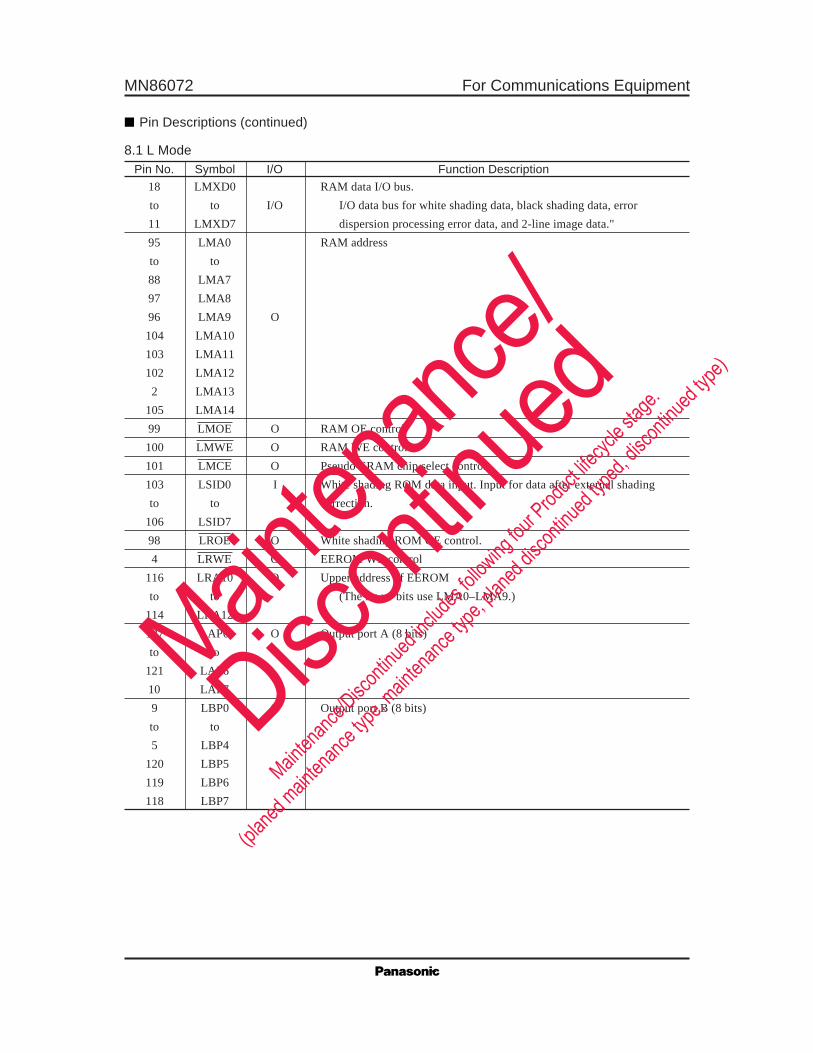
MN86072 For Communications Equipment
18 LMXD0 RAM data I/O bus.
to to I/O I/O data bus for white shading data, black shading data, error
11 LMXD7 dispersion processing error data, and 2-line image data."
95 LMA0 RAM address
to to
88 LMA7
97 LMA8
96 LMA9 O
104 LMA10
103 LMA11
102 LMA12
2 LMA13
105 LMA14
99 LMOE O RAM OE control
100 LMWE O RAM WE control
101 LMCE O Pseudo-SRAM chip select control
103 LSID0 I White shading ROM data input. Input for data after external shading
to to correction.
106 LSID7
98 LROE O White shading ROM OE control.
4 LRWE O EEROM WE control
116 LRA10 O Upper address of EEROM
to to (The lower bits use LMA0–LMA9.)
114 LRA12
127 LAP0 O Output port A (8 bits)
to to
121 LAP6
10 LAP7
9 LBP0 O Output port B (8 bits)
to to
5 LBP4
120 LBP5
119 LBP6
118 LBP7
8.1 L ModePin No. Symbol I/O Function Description
Pin Descriptions (continued)
Mainten
ance/
Discon
tinued
Mainten
ance/D
iscont
inued
includ
es foll
owing
four P
roduct
lifecyc
le stag
e.
(planed
mainten
ance ty
pe, main
tenanc
e type,
planed
discon
tinued
typed,
discon
tinued
type)
For Communications Equipment MN86072
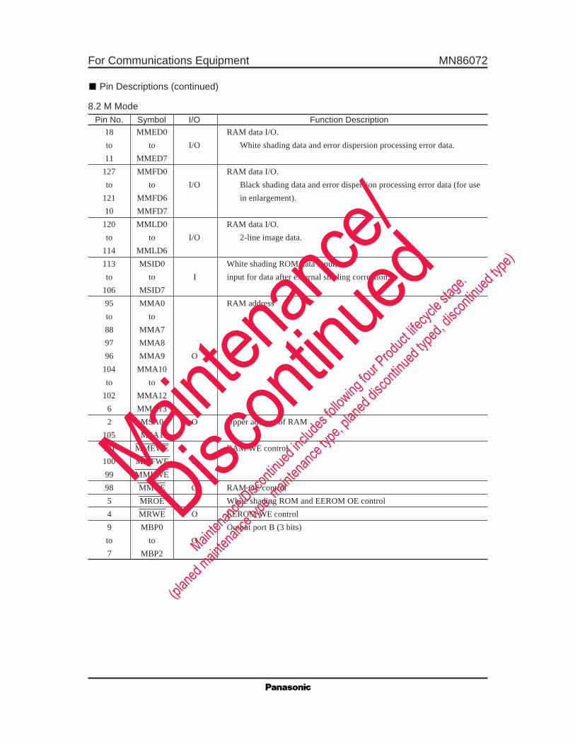
18 MMED0 RAM data I/O.
to to I/O White shading data and error dispersion processing error data.
11 MMED7
127 MMFD0 RAM data I/O.
to to I/O Black shading data and error dispersion processing error data (for use
121 MMFD6 in enlargement).
10 MMFD7
120 MMLD0 RAM data I/O.
to to I/O 2-line image data.
114 MMLD6
113 MSID0 White shading ROM data input, or
to to I input for data after external shading correction.
106 MSID7
95 MMA0 RAM address
to to
88 MMA7
97 MMA8
96 MMA9 O
104 MMA10
to to
102 MMA12
6 MMA13
2 MSA0 O Upper address of RAM
105 MSA1
101 MMEWE RAM WE control
100 MMFWE O
99 MMLWE
98 MMOE O RAM OE control
5 MROE O White shading ROM and EEROM OE control
4 MRWE O EEROM WE control
9 MBP0 Output port B (3 bits)
to to O
7 MBP2
8.2 M ModePin No. Symbol I/O Function Description
Pin Descriptions (continued)
Mainten
ance/
Discon
tinued
Mainten
ance/D
iscont
inued
includ
es foll
owing
four P
roduct
lifecyc
le stag
e.
(planed
mainten
ance ty
pe, main
tenanc
e type,
planed
discon
tinued
typed,
discon
tinued
type)
MN86072 For Communications Equipment
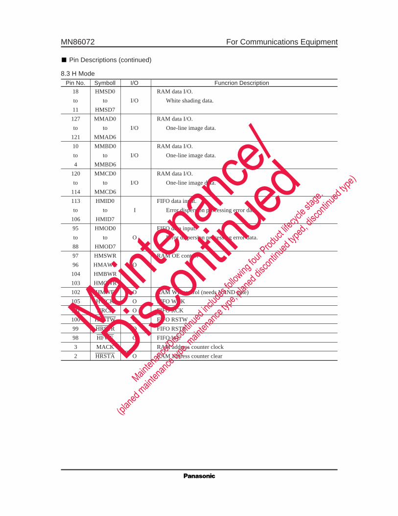
18 HMSD0 RAM data I/O.
to to I/O White shading data.
11 HMSD7
127 MMAD0 RAM data I/O.
to to I/O One-line image data.
121 MMAD6
10 MMBD0 RAM data I/O.
to to I/O One-line image data.
4 MMBD6
120 MMCD0 RAM data I/O.
to to I/O One-line image data.
114 MMCD6
113 HMID0 FIFO data input.
to to I Error dispersion processing error data.
106 HMID7
95 HMOD0 FIFO data input.
to to O Error dispersion processing error data.
88 HMOD7
97 HMSWR RAM OE control
96 HMAWR O
104 HMBWR
103 HMCWR
102 HMWE O RAM WE control (needs NAND gate)
105 HWCK O FIFO WCK
101 HRCK O FIFO RCK
100 HRSTW O FIFO RSTW
99 HRSTR O FIFO RSTR
98 HFWE O FIFO WE
3 MACK O RAM address counter clock
2 HRSTA O RAM address counter clear
8.3 H ModePin No. Symboll I/O Funcrion Description
Pin Descriptions (continued)
Mainten
ance/
Discon
tinued
Mainten
ance/D
iscont
inued
includ
es foll
owing
four P
roduct
lifecyc
le stag
e.
(planed
mainten
ance ty
pe, main
tenanc
e type,
planed
discon
tinued
typed,
discon
tinued
type)
For Communications Equipment MN86072
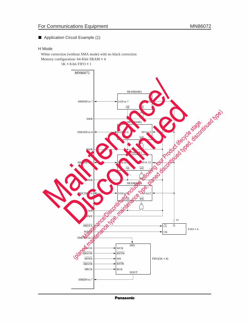
Application Circuit Example (1)
H ModeWhite correction (without SMA mode) with no black correctionMemory configuration: 64-Kbit SRAM × 4
5K × 8-bit FIFO × 1
SRAM(64K)
SRAM(64K)
I/O0 to 7 A0 to 12
OE WE
I/O0 to 6 A0 to 12
OE
OE
WE
SRAM(64K)
SRAM(64K)
I/O0 to 6
I/O0 to 6
A0 to 12
A0 to12
WE
OE WE
13
CL
CK
QF163 × 4
DINWCK
RSTW
WE
RSTR
RCKDOUT
FIFO(5K × 8)
MN86072
HMSD0 to 7
SWR
HMAD0 to 6
HMBD0 to 6
BWR
HMCD0 to 6
CWR
HMWE
HRSTA
HMOD0 to 7
MACK
HWCK
HRSTW
HRCK
HMID0 to 7
AWR
HRSTR
HFWE
Mainten
ance/
Discon
tinued
Mainten
ance/D
iscont
inued
includ
es foll
owing
four P
roduct
lifecyc
le stag
e.
(planed
mainten
ance ty
pe, main
tenanc
e type,
planed
discon
tinued
typed,
discon
tinued
type)
MN86072 For Communications Equipment
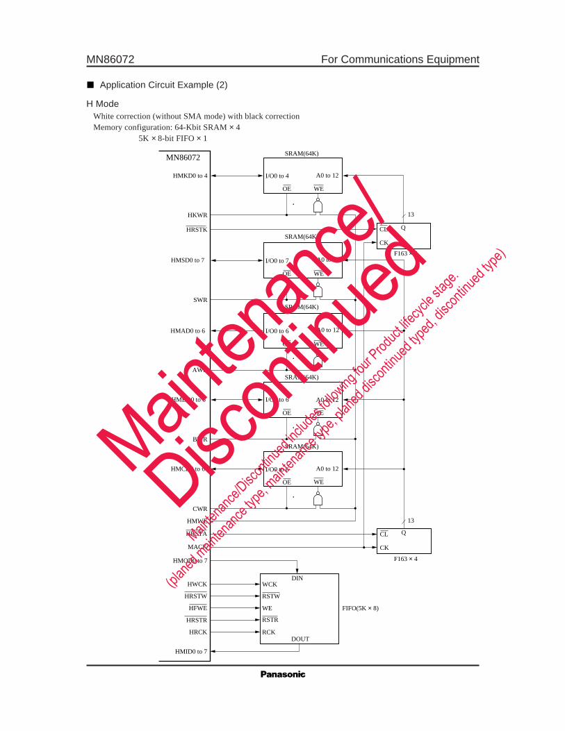
Application Circuit Example (2)
H ModeWhite correction (without SMA mode) with black correctionMemory configuration: 64-Kbit SRAM × 4
5K × 8-bit FIFO × 1
SRAM(64K)
SRAM(64K)
I/O0 to 4 A0 to 12
OE WE
I/O0 to 6 A0 to 12
OE
OE
WE
SRAM(64K)
I/O0 to 7 A0 to 12
OE WE
SRAM(64K)
SRAM(64K)
I/O0 to 6
I/O0 to 6
A0 to 12
A0 to 12
WE
OE WE
13
13
CL
CK
Q
F163 × 4
CL
CK
Q
F163 × 4
DINWCK
RSTW
WE
RSTR
RCKDOUT
FIFO(5K × 8)
MN86072
HMKD0 to 4
HMSD0 to 7
SWR
HKWR
HRSTK
HMAD0 to 6
HMBD0 to 6
BWR
HMCD0 to 6
CWR
HMWE
HRSTA
HMOD0 to 7
MACK
HWCK
HRSTW
HRCK
HMID0 to 7
AWR
HRSTR
HFWE
Mainten
ance/
Discon
tinued
Mainten
ance/D
iscont
inued
includ
es foll
owing
four P
roduct
lifecyc
le stag
e.
(planed
mainten
ance ty
pe, main
tenanc
e type,
planed
discon
tinued
typed,
discon
tinued
type)
For Communications Equipment MN86072
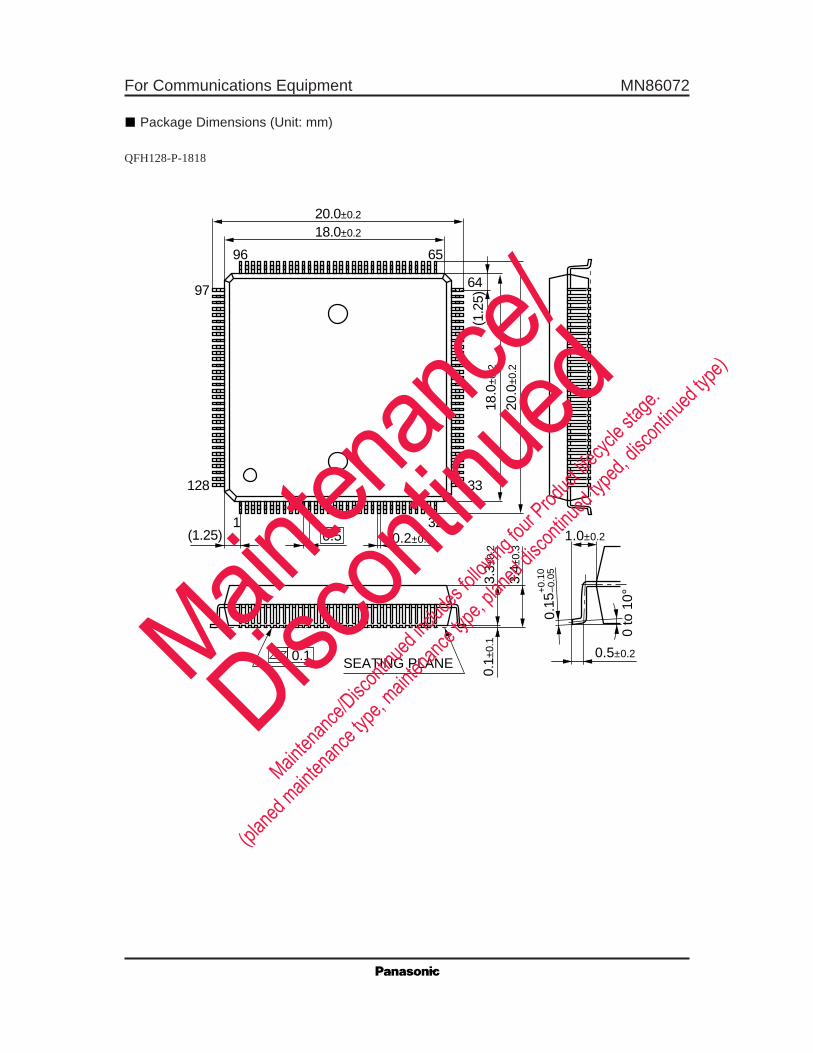
Package Dimensions (Unit: mm)
QFH128-P-1818
0.2±0.1
0.5±0.2
(1.25)
(1.2
5)33128
97
18.0±0.2
18.0
±0.2
0.1±
0.1
20.0
±0.2
20.0±0.2
0 to
10°
1.0±0.2
64
3.4±
0.3
3.3±
0.2
96 65
1 320.5
0.1 SEATING PLANE
0.15
+0.
10–0
.05
Mainten
ance/
Discon
tinued
Mainten
ance/D
iscont
inued
includ
es foll
owing
four P
roduct
lifecyc
le stag
e.
(planed
mainten
ance ty
pe, main
tenanc
e type,
planed
discon
tinued
typed,
discon
tinued
type)

Request for your special attention and precautions in using the technical information andsemiconductors described in this book
(1)If any of the products or technical information described in this book is to be exported or provided to non-residents, the laws and regulations of the exporting country, especially, those with regard to security export control, must be observed.
(2)The technical information described in this book is intended only to show the main characteristics and application circuit examples of the products, and no license is granted under any intellectual property right or other right owned by our company or any other company. Therefore, no responsibility is assumed by our company as to the infringement upon any such right owned by any other company which may arise as a result of the use of technical information described in this book.
(3)The products described in this book are intended to be used for standard applications or general electronic equipment (such as office equipment, communications equipment, measuring instruments and household appliances). Consult our sales staff in advance for information on the following applications:� Special applications (such as for airplanes, aerospace, automobiles, traffic control equipment, combustion equipment, life support
systems and safety devices) in which exceptional quality and reliability are required, or if the failure or malfunction of the prod-ucts may directly jeopardize life or harm the human body.� Any applications other than the standard applications intended.
(4)The products and product specifications described in this book are subject to change without notice for modification and/or im-provement. At the final stage of your design, purchasing, or use of the products, therefore, ask for the most up-to-date Product Standards in advance to make sure that the latest specifications satisfy your requirements.
(5)When designing your equipment, comply with the range of absolute maximum rating and the guaranteed operating conditions (operating power supply voltage and operating environment etc.). Especially, please be careful not to exceed the range of absolute maximum rating on the transient state, such as power-on, power-off and mode-switching. Otherwise, we will not be liable for any defect which may arise later in your equipment.
Even when the products are used within the guaranteed values, take into the consideration of incidence of break down and failure mode, possible to occur to semiconductor products. Measures on the systems such as redundant design, arresting the spread of fire or preventing glitch are recommended in order to prevent physical injury, fire, social damages, for example, by using the products.
(6)Comply with the instructions for use in order to prevent breakdown and characteristics change due to external factors (ESD, EOS, thermal stress and mechanical stress) at the time of handling, mounting or at customer's process. When using products for which damp-proof packing is required, satisfy the conditions, such as shelf life and the elapsed time since first opening the packages.
(7)This book may be not reprinted or reproduced whether wholly or partially, without the prior written permission of Matsushita Electric Industrial Co., Ltd.
Mainten
ance/
Discon
tinued
Mainten
ance/D
iscont
inued
includ
es foll
owing
four P
roduct
lifecyc
le stag
e.
(planed
mainten
ance ty
pe, main
tenanc
e type,
planed
discon
tinued
typed,
discon
tinued
type)