Embed Size (px)
Citation preview
FLUX PINNING IN SUPERCONDUCTING Nb-Ti WIRES
WITH Nb ARTIFICIAL PINNING CENTERS
by
Robert W. Heussner
A dissertation submitted in partial fulfillment
of the requirements for the degree of
Doctor of Philosophy
(Materials Science)
at the
UNIVERSITY OF WISCONSIN - MADISON
1998

© Copyright by Robert W. Heussner 1998All Rights Reserved

i
Acknowledgments
I thank my advisor, Professor David Larbalestier, for providing me with many
opportunities, encouragement, and guidance over the years for which I am truly grateful.
I also appreciate the help and friendship of the entire Superconducting Materials
Research Group, who made my time at UW enjoyable.
In particular, I thank: Paul Jablonski, for teaching me the fine art of composite wire
manufacture, and whose own work provided a basis for this thesis; Lance Cooley, for his
close collaboration throughout this work; Peter Lee, for performing painstaking TEM on
my wires; Cristina Bormio-Nunes, for providing electromagnetic characterization which
complemented my own experimental results; and Alex Pashitski, Alex Gurevich, Jeff
Parrell and Mike Naus, for helpful scientific discussions. I was also fortunate to work
with several bright undergraduates, including Jesse Marquardt, Matt Schlinkert, and
Matt Pelletier, who assisted in the fabrication and characterization of composite wires.
A special thanks is due to Bill Starch and Alex Squitieri who, in addition to
maintaining our excellent fabrication and electromagnetic characterization facilities, were
always willing to devote their time to this project. I also thank Mel Adams and Kim
Bass, who deserve much credit for keeping the Center running smoothly. I thank my
doctoral committee, particularly Professors Eric Hellstrom, Sue Babcock, Tom Kelly,
and David for their excellent instruction throughout my materials science education.

ii
Finally, I am indebted to my parents, Bob and Sarah, for their support in all the
choices I have made. I am forever grateful to my wife, Wendy, for her love and
encouragement.

iii
FLUX PINNING IN SUPERCONDUCTING Nb-Ti WIRES
WITH Nb ARTIFICIAL PINNING CENTERS
Robert W. Heussner
Under the supervision of Professor David C. Larbalestier
At the University of Wisconsin-Madison
Superconducting Nb-Ti wires containing uniform arrays of round Nb artificial pinning
centers were fabricated and their microstructures and electromagnetic properties
characterized as the pin diameter and spacing were reduced to the nanometer dimensions
of the flux line lattice. Through careful control of the thermomechanical treatment, the
critical current density (Jc) of a composite containing Nb 47 wt.% Ti with 24 volume
percent of Nb pins was raised to 4600 A/mm2 at the benchmark field (5 T) and
temperature (4.2 K), thus establishing a new record for any round wire of Nb-Ti.
Maximum Jc(5 T) occurred for a nominal pin diameter (dp) of 25 nm, but for which the
actual pins were 1–15 nm thick elongated ribbons. Despite the extremely high Jc values
at low fields (1–6 T), the high-field Jc (6–9 T) was depressed due to the combination of a
proximity-effect depressed upper critical field, and a characteristic low-field maximum in
the field-dependent pinning force density. A Nb 62 wt.% Ti-matrix composite, designed
for maximum upper critical field in the coupled limit, exhibited an increased irreversibility
field as the pin size was reduced. However, this enhancement was significantly less than

iv
predicted for the fully coupled limit, even when the pins were much thinner than the
superconducting coherence length. In the context of existing proximity effect models,
this can be attributed to the same minimal pin/matrix interdiffusion held responsible for
high Jc at low fields. Finally, through separate alloying additions of 7.5 wt.% Ta and 10
wt.% W, the Nb-pin proximity length (ξN) was reduced by 30% and 60%, respectively.
The functional dependence of the pinning force density on ξN, dp, and field agrees
qualitatively with the magnetic pinning model of Cooley, Lee, and Larbalestier.

v
Contents
Abstract ..................................................................................................................... iii
1. Introduction.............................................................................................................1
1.1 Flux pinning in type-II superconductors ............................................................2
1.1.1 Elementary pinning force.........................................................................4
1.1.2 Bulk pinning force...................................................................................7
1.2 Development of high-Jc Nb-Ti wire.................................................................10
1.3 Artificial pinning center wire ...........................................................................12
1.3.1 Proximity-effect depression of Tc, Hc2....................................................15
1.3.2 The shape of Fp(H) ...............................................................................17
1.4 Design of this thesis ........................................................................................18
2. APC wire design, fabrication, and characterization ............................................23
2.1 Wire Design....................................................................................................25
2.1.1 Pinning array design ..............................................................................25
2.1.2 Selection of pin material, pin fraction, and matrix composition ..............26
2.1.3 Process design.......................................................................................27
2.2 Wire fabrication ..............................................................................................29
2.2.1 Composite billet design .........................................................................29
2.2.2 Composite billet assembly .....................................................................30
2.2.3 Extrusion ..............................................................................................32
2.2.4 Wire drawing and re-stacking................................................................36
2.2.5 Reduction of copper-to-superconductor ratio ........................................37
2.2.6 Multifilament wires ...............................................................................38
2.3 Characterization techniques.............................................................................39
vi
2.3.1 Transport Jc measurements................................................................... 39
2.3.2 Magnetization measurements................................................................ 40
3. Properties of Nb-Ti wires with Nb artificial pinning centers .............................. 43
3.1 Experimental Design ...................................................................................... 44
3.2 Results ........................................................................................................... 48
3.3 Discussion...................................................................................................... 53
3.3.1 Microstructure ..................................................................................... 53
3.3.2 Jc vs. dp ................................................................................................ 55
3.3.3 Fp(H) curve shapes............................................................................... 57
3.3.4 H* vs. dp .............................................................................................. 58
3.3.5 An effective comparison procedure for conventional and APC wires..... 59
3.4 Conclusions.................................................................................................... 61
4. Improved thermomechanical processing ............................................................. 63
4.1 Experimental design ....................................................................................... 65
4.2 Results ........................................................................................................... 67
4.3 Discussion...................................................................................................... 69
4.4 Conclusions.................................................................................................... 75
5. Effect of Nb-Ti matrix composition...................................................................... 77
5.1 Experimental design ....................................................................................... 78
5.2 Results ........................................................................................................... 80
5.3 Discussion...................................................................................................... 86
5.3.1 Microstructural development ................................................................ 86
5.3.2 H* and Hc2 vs. dp.................................................................................. 87
5.3.3 Proximity effect theory ......................................................................... 89
5.4 Conclusions.................................................................................................... 91

vii
6. Effect of pin proximity length ...............................................................................93
6.1 Experimental design........................................................................................95
6.2 Results............................................................................................................98
6.3 Discussion ....................................................................................................103
6.4 Conclusions ..................................................................................................106
7. Summary............................................................................................................107
Bibliography ............................................................................................................108

viii
1
1. Introduction
Niobium titanium is the most widely used superconductor. This is despite the existence
of other superconductors which possess higher critical temperatures ( Tc ) and critical
magnetic fields, most notably the A15 (e.g. Nb3Sn), Chevrel phase (e.g. PbMo6S8) and
high-temperature copper-oxide (e.g. Bi2Sr2CaCu2O8 and YBa2Cu3O7) ceramic
compounds. Nb-Ti is chosen because it is ductile, strong, and provides a technologically
useful critical current density (Jc>1 kA/mm2) in fields up to ~8 T at 4.2 K and ~11 T at
1.8 K. High energy physics projects propel the investigation of ever greater high-field Jc
in Nb-Ti since particle accelerator magnets benefit from high Jc. Furthermore, mature
technologies such as magnetic resonance imaging, electric power conditioning, and
laboratory magnets benefit from all Jc improvements. In bulk superconducting materials,
Jc can be determined by a hierarchy of limiting mechanisms, but it is ultimately limited by
the pinning of the flux line lattice by the defect structure. Thus the key to raising Jc lies

2
in controlling the defect structure and relating it to the flux pinning and other
superconducting properties.
1.1 Flux pinning in type-II superconductors
Two distinct types of superconductors are characterized by their response to applied
magnetic fields, as illustrated by the H–T phase diagrams of Figure 1.1. To understand
the origin of the difference in behavior requires a microscopic description of the
superconducting properties. All superconductors are characterized by two intrinsic
length scales: the magnetic penetration depth (λ) [1], or the distance over which the
magnetic field (H) can vary, and the coherence length (ξ) [2], or the distance over which
the superconducting order parameter (Ψ) can vary. The ratio of these two lengths,
called the Ginzburg-Landau parameter (κ) [3],
κ λ ξ= , (1.1)
determines whether the superconductor is type-I or type-II. Type-I superconductors
(κ < 1 2/ ) have a positive interfacial energy between the normal and superconducting
states, given approximately by ( )12 0
2µ ξ λH c − [4]. Thus complete flux exclusion, or a
so-called Meissner state, [5] minimizes the interface energy. This state persists up to the
critical field (Hc) of order 10–100 mT. At this point, the further increase in free energy
due to flux exclusion exceeds the decrease in free energy associated with the
superconducting state and the material returns to the normal state.

3
Conversely, type-II superconductors (κ > 1 2/ ) have a negative normal–
superconductor interfacial energy and thus flux inclusion becomes energetically favorable
above a lower critical field (Hc1). In order to maximize the contribution of interface
energy, flux penetrates the superconductor in many discrete flux quanta or fluxons, each
fluxon containing a single flux quantum (φ0) given by:
φ 0152 2 07 10= = × −h e . Wb . (1.2)
The structure of a fluxon structure consists of a short-range (of order ξ) normal core
surrounded by a long-range (of order λ) vortex of supercurrent. As the field is increased
further beyond Hc1, the density of fluxons increases, and fluxon–fluxon repulsion leads to
Hc2( T)
Hc( T)
Hc1( T)
Tc
B=0(Meissner State)
Tc
N o rm al State
N o rm al State
H
T T
H
B=0(Mixed State)
B=0(Meissner State)
Figure 1.1: Schematic H–T phase diagrams for (a) type-I and (b) type-IIsuperconductors.

4
the formation of a hexagonal flux line lattice (FLL) with spacing a B0 0107= . φ [6].
Eventually, the internal flux density (B) equals the applied flux density at the upper
critical field (Hc2) defined by
H T H T Tc c2 0 022 2( ) ( ) ( )= =κ φ πµ ξ . (1.3)
The region of the H–T phase diagram between Hc1 and Hc2 (Figure 1.1b) is referred to as
the mixed (or vortex) state. All technologically useful superconducting materials are
type II because current is carried throughout the bulk and because the upper critical field
is much higher (of order T versus mT) than type I. Therefore, the remainder of this
chapter focuses on fluxon–defect and fluxon–fluxon interactions in type-II
superconductors.
1.1.1 Elementary pinning force
In the presence of a transport current density (J), the FLL of a type-II superconductor in
the mixed state experiences a bulk Lorentz force F J BL = × . A schematic of this
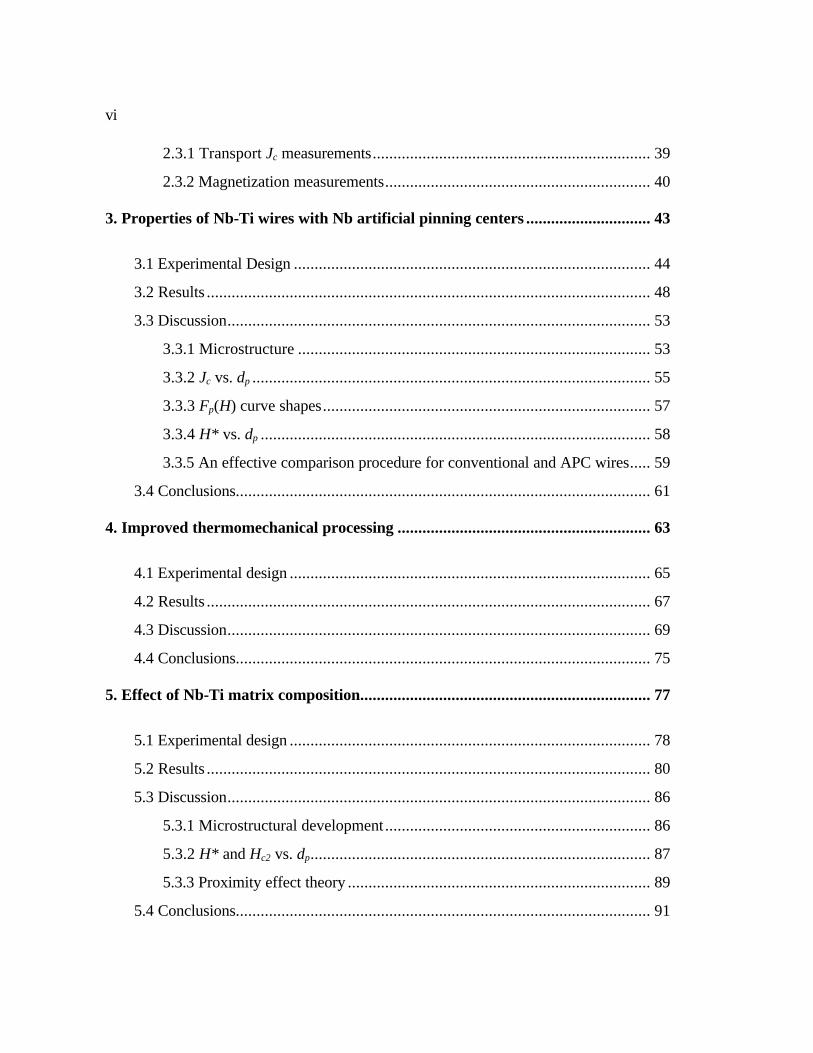
situation is shown in Figure 1.2 for a slab of type-II superconductor If left unbalanced,
the Lorentz force will move the fluxon cores, leading to energy dissipation and electrical
resistance. However, fluxons are easily pinned by regions of weaker superconductivity,
such as a microstructural defects. A vector sum of these elementary pinning forces (fp)
balances the Lorentz force.
5
Several mechanisms can give rise to an elementary pinning force. The normal core of
a fluxon is associated with a condensation energy density of order µ0Hc2 [7]. If the core
is located on a defect where the superconducting order parameter is locally depressed,
some or all of the condensation energy can be recovered. This is referred to as the core
interaction. For the simplest case of an isolated fluxon located over a void of diameter <
ξ, the energy penalty of the core is reduced by 12 0
2µ H Vc , where V is the volume of the
void. Dividing this energy by the characteristic distance over which Ψ varies gives a
rough estimate of the elementary pinning interaction:
f V Hp c= ( )2 02ξ µ . (1.4)
At finite reduced fields (h≡H/Hc2), the superconducting order parameter is reduced by a
factor of (1−h), yielding a field-dependent elementary pinning force:
J J
H
FL Fp
Figure 1.2: Force balance between the bulk pinning force Fp and the Lorentz force FL
which defines the critical state and Jc. The orientations of J, H, FL, and Fp are shown fora slab geometry.

6
f h V H hp c( ) ( ) ( )= −2 102ξ µ . (1.5)
However, voids are not practical pinning centers; non-superconducting precipitates are
usually encountered in practice. Kramer and Freyhardt [8] calculated the elementary
pinning force of a small (~ξ) proximity-effect coupled precipitate to be several orders of
magnitude lower than for a void of similar size. However, Matsushita [9] argued that
this analysis incorrectly treated the precipitate as a weak superconductor. Through
application of the phenomenological Ginzburg–Landau theory, Matsushita found that fp
of a coupled pin was approximately the same as that for a void. In support of this
theory, measurements of the specific pinning force (average elementary pinning force)
for normal-state α-Ti precipitates in conventionally processed Nb-Ti [10] were within a
factor of 3 of the theory, with suitable allowance for the shape of the precipitate. In
addition, flux pinning calculations by Stejic [11] for a simulated Nb-Ti microstructure
support the hypothesis of Matsushita.
In addition to core pinning, long-range distortion of the vortex supercurrent by
defects produces a magnetic pinning interaction. The magnetic pinning force can be
calculated by determining the vortex current configuration in the London approximation
[7, 12, 13]. Since the energy associated with the supercurrent is of the same order of
magnitude as the condensation energy associated with the core, magnetic pinning
interactions can be as strong as core pinning interactions.

7
1.1.2 Bulk pinning force
Equations such as 1.5 can be used to determine the strength of the interaction between a
single fluxon and a single pinning center. However, since Jc is determined by the bulk
pinning force rather than by any single elementary pinning interaction, the process by
which the elementary pinning forces are vectorially summed is very important.
Microscopically, the bulk pinning force (Fp) is determined by summation of the
elementary pinning forces over the number density of pinning interactions (N):
r rF f f Np i pi
i
N
p= ≈=
∑ η η1
. (1.6)
A pinning efficiency factor η [14] is introduced to account for the geometrical
distribution of pinning centers and the rigidity of the FLL. If the FLL interaction is
strong with respect to fp, then η → 0 and thus Fp → 0 . Conversely, if the FLL
interaction is much weaker than fp, then η is determined by a geometrical factor related
to the defect structure and Fp is determined by direct summation of the elementary
pinning forces. Direct summation implies that fp can be multiplied by N directly to give
the bulk pinning force; this is expected to be a reasonable approximation for a system of
strong pins with a spacing comparable to the FLL spacing. For core pinning,
F H h hp ( ) ( )∝ −1 as follows from Equation 1.3 and the expectation that N h∝ .
The derivation of Fp from microscopic quantities using Equation 1.6 requires a
thorough understanding of the pinning mechanism(s) and a quantitative description of
the defect structure. In most cases, neither of these are known with great certainty. The

8
force balance requires that Fp is determined by the product of the critical current density
and the flux density:
r r rF J Bp c= × . (1.7)
Note that when H>>Hc1, B~µ0H, so it is only necessary to know the applied field in
order to find Fp.
Temperature scaling of the field-dependent bulk pinning force in high-κ
superconductors (such as Nb-Ti) was first reported by Fietz and Webb [15] and can be
expressed as:
[ ]F H T f hp c
m= 2 ( ) ( ) , (1.8)
where m is the scaling exponent. Scaling of Fp(H) over a wide range of temperature is
usually a good indication that one pinning mechanism is present. Temperature scaling
has been observed in cold-worked Nb-Ti [10] and under certain conditions in optimized
Nb-Ti [10]. A lack of temperature scaling is usually attributed to the presence of more
than one type of pinning center or more than one type of pinning mechanism [7]. ( )f h
generally takes the form of h hp q( )1− , where the exponents p and q depend on both the
nature of the elementary pinning interaction and the elasticity of the flux line lattice [16].
Thus, measurements of the bulk pinning force as a function of field and temperature can
be used to deduce information about the pinning mechanism(s) that operate [7, 12].
9
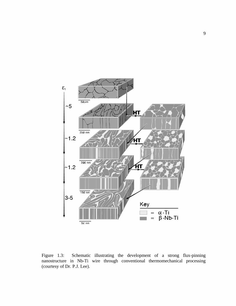
Figure 1.3: Schematic illustrating the development of a strong flux-pinningnanostructure in Nb-Ti wire through conventional thermomechanical processing(courtesy of Dr. P.J. Lee).
10
1.2 Development of high-Jc Nb-Ti wire
From the above discussion, an understanding of the flux pinning mechanism(s) in any
strong pinning system such as Nb-Ti is clearly desirable. However, the critical current
density in Nb-Ti was, in fact, optimized prior to the development of a generally accepted
flux pinning model. Jc optimization occurred primarily by means of microstructure–
property correlations—the principle tenet of materials science. Only after wires with
high-Jc were obtained (a situation corresponding to a high degree of both macro- and
microstructural uniformity), and then only after wire microstructures were quantitatively
characterized was a generally accepted flux-pinning model developed.
The key to increasing Jc in Nb-Ti via conventional thermomechanical treatment came
with the identification of non-superconducting α-Ti as the dominant, naturally occurring
defect [17]. Obtaining high Jc in Nb-Ti wire then became a matter of maximizing the
precipitate volume fraction and refining the precipitate size and spacing to dimensions
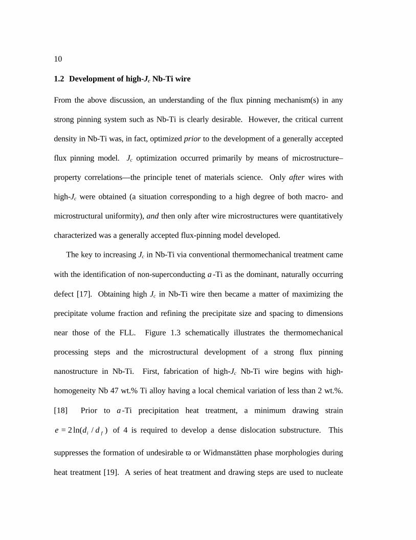
near those of the FLL. Figure 1.3 schematically illustrates the thermomechanical
processing steps and the microstructural development of a strong flux pinning
nanostructure in Nb-Ti. First, fabrication of high-Jc Nb-Ti wire begins with high-
homogeneity Nb 47 wt.% Ti alloy having a local chemical variation of less than 2 wt.%.
[18] Prior to α-Ti precipitation heat treatment, a minimum drawing strain
ε = 2 ln( / )d di f of 4 is required to develop a dense dislocation substructure. This
suppresses the formation of undesirable ω or Widmanstätten phase morphologies during
heat treatment [19]. A series of heat treatment and drawing steps are used to nucleate
11
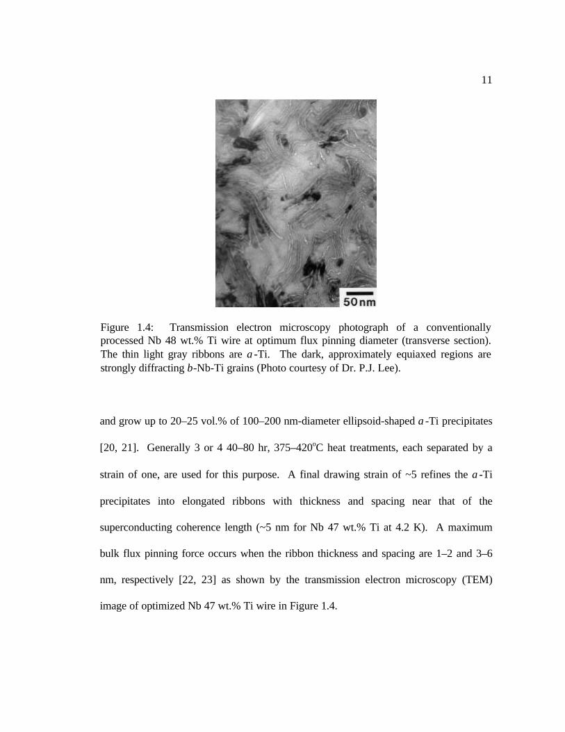
and grow up to 20–25 vol.% of 100–200 nm-diameter ellipsoid-shaped α-Ti precipitates
[20, 21]. Generally 3 or 4 40–80 hr, 375–420oC heat treatments, each separated by a
strain of one, are used for this purpose. A final drawing strain of ~5 refines the α-Ti
precipitates into elongated ribbons with thickness and spacing near that of the
superconducting coherence length (~5 nm for Nb 47 wt.% Ti at 4.2 K). A maximum
bulk flux pinning force occurs when the ribbon thickness and spacing are 1–2 and 3–6
nm, respectively [22, 23] as shown by the transmission electron microscopy (TEM)
image of optimized Nb 47 wt.% Ti wire in Figure 1.4.
Figure 1.4: Transmission electron microscopy photograph of a conventionallyprocessed Nb 48 wt.% Ti wire at optimum flux pinning diameter (transverse section).The thin light gray ribbons are α-Ti. The dark, approximately equiaxed regions arestrongly diffracting β-Nb-Ti grains (Photo courtesy of Dr. P.J. Lee).
12
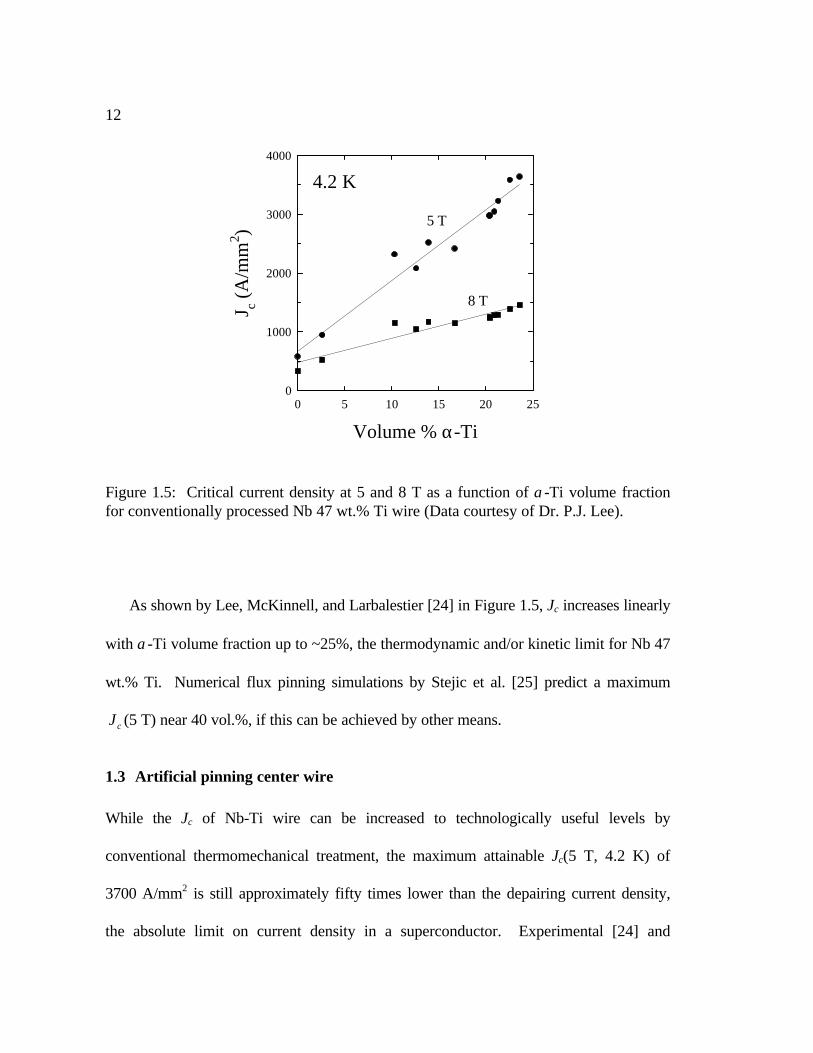
As shown by Lee, McKinnell, and Larbalestier [24] in Figure 1.5, Jc increases linearly
with α-Ti volume fraction up to ~25%, the thermodynamic and/or kinetic limit for Nb 47
wt.% Ti. Numerical flux pinning simulations by Stejic et al. [25] predict a maximum
Jc (5 T) near 40 vol.%, if this can be achieved by other means.
1.3 Artificial pinning center wire
While the Jc of Nb-Ti wire can be increased to technologically useful levels by
conventional thermomechanical treatment, the maximum attainable Jc(5 T, 4.2 K) of
3700 A/mm2 is still approximately fifty times lower than the depairing current density,
the absolute limit on current density in a superconductor. Experimental [24] and
Volume % α-Ti
0 5 10 15 20 25
J c (A
/mm
2 )
0
1000
2000
3000
4000
4.2 K
5 T
8 T
Figure 1.5: Critical current density at 5 and 8 T as a function of α-Ti volume fractionfor conventionally processed Nb 47 wt.% Ti wire (Data courtesy of Dr. P.J. Lee).

13
theoretical [25] predictions suggest that further increases in the volume fraction of α-Ti
should lead to further increases in Jc. In addition, alternative pin materials and pin
geometries may provide stronger elementary pinning interactions than the ribbon-shaped
α-Ti precipitates.
One route to higher performance is to replace the precipitates with better pins.
These so-called artificial pinning center (APC) superconductor designs do not suffer
from thermodynamic or kinetic restrictions and thus offer greater flexibility in the choice
of pinning center composition, volume fraction, and arrangement. Dorofejev et al. [26]
first incorporated artificial pinning centers into Nb-Ti wires using a mechanical assembly
technique, where the pinning centers were introduced as a starting component into the
interior of the superconductor. Although a thorough characterization of the
microstructure and superconducting properties was lacking, their pioneering study
proved the principle and quickly generated interest within the low temperature
superconductor community. Subsequent studies were initiated by Motowidlo et al. [27,
28], Cooley, Lee and Larbalestier [29, 30], Matsumoto et al. [31, 32, 33], and Wong et
al. [34, 35]. While the choice of pin geometry varied, as shown in Figure 1.6, the
fabrication methods used by each group are fundamentally the same. Each technique
requires a starting pin size large enough, generally 1–10 mm, for easy handling.
Consequently, very large strains of order 20–30 are required to reduce the artificial
pinning centers to the nanometer dimensions of the FLL, twice the strain needed for
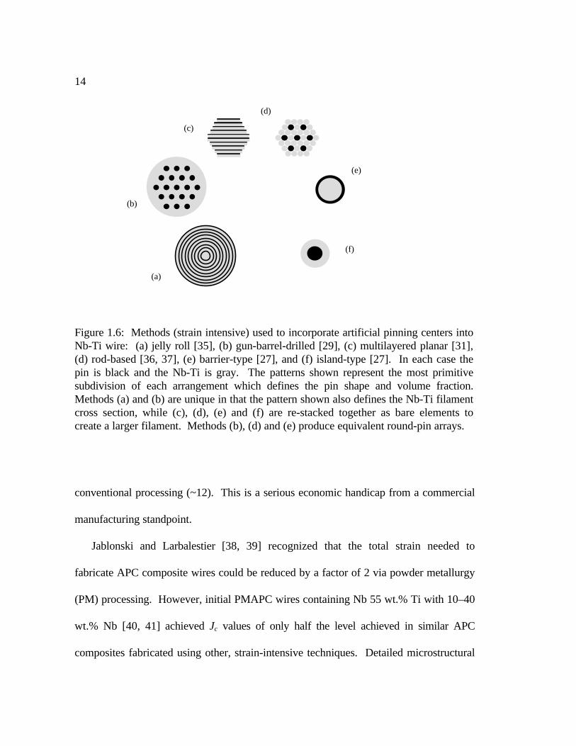
14
conventional processing (~12). This is a serious economic handicap from a commercial
manufacturing standpoint.
Jablonski and Larbalestier [38, 39] recognized that the total strain needed to
fabricate APC composite wires could be reduced by a factor of 2 via powder metallurgy
(PM) processing. However, initial PMAPC wires containing Nb 55 wt.% Ti with 10–40
wt.% Nb [40, 41] achieved Jc values of only half the level achieved in similar APC
composites fabricated using other, strain-intensive techniques. Detailed microstructural
(f)
(b)
(c)
(d)
(e)
(a)
Figure 1.6: Methods (strain intensive) used to incorporate artificial pinning centers intoNb-Ti wire: (a) jelly roll [35], (b) gun-barrel-drilled [29], (c) multilayered planar [31],(d) rod-based [36, 37], (e) barrier-type [27], and (f) island-type [27]. In each case thepin is black and the Nb-Ti is gray. The patterns shown represent the most primitivesubdivision of each arrangement which defines the pin shape and volume fraction.Methods (a) and (b) are unique in that the pattern shown also defines the Nb-Ti filamentcross section, while (c), (d), (e) and (f) are re-stacked together as bare elements tocreate a larger filament. Methods (b), (d) and (e) produce equivalent round-pin arrays.
15
analysis of PMAPC wires revealed that a broad distribution of pinning center thickness at
optimum size was likely responsible for the depressed Jc values. Presently, it is not
known whether a broad distribution in pin thickness is intrinsic to the powder metallurgy
process or is wholly due to characteristics of the starting powders.
A wide variety of APC compositions, fractions, and geometries have been used and
some considerable successes have been achieved. A multilayered APC structure [33]
consisting of Nb 50 wt.% Ti with 28 vol.% of Nb achieved 4250 A/mm2 (5 T, 4.2 K),
the highest value ever reported (prior to this thesis) for a round Nb-Ti wire. This high
value was achieved despite the fact that the composite Hc2 was ~1 T less than that of Nb
47 wt.% Ti. However, present APC designs have some drawbacks, not the least of
which results from the operation of the proximity effect [42, 43, 44, 45, 46].
1.3.1 Proximity-effect depression of Tc, Hc2
Most APC designs use Nb 47-50 wt.% Ti with 20-30 vol.% of Nb pins. At wire
diameters which give optimum Jc, the pin thickness is sufficiently small for proximity-
effect coupling to occur. Proximity-effect coupling of the pins to the matrix effectively
homogenizes the values of Hc2 and Tc, changing them from values of the matrix
composition to values representing a composite average [23]. In the case of Nb pins
coupled to Nb 47 wt.% Ti, a Nb-rich overall composition results. The homogenized
state should have a slightly higher Tc but a considerably reduced Hc2, as illustrated by the
plots of Tc and Hc2 versus composition in Figure 1.7 [23, 47]. Other pin materials, such
as Cu [48, 49], can reduce both Tc and Hc2 in even more marked fashion. Proximity-

16
effect coupling also occurs in conventional Nb-Ti where the α-Ti precipitates are
coupled to the matrix with composition ~Nb 39 wt.% Ti, but in this case the overall
composition is close to that which gives maximum Hc2. The proximity effect exerts a
beneficial effect in the conventional wire, serving to restore the high Hc2 that was lost
during the composition changes that accompany the precipitation heat treatments. So,
the key to optimizing Hc2 in APC wires thus appears to be in avoiding an overall
composition which departs significantly from Nb 44–48 wt.% Ti, where Hc2 reaches its
peak. One goal of this thesis is to explicitly test the proximity mixing hypothesis above
by fabricating Nb-pin APC composites designed for maximum Hc2 in the fully coupled
limit.
wt.% Ti
0 20 40 60 80 100
µ0
Hc2
(T)
Tc (
K)
4
5
6
7
8
9
10
11
12
Hc2 (4.2 K)
Tc
Figure 1.7: Critical temperature [23] and upper critical field at 4.2 K [47] as a functionof Nb-Ti composition.
17
1.3.2 The shape of Fp(H)
Another important difference between APC and conventional wires lies in the shape of
the bulk flux-pinning force curves. In particular, the value of field at which the
maximum pinning force (Fpmax) occurs is different. Conventional composites exhibit a
peak at ~0.5Hc2 while APC composites most often exhibit a peak at ~0.25Hc2. Flux
pinning in conventional Nb-Ti has long been explained with fluxon core pinning models
[10], for which Fpmax~0.5Hc2 appears naturally, as argued previously. This is seen
experimentally, as shown in Figure 1.8, and the presence of a h(1–h) shape of the bulk is
thought to validate the core pinning hypothesis. In addition, the α-Ti precipitate number
density far exceeds the number density of all other defects, and the functional
dependence of fp derived from Fp and the precipitate number density supports core
pinning. However, other data are not consistent with core pinning being the dominant
mechanism. For instance, the 1–4 nm thick α-Ti ribbons at optimum size, are too thin to
strongly interact with the 10 nm diameter fluxon cores at 4.2 K. In addition, Fp(H) data
near Tc yields F h hp ∝ −1 2 1/ ( ) rather than the h h( )1− functional dependence.
Since the nanostructure of APC composites is in fact very similar to that of
conventional composites, the different behavior of Fp(H) raised many questions. In
particular, the dominant pinning mechanism may be magnetic [50], rather than a core
mechanism. The importance of magnetic pinning interactions has recently been
completely reevaluated [51] and a new model has been introduced to describe the
behavior of both conventional and APC Nb-Ti. Cooley, Lee, and Larbalestier [52, 53]
18
explain the difference in bulk pinning force curves between conventional and APC Nb-Ti
as resulting from the different proximity lengths of pure Nb and α-Ti pins. This new
model makes testable predictions of the optimum pin design for any Nb-Ti composite,
and it proposes that APC Nb-Ti can be further advanced by reducing the electron mean
free path of the pin. Thus a second goal of this thesis is to test the predictions of the
magnetic pinning model.
1.4 Design of this thesis
This thesis follows two dissertations within our group on APC Nb-Ti wires. Cooley [29]
studied a gun-barrel-drilled composite with the most uniform nanometer scale pinning
µ0H (T)
0 2 4 6 8 10 12
Fp
(GN
/m3 )
0
5
10
15
20
4.2 K
3.4
εf = 1.1
2.5
4.4
5.1
Figure 1.8: Fp(H) as a function of final strain for conventionally processed Nb 48 wt.%Ti wire [10].

19
array to date, but for which the optimum Jc properties were achieved when the
superconducting filament diameter was of order λ (250 nm at 4.2 K). This sub-micron
filament size produced an undesirably large surface pinning contribution to the bulk
pinning force, thus complicating analysis of the pinning intrinsic to the pins. Jablonski
[39] developed a novel powder metallurgy approach which reduced the fabrication strain
needed to fabricate nanometer-scale pin arrays in wires by a factor of two. However the
broad pin thickness distributions produced by this process were detrimental to Jc. Many
of the lessons learned and techniques developed during the course of these two studies
were effectively utilized in the present study. To first order, we sought to make APC
composites with large (>>λ) filament diameters and uniform pin arrays in order to
circumvent the major obstacles encountered by Cooley and Jablonski. To this end, we
were successful—many thanks to Lance and Paul!
The remainder of this thesis is framed around the design, fabrication and
characterization of wires containing large (>>λ) Nb-Ti filaments with uniform pinning
centers arrays. The order follows a logical progression, beginning with a description of
APC wire design, fabrication and characterization techniques in chapter 2, followed by a
comprehensive study of the microstructure and properties of a preliminary composite
containing Nb 47 wt.% Ti with 24 vol.% Nb pins in chapter 3. This initial study
prompted three subsequent studies of more advanced composite designs described in
chapters 4–6. Detailed descriptions of the remaining chapters follow.
20
Chapter 2 describes the design and fabrication of Nb-Ti wires with round artificial
pinning centers and large (>>λ) filament diameters. Composite wire design and
fabrication issues related to monofilament and multifilament wire extrusion and drawing
are discussed. In addition, the techniques used to measure the transport critical current
density and magnetization are described.
Chapter 3 describes a comprehensive study of the microstructure and
superconducting properties evolution of a preliminary APC composite containing Nb 47
wt.% Ti with 24 volume percent of round Nb pins. Jc, Fp, and the irreversibility field
(H*) are analyzed as the nominal pin diameter is reduced from 165 to 15 nm. A large
discrepancy in Jc(dp, H) between composites which had received three or four warm
(650oC) in their fabrication was observed. The Jc depression was attributed to pin–
matrix interdiffusion caused by the fourth warm extrusion.
Chapter 4 discusses thermomechanical processing improvements designed to
minimize pin–matrix interdiffusion, and thereby strengthen fp. Accordingly, Jc increased
by 25–40% at all fields, rising from 3200 to 4600 A/mm2 at the benchmark field (5 T)
and temperature (4.2 K) and thus establishing a new high Jc for round-wire Nb-Ti.
However, just as in the earlier composite, the improved composite suffered from
depressed Jc at high-field for which two sources were identified: (1) Hc2 depression
caused by the matrix composition not being optimized for maximum Hc2 in the fully
coupled limit, and (2) a low-field maximum in Fp(H), as predicted by the magnetic
21
pinning model of Cooley, Lee and Larbalestier for short proximity length pins such as
Nb. Chapters 5 and 6 address each issue independently.
Chapter 5 addresses the proximity-effect depression of Hc2 and Tc observed in all
existing Nb-pin APC composites. In order to design for maximum Hc2 and Tc, the
starting Ti content of the matrix was increased from 47 wt.% to 62 wt.% Ti in order to
shift the composite composition closer to the optimum Hc2 composition of Nb 44 wt.%
Ti. A clear trend of increasing Hc2 with decreasing pin size was present in the Nb 62
wt.% Ti matrix APC composite, direct evidence of proximity-effect Hc2 enhancement.
However, the extent of enhancement was significantly less than predicted in the fully
coupled limit, even when the pin thickness was much smaller than ξ. The discrepancy
between predicted and observed behavior is evaluated within the context of proximity-
effect models for Nb/Ti thin film multilayers.
Chapter 6 then tests the magnetic pinning model proposed by Cooley, Lee, and
Larbalestier. The proximity length of pure Nb was decreased by 30% and 60% via
separate alloying additions of 7.5 wt.% Ta and 10 wt.% W, respectively. The functional
dependence of the bulk flux pinning force on field, dp and ξN agreed qualitatively with the
magnetic pinning model.
Chapter 7 summarizes the conclusions that can be drawn from this work.

22
23
2. APC wire design, fabrication, and
characterization
The basic premise governing APC wire fabrication is that a spatially uniform two-
dimensional array of Nb-Ti and a non-superconducting pin material can be assembled at
a macroscopic size, i.e. when the pins are 10–3–10–2 m in diameter, and then reduced
through a series of extrusion, drawing and re-stacking steps until the pin size and spacing
are comparable to the fluxon core diameter 2ξ and spacing a0 , i.e. 10–8 m at 4.2 K and
2 2 10 8. × − m at 5 T. No other metalworking process requires a comparably large
deformation strain of order 20–25 and only because of the extreme ductility of Nb-Ti
alloy can such a process be considered. The entire process is illustrated by the flow chart
shown in Figure 2.1.
24
Nb-
Ti
0
5
10
15
2
0
25
ε
106
1
05
104
103
102
1
0d p
(nm
) pin
or
Cu
Figu
re 2
.1:
Fab
rica
tion
flo
w c
hart
for
AP
C w
ires
. T
he b
ar s
how
n re
pres
ents
sta
ges
of th
e re
duct
ion
sequ
ence
; the
long
gra
yse
gmen
ts r
epre
sent
ext
rusi
on s
teps
, whi
le th
e sh
ort,
dark
er s
egm
ents
rep
rese
nt c
old
draw
ing
step
s. T
he h
oriz
onta
l arr
ows
indi
cate
whe
re th
e re
-sta
ckin
g st
eps
occu
rred
. T
he s
peci
fic
flow
cha
rt s
how
n co
rres
pond
s to
com
posi
tes
fabr
icat
ed in
Cha
pter
s 4–
6.

25
At the crux of the fabrication process are several sub-element re-stacking steps which
allow for simultaneous control over the pin, filament, and wire diameters. Each stage is
described below in general terms, with specific details provided in chapters 3–6 where
the specific composites are discussed.
2.1 Wire Design
The design of APC composite wires requires consideration on two size scales, the first
scale being the nanometer length scale of flux-pinning centers, as discussed above, and
the second being the micrometer subdivision of superconducting Nb-Ti filaments within
the Cu matrix. The following sub-sections detail the designs of the pin array and the
filament array.
2.1.1 Pinning array design
To first order, APC designs satisfy two basic criteria. Since vortices are uniformly
distributed in the flux line lattice, the pinning centers should also be uniformly distributed
in the superconducting matrix in order to maximize the number of vortex–pin
interactions. Second, most applications require isotropic flux pinning for any field
orientation perpendicular to the wire axis.
Despite the rather large number of APC designs shown in Figure 1.6, the effect of
starting pin arrangement has not been systematically studied. However, no design has
functioned particularly well or poorly, either. Complicating this issue is the fact that the
pinning center shape and arrangement at optimum size seldom resemble the shape

26
expected from the design, as shown in the few studies where optimized nanostructures
have been revealed by transmission electron microscopy [29, 39, 54]. Thus, it is still not
at all clear whether the starting pin geometry is important.
Our designs therefore emphasized uniform, isotropic pin arrangements. Round pins
are a good choice since their shape is well defined and the progressive degradation of
their shape with drawing strain can be routinely characterized with the image analysis
algorithms of Lee, Jablonski, and Larbalestier [55]. The island-type process [Figure
1.6(f)] is ideal since both the pin spacing and volume fraction are determined by the
diameters of the pin and the Nb-Ti tube. The rod-based process [Figure 1.6(d)] offers
less control over the pin spacing and volume fraction, but also offers the requirement of
using only rods for starting components; the difficulty associated with gun-drilling a Nb-
Ti tube is avoided. The composites in this thesis were assembled using both techniques.
In the early stages of fabrication process development, the rod-based technique was
used. Once the composite billet design and the thermomechanical parameters which
control deformation during extrusion and drawing were better understood, island-type
designs were chosen because of the more precise control over the pin diameter and
spacing they afforded.
2.1.2 Selection of pin material, pin fraction, and matrix composition
Since we had little previous experience with large-strain, multiple-extrusion APC
techniques, our first goal was to develop the fabrication process. To this end, Nb was
selected as the pinning center material due to its high ductility, and mechanical and

27
chemical compatibility with Nb 47 wt.% Ti. Since similar Nb-pin composites had been
fabricated previously by others using several different fabrication techniques, one goal of
our early work was to make a direct comparison of our composite to others. This
consideration also guided our initial selection of a 25% volume fraction and a Nb 47
wt.% Ti matrix composition. Once the processing parameters were well understood,
both the matrix and pin compositions were varied in subsequent composites with only
slight changes made to the processing parameters.
2.1.3 Process design
Since a typical single-stack reduction schedule used to make conventional Nb-Ti wires
allows for a total strain of 11–15 (e.g., reducing a 1.5–25 cm dia. billet to 0.1 mm dia.
wire), several re-stacking steps are necessary to accumulate the requisite strain of 20–30.
The number of stacking steps (n) required for this purpose partially depends on the
desired characteristics of the final wire, specifically the nominal pin diameter (dp), wire
diameter (dw), copper-to-superconductor ratio (R) and pin volume fraction (Vp). These
four parameters can be used to calculate the total number of pins (np):
( )n d d V Rp w p p= + −( )2 1
1 . (2.1)
np serves as a global design parameter and is used to quantify the relationship between n
and the number of elements per stack (ne) for each fabrication technique:
n n Ve p pn= −( ) rod-based (2.2a)
n ne pn= − island-type (2.2b)
28
Using typical final wire design parameters ( d p = 20 nm , dw = 80 µm , Vp = 0 25. , and
R = 1.5) the relationship between n and ne is shown graphically in Figure 2.2 for a rod-
based wire design. The choice of n was largely determined by cost. Figure 2.2 shows
the cost (in terms of total labor input to fabricate a given APC wire) as a function of n.
Cost is defined roughly by
cost (∝ + −n nen300 0 9) . . (2.3)
In practice, 3 or 4 stacking and extrusion steps were used, which corresponds to
minimum cost.
n
1 2 3 4 5 6 7
n e
101
102
103
104
105
cost
(ar
b. u
nits
)
0.00
0.25
0.50
0.75
1.00
1.25
1.50
1.75
2.00
cost
ne
Figure 2.2: Design considerations for APC wires. The number of stacked elements (ne)is plotted as a function of the number of extrusions (n) needed to manufacture an APCwire, using typical input parameters of dp=20 nm, dw=80 µm, Vp=0.25 and R=1.5. Alsoshown is the cost as a function of n, where cost (∝ + −n ne
n300 0 9) . . Note that the ne
scale is logarithmic while the cost scale is linear. In practice, 3 or 4 stacking andextrusion steps were used, corresponding to minimum cost.

29
It should be noted that the curves in Figure 2.2 correspond to absolute minimum
values. In practice, elements were stacked into hexagonal-shaped arrays to facilitate
subsequent stacking operations, thus imposing a geometrical constraint on ne. The
number of elements in a hexagonal array of radius r elements from center to corner is
given by:
n r rehex = − +3 3 12 (2.4)
which yields allowable ne values of 7, 19, 37, 61, 91, 127,…etc.
Thus far, this analysis has neglected consideration of the Nb-Ti filament diameter. As
discussed in chapter 1, in order to avoid surface pinning contributions to the bulk pinning
force, the filament diameter must be significantly larger than λ. Conversely, large-
diameter filaments are more susceptible to flux jump instability [56] at currents below Ic.
Most commercial superconducting wires have filament diameters which range from 5–
100 µm, providing a good guide for APC wire design. Here, the final filament diameter
range was determined by the extrusion stage at which the copper cladding was removed
prior to re-stacking. Prior to that step, a 55-filament stack was made to better
approximate a round filament, as shown in Figure 4.1(a).
2.2 Wire fabrication
2.2.1 Composite billet design
A hexagonal-shaped bundle of Nb-Ti and pin material rods [Figure 1.6(d)] was used to
assemble rod-based APC wires, while a rod of the pin material and a Nb-Ti tube [Figure
30
1.6(f)] were used to assemble island-type APC wires. In both cases the outer dimension
of the stack was designed to fit within a 15.6 mm O.D. copper can, this dimension fixed
by the 15.9 mm inner diameter of the extrusion chamber bore, the ~0.3 mm difference
used to accommodate thermal expansion of the billet during pre-heating, and the space
for the hydrostatic fluid. The inner diameter of the Cu can determined the composite
copper-to-superconductor ratio. Since Cu is significantly softer than Nb-Ti and the ratio
of their flow stresses depends on temperature, the volume ratio of the two metals and the
extrusion temperature control the uniformity of deformation during extrusion and
drawing. Choice of extrusion temperature is discussed in more detail in section 2.6.
2.2.2 Composite billet assembly
Figure 2.3 schematically illustrates the components of a typical extrusion billet. The
process and apparatus for billet fabrication by extrusion were based on methods
developed previously by Jablonski [39]. Extrusion cans were made by welding an end
cap onto one end of a Cu tube. The cans were welded in an argon-filled glove box using
a motor-driven fixturing assembly which rotated the can circumferentially at 6 RPM
beneath a stationary tungsten inert gas (TIG) welder. After end cap welding, the
extrusion can was removed from the glove box. Prior to billet assembly, all Cu
components were etched in a solution of 50% HNO3 and 50% H2O to remove surface
contamination and then ultrasonically cleaned in methanol. Nb-Ti and pin components
were not etched to avoid altering their dimensions, but were instead twice cleaned in
methanol.

31
Following rinsing and drying, billet components were transferred into the glove box
for composite assembly and nose cone welding. A nose cone was welded onto the can
using the same procedure as described previously for end-caps. After welding, fully
assembled extrusion billets were evacuated to ~10–2 Pa for ~5–10 hr with a diffusion
pump and temporarily sealed by cold forging a ~50 mm length of the evacuation tube,
the final seal being made by TIG welding over the seam. Finally, the evacuation tube
was swaged to ~2.5 mm diameter to allow for clearance through the extrusion die.
In order to remove much of the void space prior to extrusion, billets were compacted
to 240 MPa by cold isostatic pressing (CIP). In preparation for isostatic pressing, a billet
was inserted within a 20 mm diameter, 1 mm thick rubber CIP bag, then the bag was
evacuated and sealed with rubber bands. After isostatic pressing, the outer diameter of
the billet was machined to a final tolerance in preparation for extrusion. Whenever
Cu can Cu 30 wt.% Ni washer
hexagonal filamentary stacksupported by Cu shims
Cu nose cone withevacuation tube
Cu spacer 2-3 thin discs of Cu and Nb-Ti(not shown)
1 cm
Figure 2.3: Extrusion billet components prior to assembly.
32
possible, extrusion billets were machined to a uniform outer diameter of 15.6 ± 0.03 mm.
However, sometimes sections of the pressed billet compacted to less than 15.6 mm
diameter in juxtaposition to the hexagonal-shaped filament bundle contained within. In
that case, the length of the billet adjacent to the filaments was machined to a slightly
smaller diameter, typically 14.5–15.0 mm, while each end was machined to 15.6 mm to
allow for concentric alignment of the billet within the extrusion chamber. A compound
angle (35o / 40o half angle) was machined into the nose cone to provide a good seal with
the extrusion die (37.5o half angle).
2.2.3 Extrusion
As discussed earlier, the large reduction strains required for APC wire fabrication
generally require 2–4 element re-stacking steps. In order to facilitate strong bonding
amongst the elements and minimize end losses, each re-stack is usually extruded warm
(<0.5Tm, where Tm≡melting temperature). Moreover, the bonding of bare Nb-Ti
elements, a key requirement for maintaining a large (>>λ) Nb-Ti filament size, is
extremely difficult, if not impossible [57], without warm extrusion or elevated
temperature sintering.
Uniform extrusion of bimetallic composites becomes increasingly difficult as the ratio
of flow stresses becomes large, even for simple axisymmetric deformation processes such
as extrusion and drawing. Analytical solutions for bimetallic composite extrusion and
drawing, and analysis of common composite failure mechanisms are covered extensively
by Avitzur [58, 59, 60, 61, 62]. However, many variables enter the deformation

33
equations, several of which are difficult to quantify. In the present work, several
variables such as die angle and reduction ratio were selected according to previous
guidelines provided by Jablonski [39], who utilized a compendium of data provided by
Collings [63].
Homogeneous or sound composite flow is the principal objective of any extrusion,
thus, to first order the extrusion parameters were chosen to satisfy this condition. The
yield strength of face-centered cubic (fcc) metals such as Cu is rather temperature-
independent to high homologous temperatures while that of body-centered (bcc) cubic
metals such as Nb and Nb-Ti decreases as a result of thermally activated slip [64].
Therefore, increasing the extrusion temperature decreases both the overall flow stress
and the flow stress differential between Nb-Ti and Cu and expands the processing
parameter space for homogenous composite deformation. In practice, conventional Nb-
Ti composites are usually extruded at 500–650 oC [63].
However, elevated temperatures can adversely affect the APC structure. Secondary
phase (e.g. α-Ti) precipitation, interdiffusion or reaction between the Nb-Ti and the
pinning centers, and recrystallization of the Nb-Ti are all possible consequences of
elevated temperature processing. Each serves to degrade the APC structure. In addition
to these intrinsic effects, the formation of brittle Cu-Nb-Ti intermetallic compounds [65,
66] at the Cu–superconductor interface can lead to filament sausaging [67, 68, 69],
which places an extrinsic limit on Jc. Thus, to second order, the extrusion parameters
were selected to avoid or at least minimize all of these deleterious side effects.
34
10-24
10-22
10-20
10-18
10-16
Atomic Percent Niobium
0 10 20 30 40 50 60 70 80 90 100
Tem
pera
ture
(o C
)
400
600
800
1600
1800
2000
2200
2400
2600
10- 14
10-12
cm2 /s
α+β
β
L
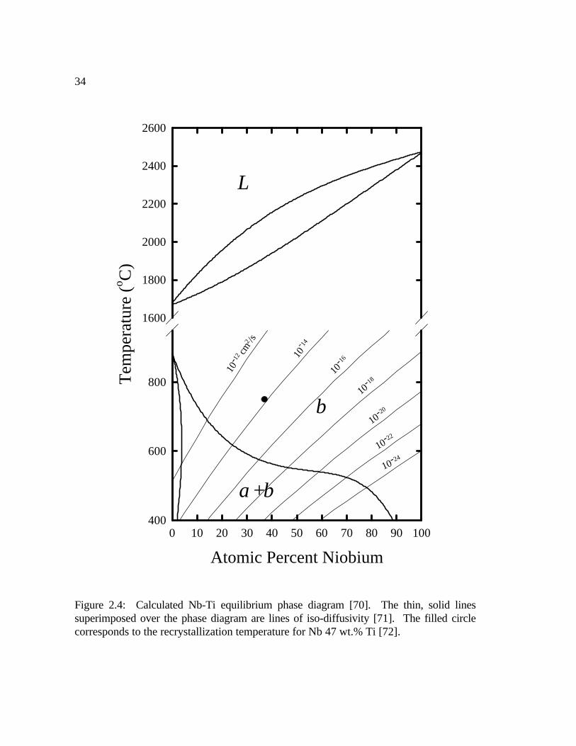
Figure 2.4: Calculated Nb-Ti equilibrium phase diagram [70]. The thin, solid linessuperimposed over the phase diagram are lines of iso-diffusivity [71]. The filled circlecorresponds to the recrystallization temperature for Nb 47 wt.% Ti [72].

35
As the above discussion shows, the selection of an appropriate extrusion temperature
requires consideration of the thermodynamics and recrystallization kinetics of the Nb-Ti
system. As shown by the Nb-Ti equilibrium phase diagram [70] in Figure 2.5, the α–β
transus temperature decreases with increasing Nb content. α-Ti can also be avoided at
lower temperatures because the precipitation is kinetically limited. Both temperature
boundaries depend on the Nb-Ti alloy composition and are approximately 550 and 350
oC, respectively, for Nb 47 wt.% Ti. Nb-Ti interdiffusion [71] and Nb-Ti-Cu
intermetallic formation [66] have a typical Arrhenius dependence on temperature, thus
lower temperatures are preferred. A maximum upper limit is the Nb-Ti recrystallization
temperature of 750 oC for Nb 47 wt.% Ti [72]. These considerations effectively set the
desirable extrusion temperature range at either below 300 oC or between 550–700 oC,
the former interval being preferred in order to minimize interdiffusion and/or reaction. A
series of initial scoping composites extruded at 250 oC (corresponding to the maximum
rated temperature of our extrusion chamber) broke up after 2 or 3 extrusions.
Subsequently, the extrusion temperature was raised to 650 oC by externally preheating
the billets. This step led to the successful fabrication of our preliminary composite
discussed in chapter 3.
Composite billets were extruded using a reverse hydrostatic extrusion press [73]
featuring a temperature-compensated extrusion chamber [74] and a rated maximum
extrusion pressure of 2 GPa. Billets were preheated for 15–20 minutes at the desired
extrusion temperature. Billets extruded at 250 oC were preheated in the extrusion
36
chamber, which was in every case preheated to 250 oC. Billets extruded at higher
temperatures were preheated in an external furnace with flowing argon and then
transported quickly (10–20 s) to the chamber with a stainless steel loading tool. Billets
were extruded at ~1 cm/s (billet velocity) using an area reduction ratio of 10 or 15 and a
die half angle of 37.5o. Extruded wires were immediately water quenched to avoid the
precipitation of second phases.
2.2.4 Wire drawing and re-stacking
Prior to wire drawing, 3–6 cm was cropped from the front and back of the extruded
wire. These regions comprised zones of non-uniform deformation, or “end effects”.
Wires were then scoured with an abrasive pad and wiped clean in order to remove the
surface layer of copper oxide that was usually present following. Wires were drawn at
~5 cm/s using a 20% area reduction ratio per die pass and 11.5o die half angle.
Wire was drawn to the appropriate diameter for re-stacking, usually 1–1.5 mm
diameter. The resulting length of wire was then divided by the number of filaments
required for the next stack, plus a few extra. Seven filaments, corresponding to the
center-most filaments in the stack, were cut 6.4 mm longer than the rest. These
filaments protruded through a Cu 30 wt.% Ni washer (shown in Figure 2.3) at the front
of the billet and served to reduce the breakthrough extrusion pressure at the front of the
filamentary stack, a technique commonly used in industry for large scale billets. The Cu
was then completely etched off using a mixture of 50% HNO3 and 50% H2O depending

37
on whether the wire was to be subsequently incorporated into a monofilament or a
multifilament composite. One exception to this procedure is outlined in the next section.
2.2.5 Reduction of copper-to-superconductor ratio
As a general rule, the R values of 1–1.5 used for homogenous deformation of extruded
monofilamentary APC composites were also appropriate for homogenous deformation
during drawing. However, the same was not true for multifilamentary composites,
where excessive interfilamentary copper can produce uneven stress distributions in the
plane transverse to the drawing direction, and ultimately lead to filament sausaging.
Gregory et al. [75] associated a filament spacing-to-diameter ratio (s/d) of 0.12,
corresponding to a local R value of ~0.5, with high-Jc fine filamentary Nb-Ti wire. In
addition, mechanical modeling of Nb-Ti composites by Guo and Warnes [76] showed
that a decreasing s/d reduces the macroscopic stresses in the plane normal to the wire
axis, thus promoting more uniform composite deformation.
In order to prevent filament sausaging in multifilamentary APC wire, we reduced the
local copper-to-superconductor ratio to ~0.5 following extrusion through partial removal
of the copper cladding. To remove copper in a controlled fashion, the extruded wire was
immersed in a nitric acid/distilled water solution and rotated circumferentially via a
motorized belt drive. This method produced excellent longitudinal and diametric
variations of less than 5% and 2%, respectively, once the optimum etch concentration
(30% HNO3 and 70% H2O) and rotation speed (10–20 RPM) were experimentally

38
determined. For example, the diameter of as-extruded 70 cm long wire was typically
reduced from 5.1 to 3.75 mm in approximately 2 hr.
2.2.6 Multifilament wires
In several circumstances, 7 or 19-filament multifilament wires were fabricated by cold
drawing. In preparation for stacking, the copper-to-superconductor ratio of the
extruded monofilamentary wire was reduced to an appropriate value as discussed in the
previous section. After etching, the wire was drawn down to 1.63 mm diameter and then
drawn through a hexagonal-shaped die (1.4 mm flat-to-flat dimension) The wire was cut
into 18 to 30 cm lengths for stacking inside a Cu tube (5.8 mm O.D. × 4.3 mm I.D. for a
7 filament stack and 8.2 mm O.D. × 7.1 mm I.D. for a 19 filament stack). In order to
circumvent the contact of drawing lubricant with the back end of the composite, the tube
was cut ~15 cm longer than the filaments and the back end was plugged with piece of
modeling clay. Prior to assembly, the copper-clad filaments and tube were etched lightly
in 50% HNO3 and 50% H2O, rinsed in methanol, and dried. Immediately afterward, the
filaments were stacked, clad in Cu, and drawn through at least ten die passes; it was
critical to perform these final steps quickly to obtain strong mechanical bonds between
filaments, particularly when the ambient humidity was high. Wire breaks occurred
infrequently during multifilament drawing, and when they did occur it was almost always
a result of weak interfilamentary bonding as inferred from observing the distributed,
intrafilamentary fractures.
39
2.3 Characterization techniques
2.3.1 Transport Jc measurements
Transport critical current measurements followed standard methods established in our
lab over the past decade. Sixty cm long wire samples were wound around and soldered
to a sample holder. The sample holder consisted of a 34.9 mm diameter, 0.8 mm wall
thickness stainless steel tube with thick copper rings soldered to each end. This design
provided secure sample mounting, good current transfer from the leads to the sample,
and a low resistance parallel shunt for the transport current in order to prevent sample
burnout above Ic. A helical groove with a twist pitch of 3.15 turns per centimeter
positioned the samples on the stainless steel tube.
The applied field for transport Jc measurements was supplied by either a 12 or a 14 T
(4.2 K) superconducting solenoid manufactured by Oxford Instruments. Four voltage
taps were soldered to the sample at 11 cm intervals that corresponded to successive
turns around the helical sample. The maximum tap spacing of 33 cm was used for most
measurements of the voltage (V). The transport current (I) was determined by
measuring the voltage across a calibrated shunt resistor connected in series to the power
supply. A computer-controlled interface was used to ramp the transport current and
acquire the V(I) data from two digital voltmeters connected to computer via a GPIB
interface. V(I) curves were fitted with the power law expression, V I n∝ , in the
superconducting-to-normal transition region. Jct was determined by the intersection of
the fitted data with a 10–14 Ω-m resistivity criterion, using the superconductor cross-
40
sectional area as the characteristic cross-section for determining the resistivity criterion.
Wire diameters were measured to a precision of 0.0005 mm using a calibrated
micrometer.
Copper-to-superconductor area ratios were determined by weighing a length of wire,
etching the Cu off using a mixture of 50% HNO3 and 50% H2O, and weighing the
superconductor. R was calculated by:
R m m D DCu c c Cu= ( )( ) (2.5)
where mCu, mc and DCu, Dc are the masses and densities of copper and the
superconductor (Nb-Ti matrix plus pin), respectively. Mass measurements were made
using an electronic balance with an sensitivity of 0.1 mg. Samples typically weighed 0.5
g. A density of 8.95 g/cm3 was used for copper, while the superconductor density was
calculated using the composite volume-fraction rule [64]:
D D V D Vc p p m p= + −( )1 , (2.6)
where Dp and Dm are the densities of the pin and the Nb-Ti alloy matrix, respectively.
2.3.2 Magnetization measurements
Magnetization measurements were used to determine Hc2 and the irreversibility field
(H*). In addition, Jc can be determined indirectly through application of an appropriate
critical state model to the irreversible magnetization hysteresis (∆M). This method for
determining the magnetization critical current density (Jcm) is particularly attractive since,
unlike Jct, it can be measured continuously with field. For the present work, a vibrating
sample magnetometer (VSM) was used to measure M(H) loops at temperatures from
41
2.2–10 K and fields from 0 to Hc2(T). The reversible magnetization data at fields near
and above the field of loop closure (i.e. ∆M=0) were used to determine H* and Hc2,
while the irreversible magnetization was used to extract Jcm at 4.2 K and at reduced
temperature. The VSM system in our laboratory was designed and constructed by
McKinnell [77] and consists of a Princeton Applied Research Model 155 VSM vibrator
head assembly and supporting electronics custom fit to an Oxford 14 T superconducting
magnet and variable temperature insert. A detailed description of this system is given in
reference [77].
Magnetization critical current density was derived from the irreversible
magnetization hysteresis ∆M(H) using the Bean critical state model for a
superconducting cylinder in perpendicular field [78]:
J H T M H T dcm f( , ) ( , )= 3 4π∆ (2.7)
Jcm measurements made on conventionally processed Nb 44-58 wt.% Ti wires [77] and
sub-micron filament diameter APC wires with Nb pinning centers [29] have shown good
agreement with Jct measurements made on the same samples. However, in this study, we
found that some wires exhibited a large discrepancy between the shape of Jct(H) and
Jcm(H). A study of PMAPC wires [79] showed a similar discrepancy. For the present
wires, analysis of the dependence of M(H) on sample length showed this difference could
be attributed to the highly anisotropic critical current densities that flow parallel and
perpendicular to the pinning centers. An experimental and theoretical analysis of this
effect, showing the role that the anisotropic pinning nanostructure plays in determining

42
the longitudinal and transverse critical current densities of optimized Nb-Ti wire, is
presented in Refs. [80, 81].
43
3. Properties of Nb-Ti wires with Nb artificial
pinning centers
This chapter describes the development of the microstructure and superconducting
properties of our preliminary Nb 47 wt % Ti composite wire containing 24 vol. % of Nb
pinning centers. This combination was chosen because of its similarity to composites
fabricated in other studies using different methods, thus allowing for more direct
comparisons of properties. One goal has been to make a thorough nanostructural
characterization so that the pinning center size and shape at optimum wire sizes are
known and not just assumed. Such characterizations are seldom performed at optimum
size. A second goal of this study was to measure the Jc, Fp and Hc2 at reduced
temperatures, not just at 4.2 K, so that the properties of conventional and APC wires
could be compared at constant Hc2. To perform the reduced temperature study we relied
primarily on magnetization measurements. During the course of taking data, the
44
hysteretic magnetization was found to be strongly dependent on the sample length. An
experimental and theoretical analysis of this effect, showing the role that the anisotropic
pinning nanostructure has on the longitudinal and transverse critical current densities of
optimized Nb-Ti wires, is presented in Refs. [80, 81]. This effect is taken into account
here.
3.1 Experimental Design
An APC composite containing a matrix of Nb 47 wt % Ti and 24 vol % of round Nb
pins was fabricated using the rod bundling process discussed in chapter 2. Thirty-one 1-
mm diameter Nb rods were arranged in a hexagonal array within a bundle of 96 Nb 47
wt. % Ti rods such that the center-to-center pin spacing was 1.53dp. This 127-rod stack
was canned in Cu, and extruded at 650 oC using an area reduction ratio of 15. The
extruded wire was drawn to 1 mm diameter, cut lengthwise into 127 pieces and the Cu
was dissolved away in a 1:1 mixture of HNO3 and H2O. The hexagonal-shaped Nb-
Ti/Nb filaments were re-stacked, canned in Cu and a second extrusion was made under
the same conditions. After a third draw, re-stack, and extrusion sequence the
monofilament wire contained ~5×10⁵ Nb pinning centers. A part of this wire was drawn
to 0.08 mm diameter, while the rest was cut into seven pieces and extruded for a fourth
time. The fourth extrusion wire was then drawn to 0.08 mm diameter. Table 3.1 gives
fabrication details for each composite.
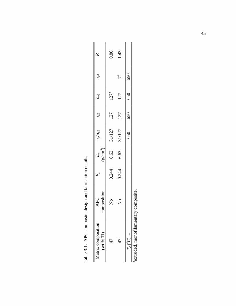
45
Tabl
e 3.
1: A
PC
com
posi
te d
esig
n an
d fa
bric
atio
n de
tail
s.
Mat
rix
com
posi
tion
(wt.%
Ti)
AP
Cco
mpo
siti
onV
pD
c
(g/c
m3 )
n p/n
e1n e
2n e
3n e
4R
47N
b0.
244
6.63
31/1
2712
712
7a0.
86
47N
b0.
244
6.63
31/1
2712
712
77a
1.43
Te (
o C)
→65
065
065
065
0a ex
trud
ed, m
onof
ilam
enta
ry c
ompo
site
.
46
Magnetic moments were measured on wire samples using the vibrating sample
magnetometer. Long wire samples, ranging from 56 mm in length for the 0.360 mm
diameter wire to 300 mm for the 0.080 mm diameter wire, were wound into 3 mm
diameter, 1 mm long open-circuit coils. Long wire samples were used for two reasons:
Longer samples provide a larger sample moment, giving higher signal resolution. More
importantly, it has been demonstrated for this same set of samples, that the
magnetization of APC wires can be a very strong function of the wire length-to-diameter
ratio [80]. Long lengths give better agreement between the Jct and the magnetization
critical current density Jcm. The sample-length dependence comes from the fact that the
magnetization-induced current must cross the filament in a direction perpendicular to the
wire axis towards the ends of each filament and because the anisotropic pinning
nanostructure of the wires produces a Jc perpendicular to the axis of the pinning centers
which is up to ~100 times less than that flowing parallel to the pinning centers along the
wire axis. To obviate these concerns, moment measurements were made with the
applied field parallel to the coil axis on long samples, so that the field was perpendicular
to the long wire axis and currents were induced to flow along the whole wire length. A
field sweep rate of 0.05 T/s was used, except near Hc2, where it was reduced to 0.02 T/s
to increase the field resolution in the region of magnetization loop closure. The
magnitude of the hysteretic moment depended only weakly on the field sweep rate for
these APC monofilament samples. Magnetization critical current densities were derived
from the hysteretic magnetization of the long samples using the Bean model for a
47
cylindrical superconductor in perpendicular field (Equation 2.7). Magnetization runs
were made at temperatures from 3–10 K in fields up to 12 T. Transverse wire cross-
sections were analyzed by Scanning (SEM), Field Emission Scanning (FESEM) and
Transmission Electron Microscopy (TEM).
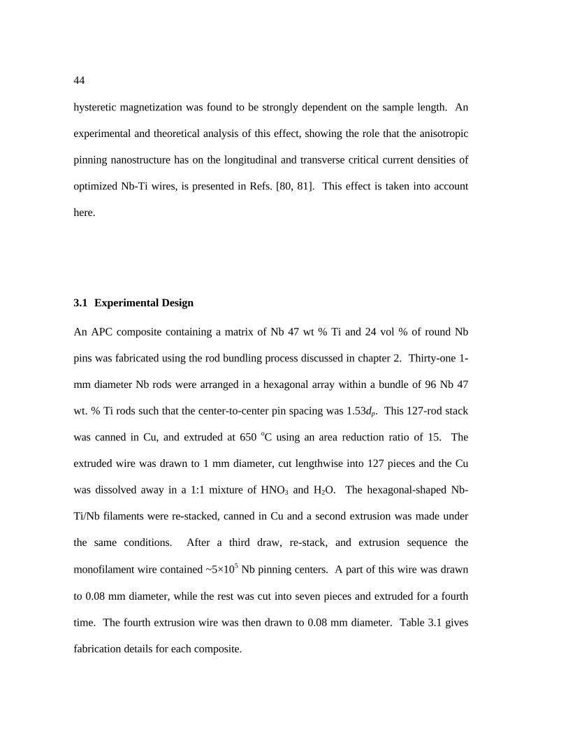
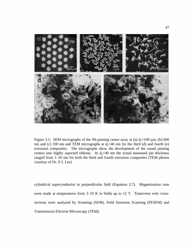
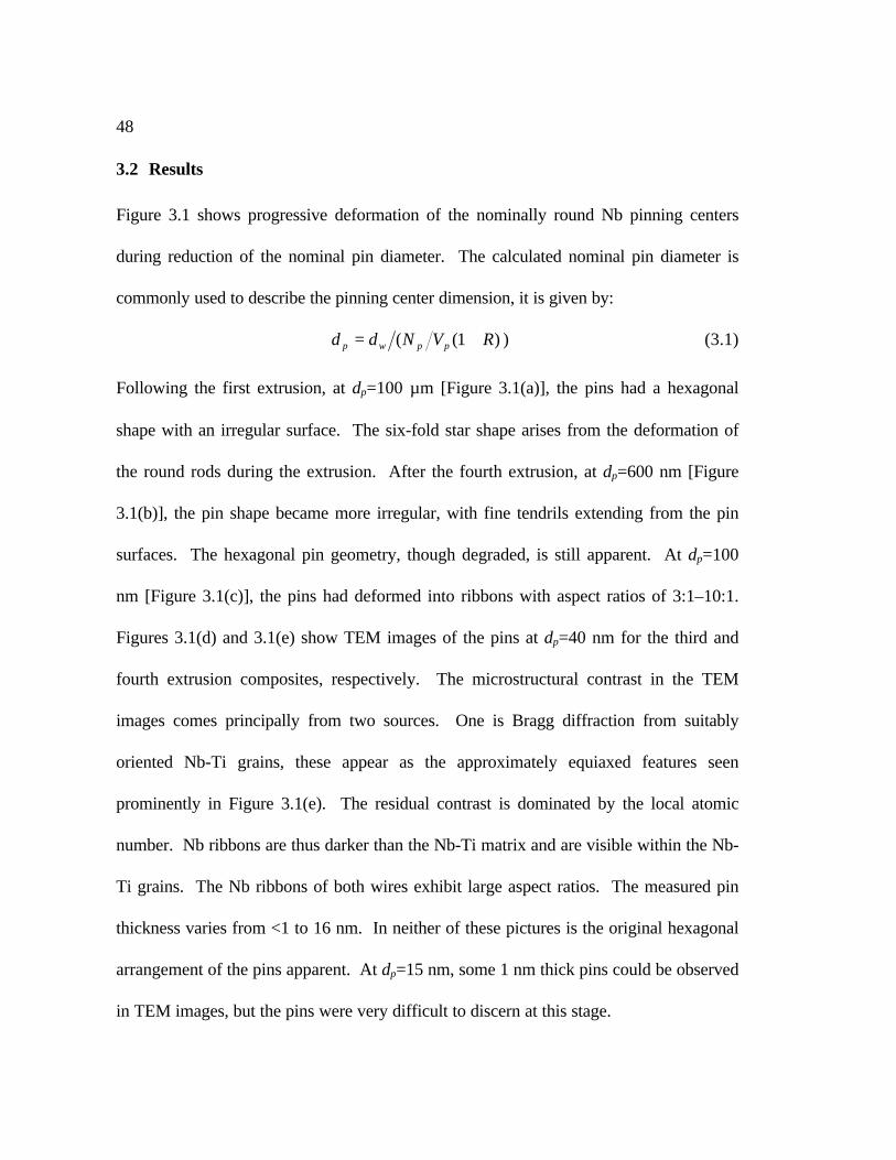
Figure 3.1: SEM micrographs of the Nb pinning center array at (a) dp=100 µm, (b) 600nm and (c) 100 nm and TEM micrographs at dp=40 nm for the third (d) and fourth (e)extrusion composites. The micrographs show the development of the round pinningcenters into highly aspected ribbons. At dp=40 nm the actual measured pin thicknessranged from 1–16 nm for both the third and fourth extrusion composites (TEM photoscourtesy of Dr. P.J. Lee).
48
3.2 Results
Figure 3.1 shows progressive deformation of the nominally round Nb pinning centers
during reduction of the nominal pin diameter. The calculated nominal pin diameter is
commonly used to describe the pinning center dimension, it is given by:
d d N V Rp w p p= +( ( )1 ) (3.1)
Following the first extrusion, at dp=100 µm [Figure 3.1(a)], the pins had a hexagonal
shape with an irregular surface. The six-fold star shape arises from the deformation of
the round rods during the extrusion. After the fourth extrusion, at dp=600 nm [Figure
3.1(b)], the pin shape became more irregular, with fine tendrils extending from the pin
surfaces. The hexagonal pin geometry, though degraded, is still apparent. At dp=100
nm [Figure 3.1(c)], the pins had deformed into ribbons with aspect ratios of 3:1–10:1.
Figures 3.1(d) and 3.1(e) show TEM images of the pins at dp=40 nm for the third and
fourth extrusion composites, respectively. The microstructural contrast in the TEM
images comes principally from two sources. One is Bragg diffraction from suitably
oriented Nb-Ti grains, these appear as the approximately equiaxed features seen
prominently in Figure 3.1(e). The residual contrast is dominated by the local atomic
number. Nb ribbons are thus darker than the Nb-Ti matrix and are visible within the Nb-
Ti grains. The Nb ribbons of both wires exhibit large aspect ratios. The measured pin
thickness varies from <1 to 16 nm. In neither of these pictures is the original hexagonal
arrangement of the pins apparent. At dp=15 nm, some 1 nm thick pins could be observed
in TEM images, but the pins were very difficult to discern at this stage.
49
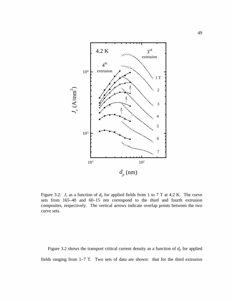
Figure 3.2 shows the transport critical current density as a function of dp for applied
fields ranging from 1–7 T. Two sets of data are shown: that for the third extrusion
dp (nm)
101 102
J c (A
/mm
2 )
103
104
3rd
extrusion
4th
extrusion
1 T
4.2 K
7
6
5
4
3
2
Figure 3.2: Jc as a function of dp for applied fields from 1 to 7 T at 4.2 K. The curvesets from 165–40 and 60–15 nm correspond to the third and fourth extrusioncomposites, respectively. The vertical arrows indicate overlap points between the twocurve sets.
50
covers the range of dp from 165 to 40 nm and that for the fourth ranges from 60 to 15
nm. Jc increases at all fields except 1 T with decreasing dp for the third extrusion
composite. At 1 T, the peak Jc was 20 kA/mm2 for dp=50 nm, while at 5 T, it was 3.2
kA/mm2 for dp=35 nm. In the pin diameter interval where the third and fourth extrusion
dp values overlap, dp=40–60 nm, there is poor agreement between the data. There is also
a crossover in Jc(dp) as the field is increased. From 1–3 T the third extrusion composite
Jc values exceed those of the fourth. From 3–5 T, crossover points are indicated by the
vertical arrows in Figure 3.2 and from 5–7 T, the fourth extrusion Jc values exceed those
of the third. The fourth extrusion composite exhibits Jc peaks at progressively smaller dp
values as the field is increased, where peaks of 40, 35, 25 and 17 nm occur for fields of
4, 5, 6, and 7 T, respectively. As is clear from Figure 3.1, the actual pin thickness is, in
all cases, much smaller than dp.
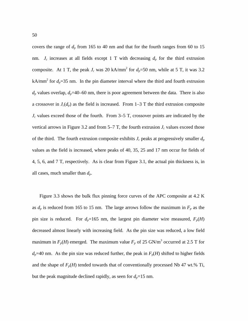
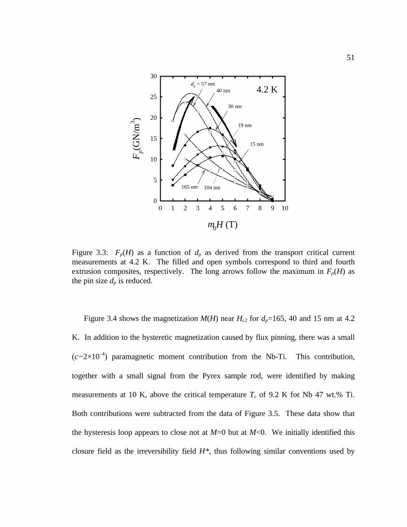
Figure 3.3 shows the bulk flux pinning force curves of the APC composite at 4.2 K
as dp is reduced from 165 to 15 nm. The large arrows follow the maximum in Fp as the
pin size is reduced. For dp=165 nm, the largest pin diameter wire measured, Fp(H)
decreased almost linearly with increasing field. As the pin size was reduced, a low field
maximum in Fp(H) emerged. The maximum value Fp of 25 GN/m3 occurred at 2.5 T for
dp=40 nm. As the pin size was reduced further, the peak in Fp(H) shifted to higher fields
and the shape of Fp(H) tended towards that of conventionally processed Nb 47 wt.% Ti,
but the peak magnitude declined rapidly, as seen for dp=15 nm.
51
Figure 3.4 shows the magnetization M(H) near Hc2 for dp=165, 40 and 15 nm at 4.2
K. In addition to the hysteretic magnetization caused by flux pinning, there was a small
(χ~2×10⁻⁴) paramagnetic moment contribution from the Nb-Ti. This contribution,
together with a small signal from the Pyrex sample rod, were identified by making
measurements at 10 K, above the critical temperature Tc of 9.2 K for Nb 47 wt.% Ti.
Both contributions were subtracted from the data of Figure 3.5. These data show that
the hysteresis loop appears to close not at M=0 but at M<0. We initially identified this
closure field as the irreversibility field H*, thus following similar conventions used by
4.2 K
µ0H (T)
0 1 2 3 4 5 6 7 8 9 10
Fp(
GN
/m3 )
0
5
10
15
20
25
30dp = 57 nm
40 nm
104 nm
19 nm
30 nm
165 nm
15 nm
Figure 3.3: Fp(H) as a function of dp as derived from the transport critical currentmeasurements at 4.2 K. The filled and open symbols correspond to third and fourthextrusion composites, respectively. The long arrows follow the maximum in Fp(H) asthe pin size dp is reduced.
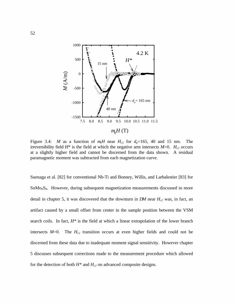
52
Suenaga et al. [82] for conventional Nb-Ti and Bonney, Willis, and Larbalestier [83] for
SnMo6S8. However, during subsequent magnetization measurements discussed in more
detail in chapter 5, it was discovered that the downturn in ∆M near Hc2 was, in fact, an
artifact caused by a small offset from center in the sample position between the VSM
search coils. In fact, H* is the field at which a linear extrapolation of the lower branch
intersects M=0. The Hc2 transition occurs at even higher fields and could not be
discerned from these data due to inadequate moment signal sensitivity. However chapter
5 discusses subsequent corrections made to the measurement procedure which allowed
for the detection of both H* and Hc2 on advanced composite designs.
µ0H (T)
7.5 8.0 8.5 9.0 9.5 10.0 10.5 11.0 11.5
M (
A/m
)
-1500
-1000
-500
0
500
1000
15 nm
dp= 165 nm
H*
40 nm
4.2 K
Figure 3.4: M as a function of µ0H near Hc2 for dp=165, 40 and 15 nm. Theirreversibility field H* is the field at which the negative arm intersects M=0. Hc2 occursat a slightly higher field and cannot be discerned from the data shown. A residualparamagnetic moment was subtracted from each magnetization curve.

53
Table 3.2 lists the measured H*(4.2 K) values as a function of nominal pin diameter
and temperature. µ0H* decreased from 10.3 to 9.5 to 9 T in going from dp=165 to 40 to
15 nm. For comparison, µ0H* for an optimized, conventionally processed wire at 4.2 K
is 10.7 T [84], a value of 1.2 T higher than the highest flux pinning (dp=40 nm) APC
sample. This strong suppression of H* in the APC composite complicates direct
comparison of APC and conventional wire properties.
3.3 Discussion
3.3.1 Microstructure
In this study, as in the few other studies which have explicitly observed the
microstructure at optimum wire size, it is abundantly clear that the real pin thickness is
considerably smaller than the round wire approximation, dp. The ribbon-like shape
developed by the Nb pinning centers is a general consequence of the <110> drawing
texture which develops in body centered cubic (bcc) metals subjected to the axially
Table 3.2: Irreversibility field as a function temperature for the APC wires at dp=165,40, and 15 nm and for an optimized, conventionally processed Nb 47 wt.% Ti wire at 4.2K.
dp (nm) µ0H* (T)
4.2 K 3.5 K 3 K165 10.3 L L40 9.5 10.7 L15 9.0 9.8 11.0
conventional Nb 47 wt.% Ti 10.7 L L

54
symmetric deformation of wire drawing [85, 86, 87]. In the early stages of drawing,
individual grains rotate, such that a <110> direction is aligned with the drawing axis.
Slip is then restricted to the two <111> directions which lie within the 110 plane
containing the <110> texture. The resultant plane strain deformation, combined with the
requirement of grain boundary continuity, forces the grains to intercurl, slowly
transforming into ribbons. In the case of the conventionally produced α+β two-phase
microstructure, the bcc β-Nb-Ti grain texture development causes the hexagonal close
packed α-Ti precipitates to transform into ribbons. In the APC composite, both Nb and
Nb-Ti are bcc, so it is likely that both pin and matrix contribute to the ribboning, as is the
case for Nb diffusion barriers in conventionally processed Nb-Ti wire [88, 89].
It is worth noting that the pin shape seen here, at least in the later stages of
development, parallels that seen in an earlier study by Cooley et al. of a somewhat similar
APC composite. In that case the pins of Nb 1 wt.% Ti were inserted into gun-barrel-
drilled holes and, aside from the initial warm extrusion of the original 150 mm diameter
Nb 47 wt.% Ti / Nb 1 wt.% Ti, all subsequent composite fabrication was done by cold
drawing. The shape of nominal 600 and 100 nm diameter pins of the present composite
are comparable to the shape of the 200 and 32 nm diameter pins of the earlier study.
The difference in the onset of pin shape degradation is likely due to differences in
processing methods, for in the present case, the pins were given an anneal at ~1 mm
diameter just prior to the stacking of the billet and three or four warm (650 oC) extrusion
steps were then used during wire reduction, thereby increasing the tendency for
55
polygonization or recovery of the Nb-Ti grains, either of which would increase the ratio
of the Nb-Ti grain size to Nb-pin diameter and cause more rapid pin shape degradation.
Thus the use of the nominal pin diameter as a quantitative tool can be somewhat
misleading, since two APC composites of not greatly dissimilar design can have
significantly different pinning microstructures for the same value of dp. However, the
use of dp is so widespread in the literature and there is so little quantitative microscopy
near optimum sizes that it is still useful to report properties as a function of dp.
Quantitative understanding of the dependence of properties on microstructure clearly
requires observation of the microstructure.
The maximum Fp for the APC composite occurs for dp=40 nm where the actual
measured pin thickness is quite variable, ranging from <1 to 16 nm as shown in Figures
3.1(d)–(e). This large pin thickness range contrasts strongly with the thinner, more
uniform pins observed in optimized, conventionally processed Nb 47 wt.% Ti, where the
α-Ti ribbon thickness ranges from 1 to 5 nm. Although there has been little explicit
study of the role that the distribution in pin thickness plays, a wide distribution is almost
certainly detrimental to Jc, as emphasized in recent studies of powder metallurgy APC
composites [39, 55] and also in inhomogeneous conventionally processed Nb-Ti [].
3.3.2 Jc vs. dp
The Jc(dp) curves of Figure 3.2 clearly illustrate that the optimum pin size is a function of
magnetic field, the peak Jc moving towards smaller pin sizes as the field is increased.
This agrees qualitatively with the results of Matsumoto et al. [33] with the exception
56
that, at a given field, their pins optimized at approximately half the nominal pin
dimension that is reported here. This difference may reflect the fact that their composite
was made from a planar pin array, which yields a smaller pin density than round pin
arrays for a fixed nominal pin dimension dp. Justification for this hypothesis is provided
in chapter 4.
The difference in Jc behavior between the third and fourth extrusion composites of
the present study must be related to a difference in their flux pinning microstructures.
However, a comparison of the microstructures at dp=40 nm, shown in Figures 3.1(d) and
3.1(e), does not reveal any obvious differences between the average pin thickness or pin
thickness distribution, for in both cases, the measured pin thickness varied from ~1–16
nm. A plausible explanation for the difference is that the fourth extrusion (carried out at
650 oC) caused additional pin/matrix interdiffusion. This could change the pinning
microstructure in several ways, one way being that diffusion would tend to degrade the
pin/matrix interface, thus diminishing the strength of the pinning wells. This appears to
be the case at low fields where the Jc of the fourth extrusion composite is lower than that
of the third. However, this is not the case at higher fields, where an enhancement of the
fourth extrusion composite Jc is observed. Another consequence of interdiffusion which
could explain this high-field Jc enhancement is that the interdiffusion would serve to alloy
the pins, thereby reducing their normal state coherence length, and causing the
elementary pinning force to optimize for thinner pins. Assuming, as usual, that full
summation of the elementary pinning forces occurs, this would lead to a relative

57
enhancement of the high field Jc, just as is observed. Unfortunately, the sub-micron pin
diameter directly following the fourth extrusion prevented a quantitative analysis of
pin/matrix interdiffusion to made.
3.3.3 Fp(H) curve shapes
Figures 3.1–3.4 present a clear picture of the microstructure and superconducting
properties of this Nb pin APC composite as the pin size is reduced. The largest bulk
pinning force occurred for pins whose measured average thickness was ~8 nm, a value
which is considerably thicker than the 1–5 nm thick α-Ti ribbons found in optimized
conventional Nb-Ti. The greater optimum thickness of the Nb-pin APC composite is in
accordance with the magnetic pinning model, which predicts that the pin thickness at
which Fp is maximum is ~ξN/3, where ξN is the pin proximity length. Measurements [90]
show that the ξN of Ti is ~3 times shorter than that of Nb; the ξN of α-Ti is undoubtedly
even shorter because it alloyed with ~5 at.% Nb [22].
The magnetic pinning model can also be used to describe the changes in Fp(H) with
decreasing pin size that occur in the present composite. At peak Fp (dp=40 nm), the
elementary pinning force fp is slightly less than its maximum value and the pin thickness
is approximately equal to ξN/3. Since ξN/3 is rather large for Nb pins (~27 nm) the pin
number density corresponding to pins of this thickness is low and this also corresponds
to a fluxon density characteristic of low fields. As the pin size is reduced further, the pin
density increases. However, the strong decrease in fp which occurs for thinner pins
cannot be properly compensated by the increase in pin-vortex interaction density. The

58
net result is that Hmax increases but the magnitude of Fpmax decreases, as is clearly shown
in Figure 3.3.
3.3.4 H* vs. dp
That the irreversibility field declines as dp is reduced is clear from Figure 3.4. As dp is
reduced from 165 to 15 nm, µ0H*(4.2 K) declines from 10.3 to 9 T. This reduction is
consistent with proximity-effect mixing of the matrix and pins at the final size. The
overall composition of 76 vol.% of Nb 47 wt.% Ti matrix and 24 vol.% Nb pins is Nb 32
wt.% Ti, for which the homogenous alloy mixture µ0Hc2 is ~10.5 T as measured by
magnetization [100]. This agrees with the measured µ0H* of 9 T in the APC wire at
dp=15 nm and is consistent with the conclusion that the pinning centers are fully coupled
to the matrix.
Although the upper critical field is the critical field most often quoted for a
superconductor, it is the irreversibility field H* which is of real technological importance,
because H* defines the practical upper limit to Jc. Fortunately, in the case of optimized,
conventional Nb 47 wt.% Ti, the ~0.5 T (4.2 K) difference between Hc2 and H* is rather
small, whereas in high temperature superconductors, it can be very large. Unfortunately
the quantity Hc2–H* could not be determined in this study because Hc2 could not be
discerned from the M(H) curves of Figure 3.4. However, H* and Hc2 were determined
for a series of advanced composites discussed in chapter 5.

59
3.3.5 An effective comparison procedure for conventional and APC wires
Although the proximity-effect depression of H* and Hc2 in existing APC composite
designs like the present severely limits the high-field Jc, it is important to note that it
should not pose any fundamental obstacle to developing high Jc in APC conductors.
Figure 3.5 shows the Fp curves for the APC composite at dp=40 nm (at which the highest
Fp was achieved) and at dp=15 nm (at which the highest Fp was achieved at >6 T),
together with a curve for a high-Jc conventionally processed Nb-Ti wire. Extrapolating
the high field Fp of each curve to zero illustrates the pronounced differences in their high
field behavior. Table 3.2 shows that the measured H* of the conventional wire is
between 1.2 and 1.7 T higher than the APC wires at dp=40 and 15 nm. These differences
were removed by lowering the measuring temperature of the APC wires, so that the
µ0H* values of the APC wires were equalized to approximately 10.7 T. Table 3.2 shows
that, at 3.5 K, the µ0H* of the dp=40 nm wire is 10.7 T and, at 3 K, the µ0H* of the
dp=15 nm wire is 11 T. The percentage increase in ∆M in going from 4.2 to 3.5 to 3 K
was then applied to the 4.2 K transport Fp curves so as to construct the H* equalized Fp
curves shown in Figure 3.5. These equalized Fp curves clearly show that the Nb-pin
APC composite is superior to the conventional wire at all fields up to ~7 T. When H*
was equalized, the APC composite achieved a Jc(5 T) of 4600 A/mm2 a value which
would be the highest Jc(5 T) ever reported in round wire Nb-Ti. Thus it is quite clear
that APC wires offer great promise for further raising the attainable Jc of Nb-Ti,
particularly if the overall composition of matrix and pin can be better balanced so as to
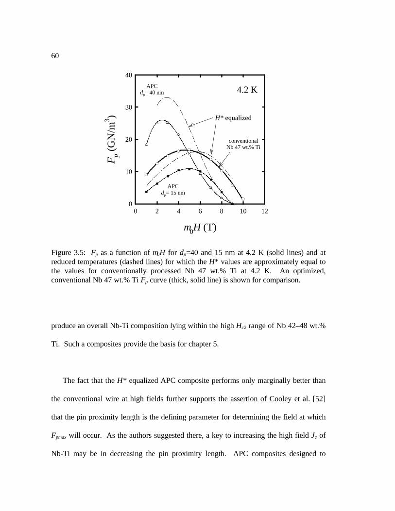
60
produce an overall Nb-Ti composition lying within the high Hc2 range of Nb 42–48 wt.%
Ti. Such a composites provide the basis for chapter 5.
The fact that the H* equalized APC composite performs only marginally better than
the conventional wire at high fields further supports the assertion of Cooley et al. [52]
that the pin proximity length is the defining parameter for determining the field at which
Fpmax will occur. As the authors suggested there, a key to increasing the high field Jc of
Nb-Ti may be in decreasing the pin proximity length. APC composites designed to
µ0H (T)
0 2 4 6 8 10 12
Fp
(GN
/m3 )
0
10
20
30
40
H* equalized
4.2 KAPCdp= 40 nm
APCdp= 15 nm
conventionalNb 47 wt.% Ti
Figure 3.5: Fp as a function of µ0H for dp=40 and 15 nm at 4.2 K (solid lines) and atreduced temperatures (dashed lines) for which the H* values are approximately equal tothe values for conventionally processed Nb 47 wt.% Ti at 4.2 K. An optimized,conventional Nb 47 wt.% Ti Fp curve (thick, solid line) is shown for comparison.

61
improve the high field pinning through decreases in the pin proximity length are the basis
for chapter 6.
3.4 Conclusions
The microstructure and superconducting properties Jc, Fp, and H* have been studied for
an APC composite consisting of Nb 47 wt.% Ti with 24 vol.% of Nb pinning centers. A
maximum bulk flux pinning force of 25 GN/m3 occurred at ~0.25Hc2 when the nominal
pin diameter was 40 nm. However, the actual pinning center thickness at this size
ranged from <1 to 16 nm. As the pin size was further reduced, the Fp peak position
shifted to higher fields, and the peak magnitude decreased. Over this entire range of
(dp=165–15 nm) the irreversibility field decreased from 10.3 to 9 T. All of these trends
are qualitatively consistent with Nb-pin APC composites of similar compositions,
fabricated by other groups using different methods.
By reducing the temperature at which the APC wires were measured, the values of
H* were equalized to the value of 10.3 T for optimized, conventional Nb 47 wt.% Ti in
order to compensate for the non-optimal composition of the matrix and pin mixture. At
fields up to 7 T, the APC composite clearly outperformed the conventional wire,
achieving a Jc(5 T) of 4600 A/mm2 when H* was equalized.
The Jc properties of these initial APC composites compare favorably to other Nb-pin
composites of similar design by Matsumoto et al. [31], Motowidlo et al. [27], and
Cooley [29], thus demonstrating our rod-based process to be a viable method for
fabricating APC wires. However, a significant difference in Jc(dp, H) behavior between
62
composites which received three or four warm extrusions suggests that the fourth
extrusion produced a marked effect on the flux pinning nanostructure, most likely by
diminishing the strength of the pinning wells through pin/matrix interdiffusion. This issue
is further addressed in the next chapter.

63
4. Improved thermomechanical processing
While the thermomechanical processing steps [20, 21] and the resulting flux pinning
nanostructures [21, 22, 23] of high-Jc conventional Nb-Ti wire are firmly established,
the same is not true for APC wires. Consequently, it is not surprising that a significant
range in Jc(H) is found for APC composites of nominally the same composition but
manufactured via different processing routes. For instance, two groups have
manufactured and characterized APC composites of similar content to the composite
described in chapter 3, namely, Nb 47 wt.% Ti with 24–25 vol.% of nominally round
[91] or planar [33] Nb pins. These composites produced maximum Jc(5 T) values of
3200, 2400 and 2800 A/mm2, respectively. Although hard evidence is lacking, it seems
likely that the range in Jc originates from differences in the flux pinning nanostructures.
As recent work by Jablonski, Lee, and Larbalestier [39] has shown, the detailed
64
nanostructure of the pins exerts an important effect on the attainable Jc, independent of
the volume fraction of pin and its composition.
A very important difference between conventional and APC Nb-Ti lies in the
evolution of the flux pinning nanostructures during processing. Conventionally
processed Nb-Ti alloy becomes two phase late in its processing and only room-
temperature wire drawing is necessary to reduce the α-Ti precipitate down to optimum
flux pinning thickness (1–2 nm). APC wires, on the other hand, are two-phase
throughout their fabrication and some elevated temperature processing is generally
unavoidable. All practical APC composites require 1–4 warm extrusion steps, usually
oC. Interdiffusion associated with elevated temperature
processing can mix the pin and matrix materials, weakening the sharpness of the
designed two-phase nanostructure.
Our previous study [54] described in chapter 3 and a study by Kanithi et al. [92]
showed that the ultimate Jc(H) behavior of APC wires containing Nb 47 wt.% Ti with Nb
pins was very sensitive to the number of warm (~600 oC) extrusions used in their
fabrication. In our study, for the same nominal pin diameter, a wire which had received
three 650 oC extrusions exhibited dramatically different Jc(H) behavior compared to that
for a wire which had received a fourth extrusion, as shown in Figure 3.2. Below 4 T the
three-extrusion wire had higher critical current densities, while above 5 T the reverse was
seen. As we could detect no difference in the average pin thickness or the pin thickness
distribution at the optimum flux pinning size (dp=40 nm) for either composite, we

65
attributed the difference in behavior to pin/matrix interdiffusion caused by the fourth
extrusion. Since interdiffusion should reduce the pin proximity length by alloying the Nb,
this should lead to the elementary pinning force reaching its peak for thinner pins [52],
thus raising the density of pins at maximum fp, and enhancing the bulk pinning force at
higher fields where higher Jc is most desirable. However, such interdiffusion should also
diminish the composition gradient at the pin/matrix interface, thereby decreasing the
strength of fp. Thus interdiffusion can have two opposing effects, making the quantitative
impact on Jc unpredictable.
4.1 Experimental design
In order to directly address the influence of the sharpness of the pinning well on the
strength of fp, we fabricated a new, nominally identical Nb 47 wt.% Ti/Nb APC
composite but this time using lower temperature processing. We reduced the number of
warm extrusions from four to three and the temperature of the last extrusion from 650 oC
to 250 oC. The composite was fabricated using the rod-based technique. Table 4.1
summarizes the fabrication details for this composite. Thirty-one 1 mm diameter rods of
Nb were arranged in a hexagonal array within 96 rods of Nb 47 wt.% Ti, such that the
center-to-center pin spacing was 1.82dp. The hexagonal-shaped 127 rod stack was
canned in Cu, evacuated and hydrostatically warm extruded at 650 oC using a 15:1 area
reduction ratio. The extruded wire was cut into 127 filaments, the Cu was etched off and
the hexagonal-shaped filaments were re-stacked, canned in Cu and extruded under the
same conditions. A third stack of 55 filaments was extruded at 250 oC using a 10:1
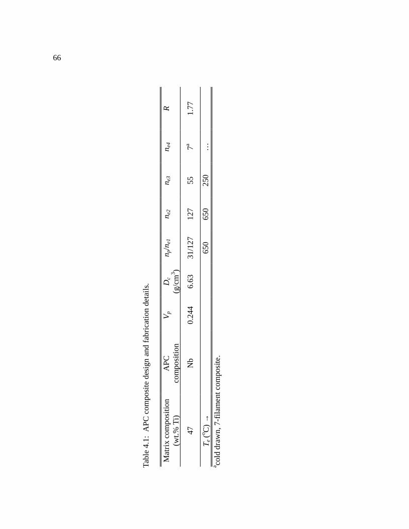
66
Tabl
e 4.
1: A
PC
com
posi
te d
esig
n an
d fa
bric
atio
n de
tail
s.
Mat
rix
com
posi
tion
(wt.%
Ti)
AP
Cco
mpo
siti
onV
pD
c
(g/c
m3 )
n p/n
e1n e
2n e
3n e
4R
47N
b0.
244
6.63
31/1
2712
755
7a1.
77
Te (
o C)
→65
065
025
0…
a cold
dra
wn,
7-f
ilam
ent c
ompo
site
.

67
area reduction ratio. This final warm extrusion brought the nominal pin diameter down
to 1.3 µm. The resulting wire was re-stacked with the Cu left on so as to produce a wire
with seven superconducting filaments, each filament containing 31×127×55 pinning
centers. This wire was drawn to various sizes down to 0.08 mm diameter.
4.2 Results
Figure 4.1(a) shows a transverse cross-section of the APC wire at dp=400 nm. Each
of the seven superconducting filaments shown contains 216,535 Nb pinning centers,
several of which are shown in the accompanying field-emission scanning electron
micrograph (secondary electron image) of Figure 4.1(b). The contrast between the Nb
and Nb 47 wt.% Ti was obtained by lightly etching with a mixture of 25% HNO3, 25%
HF and 50% H2O. At this size, the nominally round pins have started to deform into
ribbons but the designed hexagonal symmetry of the pinning center array is still evident.
The transmission electron micrograph of Figure 4.1(c) reveals that by dp=25 nm (slightly
smaller than the optimum flux pinning size of dp=39 nm) the round pins have transformed
into ribbons whose thickness ranges rather broadly from ~1 to 15 nm. This ribbon-shape
range parallels that observed in the earlier composite of chapter 3.
Figure 4.2 shows Jc as a function of the nominal pin diameter at applied magnetic
fields of 2–7 T for the two prior composites having three and four extrusions respectively
and for the new three-extrusion composite. The new composite achieves significantly
larger values of Jc. Progressive peaks in Jc(dp) can be seen at 42, 35, 29, 25
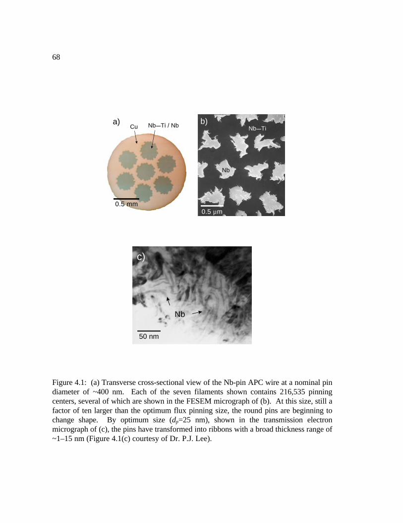
68
0.5 mm0.5 µm
Cu Nb—Ti / Nb
Nb
Nb—Tia) b)
c)
Nb
50 nm
Figure 4.1: (a) Transverse cross-sectional view of the Nb-pin APC wire at a nominal pindiameter of ~400 nm. Each of the seven filaments shown contains 216,535 pinningcenters, several of which are shown in the FESEM micrograph of (b). At this size, still afactor of ten larger than the optimum flux pinning size, the round pins are beginning tochange shape. By optimum size (dp=25 nm), shown in the transmission electronmicrograph of (c), the pins have transformed into ribbons with a broad thickness range of~1–15 nm (Figure 4.1(c) courtesy of Dr. P.J. Lee).
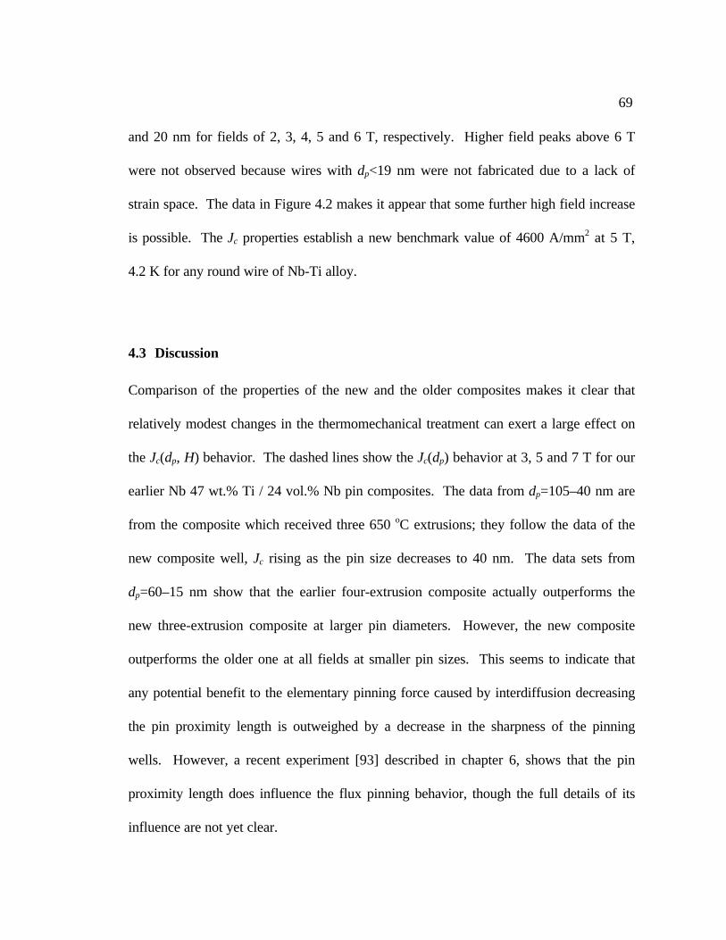
69
and 20 nm for fields of 2, 3, 4, 5 and 6 T, respectively. Higher field peaks above 6 T
were not observed because wires with dp<19 nm were not fabricated due to a lack of
strain space. The data in Figure 4.2 makes it appear that some further high field increase
is possible. The Jc properties establish a new benchmark value of 4600 A/mm2 at 5 T,
4.2 K for any round wire of Nb-Ti alloy.
4.3 Discussion
Comparison of the properties of the new and the older composites makes it clear that
relatively modest changes in the thermomechanical treatment can exert a large effect on
the Jc(dp, H) behavior. The dashed lines show the Jc(dp) behavior at 3, 5 and 7 T for our
earlier Nb 47 wt.% Ti / 24 vol.% Nb pin composites. The data from dp=105–40 nm are
from the composite which received three 650 oC extrusions; they follow the data of the
new composite well, Jc rising as the pin size decreases to 40 nm. The data sets from
dp=60–15 nm show that the earlier four-extrusion composite actually outperforms the
new three-extrusion composite at larger pin diameters. However, the new composite
outperforms the older one at all fields at smaller pin sizes. This seems to indicate that
any potential benefit to the elementary pinning force caused by interdiffusion decreasing
the pin proximity length is outweighed by a decrease in the sharpness of the pinning
wells. However, a recent experiment [93] described in chapter 6, shows that the pin
proximity length does influence the flux pinning behavior, though the full details of its
influence are not yet clear.
70
dp (nm)
0 20 40 60 80 100
J c (A
/mm
2 )
0
5000
10000
150002 T
3 T
4 T
7 T
6 T
5 T
4.2 K
5 T
3 T
7 T
Figure 4.2: Jc as a function of dp at applied fields from 2–7 T for the Nb-pin APCcomposites at 4.2 K. The filled symbols connected by continuous lines represent thepresent composite for which the last extrusion temperature was reduced. The smallersymbols connected by dashed lines are Jc(dp) data at 3, 5 and 7 T taken from theprevious composite which had the same composition of Nb 47 wt.% Ti with 24 vol.%Nb pins, but had received higher temperature processing. Two data sets are shown, thatfrom dp=105–40 nm (open symbols) corresponds to a third extrusion composite, whilethat from dp=60–15 nm (crossed symbols) corresponds to a fourth extrusion composite.
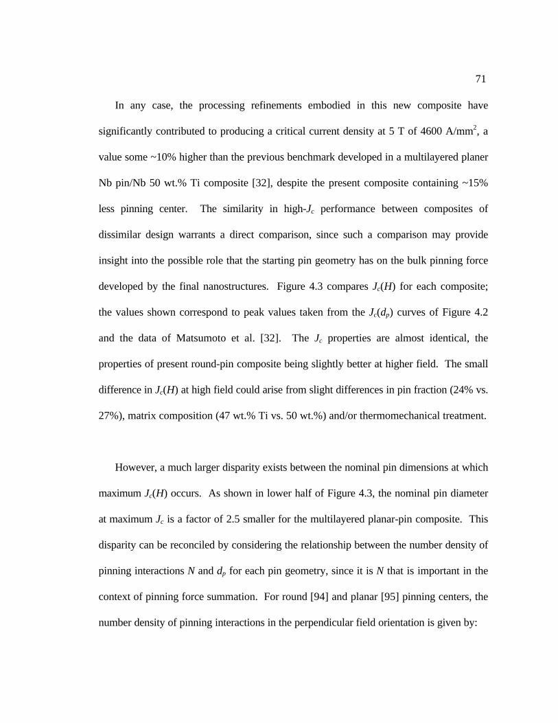
71
In any case, the processing refinements embodied in this new composite have
significantly contributed to producing a critical current density at 5 T of 4600 A/mm2, a
value some ~10% higher than the previous benchmark developed in a multilayered planer
Nb pin/Nb 50 wt.% Ti composite [32], despite the present composite containing ~15%
less pinning center. The similarity in high-Jc performance between composites of
dissimilar design warrants a direct comparison, since such a comparison may provide
insight into the possible role that the starting pin geometry has on the bulk pinning force
developed by the final nanostructures. Figure 4.3 compares Jc(H) for each composite;
the values shown correspond to peak values taken from the Jc(dp) curves of Figure 4.2
and the data of Matsumoto et al. [32]. The Jc properties are almost identical, the
properties of present round-pin composite being slightly better at higher field. The small
difference in Jc(H) at high field could arise from slight differences in pin fraction (24% vs.
27%), matrix composition (47 wt.% Ti vs. 50 wt.%) and/or thermomechanical treatment.
However, a much larger disparity exists between the nominal pin dimensions at which
maximum Jc(H) occurs. As shown in lower half of Figure 4.3, the nominal pin diameter
at maximum Jc is a factor of 2.5 smaller for the multilayered planar-pin composite. This
disparity can be reconciled by considering the relationship between the number density of
pinning interactions N and dp for each pin geometry, since it is N that is important in the
context of pinning force summation. For round [94] and planar [95] pinning centers, the
number density of pinning interactions in the perpendicular field orientation is given by:

72
N d as≅ 1 02( ) ( )d as ≤ 0 (4.1)
where ds is the pin spacing. Thus it is ds rather than dp that determines N. For 24 vol.%
of round pins the average pin spacing ds :
d d V ds p p p≈ =12 142 . (4.2a)
while for 27 vol.% of planar pins,
d d V ds p p p≈ = 37. (4.2b)
This analysis shows that for a given pin dimension dp, ds is approximately 2.6 times larger
for the planar pin array; this difference accounts for the entire offset in dpmax between the
two composites.
Since the real pin morphology deviated substantially from design as the size
approached nanometer dimensions [Figure 4.1(c)], the above analysis is appropriate for
discussing only relative differences in the pin density between the two APC designs.
Implicit in this analysis is that the pin shape transformed from regular to ribbon-in the
same manner for both designs. This is a valid assumption since both composites received
similar axially symmetric deformation processing. Determination of the real pin density
requires detailed measurement of the final size microstructure, such as that performed by
Meingast, Lee and Larbalestier for optimized, conventional Nb 48 wt.% Ti [23]. Such a
detailed quantitative analysis was not possible in this study.
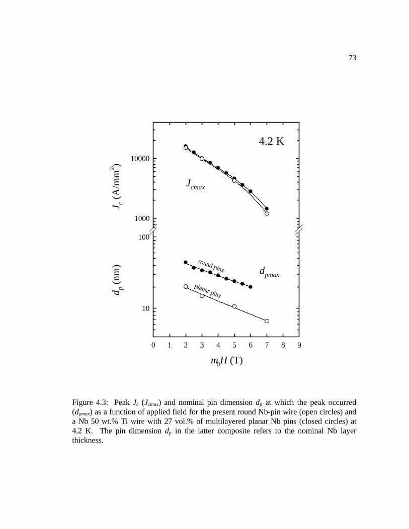
73
µ0H (T)
0 1 2 3 4 5 6 7 8 9
d p (n
m)
J c
(A/m
m2 )
10
100
1000
10000
Jcmax
dpmax
4.2 K
planar pins
round pins
Figure 4.3: Peak Jc (Jcmax) and nominal pin dimension dp at which the peak occurred(dpmax) as a function of applied field for the present round Nb-pin wire (open circles) anda Nb 50 wt.% Ti wire with 27 vol.% of multilayered planar Nb pins (closed circles) at4.2 K. The pin dimension dp in the latter composite refers to the nominal Nb layerthickness.

74
The final shape and thickness distribution of the pins is likely to be very important in
determining the flux pinning properties because of the influence that these parameters
exert on the proximity coupling of the pins to the matrix. Round Nb pins change shape
drastically in ways dictated by the deformation characteristics and the grain structures of
the pin and matrix materials. Even with the additional processing refinements of this
study, the pin thickness at optimum size varied from ~1–15 nm, a broader range than is
observed in conventional Nb-Ti. Broad pin thickness distributions, such as those found
in PMAPC wires with Nb pins [39] and inhomogeneous conventionally processed Nb-Ti
[96], are believed to be detrimental to Jc. Thus further significant increases in Jc should
be possible from more uniform artificial pinning structures, as is suggested by recent
multilayer studies by McCambridge et al. [97] and Kadyrov, Gurevich, and Larbalestier
[98].
It is important to note that the Jc improvements in the new Nb-pin composite were
realized in the absence of any added improvement to H*. At the maximum Jc(5 T) size
(dp=25 nm), H* determined by both magnetization and extrapolation of Fp→0 was ~9.2
T, essentially the same value as that interpolated from the data of Table 3.2 for our
previous round Nb-pin composite. Thus applying a similar normalization correction to Jc
of ~45% to the present composite yields Jc(5 T, µ0H*=10.7 T)=6600 A/mm2. This value
is 80% higher than the best conventionally processed Nb-Ti wire. Clearly there is every
incentive to maximize H*, Hc2 by designing the overall Nb-pin/Nb-Ti for maximum Hc2,
75
in accordance with the hypothesis of Meingast, Lee, and Larbalestier [23]. Such an
experiment provides the basis for chapter 5.
4.4 Conclusions
The critical current density of Nb 47 wt.% Ti wires with 24 vol.% of nominally round
artificial Nb pinning centers were studied as a function of pin diameter and magnetic
field. Very high Jc values were obtained when interdiffusion between pin and matrix was
minimized by using lower temperature thermomechanical processing. A high Jc(5 T, 4.2
K) for round wire of 4600 A/mm2 was achieved for a nominal pin diameter of 25 nm,
despite the absence of any added improvement to the irreversibility field. Transmission
electron microscopy showed that the real pin shape was ribbon-like with a thickness
which varied from ~1–15 nm.

76
77
5. Effect of Nb-Ti matrix composition
This chapter discusses APC composites designed to address the depressed Hc2 and H*
values observed in our previous APC composites composed of Nb 47 wt.% Ti with 24
vol.% Nb pins. As shown in chapter 4, Jc was increased by ~40% in wires with pure Nb
pins through only modest changes in the thermomechanical treatment. These
improvements were realized in the absence of any added improvement to H* or Hc2.
Since Jc generally scales with Hc2 and it is the higher-field Jc that is of greatest interest
for high energy physics projects, there is every incentive to attain the highest possible Hc2
in this system ~11.7 T for Nb 44 wt.% Ti [100].
A study of conventionally processed Nb 47 wt.% Ti wire during its final optimization
strain by Meingast, Lee, and Larbalestier [23] explained a simultaneous decrease in Tc
and increase in Hc2 as a kind of electromagnetic “homogenization” as the α-Ti precipitate
thickness was reduced below ξ. Their hypothesis explains the depressed Hc2 found in
78
Nb-pin composites as resulting from an overall composite mixture which departs from
Nb 44–48 wt.% Ti, the range of composition for which maximum Hc2 occurs. Thus the
goal of this study was to test the hypothesis for Nb-pin APC composites designed for
optimum Hc2 in the coupled limit.
5.1 Experimental design
Two APC wires with 24 vol.% Nb pins were fabricated according to the exact
specifications given for the Nb 47 wt.% Ti/Nb composite described in chapter 4, a
singular difference being the selection of more Ti-rich matrix compositions in order to
shift the overall Nb-Ti/Nb composition closer to Nb 44 wt.% Ti in the fully proximity-
effect coupled limit. For this purpose, Nb 52 wt.% Ti and Nb 62 wt.% Ti were chosen
based on the availability of high homogeneity, low impurity concentration alloy rods
custom made for the thesis study of McKinnell [77]. Nb-Ti /Nb overall compositions
(OC) in wt.% Ti were calculated using:
OC MC=−
+ −
D V
D V D Vm p
p p m p
( )
( )
1
1, (5.1)
where MC is the Nb-Ti composition in wt.% Ti, and Dp and Dm are the mass densities of
the pin and Nb-Ti matrix, respectively. Values of Dp, Vp, OC, and Hc2 for each overall
composition, as measured by magnetization [100], are listed in Table 5.1 for each
composite. As shown in Table 5.1, Nb 52 and 62 wt.% Ti with 24 vol.% Nb correspond
to overall compositions of 35 and 42 wt.% Ti, respectively, and thus, in the fully coupled

79
limit, should develop significantly higher Hc2 than the previous Nb-pin composite design.
Table 5.2 summarizes the fabrication details for this set of composites.
Hc2 and H* were measured only for the Nb 47 and 62 wt.% Ti 7-filament composites.
During the course of magnetization measurement on the present sample set, we
discovered that our previous analysis of M(H) for APC wires, discussed in chapter 3, had
incorrectly defined a measurement artifact associated with a small axial offset of the
sample position with respect to the Helmholtz coil pair as H*. In turn, H* had been
incorrectly defined as Hc2. Exacerbating this problem was that the real Hc2 transition,
characterized by a minute increase in the slope of the reversible magnetization, was
seldom discernible above the background noise. In the present study, the difficulty in
measuring Hc2 was alleviated by increasing the sample volume, and hence the moment,
by a factor of ~5 in order to better resolve the Hc2 transition. The Cu matrix was
chemically removed in order to increase the superconductor fill factor and also to
remove a small temperature-dependent diamagnetic contribution from the copper. As in
our previous magnetization study, the sample length was maximized
Table 5.1: Composite density, overall composition (OC), and Hc2 values.
Matrix composition(wt.% Ti)
Vp Dm
(g/cm3)Dc
(g/cm3)OC
(wt.% Ti)µ0Hc2
[100](T)
47 0.244 6.02 6.63 33 10.4
52 0.244 5.77 6.44 35 10.6
62 0.244 5.52 6.25 42 11.6
80
in order to insure that the magnetization correlated to Jc flowing parallel to the pins (Jc||)
rather than Jc crossing the pins at each end of the wire (Jc⊥). Small (<0.3 mm) diameter
wires were wound into 3 mm diameter, 2 mm tall open-circuit coils encased in Duco
cement. However, this geometry was not feasible for the two largest diameter wires (1
and 0.3 mm dia.). Fortunately, these large-diameter wires had correspondingly large-
diameter pins and thus low pin densities, low Jct, and low Jc||/ Jc⊥ anisotropy. In every
case where Jcm could be compared to Jct, there was close agreement, thus providing a
strong indication that the longitudinal critical current density, corresponding to Jct,
determined ∆M and thus H*.
5.2 Results
Figures 5.1(a)–(c) plot the bulk pinning force Fp(H) curves as a function of the nominal
pin diameter for the Nb 47, 52, and 62 wt % Ti-matrix Nb-pin composites, respectively.
One similarity between the three composites is the absence of low field data for the
larger pin wires. This is a consequence of having wires with high-Jc and rather large
diameter (>50 µm) filaments, a combination which caused flux jumping [56] to the
normal state at transport currents well below Ic. Flux jumping was suppressed as the
wire diameter was further reduced.
A second similarity between the three composites is shown by their qualitatively similar
Fp(H) development with decreasing pin diameter. As dp was reduced below 100 nm, a
low-field peak in Fp(H) emerged, while the magnitude of Fp increased at all
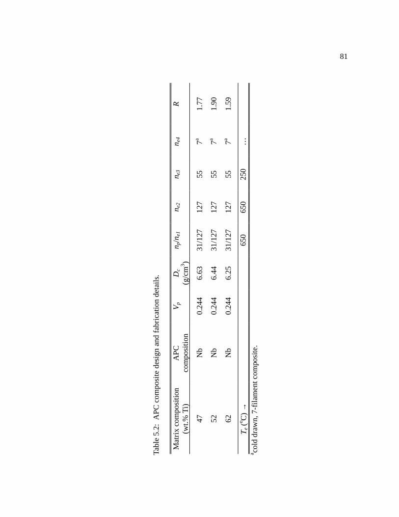
81
Tabl
e 5.
2: A
PC
com
posi
te d
esig
n an
d fa
bric
atio
n de
tail
s.
Mat
rix
com
posi
tion
(wt.%
Ti)
AP
Cco
mpo
siti
onV
pD
c
(g/c
m3 )
n p/n
e1n e
2n e
3n e
4R
47N
b0.
244
6.63
31/1
2712
755
7a1.
77
52N
b0.
244
6.44
31/1
2712
755
7a1.
90
62N
b0.
244
6.25
31/1
2712
755
7a1.
59
Te (
o C)
→65
065
025
0…
a cold
dra
wn,
7-f
ilam
ent c
ompo
site
.
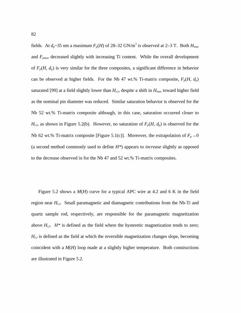
82
fields. At dp~35 nm a maximum Fp(H) of 28–32 GN/m3 is observed at 2–3 T. Both Hmax
and Fpmax decreased slightly with increasing Ti content. While the overall development
of Fp(H, dp) is very similar for the three composites, a significant difference in behavior
can be observed at higher fields. For the Nb 47 wt.% Ti-matrix composite, Fp(H, dp)
saturated [99] at a field slightly lower than Hc2, despite a shift in Hmax toward higher field
as the nominal pin diameter was reduced. Similar saturation behavior is observed for the
Nb 52 wt.% Ti-matrix composite although, in this case, saturation occurred closer to
Hc2, as shown in Figure 5.2(b). However, no saturation of Fp(H, dp) is observed for the
Nb 62 wt.% Ti-matrix composite [Figure 5.1(c)]. Moreover, the extrapolation of Fp→0
(a second method commonly used to define H*) appears to increase slightly as opposed
to the decrease observed in for the Nb 47 and 52 wt.% Ti-matrix composites.
Figure 5.2 shows a M(H) curve for a typical APC wire at 4.2 and 6 K in the field
region near Hc2. Small paramagnetic and diamagnetic contributions from the Nb-Ti and
quartz sample rod, respectively, are responsible for the paramagnetic magnetization
above Hc2. H* is defined as the field where the hysteretic magnetization tends to zero;
Hc2 is defined as the field at which the reversible magnetization changes slope, becoming
coincident with a M(H) loop made at a slightly higher temperature. Both constructions
are illustrated in Figure 5.2.
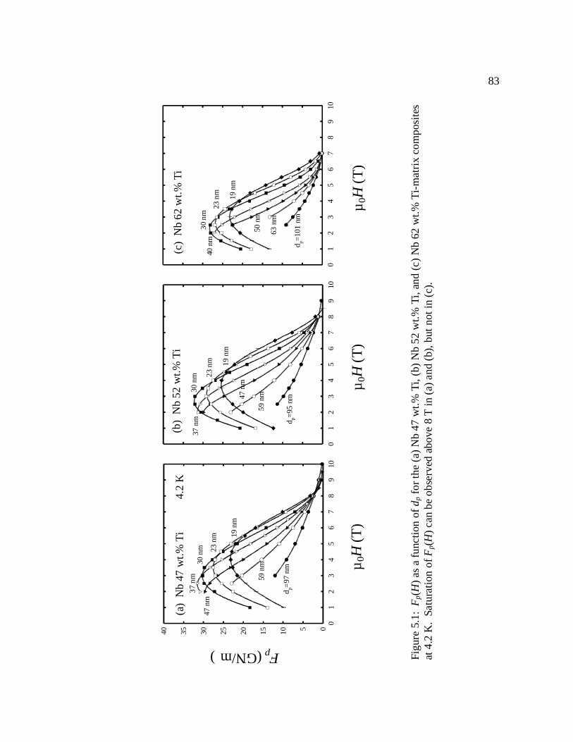
83
01
23
45
67
89
100510152025303540
(a)
Nb
47 w
t.% T
i
d p=97
nm
59 n
m
47 n
m
37 n
m30
nm 23
nm 19
nm
4.2
K
01
23
45
67
89
10
(c)
Nb
62 w
t.% T
i
d p=10
1 nm
63 n
m
50 n
m
40 n
m30
nm
23 n
m 19 n
m
01
23
45
67
89
10
(b)
Nb
52 w
t.% T
i
d p=95
nm
19 n
m
23 n
m
30 n
m
59 n
m47 n
m
37 n
m
Fp (GN/m)
µ 0H
(T
)µ 0
H (
T)
µ 0H
(T
)
Figu
re 5
.1:
Fp(
H)
as a
fun
ctio
n of
dp
for
the
(a)
Nb
47 w
t.% T
i, (b
) N
b 52
wt.%
Ti,
and
(c)
Nb
62 w
t.% T
i-m
atri
x co
mpo
site
sat
4.2
K.
Satu
rati
on o
f Fp(
H)
can
be o
bser
ved
abov
e 8
T in
(a)
and
(b)
, but
not
in (
c).
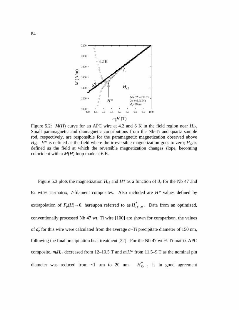
84
Figure 5.3 plots the magnetization Hc2 and H* as a function of dp for the Nb 47 and
62 wt.% Ti-matrix, 7-filament composites. Also included are H* values defined by
extrapolation of Fp(H)→0, hereupon referred to as HFp→0* . Data from an optimized,
conventionally processed Nb 47 wt. Ti wire [100] are shown for comparison, the values
of dp for this wire were calculated from the average α-Ti precipitate diameter of 150 nm,
following the final precipitation heat treatment [22]. For the Nb 47 wt.% Ti-matrix APC
composite, µ0Hc2 decreased from 12–10.5 T and µ0H* from 11.5–9 T as the nominal pin
diameter was reduced from ~1 µm to 20 nm. HFp→0* is in good agreement
µ0H (T)
6.0 6.5 7.0 7.5 8.0 8.5 9.0 9.5 10.0
M (
A/m
)
1000
1200
1400
1600
1800
2000
2200
4.2 K
6 K Hc2
H*Nb 62 wt.% Ti24 vol.% Nbdp=80 nm
Figure 5.2: M(H) curve for an APC wire at 4.2 and 6 K in the field region near Hc2.Small paramagnetic and diamagnetic contributions from the Nb-Ti and quartz samplerod, respectively, are responsible for the paramagnetic magnetization observed aboveHc2. H* is defined as the field where the irreversible magnetization goes to zero; Hc2 isdefined as the field at which the reversible magnetization changes slope, becomingcoincident with a M(H) loop made at 6 K.
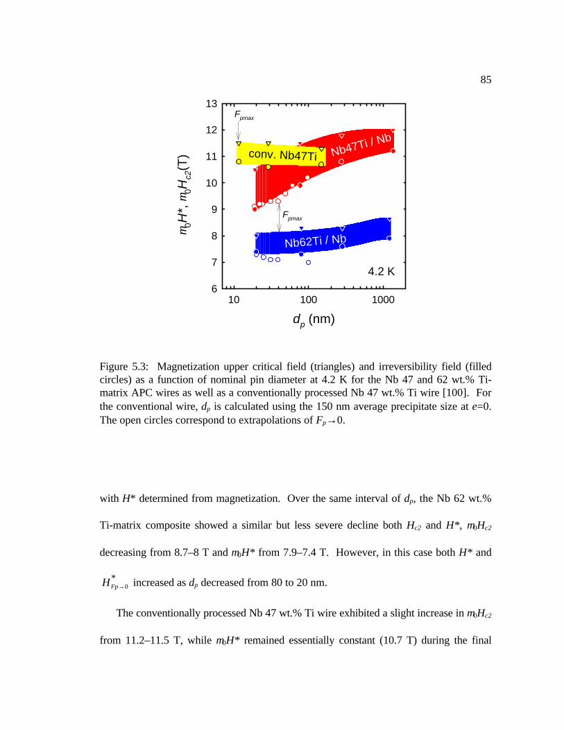
85
with H* determined from magnetization. Over the same interval of dp, the Nb 62 wt.%
Ti-matrix composite showed a similar but less severe decline both Hc2 and H*, µ0Hc2
decreasing from 8.7–8 T and µ0H* from 7.9–7.4 T. However, in this case both H* and
HFp→0* increased as dp decreased from 80 to 20 nm.
The conventionally processed Nb 47 wt.% Ti wire exhibited a slight increase in µ0Hc2
from 11.2–11.5 T, while µ0H* remained essentially constant (10.7 T) during the final
dp (nm)
10 100 1000
µ0H
*, µ
0Hc2
(T)
6
7
8
9
10
11
12
13
Fpmax
Nb62Ti / Nb
Nb47Ti / Nbconv. Nb47Ti
Fpmax
4.2 K
Figure 5.3: Magnetization upper critical field (triangles) and irreversibility field (filledcircles) as a function of nominal pin diameter at 4.2 K for the Nb 47 and 62 wt.% Ti-matrix APC wires as well as a conventionally processed Nb 47 wt.% Ti wire [100]. Forthe conventional wire, dp is calculated using the 150 nm average precipitate size at ε=0.The open circles correspond to extrapolations of Fp→0.

86
optimization strain, corresponding to a decrease in dp from 150–10 nm. The vertical
arrows in Figure 5.3 indicate the nominal pin diameters at which each composite reached
their maximum value of Fp (Fpmax). Fpmax occurred at dp~40 nm for both Nb-pin
composites while for the conventional wire Fpmax occurred at dp~10 nm; the actual pin
thickness at these sizes ranged from ~1–20 nm and 1–5 nm, respectively.
5.3 Discussion
5.3.1 Microstructural development
Although no electron microscopy is presented for the Nb 52 and 62 wt.% Ti-matrix
composites, their pin arrays were observed by FESEM at intermediate pin diameters of
~500 and 100 nm. The degradation in pin shape appeared to proceed in identical fashion
to that for the Nb 47 wt.% Ti composite, as shown in Figure 4.1(b) and a similar trend
was expected down to the optimum flux pinning range of dp=100–20 nm. This is a
reasonable assumption, since any deviation in the pin shape from that of the Nb 47 wt.%
Ti-matrix composite should have commenced at a much earlier stage in processing. It
should be noted that ~1–3 volume percent of equiaxed α-Ti precipitate was observed in
FESEM performed on the Nb 62 wt.% Ti-matrix composite following its last extrusion;
no precipitation was detected in the Nb 47 and 52 wt.% Ti-matrix composites. This is
not surprising since the nucleation and growth kinetics for α-Ti precipitation increase
rapidly with increasing Ti content. However the precipitate diameter of 30–50 nm was
~50 times smaller than the pin diameter at this size, and thus were inconsequential to the
87
Fp(H) curves of Figure 5.1(c). Therefore, all further discussion of the Nb 47, 52 and 62
wt.% Ti-matrix composites will assume nanostructural consistency.
5.3.2 H* and Hc2 vs. dp
Taken together, Figures 5.1 and 5.3 clearly show the trends in H* and Hc2 with
decreasing dp. For the Nb 47 wt.% Ti-matrix composite, the Nb pins appear to be fully
coupled to the matrix by dp=20 nm: the µ0Hc2 of 10.4 T is equal to the value given in
Table 5.1 for the overall composite mixture of Nb 33 wt.% Ti. However the Nb 62
wt.% Ti-matrix composite only developed Hc2=8 T by dp=20 nm, well below the value of
11.6 T predicted in the fully coupled limit.
In light of this somewhat surprising result, two additional containing Nb 47 and 62
wt.% Ti-matrix composites were fabricated to explore further changes in H* and Hc2 at
finer pin diameters than the 7-filament architecture allowed. The new wires were
fabricated from the same monofilamentary stock used for the 7-filament conductors, the
only difference being that 55-filament wires were made by low (250oC) temperature
extrusion rather than cold drawing. Whereas the 7-filament composites provided a final
nominal pin diameter of 19 nm, the 55-filament composites provided dp=7 nm.
Extrapolation of pin thickness measurements made at dp~25 nm [Figure 4.1(c)] down to
dp=7 nm, yields a thickness range of <<1–2 nm, well below the 5 and 6 nm coherence
lengths of Nb 47 and 62 wt.% Ti, respectively.
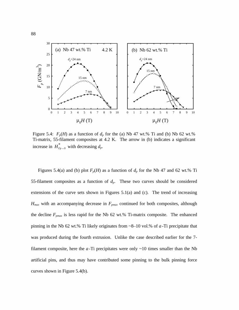
88
Figures 5.4(a) and (b) plot Fp(H) as a function of dp for the Nb 47 and 62 wt.% Ti
55-filament composites as a function of dp. These two curves should be considered
extensions of the curve sets shown in Figures 5.1(a) and (c). The trend of increasing
Hmax with an accompanying decrease in Fpmax continued for both composites, although
the decline Fpmax is less rapid for the Nb 62 wt.% Ti-matrix composite. The enhanced
pinning in the Nb 62 wt.% Ti likely originates from ~8–10 vol.% of α-Ti precipitate that
was produced during the fourth extrusion. Unlike the case described earlier for the 7-
filament composite, here the α-Ti precipitates were only ~10 times smaller than the Nb
artificial pins, and thus may have contributed some pinning to the bulk pinning force
curves shown in Figure 5.4(b).
µ0H (T)
0 1 2 3 4 5 6 7 8 9 10
µ0H (T)
0 1 2 3 4 5 6 7 8 9 10
Fp
(GN
/m3 )
0
5
10
15
20
25
30
(b) Nb 62 wt.% Ti(a) Nb 47 wt.% Ti
15 nm
7 nm7 nm
15 nm
dp=24 nm
4.2 K
dp=24 nm
Figure 5.4: Fp(H) as a function of dp for the (a) Nb 47 wt.% Ti and (b) Nb 62 wt.%Ti-matrix, 55-filament composites at 4.2 K. The arrow in (b) indicates a significant
increase in HFp→0* with decreasing dp.
89
Examination of Fp(H) near Hc2 for the Nb 47 wt.% Ti-matrix composite shows
saturation of Fp(H) above 8 T and HFp→0* ~9 T, exactly the behavior observed in Figure
5.1(a) as dp approached 19 nm and further validation that the pins are fully coupled to
the matrix. For the Nb 62 wt.% Ti-matrix composite, HFp→0* increased from 7.5 to 8.7
T as dp decreased from 24 to 7 nm. Although the 1.2 T enhancement in H* is significant,
it is still 3 T lower than the predicted µ0Hc2 of 11.6 T. In light of the discrepancy
between the behavior expected from the phenomenological predictions of Meingast, Lee,
and Larbalestier, and the behavior observed for the Nb-pin wires, an analysis of
proximity effect theory is necessary.
5.3.3 Proximity effect theory
Proximity-effect theory [42, 43, 45, 46] describes the behavior of dirty-superconductor–
normal-metal (S/N) bilayers as the bilayer period approaches the coherence length ξ.
Microscopically the proximity effect involves diffusion of superelectrons from the
superconductor into the normal metal. A decrease in the layer thicknesses is generally
accompanied by a decrease in Tc and/or Hc2, the magnitude of which is dictated by the
respective layer thicknesses and proximity lengths. In the context of traditional
proximity-effect theory, no increase in Tc or Hc2 is considered.
However, in the Nb-Ti system, as well as other superconducting alloy systems such
as Nb-Zr and Nb-Ta, the alloy is a stronger superconductor than the pure element
constituents. Thus in the limit of infinitesimal bilayer period, the superconducting
90
properties should approach the higher properties of the homogenous mixture. This has
been observed experimentally in studies of pure Nb/Ti thin film multilayers by Sato
[101], Qian et al. [102], and Warnes, Faase, and Norris [103, 104]. In each of these
cases, traditional proximity effect theory fails to properly describe the superconducting
properties in the limit of infinitesimal layer thicknesses. In order to address this obvious
shortcoming of traditional proximity-effect theory Ledvij, Dobrosavljevij-Grujic, and
Clem [105] developed a trilayer model to describe the behavior of Nb/Ti multilayer films
with decreasing layer thickness. They modeled the Nb/Ti films as superconductor-
interphase-normal-metal (S/I/N) multilayers, for which the alloy Nb-Ti interphase layer
accounts for interfacial roughness or mixing of Nb and Ti due to interdiffusion. As the
trilayer period decreases, the interphase Nb-Ti layer accounts for an increasingly large
fraction of the trilayer, dominating the behavior at infinitesimal bilayer periods. This
model accurately described the initial decrease and then subsequent increase in Tc for the
Nb/Ti multilayers of Qian et al. [102] as the bilayer period was reduced from 200 to 1
nm.
Thus, a fundamental difference exists between the phenomenological proximity
“mixing” model proposed by Meingast, Lee, and Larbalestier and the trilayer proximity-
effect model developed by Levij et al. Within the framework of the former model, the
coherence length is the characteristic length scale which governs the Tc and Hc2 in the
fully coupled limit, while in the latter model, the volume fraction of interphase layer
determines the properties. It appears that the latter model more accurately describes the

91
properties of the Nb 62 wt.% Ti-matrix composite. Since the thermomechanical
processing in the present composites were tailored to minimize pin-matrix interdiffusion,
the interphase layer should be very thin. This is a reasonable, but so far purely schematic
explanation for why Hc2 and H* in the Nb 62 wt.% Ti composite did not nearly approach
the values calculated for the homogeneous alloy, despite the average pin thickness being
much less than the coherence length. Extending this argument, the decrease in Hc2
observed in Figure 5.3 for the Nb 47 and 62 wt.% Ti-matrix composites can be
attributed to the traditional proximity effect, while the saturation of HFp→0* shown in
Figure 5.4(a) and the slight enhancement of HFp→0* shown in Figure 5.4(b) can be
attributed to the formation of an interphase Nb-Ti layer, as proposed by Ledvij,
Dobrosavljevij-Grujic, and Clem [105].
5.4 Conclusions
The field-dependent bulk pinning force, upper critical field, and irreversibility field were
measured for a set of Nb-pin APC wires with Nb 47, 52 and 62 wt.% Ti-matrices as the
nominal pin diameter was reduced from 1 µm to 7 nm. The shape of Fp(H) with
decreasing pin diameter was qualitatively the same for all three composites, as was the
maximum value of Fpmax (28–32 GN/m3). For the Nb 62 wt.% Ti-matrix composite,
which was designed for maximum upper critical field in the proximity-effect coupled
limit, H* increased from 7.5–8.7 T as the nominal pin diameter was reduced from 24–7
nm. However, the enhancement was significantly less than predicted for the fully
92
coupled limit, even when the pins were much thinner than the superconducting
coherence length. In the context of a proximity-effect model by Ledvij, Dobrosavljevij-
Grujic, and Clem [105], this can be attributed, unfortunately, to the same minimal
pin/matrix interdiffusion held responsible for high Jc at low fields.
93
6. Effect of pin proximity length
Based on several inconsistencies of the core pinning mechanism used to describe flux
pinning in conventionally processed Nb-Ti wire and the markedly different Fp(H) curves
developed in Nb-Ti wires with Nb-artificial pinning centers, (compare Figures 5.1 and
1.8) Cooley, Lee, and Larbalestier [52] proposed that magnetic pinning is the dominant
pinning mechanism in both APC and conventional Nb-Ti. They extended the earlier
model of Gurevich and Cooley [51] to the characteristic ribbon-shaped pins found in
conventional and APC Nb-Ti wire at optimum size, modeling the ribbons as S/N/S
junctions with a characteristic transmission current density (Jp) defined by their normal-
state properties and thickness. In the context of this model, a planar pin behaves
similarly to a surface which blocks or diverts supercurrent, creating a large image force
that attracts the vortex to the pin. As the vortex approaches the pin, the circulating
supercurrent density (Js) can eventually exceed Jp. Thus the character of the fluxon is
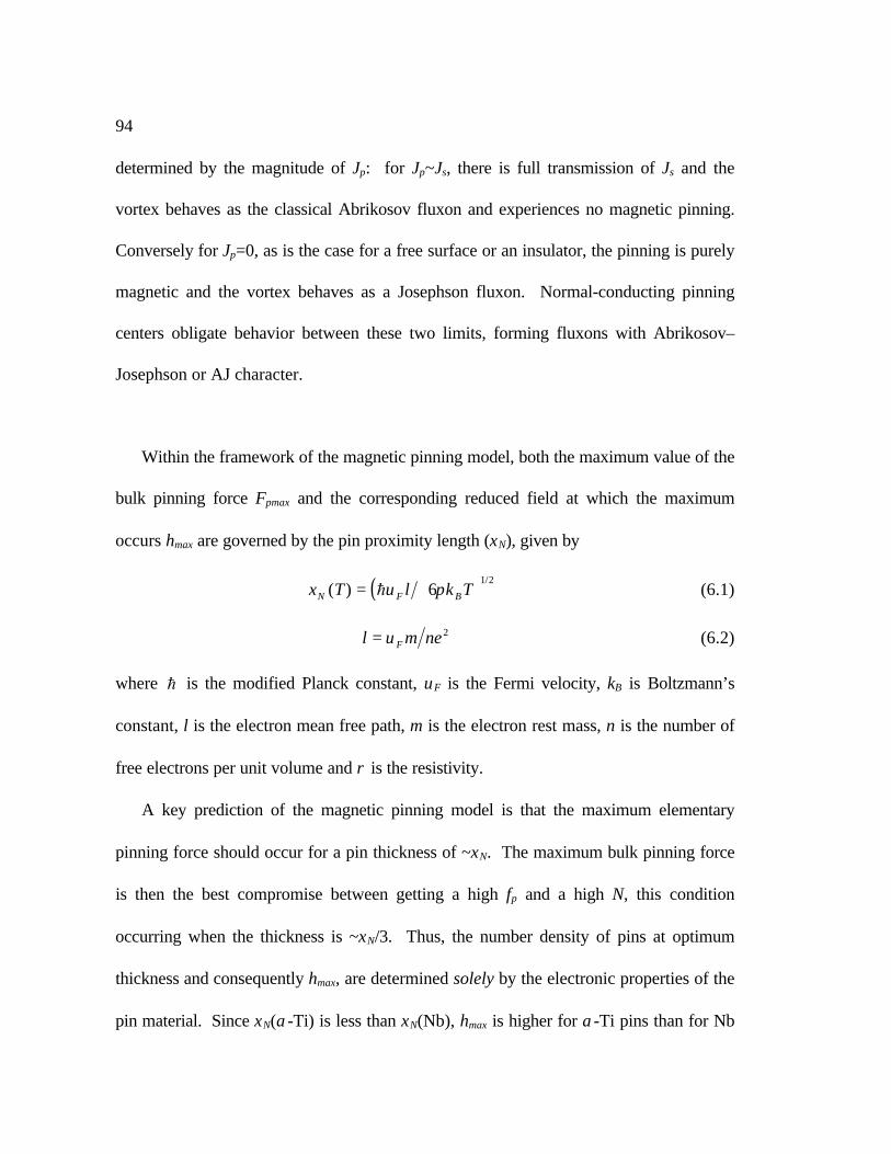
94
determined by the magnitude of Jp: for Jp~Js, there is full transmission of Js and the
vortex behaves as the classical Abrikosov fluxon and experiences no magnetic pinning.
Conversely for Jp=0, as is the case for a free surface or an insulator, the pinning is purely
magnetic and the vortex behaves as a Josephson fluxon. Normal-conducting pinning
centers obligate behavior between these two limits, forming fluxons with Abrikosov–
Josephson or AJ character.
Within the framework of the magnetic pinning model, both the maximum value of the
bulk pinning force Fpmax and the corresponding reduced field at which the maximum
occurs hmax are governed by the pin proximity length (ξN), given by
( )ξ υ πN F BT l k T( )/
= h 61 2
(6.1)
l m neF= υ 2 (6.2)
where h is the modified Planck constant, υF is the Fermi velocity, kB is Boltzmann’s
constant, l is the electron mean free path, m is the electron rest mass, n is the number of
free electrons per unit volume and ρ is the resistivity.
A key prediction of the magnetic pinning model is that the maximum elementary
pinning force should occur for a pin thickness of ~ξN. The maximum bulk pinning force
is then the best compromise between getting a high fp and a high N, this condition
occurring when the thickness is ~ξN/3. Thus, the number density of pins at optimum
thickness and consequently hmax, are determined solely by the electronic properties of the
pin material. Since ξN(α-Ti) is less than ξN(Nb), hmax is higher for α-Ti pins than for Nb

95
pins. The fact that this is observed experimentally suggests that alloyed Nb pins will
exhibit increased values of hmax.
In order to test these predictions, APC wires with alloyed Nb pins were fabricated,
the aims being (1) to reduce the pin proximity length by shortening the electron mean
free path and (2) to maintain a Nb-rich composition to allow for comparison with already
existing APC composites made with pure Nb pins. The second point is particularly
important when considering that pins with crystal structures other than the body centered
cubic (bcc) structure of Nb can produce markedly different nanostructures. Both Nb 7.5
wt.% Ta and Nb 10 wt.% W form bcc substitutional solid solutions, exhibit room
temperature strain hardening characteristics that are similar to Nb 47 wt.% Ti, and have
proximity lengths that are significantly shorter, 30% and 60% respectively, than that of
pure Nb. Hence, they make good candidates for artificial pins.
6.1 Experimental design
Pin proximity lengths were calculated using Equations 6.1 and 6.2 and the resistivities of
0.23 mm diameter wires measured at 10 K. The pin resistivities were measured in a
variable temperature cryostat using a 100 mA current and a 10 cm voltage tap spacing.
Although the values of ξN are higher than those established by Cooley et al. [52], no
attempt is made here to correct for the simple classical expressions of Equations 6.1 and
6.2.
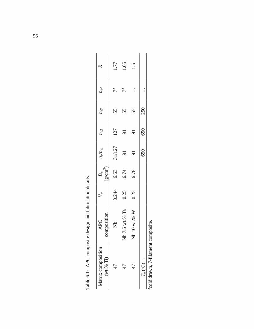
96
Tabl
e 6.
1: A
PC
com
posi
te d
esig
n an
d fa
bric
atio
n de
tail
s.
Mat
rix
com
posi
tion
(wt.%
Ti)
AP
Cco
mpo
siti
onV
pD
c
(g/c
m3 )
n p/n
e1n e
2n e
3n e
4R
47N
b0.
244
6.63
31/1
2712
755
7a1.
77
47N
b 7.
5 w
t.% T
a0.
256.
7491
9155
7a1.
65
47N
b 10
wt.%
W0.
256.
7891
9155
…1.
5
Te (
o C)
→65
065
025
0…
a cold
dra
wn,
7-f
ilam
ent c
ompo
site
.

97
Table 6.1 summarizes the fabrication details for the three APC composites. The Nb-
pin APC composite was fabricated using the rod-based APC process and contained 24.4
vol.% of pins [106]. A comprehensive analysis of its microstructure and Jc properties
was presented in chapter 4.
The alloyed Nb-pin APC composites were fabricated using the island-type method
first described in [27], in which a rod of the pin material is inserted into a hole drilled
into a rod of Nb-Ti. In this case the pin diameter was half that of the Nb-Ti rod, yielding
a pin volume fraction of 25%. Previous analysis of strain hardening in the Nb 10 wt.%
W [107] showed an increased strain hardening compared to that for single-phase Nb 47
wt.% Ti [108]. Therefore, in order to minimize differential hardening between the two
materials during reduction, the Nb 10 wt.% W rod was heat treated for 6 hr at 1300 oC
prior to billet assembly. This heat treatment was designed to recrystallize the Nb 10
wt.% W and develop a fine-grained equiaxed grain structure to minimize the type of bcc
plane-strain induced shape degradation discussed in chapter 3. In preparation for heat
treatment, the Nb 10 wt.% W rod was wrapped in Nb foil and inserted within a 14 mm
ID × 16 mm OD quartz tube, along with a Nb-foil-wrapped titanium getter. The quartz
tube was evacuated to <10–3 Pa for 12 hr and sealed off under 50 kPa of argon to
minimize the evaporation of Ti inside the vessel during heat treatment. After
encapsulation, the Ti getter was locally heated to red heat in order to absorb any
remaining residual gases. During heat treatment a cover gas of argon was flowed over
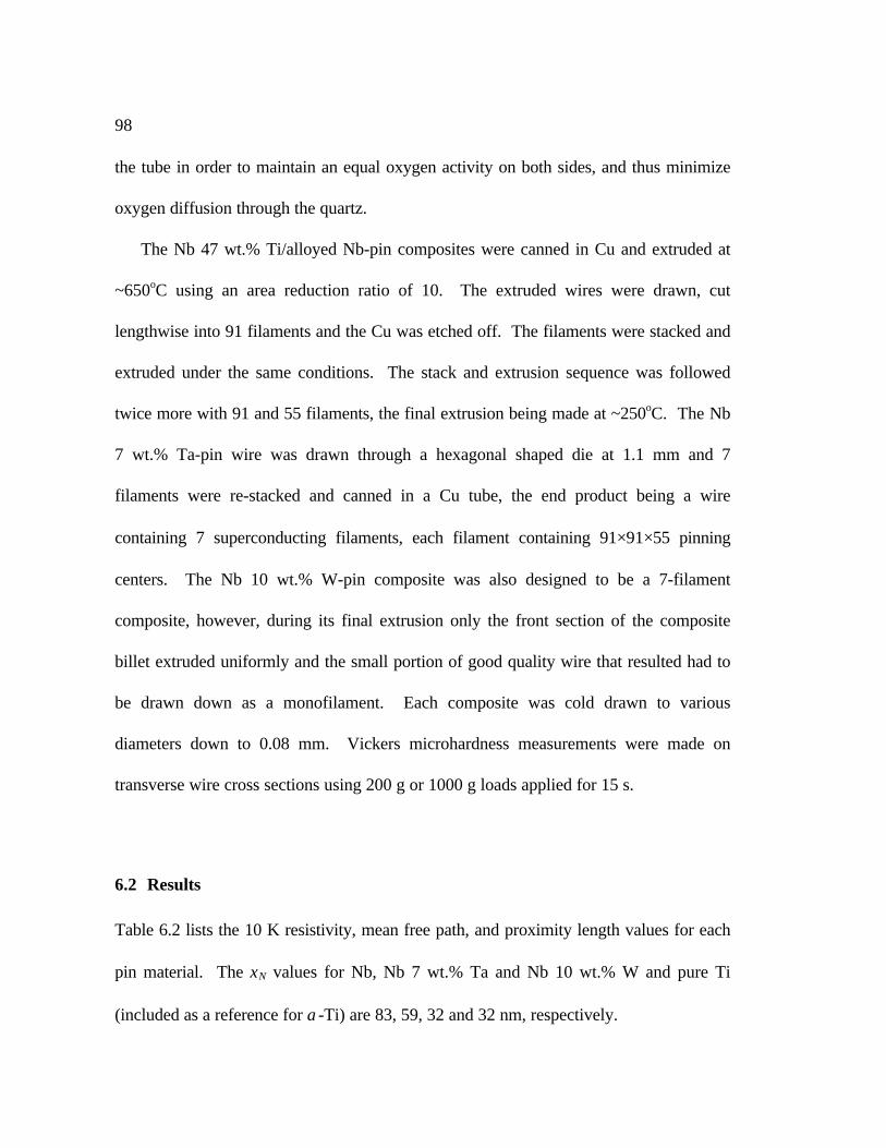
98
the tube in order to maintain an equal oxygen activity on both sides, and thus minimize
oxygen diffusion through the quartz.
The Nb 47 wt.% Ti/alloyed Nb-pin composites were canned in Cu and extruded at
~650oC using an area reduction ratio of 10. The extruded wires were drawn, cut
lengthwise into 91 filaments and the Cu was etched off. The filaments were stacked and
extruded under the same conditions. The stack and extrusion sequence was followed
twice more with 91 and 55 filaments, the final extrusion being made at ~250oC. The Nb
7 wt.% Ta-pin wire was drawn through a hexagonal shaped die at 1.1 mm and 7
filaments were re-stacked and canned in a Cu tube, the end product being a wire
containing 7 superconducting filaments, each filament containing 91×91×55 pinning
centers. The Nb 10 wt.% W-pin composite was also designed to be a 7-filament
composite, however, during its final extrusion only the front section of the composite
billet extruded uniformly and the small portion of good quality wire that resulted had to
be drawn down as a monofilament. Each composite was cold drawn to various
diameters down to 0.08 mm. Vickers microhardness measurements were made on
transverse wire cross sections using 200 g or 1000 g loads applied for 15 s.
6.2 Results
Table 6.2 lists the 10 K resistivity, mean free path, and proximity length values for each
pin material. The ξN values for Nb, Nb 7 wt.% Ta and Nb 10 wt.% W and pure Ti
(included as a reference for α-Ti) are 83, 59, 32 and 32 nm, respectively.
99
An analysis of the fractured Nb 10 wt.% W-pin composite following the final
extrusion is presented in Figure 6.1. Figure 6.1(a) shows a portion of the as-extruded
Nb 10 wt.% W pin wire. Circumferential striations are barely visible at 3 cm intervals
along the length of the wire. Figure 6.1(b) shows the same section of wire after the
copper sheath was etched away, revealing a highly fractured Nb-Ti/Nb-W core, the
fractures forming a succession of tear-drop shaped 1–2 cm long pieces. Figure 6.1(c)
shows a graph of extrusion pressure as a function of time recorded for this composite;
the periodic core fracture shown in Figure 6.1(b) manifested as periodic spikes in the
pressure. The circled portion of the pressure trace indicates a very short interval of
uniform deformation near the outset of the extrusion cycle, precisely the short section of
monofilamentary wire which was subsequently drawn to final size and characterized.
Figures 6.2(a)–(c) show FESEM secondary-electron micrographs of the Nb, Nb 7
wt.% Ta and Nb 10 wt.% W composites, respectively, at dp~400 nm. At this size, still
an factor of ~10 larger than optimum size, the pin shape is irregular but the designed
hexagonal pin arrangement is still apparent. The only noticeable difference between the
Table 6.2: Artificial pin electronic properties at 10 K.
Pin material Dp
(g/cm3)ρ0
(µΩ-cm)l
(nm)ξN
(nm)Nb 8.55 0.567 53 83
Nb 7.5 wt.% Ta 4.51 1.11 27 59Nb 10 wt.% W 9.01 3.67 7.7 32
Ti 8.80 5.61 6.1 32

100
(a)
(b)
(c)
x
300 MPa
1 cm
Figure 6.1: Analysis of the fractured Nb 10 wt.% W-pin composite following its finalextrusion. Figure 6.1(a) shows a portion of the composite after the final extrusion.Circumferential striations are barely visible at 3 cm intervals along the length of the wire.6.1(b) shows the same section of wire after the Cu sheath was etched away revealing thehighly fractured Nb-Ti/Nb-W core. 6.1(c) shows a graph of extrusion pressure as afunction of distance; the periodic fractures shown in (b) are manifested as spikes in thepressure. The vertical arrow in (c) indicates a very short interval of uniform deformationnear the outset of the extrusion cycle, precisely the section of wire which was drawn tofinal size.
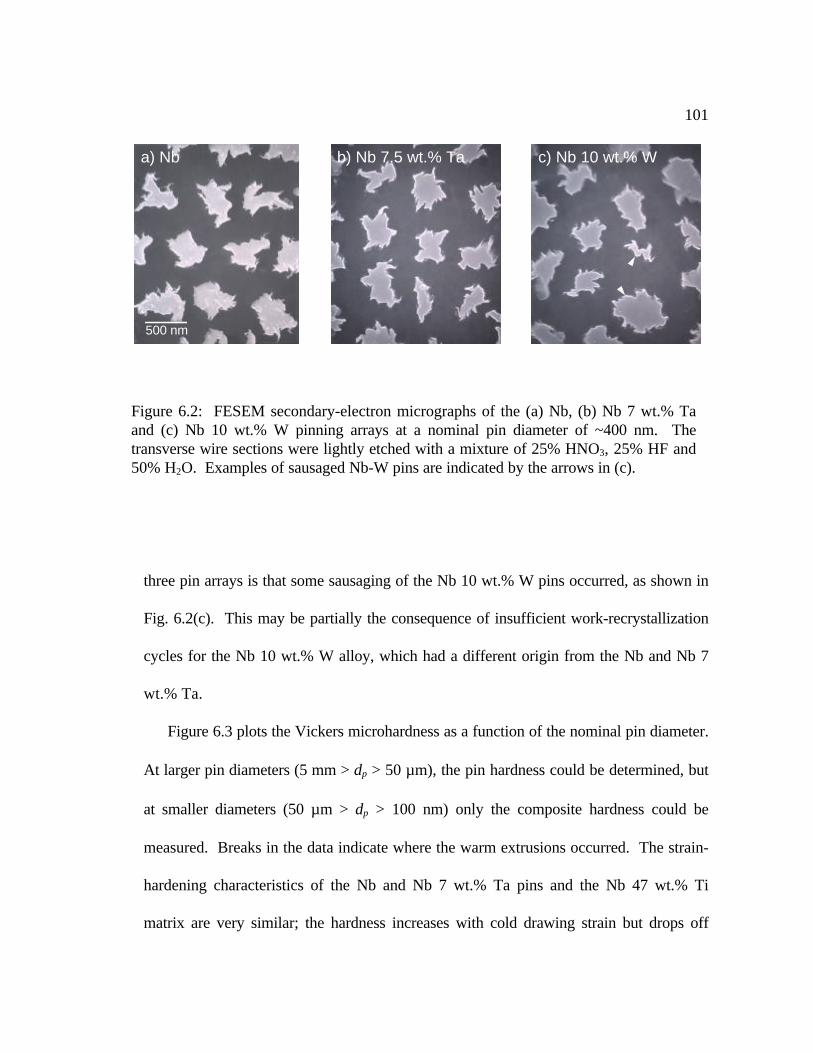
101
three pin arrays is that some sausaging of the Nb 10 wt.% W pins occurred, as shown in
Fig. 6.2(c). This may be partially the consequence of insufficient work-recrystallization
cycles for the Nb 10 wt.% W alloy, which had a different origin from the Nb and Nb 7
wt.% Ta.
Figure 6.3 plots the Vickers microhardness as a function of the nominal pin diameter.
At larger pin diameters (5 mm > dp > 50 µm), the pin hardness could be determined, but
at smaller diameters (50 µm > dp > 100 nm) only the composite hardness could be
measured. Breaks in the data indicate where the warm extrusions occurred. The strain-
hardening characteristics of the Nb and Nb 7 wt.% Ta pins and the Nb 47 wt.% Ti
matrix are very similar; the hardness increases with cold drawing strain but drops off
b) Nb 7.5 wt.% Ta c) Nb 10 wt.% Wa) Nb
500 nm
Figure 6.2: FESEM secondary-electron micrographs of the (a) Nb, (b) Nb 7 wt.% Taand (c) Nb 10 wt.% W pinning arrays at a nominal pin diameter of ~400 nm. Thetransverse wire sections were lightly etched with a mixture of 25% HNO3, 25% HF and50% H2O. Examples of sausaged Nb-W pins are indicated by the arrows in (c).
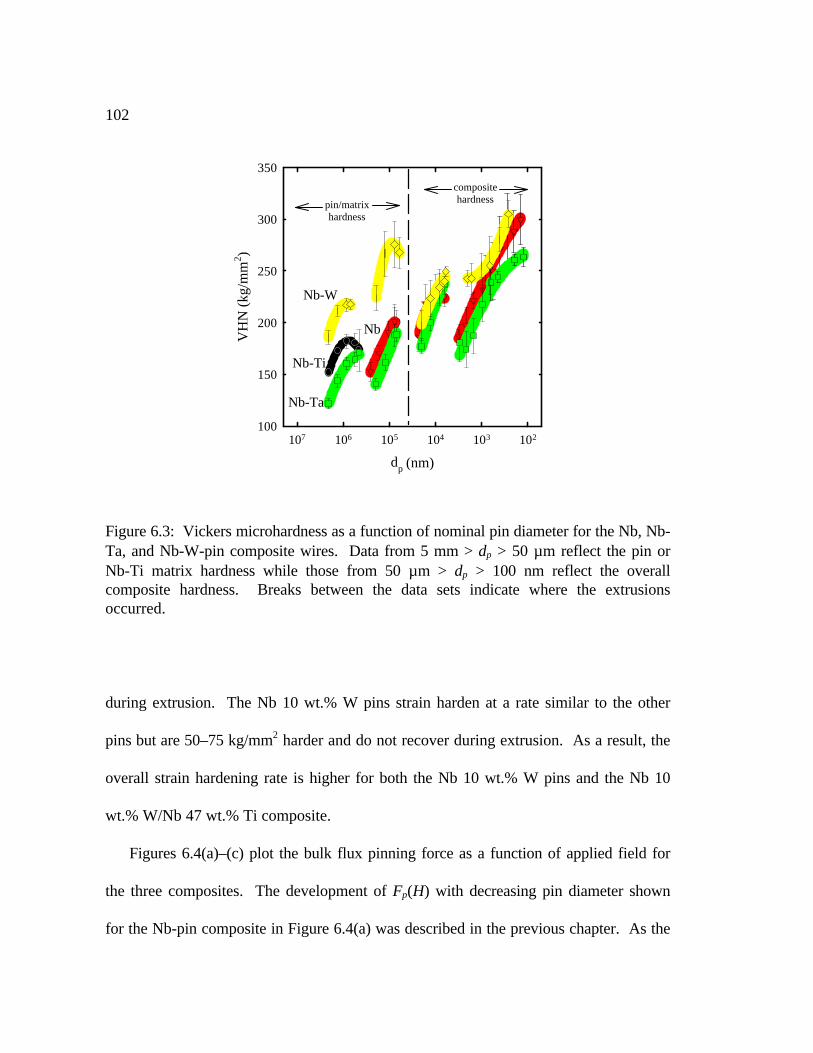
102
during extrusion. The Nb 10 wt.% W pins strain harden at a rate similar to the other
pins but are 50–75 kg/mm2 harder and do not recover during extrusion. As a result, the
overall strain hardening rate is higher for both the Nb 10 wt.% W pins and the Nb 10
wt.% W/Nb 47 wt.% Ti composite.
Figures 6.4(a)–(c) plot the bulk flux pinning force as a function of applied field for
the three composites. The development of Fp(H) with decreasing pin diameter shown
for the Nb-pin composite in Figure 6.4(a) was described in the previous chapter. As the
dp (nm)
102103104105106107
VH
N (
kg/m
m2 )
100
150
200
250
300
350
pin/matrixhardness
compositehardness
Nb
Nb-Ti
Nb-Ta
Nb-W
Figure 6.3: Vickers microhardness as a function of nominal pin diameter for the Nb, Nb-Ta, and Nb-W-pin composite wires. Data from 5 mm > dp > 50 µm reflect the pin orNb-Ti matrix hardness while those from 50 µm > dp > 100 nm reflect the overallcomposite hardness. Breaks between the data sets indicate where the extrusionsoccurred.
103
nominal pin diameter decreased below 100 nm, a low field peak in Fp(H) emerged,
reaching a maximum value of 32 GN/m3 at 2.5 T for dp~40 nm. When the pin size was
further reduced, the peak position shifted to higher fields, but the magnitude declined. A
similar development of Fp(H) with decreasing pin diameter is shown for the Nb 7 wt.%
Ta-pin composite in Figure 6.4(b). In this case Fpmax reached 25 GN/m3, but at higher
field (3 T) and smaller dp (35 nm). It should be noted that low field flux jumps in the
wires with dp>35 nm may have prevented measurement of the true Fpmax.
The development of Fp(H) over the interval dp=82–32 nm in the Nb 10 wt.% W-pin
composite shown in Figure 6.4(c), differs qualitatively from that observed for the pure
Nb and Nb 7 wt.% Ta-pin composites. It bears a closer resemblance to the development
of Fp(H) seen in conventionally processed Nb 47 wt.% Ti during the drawing strain at
large pin size following the last precipitation heat treatment (see Figure 1.8). As in the
other APC composites, a low field peak in Fp(H) develops at large dp, but the optimum
curve is not reached, at least until dp=32 nm (the smallest wire tested). The peak value
of Fp, 15 GN/m3, appears to still be rising with decreasing dp because there is a
comparatively larger increase of Fp with changing dp at this size than is seen in Figures
6.4(a) and (b) near the optimum value of dp.
6.3 Discussion
As expected, the proximity length of the Nb pins decreased with alloying. The proximity
lengths of Nb 7 wt.% Ta (59 nm) and Nb 10 wt.% W (32 nm) are 30% and
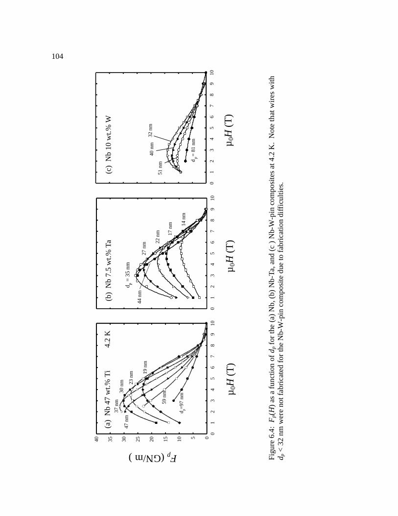
104
01
23
45
67
89
100510152025303540
(a)
Nb
47 w
t.% T
i
d p=97
nm
59 n
m
47 n
m
37 n
m30
nm 23
nm 19
nm
4.2
K
01
23
45
67
89
10
(b)
Nb
7.5
wt.%
Ta
d p =
35
nm
14 n
m
17 n
m
22 n
m
27 n
m44
nm
01
23
45
67
89
10
(c)
Nb
10 w
t.% W
dp =
81
nm
32 n
m40
nm
51 n
m
Figu
re 6
.4:
Fp(
H)
as a
fun
ctio
n of
dp
for
the
(a)
Nb,
(b)
Nb-
Ta, a
nd (
c )
Nb-
W-p
in c
ompo
site
s at
4.2
K.
Not
e th
at w
ires
with
d p <
32
nm w
ere
not f
abri
cate
d fo
r th
e N
b-W
-pin
com
posi
te d
ue to
fab
rica
tion
diff
icul
ties.
Fp (GN/m)
µ 0H
(T
)µ 0
H (
T)
µ 0H
(T
)
105
60% shorter, respectively, than that of pure Nb (83 nm). Nb 10 wt.% W has the same
proximity length as found for pure Ti, but ξN for α-Ti is likely even shorter because it is
alloyed with ~5 at.% Nb [21].
The trends seen in the Fp(H, dp) curves of Figure 6.4 are qualitatively consistent with
the magnetic pinning model. As the pin proximity length was reduced, the value of hmax
increased and Fpmax occurred at smaller nominal pin diameters. Stronger validation of the
magnetic pinning model may come with the identification of hmax and Fpmax in the Nb 10
wt.% W-pin composite, which unfortunately, was not possible in this study due to the
fabrication difficulties discussed above.
APC fabrication improvements are still being made. Our earlier work on pure Nb-
pin APC composites (chapter 4) produced large increases (~40%) in Fpmax with little
change in hmax. Nb 7.5 wt.% Ta is almost identical to Nb in hardness, work-hardening
and fabricability. However, the Nb 10 wt.% W was markedly worse, undoubtedly
because W has a smaller atomic radius (0.142 nm) than both Nb and Ta (0.147 nm),
causing the increased work-hardening behavior shown in Figure 6.3. However, the 32
nm limit placed on the Nb 10 wt.% W pin diameter in this experiment should not be
considered as a severe obstacle to fabricating wires with smaller nominal pin size.
Composite fracture during the final extrusion may have been more a result of the billet
design and extrusion parameters not being optimized for the higher overall Nb 47 wt.%
Ti/Nb 10 wt.% W composite hardness, rather than as a direct consequence of the
pin/matrix hardness disparity. This hypothesis is supported by the fact that the Nb 10
106
wt.% W-pin wire drew well following the final extrusion; the pin sausaging observed in
Figure 6.2(c) did not adversely affect its ductility. Thus a key to improving composite
fabricability in this particular case may lie in simple adjustments of one or more of the
extrusion parameters. Predictive equations by Avitzur [59] suggest that making the Nb-
Ti/Nb-W and matrix more similar by increasing the matrix flow stress (e.g. using Cu 30
wt.% Ni instead of Cu) or decreasing the copper-to-superconductor ratio are two means
for promoting uniform composite deformation during extrusion. These modifications are
easily implemented and indeed desirable because neither requires an increase in the
extrusion temperature. New composites utilizing these design modifications are
currently in manufacture.
6.4 Conclusions
Nb 47 wt.% Ti wires containing 25 vol.% of alloyed Nb pins were fabricated to evaluate
the effect of the pin proximity length ξN on the flux pinning properties. The proximity
length of pure Nb, 83 nm, decreased to 59 nm and 32 nm when alloyed with 7.5 wt.% Ta
and 10 wt.% W, respectively. The field and pin thickness dependence of Fp qualitatively
support the magnetic pinning model; as ξN decreased, the field and pin thickness at which
the maximum Fp occurred increased and decreased, respectively. Excessive hardening of
the Nb 10 wt.% W-pin composite, an adverse effect of the tungsten alloying addition,
caused non-uniform composite deformation during the final extrusion and prevented
wires with dp<32 nm from being fabricated.
107
7. Summary
Superconducting Nb-Ti wires containing uniform arrays of Nb artificial pinning centers
were fabricated and their microstructures and electromagnetic properties characterized
as the pin size and spacing were reduced to the nanometer dimensions of the flux line
lattice. Through careful control of the thermomechanical treatment, the critical current
density of a composite containing Nb 47 wt.% Ti with 24 volume percent of Nb pins was
raised to 4600 A/mm2 at the benchmark field (5 T) and temperature (4.2 K), thus
establishing a new record for any round-wire of Nb-Ti. Maximum Jc(5 T) occurred for a
nominal pin diameter (dp) of 25 nm, but for which the actual pins were 1–15 nm thick
elongated ribbons.
However, the high-field (>6 T) flux pinning in this Nb-pin wire was significantly
lower than is achieved in conventional processed Nb-Ti, mainly because (1) Hc2 and H*
108
were depressed by ~1.5 T as compared to optimized, conventional Nb-Ti, and (2) Fp(H)
peaked at ~0.3Hc2 rather than at 0.5Hc2 as is found for conventional Nb-Ti.
Two separate attempts were made to improve the high-field flux pinning of Nb-pin
APC wires. The first attempt involved increasing the titanium content of the Nb-Ti
matrix in order to raise both Hc2 and H* in the proximity-effect coupled limit (i.e. when
the pin thickness is less than ξ). A Nb 62 wt.% Ti-matrix composite, designed for
maximum upper critical field in the coupled limit, exhibited an increased H* as the pin
size was reduced. However, the enhancement was significantly less than predicted in the
fully coupled limit, even when the pin thickness was much smaller than ξ. In the context
of existing proximity effect models, this can be attributed to the same minimal pin/matrix
interdiffusion held responsible for high Jc in the low to mid field range of 1–5 T.
A second attempt to improve the high field pinning involved decreasing the pin
proximity length (ξN) in order to shift the maximum in the bulk pinning force curve to
higher field, in accordance with the magnetic pinning model of Cooley, Lee, and
Larbalestier [52]. Through separate alloying additions of 7.5 wt.% Ta and 10 wt.% W
the Nb-pin proximity length was reduced by 30% and 60%, respectively. The functional
dependence of the bulk flux pinning force on ξN, dp, and H agreed qualitatively with the
magnetic pinning model. However, excessive hardening of the Nb-W-pin composite, an
adverse effect of the tungsten alloying addition, caused non-uniform composite
deformation during the final extrusion and prevented the full effect on Fp(H, dp) from
being evaluated.
109
Finally, during the course of this thesis, a robust process for fabricating APC wires
with large filament diameters and uniform pin arrays was developed. This process
should be readily applicable to a wide variety of artificial pin materials. However, as
illustrated by the Nb 10 wt.% W-pin composite, processing modifications will
continually need to be made to accommodate pins with mechanical properties which
differ significantly from those of the Nb-Ti matrix.

110
111
Bibliography
[1] F. London and H. London, Proc. Roy. Soc. (London) A155, 71 (1935).
[2] A.B. Pippard, Physica 19, 765 (1953).
[3] V. Ginzburg and L. Landau, Zh. Eksperim. I Thor. Fiz. 20, 1064 (1950).
[4] A.C. Rose-Innes and E.H. Rhoderick, Introduction to Superconductivity,Pergamon Press, Oxford (1978).
[5] W. Meissner and R. Ochsenfeld, Naturwissen 21, 787 (1933).
[6] A.A. Abrikosov, Soviet Physics JETP 5, 1174 (1957).
[7] A.M. Campbell and J.E. Evetts, Adv. Phys. 21, 199 (1972).
[8] E.J. Kramer and H.C. Freyhardt, J.Appl. Phys. 51, 4930 (1980).
[9] T. Matsushita, J. Appl. Phys. 54, 281 (1983).
[10] C. Meingast and D.C. Larbalestier, J. Appl. Phys. 66, 5962 (1989).
[11] G. Stejic, Ph.D. Thesis, University of Wisconsin–Madison (1993).

112
[12] H. Ullmaier, Irreversible Properties of Type-II Superconductors, Springer-Verlag, Berlin (1975).
[13] X.G. Qiu, S. Takahashi and M. Tachiki, Physica C 216, 49 (1993).
[14] W.E. Yetter, D.A. Thomas, and E.J. Kramer, Phil. Mag. B 46, 523 (1982).
[15] W. Fietz and W. Webb, Phys. Rev. 178, 657 (1969).
[16] D. Dew-Hughes, Phil. Mag. 55, 459 (1987).
[17] D.C. Larbalestier and A.W. West, Acta Met. 32, 1871 (1984).
[18] D.C. Larbalestier, A.W. West, W.L. Starch, W. Warnes, P.J. Lee, W.K.McDonald, P. O’Larey, K. Hemachalem, B. Zeitlin, R. Scanlan and C. Taylor,IEEE Trans. MAG. 21, 269 (1985).
[19] M.J. Buckett and D.C. Larbalestier, IEEE Trans. MAG. 23, (1987).
[20] Li Chengren and D.C. Larbalestier, Cryogenics 27, 171 (1987).
[21] P.J. Lee and D.C. Larbalestier, Acta Met. 35, 2523 (1987).
[22] P.J. Lee and D.C. Larbalestier, J. Mat. Sci. 23, 3951 (1988).
[23] C. Meingast, P.J. Lee and D.C. Larbalestier, J. Appl. Phys 66, 5962 (1989).
[24] P.J. Lee, J.C. McKinnell, and D.C. Larbalestier, Adv. Cryo. Engr. 36A, 287(1990).
[25] G. Stejic, L.D. Cooley, R. Joynt, and D.C. Larbalestier, Supercond. Sci. Tech. 5,S176 (1992).
[26] G.L. Dorofejev, E.Y. Klimenko, S.V. Frolov, E.V. Nikulenkov, E.I. Plashkin,N.I Salunin, and V.Y. Filkin, Proceedings of the Ninth International Conferenceon Magnet Technology, Ed. By C. Marinucci and P. Weymuth (pub. SwissInstitute for Nuclear Research, Villigen, Switzerland) 564 (1985).
[27] B.A. Zeitlin, M.S. Walker, and L.R. Motowidlo, United States Patent No.4,803,310 (Jan. 7, 1989).
113
[28] L.R. Motowidlo, H.C. Kanithi, and B.A. Zeitlin, Adv. Cryo. Eng. 36A, 311(1990).
[29] L.D. Cooley, Ph.D. Thesis, University of Wisconsin–Madison (1992).
[30] L.D. Cooley, P.J. Lee, D.C. Larbalestier, and P.M. O’Larey, Appl. Phys. Lett.64, 1298 (1994).
[31] K. Matsumoto, Y.Tanaka, K. Yamafuji, K. Funaki, M. Iwakuma, and T.Matsushita, IEEE Trans Appl. Supercond. 3, 1362 (1993).
[32] K. Matsumoto, Y. Tanaka, K. Yamada, O. Miura, United States Patent No.5,374,320 (Dec. 20, 1994).
[33] K. Matsumoto, H. Takewaki, Y. Tanaka, O. Miura, K. Yamafuji, K. Funaki, M.Iwakuma, and T. Matsushita, Appl. Phys. Lett. 64, 115 (1994).
[34] J. Wong, M.K. Rudziak, D. W. Capone II, United States Patent No. 5,158,620(Oct. 27, 1992); J. Wong, M.K. Rudziak, United States Patent No. 5,160,550(Nov. 3, 1992); J. Wong, M.K. Rudziak, D. W. Capone II United States PatentNo. 5,160,794 (Nov. 3, 1992); J. Wong, M.K. Rudziak, United States Patent No.5,223,348 (June 29, 1993).
[35] T. Wong, M. K. Rudziak, J.M. Seuntjens, and J. Wong, IEEE Trans. Appl.Supercond. 7, 1126 (1996).
[36] R.W. Heussner, P.D. Jablonski, and D.C. Larbalestier, proceedings of the LowTemperature Superconductor Workshop, Devil’s Head, WI, Feb. 8–10 (1994).
[37] N.D. Rizzo, S. Ling, J.D. McCambridge, D. Prober, L. R. Motowidlo and B.A.Zeitlin, proceedings of the Low Temperature Superconductor Workshop, Devil’s
[38] P.D. Jablonski and D.C. Larbalestier, United States Patent No. 5,226,947 (July13, 1993).
[39] P.D. Jablonski, Ph.D. Thesis, University of Wisconsin–Madison (1994).
[40] P.D. Jablonski, P.J. Lee, and D.C. Larbalestier, Mat.Res. Soc. Symp. Proc. 351,455 (1994).
114
[41] P.D. Jablonski, P.J. Lee, and D.C. Larbalestier, Appl. Phys. Lett. 65, 767 (1994).
[42] L.N. Cooper, Phys. Rev. Letters 6, 89 (1961).
[43] P.G. de Gennes, Rev. Mod. Phys. 36, 255 (1964).
[44] P.G. de Gennes, Superconductivity of Metals and Alloys, W.A. Benjamin, NewYork (1966).
[45] N.R. Werthamer, Phys. Rev. 132, 2440 (1963).
[46] W. Silvert, J. Low Temp. Phys. 20, 439 (1975).
[47] H. Muller (unpublished).
[48] L.R. Motowidlo, B.A. Zeitlin, M.S. Walker, and P Haldar, Appl. Phys Lett. 61991 (1992)
[49] L.D. Cooley (unpublished).
[50] L.D. Cooley, P.J. Lee, and D.C. Larbalestier, IEEE Trans. Mag. 27, 1097(1991).
[51] A. Gurevich and L.D. Cooley, Phys. Rev. B 50, 13563 (1994).
[52] L.D. Cooley, P.J. Lee, and D.C. Larbalestier, Phys. Rev. B 53, 6638 (1996).
[53] L.D. Cooley, to appear Adv. Cryo. Eng. 42, (1998).
[54] R.W. Heussner, C.B. Nunes, P.D. Jablonski, P.J. Lee, and D.C. Larbalestier, J.Appl. Phys. 80, 1640 (1996).
[55] P.J. Lee, D.C. Larbalestier, and P.D. Jablonski, IEEE Trans. Appl. Supercond. 5,1701 (1995).
[56] M.N. Wilson, Superconducting Magnets, Oxford Press, New York (1983).
[57] N.D. Rizzo, Ph.D. Thesis, Yale University (1997).
[58] B. Avitzur, Trans. ASME Eng. for Ind. 90, 79 (1968).

115
[59] B. Avitzur, Handbook of Metal-Forming Processes, John Wiley & Sons (1983).
[60] B. Avitzur R. Wu, S. Talbert, and Y.T. Chou, Trans. ASME Eng. for Ind. 108,133 (1986).
[61] B. Avitzur and W. Pachla, Trans. ASME Eng. for Ind. 108, 295 (1986).
[62] B. Avitzur and W. Pachla, Trans. ASME Eng. for Ind. 108, 307 (1986).
[63] E.W. Collings, Applied Superconductivity, Metallurgy and Physics of TitaniumAlloys, Plenum Press, New York (1986).
[64] T.H. Courtney, Mechanical Behavior of Materials, McGraw-Hill PublishingCompany, New York (1990).
[65] D.C. Larbalestier, P.J. Lee, and R.W. Samuel, Adv. Cryo. Eng. 32, 715 (1986).
[66] K. J. Faase, P.J. Lee, and D.C. Larbalestier, Adv. Cryo. Eng. 38, 723 (1992).
[67] W.H. Warnes and D.C. Larbalestier, Cryogenics 26, 643 (1986).
[68] W.H. Warnes, J. Appl. Phys. 63, 1651 (1988).
[69] Y.E. High, J.C. McKinnell, P.J. Lee and D.C. Larbalestier, Adv. Cryo. Eng. 38,647 (1992).
[70] L. Kaufman and H. Bernstein, Computer Calculations of Phase Diagrams,Academic Press, New York (1970).
[71] D.L. Moffat, Ph.D. Thesis, University of Wisconsin–Madison (1986).
[72] A. Parekh, Undergraduate Senior Thesis, University of Wisconsin–Madison(1988).
[73] Hydrostatic extrusion press manufactured by Naples Research andManufacturing, Inc., Naples, FL.
[74] F. J. Fuchs, United States Patent No. 4,751,058 (June 14, 1988).
[75] E. Gregory, T.S. Kreilick, J. Wong, A.K. Gosh, and W.B. Sampson, Cryogenics27, 178 (1987).

116
[76] Z. Guo, Ph.D. Thesis, Oregon State University (1994).
[77] J.C. McKinnell, Ph.D. Thesis, University of Wisconsin–Madison (1990).
[78] C.P. Bean, Rev. Mod. Phys. 36, 31 (1964).
[79] P.D. Jablonski (unpublished).
[80] C.B. Nunes, R.W. Heussner, and D.C. Larbalestier, J. Appl. Phys. 80, 1647(1996).
[81] C.B. Nunes, R.W. Heussner, and D.C. Larbalestier, IEEE Trans. Appl.Supercond. 7, 1138 (1997).
[82] M. Suenaga, A.K. Ghosh, Y. Xu, and D.O. Welch, Phys. Rev. Lett. 66, 1777(1991).
[83] L.A. Bonney, T.C. Willis, and D.C. Larbalestier, J. Appl. Phys. 77, 6377 (1995).
[84] These data come from a 61-filament multifilamentary Nb 47 wt.% Ti compositefabricated at the University of Wisconsin–Madison Applied SuperconductivityCenter and designated CB9738. The composite processing included 3 × 80hr/420 oC heat treatments. It is among the highest Jc multifilamentary Nb-Ticomposites ever produced.
[85] J.F. Peck and D.A. Thomas, Trans. Met. Soc. AIME 221, 1240 (1961).
[86] W.F. Hosford, Trans. Met. Soc. AIME 230, 12 (1964).
[87] J.C. Malzahn Kampe and T.H. Courtney, Scripta MET. 23, 141 (1989).
[88] R.W. Heussner, P.J. Lee, and D.C. Larbalestier, IEEE Trans. Appl. Supercond.3, 757 (1993).
[89] R.W. Heussner, P.D. Jablonski, P.J. Lee, and D.C. Larbalestier, Adv. Cryo Eng.40, 755 (1994).
[90] C.B. Nunes (unpublished).

117
[91] L.R. Motowidlo, B.A. Zeitlin, M.S. Walker, P. Haldar, J.D. McCambridge, N.D.Rizzo, X.S. Ling, and D. E. Prober, IEEE Trans. Appl. Supercond. 3, 1366(1993).
[92] H.C. Kanithi, P. Valaris, L.R. Motowidlo, B.A. Zeitlin, and R.M. Scanlan, Adv.Cryo. Eng. 38, 675 (1992).
[93] R.W. Heussner, C.B. Nunes, L.D. Cooley, and D.C. Larbalestier, IEEE Trans.Appl. Supercond. 7, 1142 (1997).
[94] O. Miura, K. Matsumoto, Y. Tanaka, K. Yamafuji, N. Harada, M Iwakuma, K.Funaki, and T. Matsushita, Cryogenics 32, 315 (1992).
[95] K. Matsumoto, Y. Tanaka, K. Yamafuji, K, Funaki, M. Iwakuma, and T.Matsushita, Supercond. Sci. Tech. 5, 684 (1992).
[96] D.C. Larbalestier and A. West, Acta Met. 32, 1871 (1984).
[97] J.D. McCambridge, N.D. Rizzo, X.S. Ling, J.Q. Wang, D.E. Prober, L.R.Motowidlo, and B.A Zeitlin, IEEE Trans. Appl. Supercond. 5, 1697 (1995).
[98] E. Kadyrov, A. Gurevich, and D.C. Larbalestier, Appl. Phys. Lett. 68, 1567(1996).
[99] T. Matsushita and H. Küpfer, J. Appl. Phys. 63, 5048 (1988).
[100] M.T. Naus, R.W. Heussner, and D.C. Larbalestier, presented at the InternationalCryogenic Materials Conference, Portland, OR (1997).
[101] N. Sato, J. Appl. Phys. 67, 7493 (1990).
[102] Y.J. Qian, J.Q. Zheng, B.K. Sarma, H.Q. Yang, J.B. Ketterson, and J.E. Hilliard,J. Low Temp. Phys. 49, 279 (1982).
[103] W.H. Warnes, K.J. Faase, and J.A. Norris, to appear Adv. Cryo. Eng. 42,(1998).
[104] K.J. Faase, Ph.D. Thesis, Oregon State University (1996).
[105] M. Ledvij, L. Dobrosavljevic-Grujic, and J.R. Clem, Phys. Rev. B 38, 129(1988).
118
[106] R.W. Heussner, P.D. Jablonski, P.J. Lee, and D.C. Larbalestier, IEEE Trans.Appl. Supercond. 5, 1705 (1995).
[107] D. Ohmann (unpublished).
[108] J.A. Parrell, P.J. Lee, and D.C. Larbalestier, IEEE Trans. Appl. Supercond. 3,734 (1993).