Embed Size (px)
Citation preview

1
Flip-Chip for MM-Wave and Broadband Packaging
Wolfgang Heinrich
Ferdinand-Braun-Institut für Höchstfrequenztechnik (FBH)Berlin / Germany
with contributions by F. J. Schmückle
Motivation
Growing markets for mm-wave systems, e.g.
� 77 GHz automotive radar
� 60 GHz wireless communications
� 40 GHz radio links
� high bit-rate electronics(40 Gbps and beyond)
ICs are available: GaAs, SiGe, (CMOS)
What about packaging (low cost !)

2
Packaging a mm-wave IC (I)
As conventional - same as for VLSI chips ?
High frequency -> increased parasitics at interconnects
Packaging a mm-wave IC (II)
As conventional - same as for VLSI chips ?
High frequency -> increased parasitics at interconnects
General rule: keep dimensions small / electrically short
� compact mounting approach
� miniaturized interconnects
3
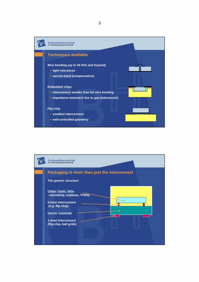
Techniques available
Wire bonding (up to 40 GHz and beyond)
� tight tolerances
� narrow-band (compensation)
Embedded chips
� interconnect smaller than for wire bonding
� impedance mismatch due to gap (tolerances!)
Flip-chip
� smallest interconnect
� well-controlled geometry
Packaging is more than just the interconnect
The generic structure
Chips: GaAs, SiGe- microstrip, coplanar, TFMSL
0-level interconnect(e.g. flip-chip)
Carrier substrate
1-level interconnect (flip-chip, ball grids)

4
Example: SMD chips at mm waves
United monolithic Semiconductors (UMS)
� Very attractive, but general approachfor mm-waves ?
This talk
Flip-chip for mm-wave and broadband packaging
� identify key issues from electrical / em design point of view
� provide understanding of mechanisms
Needs comprehensive view
� flip-chip interconnect
� carrier substrate & housing

5
Contents
The flip-chip interconnect
� overview on processes
� mm-wave & broad-band characteristics
� parasitic moding
� hot-via interconnect
The package
� thin-film & flip chip
� LTCC as carrier substrate
Conclusions
Flip-chip processes for mm-waves
Chip interconnect by means of bumps
Two technologies:
(i) Thermocompression
� Au bumps (using electroplating or stud bumps)
� bonding by thermocompression
(ii) Soldering
� e.g., AuSn bumps
� chip bonding & soldering in reflow oven
6
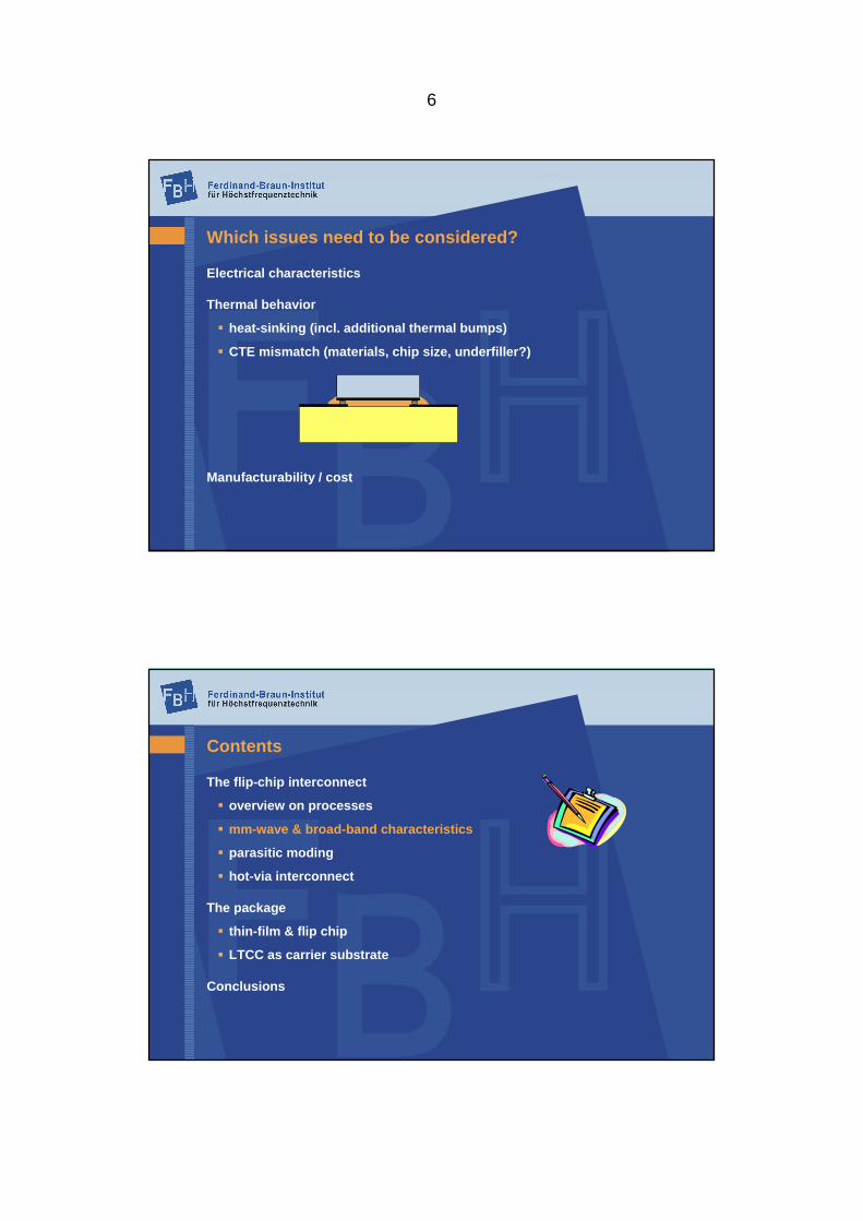
Which issues need to be considered?
Electrical characteristics
Thermal behavior
� heat-sinking (incl. additional thermal bumps)
� CTE mismatch (materials, chip size, underfiller?)
Manufacturability / cost
Contents
The flip-chip interconnect
� overview on processes
� mm-wave & broad-band characteristics
� parasitic moding
� hot-via interconnect
The package
� thin-film & flip chip
� LTCC as carrier substrate
Conclusions

7
A remark on 3D electromagnetic simulation
Tools used
� Based on finite-difference / finite-integration method
� F3D: FBH in-house code- frequency domain (FDFD)
� Microwave Studio (CST) - time domain (FDTD)
The flip-chip interconnect: mm-wave characteristics
Flip-chip approach
� well-known for lower frequencies
� suitable also for mm-wavesbecause of small dimensions
Two main RF effects
� detuning of on-chip circuit
� reflections at bump transition

8
Detuning
Changes of circuit behavior due to flip-chip mounting
Most critical elements: passives
� transmission lines
� spiral inductors
Underfiller has a particular influence
Transmission lines can be used as a benchmark
motherboard
chip
motherboard
chip
CPW : deviation β/ β0 and Z vs. bump height h
Chip: 50 µm wide CPW
With/without metalization on motherboard below chip
f = 50 GHz
10 20 30 40 50 60 70 80 90 100
bump height h [µm]
0
5
10
15
-5
-10
-15
devi
atio
n [%
]
beta (metal.) |Z| (metal.) beta |Z|
with metalization below chip
without metalization below chip
motherboard
chip
9
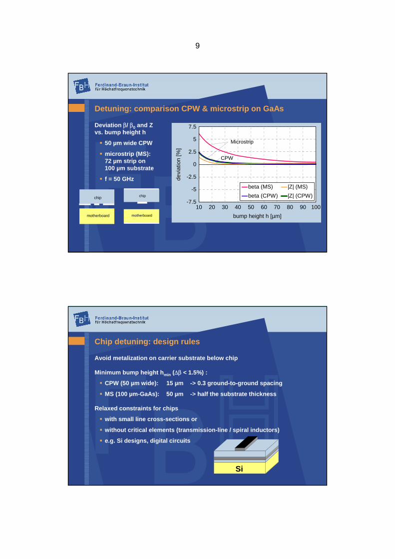
Detuning: comparison CPW & microstrip on GaAs
Deviation β/ β0 and Z vs. bump height h
� 50 µm wide CPW
� microstrip (MS): 72 µm strip on100 µm substrate
� f = 50 GHz
10 20 30 40 50 60 70 80 90 100
bump height h [µm]
0
2.5
5
7.5
-2.5
-5
-7.5
devi
atio
n [%
]
beta (MS) |Z| (MS)
beta (CPW) |Z| (CPW)
Microstrip
CPW
motherboard
chip
motherboard
chip
Chip detuning: design rules
Avoid metalization on carrier substrate below chip
Minimum bump height hmin (Δβ < 1.5%) :
� CPW (50 µm wide): 15 µm -> 0.3 ground-to-ground spacing
� MS (100 µm-GaAs): 50 µm -> half the substrate thickness
Relaxed constraints for chips
� with small line cross-sections or
� without critical elements (transmission-line / spiral inductors)
� e.g. Si designs, digital circuits
Si

10
Reflections at the interconnect
Basic structure: CPW-to-CPW transition
Bump geometry
� height h
� diameter land related quantities
- pad size lp- total width of transition
S11 for 80 µm bumps: Influence of bump height
3D FDFD simulations
Bump geometry
� diameter l = 80 µm
� pad size lp = 100 µm
� height h = 20…100 µm
|S11| for CPW mode vs. frequency
0 20 40 60 80 100
-25
-20
-15
-10
-5
bump height
100um 50um 20um
|S11
| (dB
)
Frequency (GHz)S11
motherboard
chip
CPW 1
chip
CPW 1
11
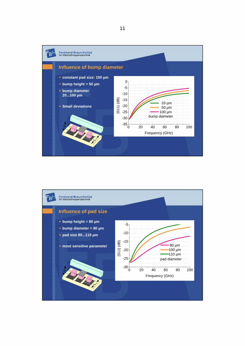
Influence of bump diameter
� constant pad size: 100 µm
� bump height = 50 µm
� bump diameter 20...100 µm
� Small deviations
0 20 40 60 80 100-35
-30
-25
-20
-15
-10
-5
0
bump diameter
20 µm 50 µm 100 µm|S
11| (
dB)
Frequency (GHz)
Influence of pad size
� bump height = 80 µm
� bump diameter = 80 µm
� pad size 80...110 µm
� most sensitive parameter
0 20 40 60 80 100-30
-25
-20
-15
-10
-5
pad diameter
80 µm100 µm110 µm|S
11| (
dB)
Frequency (GHz)

12
Comparison small / large bumps
0 20 40 60 80 100
-35
-30
-25
-20
-15
-10
-5
pad diameter 50 µmbump diameter 30 µmbump height 20 µm
pad diameter 100 µmbump diameter 80 µmbump height 80 µm
|S11
| (dB
)
Frequency (GHz)
� High-freqency performance depends on interconnect size
� 30 µm bumps: excellent broadband characteristics over 100 GHz
� In practice: 2 parameters dictate overall dimensions
- bump size- min. pad size &
spacing on carrier substrate
Electrical characteristics: capacitive or inductive ?
Two effects
� inductive (bumps: coplanar structure with εr = 1)
� capacitive (dielectric loading due to chip)

13
Optimized designs
Reduced reflection by means of compensation:
(ii) staggered bumps(i) high-impedance line section on motherboard
bump
lcomp
elevated CPW
Carrier substrate
chip
Reflection S11 w/o compensation
Bump height and diameter: h = l = 25 µmPad length: lp = 50 µm
� high-impedanceline
� staggering0 10 20 30 40 50 60 70
frequency / GHz
-45
-35
-25
-15
|S| /
dB
with compensation
without compensation
(i) high-impedance line (lcomp=23 µm)
(ii) staggered bumps (distance: 105 µm)

14
Flip-chip interconnect: design rules
Bump diameter and pad dimension critical parameter,not height (only detuning)
Capacitive behavior dominates
Bump / pad diameter
� 20...30 µm: good broadband mm-wave properties
� up to about 100 µm: possible with compensation
Verification by test structures
FC process by Alcatel (Stuttgart / Germany)
� electroplated Au bumps
� thermo-compression bonding
Bump geometry
� diameter l = 35 µm
� pad length lp = 60 µm
� height h = 22 µm
GaAs test chips with passive structures

15
Measurement results on input reflection
Back-to-back structure
|S11| for thru-line
� uncompensated
� staggered bumps
� HI compensation 0 20 40 60 80 100
frequency [GHz]
0
-10
-20
-30
-40
-50
-60
|S(1
1) [d
B]
without compensation
Hi-comp.
staggered bumps
S11
Measured results & reproducibility
Compensated interconnect
� 20 dB return loss broad-band up to 80 GHz
� < 0.5 dB insertion lossper interconnectup to 100 GHz
Excellent broadband performance
Good reproducibility (7 samples)
S11
0 20 40 60 80 100
frequency [GHz]
0
-10
-20
-30
-40
-50
-60
|S(1
1)| [
dB]

16
Contents
The flip-chip interconnect
� overview on processes
� mm-wave & broad-band characteristics
� parasitic moding
� hot-via interconnect
The package
� thin-film & flip chip
� LTCC as carrier substrate
Conclusions
Be aware of parasitic modes
� Substrate modesdue to multiple grounds
� Well known: PPL modefor conductor-backed CPW
� Package design mustaccount for parasitic modes
CPW mode
Parallel-plate line mode (PPL)

17
Parasitic substrate modes
Parallel-plate line (PPL) modesin flip-chip environment (below chip)
� for conductor-backed carriers
� present also in microstrip case
Excitation at interconnects & discontinuities
Result: unwanted crosstalk / coupling between chip interconnects and housing feedthroughs
� reduced isolation
� stability problems
Chip
CPW MS
chip
CPW
PPL 2PPL 1
Coupling CPW to PPL modes : single transition
� bump diameter = 30 µm
� bump height = 20 µm
� pad diameter = 50 µm
0 20 40 60 80 100-30
-28
-26
-24
-22
-20
CPW(MB) to PPL(MB) CPW(MB) to PPL(chip) CPW(chip) to PPL(chip) CPW(chip) to PPL(MB)
|S21
| (dB
)
Frequency (GHz)
MCM substrate (motherboard)
chip
CPW (MB)
PPL (chip)PPL (MB)
CPW (chip)

18
Coupling due to PPL modes: back-to-back structure (I)
� CPW stubs on chip- short- open- matched load
� rppl = 0
0 20 40 60 80 100-100
-80
-60
-40
-20
short open matched|S
21| (
dB)
Frequency (GHz)
bump diameter = 30 µmbump height = 20 µmpad diameter = 50 µm
rPPL
MCM substrate (motherboard)
chip
CPW (1)
PPLPPL
CPW (2)
PPL
rPPL
Coupling due to PPL modes: back-to-back structure (II)
� CPW stubs on chip- short- open- matched load
� rppl = 1 (resonator)
� Reduced isolation -> instabilities
0 20 40 60 80 100
-120
-100
-80
-60
-40
-20
0
short open matched
|S21
| (dB
)
Frequency (GHz)rPPL
bump diameter = 30 µmbump height = 20 µmpad diameter = 50 µm
MCM substrate (motherboard)
chip
CPW (1)
PPLPPL
CPW (2)
PPL
rPPL

19
Contents
The flip-chip interconnect
� overview on processes
� mm-wave & broad-band characteristics
� parasitic moding
� hot-via interconnect
The package
� thin-film & flip chip
� LTCC as carrier substrate
Conclusions
Flip-chip: The hot-via alternative
� Chip mounted frontside up
� Adapted to microstrip chips
� No detuning
� Requires chip backside process
� Higher reflections due to via interconnect

20
Hot-via design for 40 GHz (UMS / Ulm)
� Chip: in-out cell with on-wafer probing pads
� Compensation for 40 GHz
chip
mother-board
CPW
compensation
MS on chip
chip backsidemetalization
via
bumps
CPW bond pad
metal casechip
motherboard
CPW
compensation
MS
prober opening
CPW bond pad
hot via
ground via
BCB cover
Hot-via: reflection (I)
� back-to-back structure; without compensation
20 25 30 35 40
frequency / GHz
0
-10
-20
-30
-40
-50
|S(1
1)|/d
B
measured predicted

21
Hot-via: reflection (II)
� Back-to-back structure
� Compensation for 40 GHz
� Potential for frequencies beyond 40 GHz
20 25 30 35 40
frequency /GHz
0
-10
-20
-30
-40
-50
|S11
|/dB
optimizeddesign
predicted
measured
Hot-via: isolation
0 10 20 30 40 50
frequency / GHz
0
-20
-40
-60
-80
-100
isol
atio
n |S
(21 )
|/dB
connected ground
disconnected ground
chip
shorted MS'svia fence
coupling by PPL2-mode
1 mm
� Microstrip stubs on chip
� Ground on motherboard connected/non-connected
� Measured transmission below -30 dB up to 50 GHz

22
Contents
The flip-chip interconnect
� overview on processes
� mm-wave & broad-band characteristics
� parasitic moding
� hot-via interconnect
The package
� thin-film & flip chip
� LTCC as carrier substrate
Conclusions
Why thin-film (on carrier)?
Main limitation of frequency / bandwidth potential of carrier-substrate approaches:
design rules for minimum dimensions
� strip width & spacing
� via diameter & pitch
Scaling
� Conventional ceramics (e.g. 127 µm thick Al2O3): 300 µm diameter vias, 600 µm pitch -> λ/2 at 80 GHz
� LTCC: 130 µm vias, 400 µm pitch
� Thin-film substrate (e.g. 20 µm thick BCB):40...60 µm vias, 100 µm pitch

23
Thin-film & flip-chip
Thin-film microstrip (TFMSL) on carrier
� surface-oriented as CPW
� suppression of parasitic modes (e.g. low-resistivity Si substrate)
Effective permittivity and attenuation vs. frequency (simulated & measured)
� quasi-TEM characteristics
� acceptable loss level
0 10 20 30 40 50
frequency / GHz
1,8
2
2,2
2,4
2,6
eps(
reff)
0
0,1
0,2
0,3
alpha / (dB/m
m)
eps(reff) - simulation
alpha - simulation
alpha - measured
d = 25 µm w = 64 µmεr = 2.7
Approach with thin-film carrier for 77 GHz (UMS)
� Compensated flip-chip interconnect(design by 3D em simulation)
� Thin-film carrier (BCB on Si)
� Chips: GaAs, coplanar, bumped chips can be probed
� Measurement results for 4-interconnect structure
30 40 50 60 70 80frequency / GHz
-25
-20
-15
-10
-5
|S(1
1)| /
dB
30 µm bump
50 µm bump

24
Thin-film & flip-chip: summary
Interesting solution
� feasible up to W band
� good isolation properties (lossy substrate)
To be clarified: CTE mismatch (chip - carrier substrate)
TF-backside
size and position of thin-film pad
position of via
Contents
The flip-chip interconnect
� overview on processes
� mm-wave & broad-band characteristics
� parasitic moding
� hot-via interconnect
The package
� thin-film & flip chip
� LTCC as carrier substrate
Conclusions

25
LTCC as carrier substrate
LTCC & thick-film process:cost-efficient solution
Pros
� multi-layer flexibility(line structures, routing, DC)
� low cost
Cons
� thick-film design rules dictate large dimensions(100 µm line width & spacing)-> reduced frequency limits
Microstrip
Stripline
LTCC (partly blanked)
Example for LTCC solution: chip-scale package (CSP)
Approach
� flip-chip mounted coplanar chips
� LTCC intermediate substrate
� connected by BGA
Characteristics
� SMD compatible
� frequency limit: 40...50 GHz
motherboard
LTCC carrier
chip
BGA
flip-chip
CSP
26
Conclusions (I)
Flip-chip: clearly excellent potential for mm-waves
Broad-band interconnects up to 80 GHz and more realized
Linked to concepts for carrier substrate
� thin-film (BCB)- small dimensions- frequencies up to W band
� LTCC - low-cost - but frequency limitations (ca. 40 GHz so far)
Conclusions (II)
Status
� flip-chip of great interest, but not yet the standard
Transition to flip-chip requires decisions and additional efforts
� MCM assembly: - which flip-chip process?- which substrate?- needs qualification.
� Chip designer- GaAs: coplanar MMICs?- Si: thin-film microstrip is compatible!
� foundries: provide bumped chips?

27
Conclusions (III)
Flip-chip is gaining ground !