Embed Size (px)
Citation preview

Submitted to
- 1 -
DOI: 10.1002/smll.((please add manuscript number)) Flexible, transparent, conducting films of randomly stacked graphene from
surfactant-stabilised, oxide-free graphene dispersions
Sukanta De, Paul J King, Mustafa Lotya, Arlene O’Neill, Evelyn M Doherty, Yenny
Hernandez, Georg S Duesberg, and Jonathan N Coleman*
[*] Prof. J. N. Coleman, Dr. S. De, P. J. King, M. Lotya, A. O’Neill, E. M. Doherty, Dr. Y.
Hernandez
School of Physics,
Centre for Research on Adaptive Nanostructures & Nanodevices (CRANN),
Trinity College Dublin, University of Dublin,
Dublin 2 (Ireland).
E-mail: [email protected]
Prof. G. S. Duesberg
School of Chemistry,
Centre for Research on Adaptive Nanostructures & Nanodevices (CRANN),
Trinity College Dublin, University of Dublin,
Dublin 2 (Ireland).
Keywords: Graphene, Transparent conducting film, Electron microscopy, Conductivity

Submitted to
- 2 -
We have exfoliated graphite in water to give dispersions of mono and few-layer
graphene stabilised by surfactant. These dispersions can be used to form thin,
disordered films of randomly stacked, oxide-free, few-layer graphenes. These
films are transparent with a DC conductivity of up to 1.5×10⁴ S/m. The
conductivity is stable under flexing for at least 2000 cycles. The electrical
properties are limited by disorder and aggregation suggesting future routes for
improvement.
Submitted to
- 3 -
1. Introduction
Transparent conductors are an extremely important component of modern technology.
The most commonly used materials are doped metal oxides such as indium tin oxide (ITO).
However, the future of ITO as the main material in this area may be limited for economic and
technical reasons[1, 2]. In short, a new material is required which must be compatible with low
temperature, large area deposition and must be flexible. This is in addition to displaying high
transparency, T, and low sheet resistance, Rs, associated with ITO.
Over the last decade, a number of materials have been proposed. These range from
thin films of common metals[3, 4] or metal grids[5] through conducting polymer films[6] to
networks of metal nanowires[7, 8]. A large number of reports have appeared describing
nanotube films as transparent conductors.[1, 9-19] To date, nanotube films have been prepared
with DC conductivities close to 6×10⁵ S/m.[14, 19] This value is important because, it
represents the threshold, above which in principle (see below), films can be prepared with
T>90% for Rs<100 Ω/ .[2] These are the minimum standards required for a material to be
industrially useful as a transparent conductor. In addition, nanotube films[2] and polymer-
nanotube composite films[1] have been shown to be electrically stable under flexing. However,
while attractive, nanotubes are still very expensive. Arc-discharge SWNT which are known to
form the most conductive films cost approximately $1500/g (Iljin Nanotech)[2] . By contrast,
the graphite powder used in this work costs ~$5/kg.
An alternative solution would be the identification of a cheaper, alternative form of
graphitic nano-carbon which can be formed into highly conductive, thin, transparent films.
We believe that thin films of layered (but not Bernal, i.e. AB, stacked) graphene are such a
material. Graphene is a monolayer of sp2 bonded carbon and is generally found stacked
together in the form of graphite[20]. While graphene displays huge potential, large scale

Submitted to
- 4 -
exfoliation of graphite to give graphene was long considered impossible. To get around this,
researchers have developed methods to heavily oxidise graphite in acid to give graphite
oxide[21]. This can then be exfoliated in water to give dispersions of graphene oxide which can
be used to form composites[22] or films[23]. While themselves insulating, these films can be
reduced either thermally or using chemicals such as hydrazine to give a material that
approaches graphene[21]. However, we emphasize that such chemically modified graphene
(CMG) always contains residual oxides[24, 25] as demonstrated by FTIR, XPS and structural
defects as shown by Raman spectroscopy[21]. While CMG is conductive, its electronic
properties deviate significantly from those of pristine graphene.
CMG has been used by a number of groups to produce thin, transparent, conducting
films [24, 26-30].The most conductive of these films have displayed DC conductivities between
104 and 105 S/m.[27, 29, 30] However, such films have required thermal annealing at 1100oC to
achieve these conductivities. Such temperatures are prohibitive for many applications and
completely rule out any role in plastic electronics. By contrast Eda et al described annealing at
only 200oC but achieved DC conductivity of <1000 S/m.[28]
Avoidance of this high temperature processing has become conceivable following
breakthroughs which allow the liquid phase exfoliation of graphite to give dispersions of
defect-free graphene. This exfoliation can be achieved in certain organic solvents[31, 32] or in
water-surfactant solutions[33]. These graphene-rich dispersions can be used to form films. As
neither oxides nor structural defects are created during the exfoliation process, in principle
thin conducting films can be produced without high temperature annealing or chemical
reduction. In this work we have used surfactant stabilized dispersions of graphene in water to
prepare a range of thin films with varying thickness. We have characterized these films using
microscopy and spectroscopy as well as measuring the DC conductivity. We find

Submitted to
- 5 -
conductivities of up to ~104 S/m coupled with optical transmittance of up to 90%. In addition
these films are electromechanically stable under bending for at least 2000 cycles.
2. Results and Discussions
The key to this work is the ability to exfoliate graphite to give graphene in the liquid
phase without any oxidisation or significant defect formation. We employ the simple
approach of sonicating the graphite powder in a solution of the surfactant sodium cholate in
water to give dark coloured dispersions (figure 1A). Sodium cholate is well known as an
efficient surfactant for carbon nanotubes[34, 35]. After centrifugation, we get grey dispersions
with concentration as high as 0.04 mg/ml but typically ~0.005 mg/ml (figure 1A). This
procedure is similar to the one previously outlined for graphite exfoliation using sodium
dodecyl benzene sulfonate[33]. However, we believe sodium cholate to be a far superior
surfactant in terms of the concentration and the degree of exfoliation achievable. TEM
analysis[31] of the dispersions after centrifugation show large quantities of mono- and few-
layer graphenes (figure 1 B, C). We note that these flakes tend to be folded more than those
observed for solvent exfoliated graphene[31]. The high degree of exfoliation achievable in
these dispersions makes them ideal for applications such as the preparation of thin conducting
films.
We have prepared thin graphitic films by vacuum filtration of these graphene-rich,
surfactant-stabilised dispersions[33]. Shown in figure 2A and B are photographs of as-prepared
thin graphitic films (TGFs) with average thicknesses of t=6 nm and t=40 nm respectively.
These films are optically uniform; the spatial non-uniformity of the transmittance was
∆T/T<4% (standard deviation of local transmission measured over 500×500 4 µm sized pixels
/ mean transmission). We investigate the film surface (t=72 nm) more closely using scanning
Submitted to
- 6 -
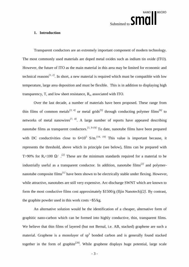
electron microscopy as shown in figure 2 C. It is clear from this image that these films consist
of a disordered array of graphitic flakes lying approximately in the plane of the film. These
flakes range in lateral size from ~100 nm to ~3 µm. While it is impossible to gauge their
thickness from these images, a number of the flakes appear significantly thicker than
monolayers suggesting that some aggregation of the graphene flakes has occurred during film
formation. However, some flakes appear partially transparent to the electron beam, suggesting
them to be relatively thin.
It is important to note that we prepare these films from dispersions of graphene[33] not
graphene oxide; measurements have shown this type of dispersion process does not introduce
significant quantities of defects or oxides to the flakes[31, 33]. Nevertheless, it is important to
confirm the absence of defects or oxides in these filtered films. We test for oxides using FTIR
as shown in figure 2E. Oxides such as C=O, -COOH or C-O groups have characteristic
features at 1000 cm-1 and 1700 cm-1 respectively. These features tend to be relatively intense
in FTIR spectra of graphene oxide films[24]. No such features are observed here. We note that
the features appearing in figure 2E in the range 600-1300 cm-1 are associated with the glass
substrate.
We can also test for the presence of structural defects using Raman spectroscopy.
Shown in figure 2F is a Raman spectrum (633 nm) for an as-produced film with the spectrum
of the starting graphite powder shown for comparison. Three bands are immediately clear; the
D band around 1300 cm-1, the G band around 1600 cm-1 and the 2D band around 2650 cm-1.
Of most interest are the D and 2D bands. The D band is indicative of the presence of defects,
which in graphene are generally divided into basal plane defects and edge defects. Previous
studies of graphene exfoliated from graphite using surfactants[33] or amide solvents[31] have
shown very small D bands which have been attributed to flake edges. In the thin film shown
here, this band is relatively intense compared to the smaller band observed in the graphite

Submitted to
- 7 -
powder. (In addition the growth of the shoulder at ~1615 cm-1 is indicative of some defect
creation.[36]) At first sight this suggests the presence of basal plane defects, possibly induced
during sonication. However, it more probably reflects the formation of new edges as flakes
are cut during sonication. In addition, we note that this band is much narrower than those
typically observed for defective CMGs[21]. Thus, while edge defects may be introduced during
sonication, the basal defect content should be much lower than that found in chemically
modified graphenes. We can also look at the 2D band. The shape of this band is indicative of
the number of monolayers per flake[37]. We note that the shape of this band for the as-
produced film is significantly different to the 2D band of graphite and is reminiscent of few
layer graphene[37]. This would suggest that although aggregation occurs during film formation,
the aggregates are not Bernal stacked but rather are randomly re-stacked. As such the films
are neither graphite nor graphene but a disordered array of few-layer graphenes, perhaps are
best classified as randomly restacked graphene.
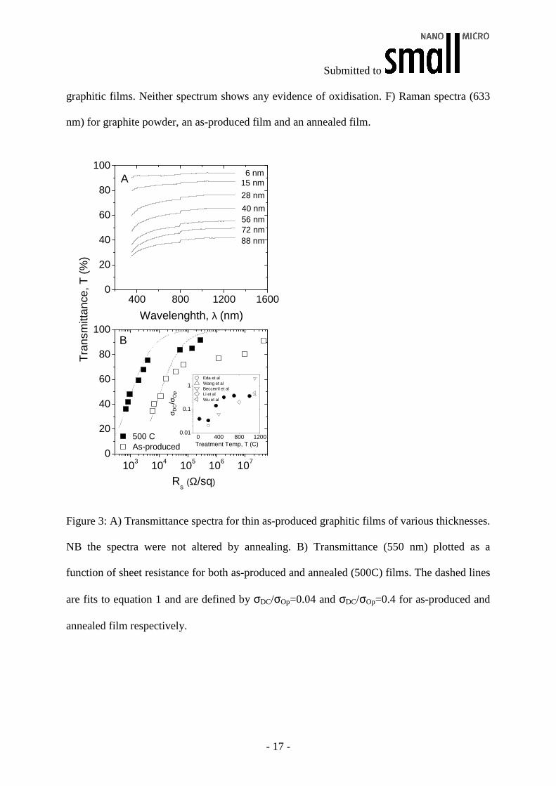
We have measured the optical and electrical properties of these as-produced graphitic
films. Shown in figure 3A are optical transmission spectra for a range of films with varying
thickness. These spectra are broad and featureless as expected for a material composed of 2-
dimensional entities. Typically the transmittance varies from ~90% to ~35% as the thickness
increases from 6 nm to 88 nm. We have measured the sheet resistance of the films to fall from
106 Ω/ to 103 Ω/ over the same range. The transmittance (550 nm) is plotted as a function
of sheet resistance in figure 3B. Here, both transmittance and sheet resistance fall off as the
film thickness increases.
In general for thin metallic films, the transmittance is related to the sheet resistance
by[38, 39]:
2
012
Op
s DC
ZT
R
σσ
−
= +
equation 1

Submitted to
- 8 -
where Z0=377 Ω is the impedance of free space and σDC and σOp are the DC and optical
conductivity respectively. This expression can be fitted to the data in figure 3B with a good fit
obtained for films with t>20 nm (deposited mass per area M/A>40 mg/m2). This fit gives a
value of σDC/σOp ~0.04 for the as-prepared films.
One can use equation 1 to estimate σDC/σOp from the data presented in the literature
for transparent films based on CMG. In all cases these films were reduced thermally with
σDC/σOp increasing with anneal temperature. For example, Eda et al produced films from
hydrazine reduced CMG which had been annealed at 200C. These films had Rs~105 Ω/ @
T~85% giving σDC/σOp = 0.02.[28] Li et al[24] exfoliated graphite with the aid of acid allowing
them to prepare films by the LB technique. These are annealed at 800oC to remove oxides,
resulting in films with σDC/σOp ~0.2 (Rs~104 Ω/ @ T~80%). Wu et al[30] spun cast CMG to
produce films which were subsequently annealed at 1100oC to give σDC/σOp ~0.5 (Rs~3500
Ω/ @ T~82%). Wang et al[29] prepared films of CMG by dip-coating followed by
annealing at 1100oC with σDC/σOp ~0.42 (Rs~1800 Ω/ @ T~64% at 550 nm (quoted data:
70% at 1000 nm)). Similarly Becerril[27] et al produced CMG films by spin coating. By using
a combination of hydrazine reduction and annealing at 400oC they achieved Rs~104 Ω/ @
T~60%, resulting in σDC/σOp ~0.06. By annealing at 1100oC they produced films with Rs~330
Ω/ @ T~60%, resulting in σDC/σOp ~2. For comparison purposes, this data is summarised in
figure 3 (inset). This makes clear that the annealed films quoted in the literature out-perform
our as-produced graphitic films. We must consider a post-treatment technique to improve the
properties.
While we have shown that our graphitic films have low defect contents compared to
CMGs, it may be advantageous to perform an annealing step. There are two reasons for this;
micromechanically cleaved graphene is generally annealed to improve electrical

Submitted to
- 9 -
performance[20] and by analogy with nanotube films, a post-treatment may remove residual
surfactant[15]. We annealed a number of films (t=40nm) in flowing H2/Ar at a range of
temperatures from 200oC to 1000oC. SEM analysis (figure 2D) shows no significant
difference in film morphology before and after annealing at 500oC. In addition FTIR and
Raman analysis (figure 2E and F) show no change in oxide or defect content. We measured Rs
and T for all annealed films, using the data to calculate σDC/σOp. As shown in fig 3B, inset,
the measured value of σDC/σOp is constant below 200oC but increases dramatically between
200oC and 500oC before levelling off above 500oC at σDC/σOp~0.35. We note from this data
that our graphitic films out-perform the reduced CMG films at all anneal temperatures below
1100oC. We then prepared films with a range of thickness, before annealing at 500oC. The
transmittances and sheet resistances are shown in figure 3B. The data fits well to equation 1
for t>20 nm with the fit giving σDC/σOp ~0.4. We note that while σDC/σOp ~0.4 is close to the
state of the art for thin films prepared from CMG, it is a long way from industrial
requirements. The minimum industry standards for a transparent conductor are T>90% for
Rs<100 Ω/ . This means the minimum acceptable value of the conductivity ratio is σDC/σOp
=35. Below, we will discuss methods to bridge this gap.
To complete our analysis we measured the thickness dependence of the film properties
for films annealed at 500oC (see SI for description of film thickness measurement). We
measured T (550 nm) and Rs as shown in figure 4A and B. Note the data for un-annealed
films are shown for comparison. As t is increased, T decreases smoothly for both film types.
For thin conducting films, the transmittance scales with thickness as[39]:
2
012 Op
ZT tσ
− = +
equation 2
This expression can be well fitted to both data sets with a value of σOp≈4.2×10⁴ S/m. When
one analyses data presented in the literature for reduced CMG films, one finds values of σOp

Submitted to
- 10 -
in the range 5-10×104 S/m, in reasonable agreement with our value[27-29]. We note that when
analysed using equation 2, Nair’s transmittance data for micromechanically cleaved graphene
suggests σOp=1.8×10⁵ S/m.[40] We suggest that the lower value recorded here reflects the
different inter-layer interactions associated with randomly restacked graphene. Shown in
figure 4B is data for Rs for each film type. While both data sets decrease with increasing film
thickness, the annealed data is significantly lower than the as-produced. In addition while both
data sets scale inversely with thickness at high thicknesses, both sets display anomalously
high sheet resistances at lower film thickness. This effect has been observed for films of both
carbon nanotubes[2] and silver nanowires[8] .
To see this more clearly we calculate the DC conductivity from σ=1/Rst, as shown in
figure 4C. Note that the conductivity ratio, σDC/σOp, is shown on the right axis. For both film
types the DC conductivity is constant for thicknesses above 20 nm. For the annealed film,
σDC=1.5×10⁴ S/m above 20 nm (σDC/σOp~0.4). Such a DC conductivity value is close to the
best data for chemically modified graphene films[41]. However for thinner films the
conductivity falls off significantly. Such behaviour is observed for other nano-structured thin
films[1, 2, 8, 14] and has previously been attributed to thickness non-uniformity at low
thickness[2, 8]. To study this, we measure the film thickness non-uniformity by measuring the
spatially resolved absorbance using a transmission scanner[2, 8]. We define the non-uniformity
as the standard deviation of absorbance divided by the mean absorbance, ∆A/A. We plot this
parameter for both film types in figure 4D. In both cases, the non-uniformity is constant for
thicknesses above 20 nm. However below t=20 nm the non-uniformity increases substantially.
We suggest that it is this increased non-uniformity which causes the reduction in conductivity
at low thicknesses. For nanotube and nanowire films, it has been suggested that the increase in
non-uniformity tends to occur for thicknesses close to twice the nanotube bundle / nanowire
diameter[2, 8]. If a similar rule applied here, it would suggest that the graphitic flakes making

Submitted to
- 11 -
up the films are typically ~10 nm in thickness. This suggests significant aggregation has
occurred during film formation.
We note that the uniformity is better in the annealed samples. To test this further we
performed atomic force microscopy on a number of our films (see supporting information).
Such images showed graphitic flakes of sizes similar to those in the SEM images. These
flakes displayed a range of heights from a few nm to 10s of nm. We measured the root mean
square roughness for films before and after annealing finding values of ~13 nm and ~11 nm
respectively. The films after annealing were consistently about 20% less rough suggesting that
some re-organisation occurs during annealing.
Nano-structured, thin, transparent films are most likely to be used in e-paper type
applications. Thus they must retain their conductivity under flexing. We monitored the film
conductivity under both tensile and compressive bending for two graphitic films on PET of
thickness 40 nm and 88 nm as shown in figure 5. During the first bend cycle (insets) the
resistance increased slightly for the films in tension. The compressively bent films displayed
more complex behaviour but varied by no more than 6% from the initial resistance. We also
plot the mean sheet resistance per cycle for both films. In each case the resistance falls
slightly over 2000 cycles. We note that none of the films failed. Rather the measurement was
limited by time constraints.
3. Conclusion
We have demonstrated the preparation of thin transparent films of graphene. The
electrical stability coupled with the high levels of transparency observed and the low cost of
graphite make these films attractive as transparent conductors. However, like CMG based
films, these films have DC conductivity much too low for practical purposes. In addition, the

Submitted to
- 12 -
need to anneal is a big disadvantage. However, they do have some significant advantages over
CMG based films. Most importantly, the flakes are graphene at all stages, there is no need to
oxidise or reduce. Because of this, the requirement to anneal is not intrinsic. We suspect it
aids removal of residual surfactant and facilitates some rearrangement of graphene sheets. We
believe that such effects can be achieved by improving the dispersion or film formation
process, perhaps by washing or acid treatment (mild enough not to oxidise the graphene). In
addition, these films have much lower defect contents compared to CMG films. This means
the ultimate conductivity of these films is likely to be much higher. Finally, these films
consist of large aggregates which contribute to roughness and provide the ultimate limit to
conductivity. Improvements in the dispersion or film formation procedures will reduce this
aggregation leading to better quality films with much higher DC conductivities. In contrast
CMG films display much less aggregation. This means they have much less scope for
improvement. We believe further improvement is possible which could see these films
supersede carbon nanotube films as the heirs to ITO.
4. Experimental Section
Graphite was purchased from Branwell Graphite Ltd (Branwell natural graphite, grade
2369, www.branwell.u-net.com/, typical cost $5/kg) while sodium cholate surfactant was
purchased from Aldrich. Both products were used as supplied. A stock solution of sodium
cholate (SC) (5mg/ml) was prepared by stirring overnight in Millipore water. This was
subsequently diluted for further use. Graphite (initial concentration 0.75mg/ml) was dispersed
in 25 ml SC solution (concentration 0.5mg/ml) by sonication for 140 mins in a low power
ultrasonic bath (Branson 1510E-MT bath sonicator). The resulting dispersion was left to stand
for 24hrs to allow any unstable aggregates to form. The top 80% of the dispersion was
decanted and discarded. SC was then added to maintain the starting volume of dispersion at
Submitted to
- 13 -
25ml. This was then sonicated for a further 140mins. Again the dispersion was left to stand
overnight and then centrifuged at 5000rpm for 90min (Hettich Mikro 22R). After
centrifugation the top 80% of supernatant was decanted and retained for use. The post
centrifuge graphene concentration was estimated from absorbance measurements (Varian
Cary6000i) using the measured extinction coefficient of graphene in surfactant water
solutions (1390 ml mg-1 m-1)[33].
The resulting dispersions were vacuum filtered using porous cellulose filter
membranes (MF-Millipore membrane, mixed cellulose esters, hydrophilic, 0.025µm 47 mm)
to give thin graphitic films. The thickness of these films was controlled by the volume of
dispersion filtered, and hence the deposited graphene mass. The deposited films were then
transferred onto glass slides using iso-propanol to remove trapped air between the film and
substrate thus improving adhesion. The cellulose filter membrane was then removed by
treatment with acetone vapour and subsequent acetone liquid baths followed by a methanol
bath[19]. The final film diameter was 36 mm. The film thickness, t, was measured by AFM
(see supporting information). Films were annealed at various temperatures under H2/Ar flow
for 2hrs.
Optical transmission spectra were recorded before and after anneal using a Varian
Cary 6000i. In all cases, a glass slide was used as the reference. Sheet resistance
measurements were made before and after anneal using the four-probe technique with silver
electrodes of dimensions and spacings typically of ~mm size and a Keithley 2400 source
meter. Transmission scans were made using an Epson Perfection V700 photo flat-bed
transmission scanner with a bit depth of 48 bits per pixel and a spatial resolution of 6400
dpi.[2] TEM samples were prepared by pipetting a few milliliters of this dispersion onto holey
carbon mesh grids (400 mesh). Bright-field TEM images were taken with a Jeol 2100,
operated at 200 kV. Scanning electron microscopy measurements were made using a Zeiss

Submitted to
- 14 -
Ultra plus SEM. Raman spectra were taken on a Horiba Jobin Yvon LabRAM-HR using a
100× objective lens with a 633 nm laser excitation. Attenuated total reflectance FTIR spectra
of these films were taken on a Perkin-Elmer Spectrum 100. AFM measurements for surface
roughness and thickness were taken with a Digital Instruments Nanoscope IIIA from Veeco
Systems in tapping mode using silicon tips with a resonance frequency of 320 kHz.
Electromechanical measurements were made using a Zwick Z0.5 Proline tensile tester as
described previously[1, 2].
Acknowledgments
The authors acknowledge Science Foundation Ireland through the principle investigators
scheme for supporting this work.

Submitted to
- 15 -
Figures
Figure 1: A) Photograph of a water/sodium cholate graphene dispersion before (left) and after
(right) centrifugation. B) & C) TEM images of graphene flakes deposited from sodium
cholate stabilized aqueous graphene dispersions. A) A folded monalayer. B) An aggregate
containing a folded ribbon.
A B C
500 nm 500 nm

Submitted to
- 16 -
Figure 2: A) and B) Photographs of graphitic films on PET (thicknesses of 6 nm and 40 nm
respectively). C) and D) SEM images of 72 nm thick graphitic films before and after
annealing at 500 oC respectively. E) ATR-FTIR spectra for both as-produced and annealed
1000 1500 2000 2500 3000
Inte
nsity
(au
)
Graphite powder
500 C anneal
Raman shift (cm-1)
D G
2D
As-produced
F
4000 3000 2000 100080
85
90
95
100
500 C
Tra
nsm
issi
on (
%)
Wavenumber (cm-1)
Glass
As-produced
E
A B
C D
200 nm 200 nm
Submitted to
- 17 -
graphitic films. Neither spectrum shows any evidence of oxidisation. F) Raman spectra (633
nm) for graphite powder, an as-produced film and an annealed film.
103 104 105 106 1070
20
40
60
80
100
0 400 800 12000.01
0.1
1
500 C As-produced
Rs (Ω/sq)
Eda et al Wang et al Beccerril et al Li et al Wu et al
Treatment Temp, T (C)
σD
C/σ
Op
400 800 1200 16000
20
40
60
80
100
15 nm
B
Tra
nsm
ittan
ce, T
(%
)
Wavelenghth, λ (nm)
A6 nm
28 nm
40 nm56 nm72 nm88 nm
Figure 3: A) Transmittance spectra for thin as-produced graphitic films of various thicknesses.
NB the spectra were not altered by annealing. B) Transmittance (550 nm) plotted as a
function of sheet resistance for both as-produced and annealed (500C) films. The dashed lines
are fits to equation 1 and are defined by σDC/σOp=0.04 and σDC/σOp=0.4 for as-produced and
annealed film respectively.

Submitted to
- 18 -
0 40 80 1200.0
0.5
1.0
10-4
10-3
10-2
10-1
100
10 1000.0
0.2
0.4
Film thickness, t (nm)
non-
unifo
rmity
,∆A
/A
101
102
103
104
500 C As-produced
σ DC (
S/m
)
104
106
108
Rs(
Ω/s
q)
0
25
50
75
100
σDC
=1.5*104 S/m
A
D
C
T (
%)
B
σOp
=4.2*104 S/m
T-1
/2-1
t (nm)
σ DC/σ
Op
Figure 4: Optical, electrical and uniformity data for as-produced and annealed (500C) films.
A) Transmittance (550 nm) plotted as a function of film thickness. The dashed line is a fit to
equation 2 and is defined by σOp=4.2×10⁴ S/m. Inset: The same data is plotted to illustrate the
applicability of equation 2. B) Sheet resistance as a function of thickness. The dashed line
illustrates bulk behaviour. C) DC conductivity plotted versus film thickness. Note that the DC
conductivity falls off below t=20 nm. The right axis denotes σDC/σOp. D) Film non-uniformity
plotted versus film thickness. The non-uniformity is defined as the standard deviation of a set
of spatially resolved absorbance measurements divided by the mean absorbance.

Submitted to
- 19 -
0
10
20
0.02 0.04 0.06 0.085.8
6.0
6.2
6.4
0.02 0.04 0.06 0.0815
16
17
18
Compression
B
Mea
n R
s per
cyc
le (
kΩ/s
q)
Tension
A
1 10 100 10000
2
4
6
t=88 nm
Cycle number
t=40 nm
Rs (
kΩ/s
q)
Strain, ε
Strain, ε
Rs
(kΩ
/sq)
Figure 5: Sheet resistance during bending for as-produced films deposited on PET.
Measurements were made for films both in tension and compression. Data for A) a 40 nm
thick film and B) an 88 nm thick film. Inset: Resistance versus strain for the first cycle. Main
graph: Mean resistance per cycle versus cycle number

Submitted to
- 20 -
References
[1] S. De, P. E. Lyons, S. Sorrel, E. M. Doherty, P. J. King, W. J. Blau, P. N. Nirmalraj, J. J. Boland, V. Scardaci, J. Joimel, J. N. Coleman, ACS Nano 2009, 3, 714. [2] E. M. Doherty, S. De, L. Lyons, A. Shmelov, P. N. Nirmalraj, V. Scardaci, W. J. Blau, J. J. Boland, J. N. Coleman, Carbon 2009, 47, 2466. [3] J. Meiss, M. K. Riede, K. Leo, Applied Physics Letters 2009, 94, 013303 [4] B. O'Connor, C. Haughn, K. H. An, K. P. Pipe, M. Shtein, Applied Physics Letters 2008, 93, 223304. [5] M. G. Kang, M. S. Kim, J. S. Kim, L. J. Guo, Advanced Materials 2008, 20, 4408. [6] Y. H. Zhou, F. L. Zhang, K. Tvingstedt, S. Barrau, F. H. Li, W. J. Tian, O. Inganas, Applied Physics Letters 2008, 92, 233308. [7] J. Y. Lee, S. T. Connor, Y. Cui, P. Peumans, Nano Letters 2008, 8, 689. [8] S. De, T. Higgins, P. E. Lyons, E. M. Doherty, P. N. Nirmalraj, W. J. Blau, J. J. Boland, J. N. Coleman, ACS Nano 2009, 3, 1767. [9] C. M. Aguirre, S. Auvray, S. Pigeon, R. Izquierdo, P. Desjardins, R. Martel, Applied Physics Letters 2006, 88, 183104 [10] E. Artukovic, M. Kaempgen, D. S. Hecht, S. Roth, G. GrUner, Nano Letters 2005, 5, 757. [11] T. M. Barnes, J. V. de Lagemaat, D. Levi, G. Rumbles, T. J. Coutts, C. L. Weeks, D. A. Britz, I. Levitsky, J. Peltola, P. Glatkowski, Physical Review B 2007, 75, 235410. [12] T. M. Barnes, X. Wu, J. Zhou, A. Duda, J. van de Lagemaat, T. J. Coutts, C. L. Weeks, D. A. Britz, P. Glatkowski, Applied Physics Letters 2007, 90, 243503. [13] M. A. Contreras, T. Barnes, J. van de Lagemaat, G. Rumbles, T. J. Coutts, C. Weeks, P. Glatkowski, I. Levitsky, J. Peltola, D. A. Britz, Journal of Physical Chemistry C 2007, 111, 14045. [14] H. Z. Geng, K. K. Kim, K. P. So, Y. S. Lee, Y. Chang, Y. H. Lee, Journal of the American Chemical Society 2007, 129, 7758. [15] H. Z. Geng, D. S. Lee, K. K. Kim, G. H. Han, H. K. Park, Y. H. Lee, Chemical Physics Letters 2008, 455, 275. [16] G. Gruner, Journal of Materials Chemistry 2006, 16, 3533. [17] M. Kaempgen, G. S. Duesberg, S. Roth, Applied Surface Science 2005, 252, 425. [18] B. B. Parekh, G. Fanchini, G. Eda, M. Chhowalla, Applied Physics Letters 2007, 90, 121913. [19] Z. C. Wu, Z. H. Chen, X. Du, J. M. Logan, J. Sippel, M. Nikolou, K. Kamaras, J. R. Reynolds, D. B. Tanner, A. F. Hebard, A. G. Rinzler, Science 2004, 305, 1273. [20] A. K. Geim, K. S. Novoselov, Nature Materials 2007, 6, 183. [21] S. Stankovich, D. A. Dikin, R. D. Piner, K. A. Kohlhaas, A. Kleinhammes, Y. Jia, Y. Wu, S. T. Nguyen, R. S. Ruoff, Carbon 2007, 45, 1558. [22] S. Stankovich, D. A. Dikin, G. H. B. Dommett, K. M. Kohlhaas, E. J. Zimney, E. A. Stach, R. D. Piner, S. T. Nguyen, R. S. Ruoff, Nature 2006, 442, 282. [23] D. A. Dikin, S. Stankovich, E. J. Zimney, R. D. Piner, G. H. B. Dommett, G. Evmenenko, S. T. Nguyen, R. S. Ruoff, Nature 2007, 448, 457. [24] X. L. Li, G. Y. Zhang, X. D. Bai, X. M. Sun, X. R. Wang, E. Wang, H. J. Dai, Nature Nanotechnology 2008, 3, 538. [25] S. Park, J. H. An, I. W. Jung, R. D. Piner, S. J. An, X. S. Li, A. Velamakanni, R. S. Ruoff, Nano Letters 2009, 9, 1593. [26] G. Eda, G. Fanchini, M. Chhowalla, Nature Nanotechnology 2008, 3, 270.

Submitted to
- 21 -
[27] H. A. Becerril, J. Mao, Z. Liu, R. M. Stoltenberg, Z. Bao, Y. Chen, Acs Nano 2008, 2, 463. [28] G. Eda, Y. Y. Lin, S. Miller, C. W. Chen, W. F. Su, M. Chhowalla, Applied Physics Letters 2008, 92, 233305. [29] X. Wang, L. J. Zhi, K. Mullen, Nano Letters 2008, 8, 323. [30] J. B. Wu, H. A. Becerril, Z. N. Bao, Z. F. Liu, Y. S. Chen, P. Peumans, Applied Physics Letters 2008, 92, 263302. [31] Y. Hernandez, V. Nicolosi, M. Lotya, F. M. Blighe, Z. Y. Sun, S. De, I. T. McGovern, B. Holland, M. Byrne, Y. K. Gun'ko, J. J. Boland, P. Niraj, G. Duesberg, S. Krishnamurthy, R. Goodhue, J. Hutchison, V. Scardaci, A. C. Ferrari, J. N. Coleman, Nature Nanotechnology 2008, 3, 563. [32] P. Blake, P. D. Brimicombe, R. R. Nair, T. J. Booth, D. Jiang, F. Schedin, L. A. Ponomarenko, S. V. Morozov, H. F. Gleeson, E. W. Hill, A. K. Geim, K. S. Novoselov, Nano Letters 2008, 8, 1704. [33] M. Lotya, Y. Hernandez, P. J. King, R. J. Smith, V. Nicolosi, L. S. Karlsson, F. M. Blighe, S. De, Z. M. Wang, I. T. McGovern, G. S. Duesberg, J. N. Coleman, Journal of the American Chemical Society 2009, 131, 3611. [34] T. Hertel, A. Hagen, V. Talalaev, K. Arnold, F. Hennrich, M. Kappes, S. Rosenthal, J. McBride, H. Ulbricht, E. Flahaut, Nano Letters 2005, 5, 511. [35] Z. Sun, V. Nicolosi, D. Rickard, S. D. Bergin, D. Aherne, J. N. Coleman, Journal of Physical Chemistry C 2008, 112, 10692. [36] L. M. Malard, M. A. Pimenta, G. Dresselhaus, M. S. Dresselhaus, Physics Reports-Review Section of Physics Letters 2009, 473, 51. [37] A. C. Ferrari, J. C. Meyer, V. Scardaci, C. Casiraghi, M. Lazzeri, F. Mauri, S. Piscanec, D. Jiang, K. S. Novoselov, S. Roth, A. K. Geim, Physical Review Letters 2006, 97, 187401. [38] L. Hu, D. S. Hecht, G. Gruner, Nano Letters 2004, 4, 2513. [39] M. Dressel, G. Gruner, Electrodynamics of Solids: Optical Properties of Electrons in Matter, Cambridge University Press, Cambridge 2002. [40] R. R. Nair, P. Blake, A. N. Grigorenko, K. S. Novoselov, T. J. Booth, T. Stauber, N. M. R. Peres, A. K. Geim, Science 2008, 320, 1308. [41] S. Park, R. S. Ruoff, Nat Nano 2009, 4, 217.

Submitted to
- 22 -
TOC
Graphene thin films are prepared using surfactant stabilized dispersions of graphene in water.
Electromechanical stability coupled with high transparency make these films attractive as
transparent flexible conductors.
500 nm