Embed Size (px)
Citation preview

PROGRESS REPORT
1903558 (1 of 32) © 2019 WILEY-VCH Verlag GmbH & Co. KGaA, Weinheim
www.advmat.de
Flexible Neuromorphic Electronics for Computing, Soft Robotics, and Neuroprosthetics
Hea-Lim Park, Yeongjun Lee, Naryung Kim, Dae-Gyo Seo, Gyeong-Tak Go, and Tae-Woo Lee*
DOI: 10.1002/adma.201903558
and the challenges of the von Neumann bottleneck.[1] For information processing, classical von Neumann-based com-puting systems depend on centralized and sequential operations with a clock cycle, while biological nervous systems are based on distributed, parallel, and event-driven operations.[2,3] As a solution for efficient processing of large quanti-ties of complex data, the concept of the neuromorphic electronics which emu-late the functions and the information processing of biological nervous systems has emerged.[4,5] Synapses in such sys-tems combine processing and memory, so they avoid the von Neumann bottleneck,[6] and can modulate information flow, data processing, and memory function by changing the synaptic weight.[7,8] Thus, implementation of synaptic behaviors in neuromorphic electronics presents a next-generation computing paradigm.
The biological nervous systems in ver-tebrates are largely divided into the central nervous system (CNS, i.e., the brain and the spinal cord) and the peripheral nervous system (PNS, i.e., sensory nerves
and motor nerves).[9] The CNS performs computing, learning, and memorizing activities, and manages the activity of the body in response to information received from the PNS. The PNS perceives and responds to stimuli such as light, sound, pres-sure, and chemicals, and relays this information between the CNS and the rest of the body.
Neuromorphic electronics that emulate the functions of the CNS and the PNS could realize computing, soft robotics, and neuroprosthetics (Figure 1). Construction of artificial CNSs and PNSs requires development of functional synaptic devices in which information processing capability is merged with various functions such as detection of stimuli (e.g., light, pres-sure, chemical analytes) and reaction to environment. Further, these artificial synapses need to be integrated on a system level. Implementation of artificial nervous systems in prosthetics and soft robots requires devices that are mechanically flexible and stretchable (Figure 1). Biological bodies are composed of many curved surfaces with arbitrary shapes, so mechanical flexibility enables integration of artificial nerves with bodies such as organs, nervous systems, and skins, and this inte-gration guarantees signal transfer.[10,11] Movement of a body involves both bending and stretching forces.[12] For example, knees undergo up to 55% of stretching during movement.[13]
Flexible neuromorphic electronics that emulate biological neuronal systems constitute a promising candidate for next-generation wearable computing, soft robotics, and neuroprosthetics. For realization, with the achievement of simple synaptic behaviors in a single device, the construction of artificial synapses with various functions of sensing and responding and integrated systems to mimic complicated computing, sensing, and responding in biological systems is a prerequisite. Artificial synapses that have learning ability can perceive and react to events in the real world; these abilities expand the neuromorphic applications toward health monitoring and cybernetic devices in the future Internet of Things. To demonstrate the flexible neuromorphic systems successfully, it is essential to develop artificial synapses and nerves replicating the functionalities of the biological counterparts and satisfying the requirements for constructing the elements and the integrated systems such as flexibility, low power consumption, high-density integration, and biocompatibility. Here, the progress of flexible neuromorphic electronics is addressed, from basic backgrounds including synaptic characteristics, device structures, and mechanisms of artificial synapses and nerves, to applications for computing, soft robotics, and neuroprosthetics. Finally, future research directions toward wearable artificial neuromorphic systems are suggested for this emerging area.
Neuromorphic Electronics
Dr. H.-L. Park, Dr. Y. Lee, N. Kim, D.-G. Seo, G.-T. Go, Prof. T.-W. LeeDepartment of Materials Science and EngineeringSeoul National University1 Gwanak-ro, Gwanak-gu, Seoul 08826, Republic of KoreaE-mail: [email protected], [email protected]. Y. Lee, Prof. T.-W. LeeBK21 PLUS SNU Materials Division for Educating Creative Global LeadersSeoul National University1 Gwanak-ro, Gwanak-gu, Seoul 08826, Republic of KoreaProf. T.-W. LeeInstitute of Engineering Research Research Institute of Advanced MaterialsNano Systems Institute (NSI)Seoul National University1 Gwanak-ro, Gwanak-gu, Seoul 08826, Republic of Korea
The ORCID identification number(s) for the author(s) of this article can be found under https://doi.org/10.1002/adma.201903558.
1. Introduction
With the spread of Internet of Things (IoT) and artificial intel-ligence (AI), dataset sizes have exploded, facing the limitations in energy efficiency with approaching the end of Moore’s law
Adv. Mater. 2020, 32, 1903558

© 2019 WILEY-VCH Verlag GmbH & Co. KGaA, Weinheim1903558 (2 of 32)
www.advmat.dewww.advancedsciencenews.com
To emulate biological movement closely, devices must allow movement of the joints that is constrained only as desired.[14–16] With the rapidly growing needs toward wearable and implant-able electronics, the development of flexible and stretchable neuromorphic electronics that has been focused on health monitoring can be extended to robots, exoskeletons, cyber-netic devices, brain–computer interfaces, and transmission of sensorimotor neural signals. Despite the importance of flexible neuromorphic electronics, the direction and goals for research have not been sufficiently discussed.
Here, we review recent progress in development of flexible neuromorphic electronics, and provide guidelines for future research toward development of brain-inspired computing, soft robotics, and neuroprosthetics. First, we present basic background about biological synapses and various synaptic characteristics which should be emulated by artificial synapses. Second, together with device structures and mechanisms of artificial synapses, we will cover the requirements of flexible devices for actual applications including flexibility, low power consumption, high-density integration, and biocompatibility. Then, we will present examples of applications for brain-inspired computing, soft robotics, and neuroprosthetics at a unit cell level and at a system level. Finally, we will suggest future research directions toward wearable artificial neuromor-phic electronics.
2. Biological Synapses and Synaptic Properties
The human brain is a massively parallel computing structure that processes input information by synaptic transmission and
consumes only around 1–10 fJ per synaptic event.[17,18] The neural network is composed of ≈1012 neurons and ≈1015 syn-apses and propagates neural signals in the CNS and the PNS. The PNS consists of sensory neurons that send information to the CNS for processing, and that activate motor effectors.
Synapses are categorized into electrical synapses and chemical synapses. Electrical synapses transmit signals bidi-rectionally at gap junctions that are electrically coupled across
Tae-Woo Lee is a professor in the department of Materials Science and Engineering (MSE) at Seoul National University, South Korea. He received his Ph.D. in chemical engineering from KAIST, South Korea in 2002. He joined Bell Laboratories, USA, as a postdoctoral researcher and worked at Samsung Advanced Institute
of Technology as a member of research staff (2003–2008). He was an associate professor in MSE at Pohang University of Science and Technology (POSTECH), South Korea, until August 2016. His research focuses on printed electronics based on organic and organic–inorganic hybrid materials for flexible displays, solid-state lighting, solar energy conversion devices, and bioinspired neuromorphic devices.
Adv. Mater. 2020, 32, 1903558
Figure 1. Flexible neuromorphic electronics for neuromorphic computing, humanoid robotics, and neuroprosthetics. These applications require functionality, high-density integration, low power consumption, flexibility, and biocompatibility. Artificial parts of (A′) and (B′) indicate pressure sensor and artificial synapse, respectively, which correspond to biological counterparts’ mechanoreceptor under skin (A) and biological synapses (B).

© 2019 WILEY-VCH Verlag GmbH & Co. KGaA, Weinheim1903558 (3 of 32)
www.advmat.dewww.advancedsciencenews.com
a narrow synapse (≈3 nm).[19] Chemical synapses transfer information when a presynaptic neuron releases neuro-transmitters into a synaptic cleft with a gap of 20–50 nm that separates the presynaptic neuron from a postsynaptic neuron (Figure 2a,b). The synaptic strength of a chemical synapse is delicately controlled by the relative importance of input information, so chemical synapses mainly contribute to learning or memorizing functions.[20–22] When the elec-tric signals of an action potential arrive at the axon terminal of presynaptic neuronal membrane (Figure 2b, ①), then Ca2+ ion channels are opened and Ca2+ ions rush into the neu-ronal membrane ②. The influx of Ca2+ ions makes synaptic vesicles migrate to the terminal ③, where they release neu-rotransmitters from synaptic vesicles ④.[23] Then, the neuro-transmitters bind to receptors on the postsynaptic neuronal membrane (soma or dendrite), and thereby trigger opening of ion channels ⑤. With cell membranes, the concentration gradients of several ions, mainly K+, Na+, and Cl−, are sepa-rately distributed.[22–24] K+ ions are more concentrated within neurons, whereas the Na+ and Cl− are more concentrated in the extracellular medium; this gradient of chemical concentration induces formation of a potential difference across the neural membrane.[25] The intracellular potential is usually negative
relative to the extracellular medium, and the membrane potential is ≈−70 mV, which is called the resting potential.[25]
The membrane potential changes in response to activation of ion channels by various neurotransmitters, and synapses can either be excitatory or inhibitory by the combination of neurotransmitters and ion channels. In excitatory synapses, the membrane potential becomes depolarized by the influx of Na+ ions through activated Na+ ion channels; this change in potential is called the excitatory postsynaptic potential (EPSP) (Figure 2c, blue lines).[26] In inhibitory synapses, the mem-brane potential becomes negatively hyperpolarized by an influx of Cl− ions through Cl− ion channels, and causes an inhibitory postsynaptic potential (IPSP) (Figure 2c, red lines).[26] Multiple postsynaptic potentials (PSPs) are integrated at the axon hillock which is the initial portion of axon from the soma (Figure 2c(i)). When the sum of EPSP and IPSP exceeds a threshold, the neu-ronal membrane becomes positively charged, and generates a new action potential toward the axon terminal which can transmit the signal to another cell (Figure 2c(ii)).[22,27] The syn-aptic integration of signals can be spatial or temporal.[28] Spatial summation integrates PSPs from many synapses on the same neuron simultaneously. Temporal summation integrates suc-cessive PSPs that occur within 1–15 ms at the same synapse.[29]
Adv. Mater. 2020, 32, 1903558
Figure 2. a) Schematic illustration of neuron structures.[18] b) Structure and components of the chemical synapse.[22] c) Postsynaptic potential summation at the axon hillock.[28] Part (i) shows multiple PSPs of EPSP and IPSP added at the axon hillock (signal integration). Part (ii) shows generation of a new action potential when the sum of PSPs exceeds a threshold. d) Topological changes of neurons (recruitment of new neurotransmitter receptors on Synapse A, and formation of new synapses of Synapse B) by repeated stimulations.[23,38] e) Graphs of long-term plasticity in the hippocampus.[37] Top panel shows LTP by high-frequency spikes (usually 100 Hz) and bottom panel demonstrates LTD by low-frequency stimulation (usually less than 1 or 5 Hz). f) Four types of STDP forms widely emulated by artificial synapses.[46–50]

© 2019 WILEY-VCH Verlag GmbH & Co. KGaA, Weinheim1903558 (4 of 32)
www.advmat.dewww.advancedsciencenews.com
Synaptic plasticity is a change in synaptic strength (synaptic weight) in response to action potentials; it is an important property of neurons that enables learning and memory.[23,30,31] It can be classified into short-term plasticity (temporary change of synaptic weight) and long-term plasticity (long change of synaptic weight); both types can have potentiation (increasing) and depression (decreasing) states.[32,33] During potentiation, the amplitude of the postsynaptic potential increases; the result is an increase in the number of action potentials that can be generated by the same number of stimulations. When IPSPs counteract EPSPs, depression occurs; the result is an increase in the number of stimulations that are required to make the same number of action potentials as before. When action potentials are repetitive, relatively frequent, or both, they cause increase in the quantity of neurotransmitters toward the postsynapse membrane, so influx of Ca2+ ions increases in the postneuron; the result is short-term potentiation (STP). By contrast, weak or infrequent action potentials along the pre-neuron axons result in short-term depression (STD) of the synapses.[34] STP and STD can be represented as paired-pulse facilitation (PPF) and paired-pulse depression (PPD), respec-tively.[35] During STP, increased Ca2+ influx in the postneurons leads to an increase in the receptor concentration and more neurotransmitters can be received by the increased receptors. Thus, each PSP becomes higher than the previous PSP when the postneuron receives the same number of chemical signals; this response is called PPF.[34,36] PPD is caused from reduced influx of Ca2+ ions (weak or infrequent action potentials), i.e., STD. The receptor concentration decreases, so each PSP is weaker than the previous one on the postneuron. Repeated or frequent stimulations for a long time induce topological changes in neurons; these changes can result in conversion of short-term plasticity (including STP and STD) to long-term plasticity (Figure 2d).[37] When the concentration of Ca2+ ions exceeds a threshold, biosignals are triggered, which results in synthesis of RNAs that encode proteins to form new synapses. This results in a persistent strengthening of synapses which is called long-term potentiation (LTP) (Figure 2e, top panel).[37,38] By contrast, when the frequency of action potentials is low, the number of synapses and receptors decreases; this phe-nomenon is called long-term depression (LTD) (Figure 2e, bottom panel).[37,39] STP is involved in various computations, working memory, and short-term memory (seconds to hours); LTP is involved in learning and long-term memory (hours to months).
The spike rate and the timing between paired spikes have been reported as the main factors that induce modification of synaptic weight in biological neural networks (Figure 2f). Syn-aptic information is encoded as spike-based action potentials with the same amplitude, so the plasticity is mainly affected by the frequency of spikes; this effect is defined as spike rate–dependent plasticity (SRDP).[40–42] To stimulate neurons, many researchers have applied AC signals or pulse trains to observe the responses at various frequencies.[43] Markram found that EPSPs depend on the frequency at neocortical pyramidal neurons[40] and O’Dell and Kandel reported that low-fre-quency stimulation (5 Hz) induces depression before and after LTP states at the first region (CA1) in the hippocampal circuit of hippocampal neurons in adult pigs.[41] Dudek and
Bear showed that 3 Hz trains triggered depression but 10 Hz trains did not have any significant change and 50 Hz trains generated potentiation in the CA1 of adult rat hippocampal neurons.[42]
The temporal relationship between pre- and postsynaptic firing can also modify synaptic weight; this effect may be the basic principle of Hebbian learning.[44] Spike timing–dependent plasticity (STDP) is the phenomenon by which time interval between two spikes and their temporal order affect the synaptic weight. STDP has been regarded as a learning rule in the brain, and has been examined by varying the spike time difference ΔTpre-post = tpre − tpost where tpre and tpost are arrival times of pre- and postsynaptic spikes, respectively.[45] The first characteriza-tion of STDP was investigated by Bi and Poo through a pair of pre- and postsynaptic potentials to stimulate hippocampal neurons in rats; the results demonstrated that the magnitude of PSPs could be controlled by adjusting the timing between two spikes.[46] Postsynaptic spikes that were triggered after presynaptic spikes within 20 ms (ΔTpre-post < 0) led to potentia-tion, whereas postsynaptic spiking within 20 ms before presyn-aptic spikes (ΔTpre-post > 0) induced depression. The magnitude of LTP and LTD increased, when ΔTpre-post approached 0. Four types of STDP have been widely emulated by artificial synapses (Figure 2f).[45–50]
3. Flexible Artificial Synapses
3.1. Emulation of Biological Behaviors
Many studies have attempted to emulate a brain’s synaptic plas-ticity and functions such as memory, learning, and cognition. Artificial synapses modulate the conductances of active layers; this process is analogous to modulating synaptic weights of neurons in biological systems. In artificial synapses, the con-ductance is generally measured from the current between two electrodes (bottom and top electrodes for two-terminal (2-T) devices and source (S) and drain (D) electrodes for three-terminal (3-T) devices). Artificial synapses use electrical voltage pulses to simulate an action potentials in neurons. Application of one brief voltage pulse stimulates a momen-tary increase in current (excitatory postsynaptic currents, EPSCs) which then decays to the initial current in a short time (within a few seconds); this phenomenon is analogous to STP (Figure 3a).[9,51–54] On the contrary, application of spikes with sufficiently high amplitude, high frequency, or large number, stimulates a long-term increase in currents (hours or longer); this phenomenon is analogous to LTP (Figure 3b).[7,55,56]
STP and STD affect synaptic weights in ways that emu-late the facilitation and depression properties of biological synapses.[7] STP and STD are represented by PPF and PPD, respectively, which are induced by two consecutive spikes that occur separated by a time interval Δt. When decrease in Δt increases the amplification of the second postsynaptic current, the response is PPF, whereas when decrease in Δt decreases the second postsynaptic current, the response is PPD. PPF and PPD are usually defined as 100 × A2/A1, where A1 and A2 are the peaks of the first and the second synaptic currents, respec-tively (Figure 3c).[57,58] In PPF, the first spike increases the
Adv. Mater. 2020, 32, 1903558

© 2019 WILEY-VCH Verlag GmbH & Co. KGaA, Weinheim1903558 (5 of 32)
www.advmat.dewww.advancedsciencenews.com
postsynaptic current (EPSC), then, before the increased current has decayed completely to the original state, the second spike is applied; it induces a higher current than the first spike. PPD is the inverse reaction, in which the second voltage spikes reduces the current that is induced by the first spike. The intensity of facilitation or depression depends on Δt.
In biological synapses, ΔTpre-post finely modulates synaptic weights (STDP). This behavior can be emulated in artificial synapses, when their synaptic weights can be controlled by adjusting ΔTpre-post. Artificial synapses emulate diverse forms of STDP that occur in various parts of a brain (e.g., hippocampus, neocortex, visual cortex). One of the common STDP forms is the Hebbian STDP behavior shown as the following equation[59–62]
wA e T A
B e T B
T t
T t
0, 0
0, 0
/pre-post
/pre-post
pre-post
pre-post∆ =
⋅ ∆ ≤ >⋅ ∆ > <
− ∆
− ∆ (1)
where w is the synaptic weight, and A and B are learning rates. In Hebbian STDP, the synaptic weight is modulated by the time interval and the temporal order between pre- and postsynaptic
spikes (ΔTpre-post). w increases when the presynaptic spike fires a short time before the postsynaptic spike (ΔTpre-post ≤ 0), whereas w decreases when the presynaptic spike fires briefly after the postsynaptic spike (ΔTpre-post > 0). Artificial synapses have demonstrated Hebbian STDP and other forms of STDP such as anti-Hebbian STDP, symmetrical STDP, and visual STDP (Figure 3d).[63,64] The STDP learning rule suggests that learning is dependent on the temporal relationship between two spikes that have fixed amplitude. However, to demonstrate various STDP behaviors, many studies have focused on manipulating the spike forms (Figure 3d). These approaches inevitably require complex circuits to generate various spike forms with various ΔTpre-post, so the actual applications are limited, and effort should be devoted to achieve emulation of STDP learning rules in which ΔTpre-post alone modulates synaptic weight.
In biological systems, synaptic weights can be modulated by spiking rate. This is called SRDP or spike frequency–dependent plasticity. In SRDP, strengthening or weakening of synaptic weights, i.e., gain in postsynaptic current (PSC), is widely defined as An/A1, where An and A1 are the synaptic weights of the nth peak and the first, respectively, and this parameter relies
Adv. Mater. 2020, 32, 1903558
Figure 3. a–c) Graphs of EPSC (a), LTP (b), and PPF and PPD index over various spike time intervals (c), and d) pre- and postsynaptic spike forms (left) and the corresponding STDP forms (right) in artificial synapses. a,b) Reproduced with permission.[55] Copyright 2016, The Authors, published by American Association for the Advancement of Science. Reprinted/adapted from ref. [55]. © The Authors, some rights reserved; exclusive licensee American Association for the Advancement of Science. Distributed under a Creative Commons Attribution NonCommercial License 4.0 (CC BY-NC) http://creativecommons.org/licenses/by-nc/4.0/. c) Reproduced with permission.[35] Copyright 2017, American Institute of Physics. d) Reproduced with permission.[64] Copyright 2018, Wiley-VCH.

© 2019 WILEY-VCH Verlag GmbH & Co. KGaA, Weinheim1903558 (6 of 32)
www.advmat.dewww.advancedsciencenews.com
on spike rate.[65,66] SRDP in artificial synapses shows filtering behaviors (Figure 4a) which resemble biological behavior; SRDP is related to the initial probability of neurotransmitter release.[65–68] The gain of the tenth PSC increased from 1.03 to 3.5 as the frequency of spikes ranged from 9 to 95 Hz; this response is similar to high-pass filtering.[65] Bidirectional modi-fication of synaptic weights by the spike rate (i.e., potentiation by high-frequency spikes and depression by low-frequency spikes) has been mimicked only by artificial synapses based on rigid substrates (Figure 4b);[67,69] flexible devices have shown only unidirectional modulation of synaptic weights by the spike rate. SRDP behaviors constitute important learning rules for updating synaptic weights in unsupervised learning. Especially, bidirectional modulation of synaptic weights by spiking rates is related to Bienenstock, Cooper, and Munro learning rules, in which a sliding threshold θ of presynaptic firing rates f deter-mines whether the response is depression (f < θ) or poten-tiation (f > θ), and controls synaptic strength.[70] Bidirectional modulation is a candidate for learning rules in neuromorphic
computing.[71] Thus, flexible devices that have bidirectional modulation of synaptic weights in response to the spike rate are required to be developed. Synaptic weights can also be modu-lated by the duration or number of spikes; these phenomena are known as spike duration–dependent plasticity (SDDP) and spike number–dependent plasticity (SNDP), respectively.[51,55]
In artificial synapses, memory states are divided into short-term memory (STM) and long-term memory (LTM) which emulate the multistore model of human memory (Figure 4c).[72] After stimulation by a small number of spikes at low frequency, the changed synaptic weights decay gradually rather than being retained for a long time; this is STM.[72] STM can be con-verted to LTM with nonvolatile characteristics after numerous rehearsals at high frequency.[72] The memorized synaptic weight decays based on a forgetting function called the Ebbing-haus forgetting curve[72]
I I Ct
t exp0 τ= + ⋅ −
(2)
Adv. Mater. 2020, 32, 1903558
Figure 4. a,b) Graphs showing SRDP (a), bidirectional modification of synaptic weights with various spike rates (b). a) Reproduced with permission.[65] Copyright 2017, Wiley-VCH. b) Reproduced with permission.[69] Copyright 2015, Wiley-VCH. c) Memorization model of human memory by Atkinson. d) Decay of synaptic weights with various spike number (N = 5, 20, 40, 60, 80, and 100). Black lines indicate fitting graphs based on exponential decay functions. d) Reproduced with permission.[54] Copyright 2018, The Royal Society of Chemistry. e) Fault tolerant ability of STM–LTM transition. Blue arrows indicate intentional input signals and green arrows indicate incorrect input signals. Reproduced under the terms of the Creative Commons Attribution 4.0 International License (https://creativecommons.org/licenses/by/4.0/).[73] Copyright 2017, The Authors, published by Springer Nature. f) Curves of learning–forgetting–relearning behaviors. Reproduced with permission.[75] Copyright 2017, American Chemical Society.

© 2019 WILEY-VCH Verlag GmbH & Co. KGaA, Weinheim1903558 (7 of 32)
www.advmat.dewww.advancedsciencenews.com
where I0 is the initial state value, It is the state value after time t, C is a constant value, and τ is the relaxation time con-stant. The synaptic weights decay exponentially over time (Figure 4d); the trend agrees well with the decay function of memory in psychology.[54] Application of a small number of pulses (N = 5, 20, 40) to the devices elicited STM character-istics in which synaptic weights decayed rapidly. By contrast, application of a large number of pulses (N = 60, 80, 100), the elevated synaptic weights were more likely to be retained than when N was small; this result emulates LTM. These behaviors imitated the consolidation of memory by frequently repeated events.
The transition of STM to LTM has been exploited to demon-strate the fault tolerance of a flexible crossbar array (Figure 4e). The first input signal was given to program the image of an “H” (Figure 4e, downward blue arrows).[73] During the repeated input to train the “H” image, incorrect input signals (Figure 4e, green arrows) were unintentionally applied. After training, only the correct image of “H” was memorized as LTM, because the inputs had been repeated frequently, whereas the unintentional signals remained as STM and finally disappeared, because these inputs had been intermittent. The storage of only desired information as LTM demonstrated the fault tolerance of the flexible artificial synapses.
Learning–forgetting–relearning behavior is another inter-esting behavior of biological brains, and has been emulated using flexible devices.[54,74,75] A human brain relearns a for-gotten memory faster than a new memory; this ability has “time-saving” effects.[76] In these studies, the amount of stim-ulation to attain the same synaptic weight was lower during relearning than during the first learning process. This result implies that memorization affects future learning processes and saves time. During the first learning process, 50 con-secutive pulses were applied to get a certain level of synaptic weight, which was then allowed to decay spontaneously (i.e., to forget) over time. During the relearning process, only 20 consecutive pulses were required to obtain the specific syn-aptic weight that had been attained during the first learning process (Figure 4f). This phenomenon showed that forgotten information can be relearned more easily than new informa-tion in artificial synapses, and this ability is similar to that of a biological brain.
3.2. Mechanisms
Artificial synapses have been developed based on various structures, materials, and mechanisms to mimic the structure and synaptic plasticity of biological synapses. Conventional memory mechanisms (e.g., conductive filament,[54,75,77–86] Schottky junction,[87–89] charge trapping,[82,90–95] phase change,[75,96–98] ferroelectricity,[99–107] ion migration[4,51,74,108]) have been extended to the implementation of synaptic prop-erties. Artificial synapses, i.e., transistors that exploit electro-chemical reactions have also been developed.[7,52,55,57,63,66,109–119] Given the existence of flexible memory, various studies will likely be performed on flexible artificial synapses. This sec-tion provides details of the operational mechanisms of 2-T and 3-T devices.
3.2.1. Two-Terminal Devices
A 2-T artificial synapse realizes a synaptic response by changing the conductivity (synaptic plasticity) between two electrodes, with one electrode used as a preneuron to apply a voltage pulse (action potential) and the other electrode as a postneuron to relay the current. Simple structure and operation principles of 2-T synapses are suitable for production of high-density elec-tronic devices such as crossbar arrays. 2-T flexible synaptic devices have been composed of a variety of materials, and have achieved a range of characteristics such as energy consumption and various synaptic characteristics (Table 1).
Metallic Filament: Resistive random access memory (ReRAM) has an insulating layer sandwiched between top and bottom electrodes which contain active metals (e.g., Ag, Cu). This architecture has been studied for a long time as a next-genera-tion memory, and has been recently tested for implementation of synaptic characteristics (Figure 5a).[54,77–79,82,85,86] When a voltage is applied to the electrode, the active metal oxidizes into metal cations that the electric field drives into the intermediate layer. These ions are then reduced by meeting the electrons or anions, and form conductive particles. Sufficient oxidation, dif-fusion, and reduction of metal can eventually provide sufficient metal particles to form a conductive filament between the anode and the cathode. When the filament forms, the device assumes a low-resistance state (LRS), in which the current rapidly increases (ON state). The filament is generally broken by spon-taneous diffusion, Joule heating, or ionization of the metallic filament, and the device enters a high-resistance state (HRS), in which current decreases (OFF state). When the voltage is con-tinuously applied during programming, the filaments thicken and the conductivity increases.[78] The conductivity can be con-trolled by the voltage pulse to realize a synaptic response. In addition, ReRAM-based artificial synapses have been used to demonstrate artificial nociceptors (Section 5.2).[78,79,120,121] How-ever, the current increases rapidly, so the device consumes a large amount of energy.
A flexible artificial synapse composed of Ag/carboxymethyl ι-carrageenan (CιC)/indium tin oxide (ITO) was operated by formation and spontaneous rupture of the Ag filament with diffusive dynamics (Figure 5a).[78] Carrageenan is an organic solid electrolyte extracted from seaweeds and, here, CιC was modified to increase its ionic conductivity.[78] During a forward voltage sweep, the current abruptly increased (i.e., the device entered the ON state) at a threshold voltage, and returned to the HRS during the backward sweep.[78] This forming-free threshold switching behavior was also applied to demon-strate synaptic characteristics with voltage pulses above the threshold.[78] The output current of the devices depended on the amplitude, interval, and duration of voltage pulses, and the unstable Ag filament degraded over time.[78]
Oxygen Vacancy: The height of the Schottky barrier at the interface between metal electrode and metal oxide semicon-ductor is controlled by accumulation of oxygen vacancies that are moved by an applied electric field.[87–89] Initially, the metal oxide is in a HRS, which is maintained by the energy barrier between the metal and the metal oxide. When a voltage is applied, the electrical field drives movement of oxygen vacan-cies in the metal oxide. The energy barrier (Schottky barrier
Adv. Mater. 2020, 32, 1903558

© 2019 WILEY-VCH Verlag GmbH & Co. KGaA, Weinheim1903558 (8 of 32)
www.advmat.dewww.advancedsciencenews.com
Adv. Mater. 2020, 32, 1903558
Tabl
e 1.
Sum
mar
y of
2-T
flex
ible
art
ifici
al s
ynap
ses.
Mec
hani
smM
ater
ial
Act
ive
area
[mm
2 ]/
thic
knes
s [n
m]
Ener
gy [J
]/po
wer
[W]
cons
umpt
ion
PPF
inde
x (I
2/I 1
× 1
00, Δ
t)LT
P (r
eten
tion
time)
[s]
STD
PSR
DP
App
licat
ion
Ref
.
Subs
trat
eB
Ea)A
ctiv
eTE
b)
Met
allic
fila
men
tPD
MS
Au
TPU
:Ag
NPc)
Au
≈7.1
× 1
0−2/–
<4.0
× 1
0−3/2
× 1
0−3–
80–
√–
[54]
Met
allic
fila
men
tPE
NIT
OPM
MA
Ag
2.5
× 10
−1/5
40–/
7 ×
10−6
––
––
–[8
6]
Met
allic
fila
men
tPE
TTi
/Pt
CκC
:Agd)
Ag
7.85
× 1
0−3/1
00–/
3.5
× 10
−7–
––
––
[77]
Met
allic
fila
men
t +
phas
e ch
ange
PET
ITO
Lign
inA
u7.
85 ×
10−3
/≈10
04.
9 ×
10−7
/4.9
× 1
0−5√
50–
√–
[75]
Met
allic
fila
men
t +
char
ge tr
appi
ng
PET
ITO
Chi
tosa
n:A
gM
g–/
––/
7.5
× 10
−4–
104
––
–[8
2]
Cha
rge
trap
ping
PEN
ITO
PED
OT:
PSS/
PI:m
ica
Al
7.85
× 1
0−1/3
50–/
1.5
× 10
−1–
104
––
–[9
1]
Oxy
gen
vaca
ncy
PEN
Ag
MoS
2/M
oOx
Ag
2.21
/50
∼ 60
0–/
3.0
× 10
−4–
104
–√
–[1
31]
Oxy
gen
vaca
ncy
Silk
WM
gO/Z
nOM
o1.
0 ×
10−4
/160
<3.2
× 1
0−6/3
.2 ×
10−3
–10
4√
––
[139
]
Oxy
gen
vaca
ncy
PEN
TiW
Ox
Pt7.
065
× 10
−2/8
01.
3 ×
10−7
/2.6
× 1
0−6√
(166
%)
91.3
√–
–[8
7]
Oxy
gen
vaca
ncy
PEN
Gra
phen
eTi
Ox
Ti/P
t1.
30 ×
10−3
/15–
30–/
4.0
× 10
−6–
106
––
–[1
30]
Red
ox r
eact
ion
PET
PtTP
A–P
Ie)/P
EO:f)
EV(C
lO4)
2g)
Ta7.
85 ×
10−1
/550
4.25
× 1
0−9/4
.25
× 10
−7√
(188
%)
√√
√–
[74]
Red
ox r
eact
ion
PET
Al
PED
OT:
PSS
ITO
3.14
× 1
0−2/–
9.0
× 10
−9/1
.8 ×
10−7
√ (1
12%
)10
4√
√Fa
ce
reco
gniti
on
[133
]
Ion
mig
ratio
nPE
TA
lpM
SSQ
:Cu+h
)A
l2.
25/8
0<5
.0 ×
10−1
3 /5.
0 ×
10−9
–√
√√
–[7
3]
Ion
mig
ratio
nPE
TIT
OC
olla
gen
Mg
1.0
× 10
−2/8
02.
8 ×
10−7
/2.8
× 1
0−5√
(140
%, 1
0 m
s)–
√√
–[4
]
a)B
otto
m e
lect
rode
; b)
Top
elec
trod
e; c)
Ther
mop
last
ic p
olyu
reth
anes
dop
ed w
ith A
g na
nopa
rtic
les;
d)C
arbo
xym
ethy
l κ-
carr
agee
nan
dope
d w
ith A
g; e)
Poly
imid
e ba
sed
on t
riph
enyl
amin
e; f)
Poly
ethy
lene
oxi
de;
g)Et
hyl
viol
ogen
di
perc
hlor
ate;
h)C
u-do
ped
poly
(met
hyls
ilses
quio
xane
).

© 2019 WILEY-VCH Verlag GmbH & Co. KGaA, Weinheim1903558 (9 of 32)
www.advmat.dewww.advancedsciencenews.com
or tunnel barrier) at the interface is lowered by the immigrant oxygen vacancies, or by formation of conductive filaments, or by both the processes, so a LRS is generated. When a voltage is applied in the opposite direction, the oxygen vacancies diffuse back to the metal oxide from the interface, or the conductive filaments rupture, or both the processes occur; these changes restore the energy barrier at the interface, and the metal oxide returns to the HRS.
In a flexible artificial synapse composed of Pt/WOx/Ti, the conductivity (i.e., synaptic weight) was also controlled by the
voltage pulses; oxygen ion migration reduced the Schottky barrier height at Pt/WOx interface, and as a result, various syn-aptic characteristics were demonstrated.[87] Migrated oxygen vacancies also formed conductive filaments in artificial synapse composed of Pt/(Na0.5K0.5)NbO3 (NKN)/TiN (Figure 5b).[81] The oxygen vacancy filament in the NKN-based artificial syn-apse contributed to gradual modulation of conductivity with consecutive voltage sweeps and pulses.[81]
Charge Trapping: Memory that is based on charge trap-ping exploits the phenomenon by which charges fill traps
Adv. Mater. 2020, 32, 1903558
Figure 5. a–c) Examples of two-terminal artificial synapses with working mechanisms of metallic filament (a), oxygen vacancy (b), charge trapping (c), phase change (d), ferroelectric dipole alignment (e), and ion migration (f). a) Reproduced with permission.[78] Copyright 2019, The Royal Society of Chemistry. b) Reproduced under the terms of the Creative Commons Attribution 4.0 International License (https://creativecommons.org/licenses/by/4.0/).[81] Copyright 2017, The Authors, published by Springer Nature. c) Reproduced with permission.[90] Copyright 2018, Wiley-VCH. d) Reproduced with permission.[75] Copyright 2017, American Chemical Society. e) Reproduced with permission.[103] Copyright 2018, The Royal Society of Chemistry. f) Reproduced with permission.[108] Copyright 2016, Wiley-VCH.

© 2019 WILEY-VCH Verlag GmbH & Co. KGaA, Weinheim1903558 (10 of 32)
www.advmat.dewww.advancedsciencenews.com
in insulating layers, and the electron injection mechanism changes from Ohmic (ln(I) ∼ Vα, α ≈ 1) to space-charge-lim-ited-current (SCLC) (α ≈ 2) conduction in which the number of injected carriers exceeds the number of thermally generated carriers (Figure 5c).[82,90,91] When the metal electrode and the insulating layer are in Ohmic contact and the trap-free state is maintained, the current is controlled by the space charge. In artificial synapses in which charge-trapping nanoparticles (NPs) (e.g., Au NP[90] and mica[91]) have been added to the middle layer, the voltage caused trapping of charges in the nanomate-rial, so current flow followed the SCLC conduction mechanism.
In an artificial synapse with Al/polyvinylpyrrolidone–Au NPs/ITO, the current slope changed from Ohmic (α = 1.03) to SCLC (α = 1.92) conduction as applied voltage increased (Figure 5c).[90] The postsynaptic current gradually increased as the number and speed of the pulses were increased. The device showed long-term memory and learning/forgetting characteristics.
Phase Change: Phase-change memory exploits a revers-ible phase change of materials from amorphous to crystal-line by Joule heating.[75,96–98] The amorphous state is a HRS, and the crystalline state is a LRS. When a current is applied, Joule heating causes the temperature to rise to crystallization temperature of the material; this is referred to as the “set” operation. By contrast, when the temperature is raised to the melting point of the substance, then rapidly cooled, the mate-rials solidify into an amorphous state; this is referred to as the “reset” operation.
Phase-change memory has used lignin, which is an organic biopolymer. When the applied bias induced Joule heating, the initially localized carbon-rich regions transformed to amor-phous carbon (Figure 5d).[75] As the temperature was increased, localized graphitic structures formed and the conductivity changed.[75] The heat generated by short and small voltage pulses created unstable conductive filaments, which were easily broken and exhibited STP characteristics.[75] However, when the voltage pulses were applied many times, the conductive filament stabilized, so the device exhibited LTP.[75]
Ferroelectricity: Ferroelectric materials have a spontaneously polarized dipole moment due to structural asymmetry, even when no voltage is applied.[99–103] The alignment of the dipole can be controlled by applying an electric field to exploit a polari-zation–electric field hysteresis loop. In ferroelectric synapses, the synaptic weight is modulated by using sequential align-ment of voltage-controlled dipoles to control the ferroelectric tunneling barriers (tunnel resistance).
One inorganic artificial synapse consisted of BaTiO3/La0.67Sr0.33MnO3 thin film. In it, the junction resistance that was caused by the alignment of the dipoles could be controlled reversibly by adjusting the polarity, amplitudes, durations, and numbers of voltage pulses.[99]
Organic artificial synapses have been developed by using films composed of poly(vinylidene fluoridetrifluoroethylene) (P(VDF-TrFE)), which is an organic ferroelectric material, and poly(9,9-dioctylfluorene) (PFO), with the film sandwiched between ITO and CuPc/Au electrodes (Figure 5e).[103] The energy-barrier heights at interfaces of PFO/ITO and PFO/CuPc were gradually controlled with the dipole alignment by an external electric field. Synaptic potentiation/depression were
realized according to the conductance change (synaptic weight) of the device.[103]
Ion Migration: Ion migration has been exploited, especially in perovskite materials, which have an ABX3 structure where X is a halide. Migration of halide ions has low activation energy, and induces hysteresis during I–V sweeps. Switching memory that exploits this phenomenon with halide ion-vacancy fila-ments has been developed, and artificial synapses that exploit halide-ion migration have been developed. A methylammonium (MA) lead bromide perovskite (MAPbBr3) artificial synapse that had a conductive polymer thin film to prevent the formation of conductive filaments between the anode and cathode, dem-onstrated synaptic characteristic by using the migration of Br− ions in response to a voltage pulse (Figure 5f).[108] The depend-ence of synaptic characteristics on perovskite structure, and the operation mechanism of the device were analyzed by control-ling the dimensionality of the perovskite layer.[51] A perovskite synapse with low-dimensionality film had low driving voltage and low postsynaptic current, and therefore showed low energy consumption of 0.7 fJ per synaptic event.[51]
3.2.2. Three-Terminal Devices
In a 3-T transistor structure synapse, when a presynaptic voltage pulse is applied to the gate electrode, a field-induced change in the conductance of the channel between the S/D electrodes results in postsynaptic drain current. The 3-T struc-ture is relatively more complicated than the 2-T structure, but 3-T devices can implement various brain and body synaptic functions by exploiting functional expandability such as mul-tigated, global-gated,[111] and local-gated structures. 3-T flex-ible artificial synaptic devices have also been composed of a variety of materials, and have achieved a range of synaptic characteristics (Table 2).
Charge Tunneling and Trapping: A floating-gated transistor in which a conductive floating gate is surrounded by dielec-tric layers has been extensively studied as a flash memory device.[92–94] A voltage applied to the control gate induces charge carriers in the semiconductor layer; they pass through the tunneling insulator and become trapped in the floating gate. These trapped charges in the floating gate cause a change in the threshold voltage: the result is a memory effect. An oppo-site gate voltage releases the charge carriers that are trapped in the floating gate; they return through the tunneling insulator to their original distribution before trapping. This change causes memory erasure.
In one artificial synapse, the charges that a voltage pulse induced in a pentacene layer tunneled to a C60 floating gate sur-rounded by a polymer dielectric layer; this movement could be used to control the channel conductance (Figure 6a).[94] Voltage pulses stably controlled the synaptic potentiation/depression. LTP and learning were demonstrated.[94]
Ferroelectricity: In transistors that use ferroelectric materials in the gate insulator, the channel conductance is adjusted by using an electric field to control the dipole orientation: the result is a memory effect.[104–107] The ferroelectric polarization causes a large current hysteresis during the voltage sweeps across in I–V transfer curve, so memory switching is achieved.
Adv. Mater. 2020, 32, 1903558

© 2019 WILEY-VCH Verlag GmbH & Co. KGaA, Weinheim1903558 (11 of 32)
www.advmat.dewww.advancedsciencenews.com
Adv. Mater. 2020, 32, 1903558
Tabl
e 2.
Sum
mar
y of
3-T
flex
ible
art
ifici
al s
ynap
ses.
Mec
hani
smM
ater
ial
Act
ive
area
[mm
2 ]/
thic
knes
s [n
m]
Ener
gy [J
]/po
wer
[W]
cons
umpt
ion
PPF
inde
x (I
2/I 1
× 1
00, Δ
t)LT
P (r
eten
tion
time)
[s]
STD
PSR
DP
App
licat
ion
Ref
.
Subs
trat
eG
ate
insu
lato
rSe
mic
ondu
ctor
Cha
rge
tunn
elin
g an
d tr
appi
ngPE
TA
l 2O
3/PM
MA
:C60
Pent
acen
e≈5
.0 ×
10−2
/40
<9.0
× 1
0−8/1
.8 ×
10−6
√ (1
36%
)38
8–
––
[94]
Cha
rge
tunn
elin
g an
d tr
appi
ngPE
TPM
MA
/Al/
Al 2
O3
DN
TTa)
2.5
× 10
−2/5
0–/
––
103
––
–[9
3]
Cha
rge
trap
ping
PIA
l 2O
3IW
O8.
0 ×
10−1
/7–/
–√
(138
%)
––
√–
[58]
Cha
rge
trap
ping
PIA
l 2O
3F8
T2b)
:SW
CN
Tc)1.
0 ×
10−3
/–4.
5 ×
10−1
4 /4.
5 ×
10−1
2√
(112
%)
Tens
of s
econ
ds
to m
inut
es√
√Pa
tter
n
reco
gniti
on
[95]
Ferr
oele
ctri
city
PET/
PDM
SP(
VD
F-Tr
FE)
Pent
acen
e4.
0 ×
10−3
/30
3.79
5 ×
10−8
/7.5
9 ×
10−8
–√
√√
–[1
06]
Elec
troc
hem
ical
rea
ctio
nd)Si
mem
bran
ePS
GIZ
O1.
5 ×
10−1
/35
6.0
× 10
−9/6
.0 ×
10−7
√ (1
70%
, 20
ms)
––
–B
oole
an lo
gic
[127
]
Elec
troc
hem
ical
rea
ctio
nd)PI
Chi
tosa
nIT
O8.
0 ×
10−2
/–4.
3 ×
10−9
/4.3
× 1
0−7–
√√
√Pa
vlov
ian
cond
ition
ing
[64]
Elec
troc
hem
ical
rea
ctio
nd)Pa
per
Chi
tosa
nIZ
O8.
0 ×
10−2
/–2.
4 ×
10−1
0 /2.
4 ×
10−8
√ (1
80%
, 10
ms)
––
√–
[126
]
Elec
troc
hem
ical
rea
ctio
nd)SA
e) m
embr
ane
SAA
ZO
1.5
× 10
−1/3
02.
8 ×
10−9
/2.8
× 1
0−7√
(143
%, 1
0 m
s)–
–√
–[1
43]
Elec
troc
hem
ical
rea
ctio
nd)C
hito
san
mem
bran
e
Chi
tosa
nIZ
O8.
0 ×
10−2
/20
3.9
× 10
−12 /
–√
(222
%, 1
0 m
s)√
––
Boo
lean
logi
c[5
7]
Elec
troc
hem
ical
rea
ctio
nd)PE
TG
OIZ
O8.
0 ×
10−2
/30
9.7
× 10
−11 /
9.7
× 10
−9–
––
–B
oole
an lo
gic
[115
]
Elec
troc
hem
ical
rea
ctio
nd)PE
TSi
O2:
PIG
ZO
f)8.
0 ×
10−2
/20
2.3
× 10
−13 /
1.15
× 1
0−10
√ (1
92%
, 20
ms)
––
√–
[122
]
Elec
troc
hem
ical
rea
ctio
nd)PE
TN
afion
PED
OT:
PSS/
PEIg)
1.0
× 10
−3/–
<1.0
× 1
0−11 /
–√
(128
%)
>9.0
× 1
04–
–Pa
vlov
ian
con-
ditio
ning
, im
age
reco
gniti
on
[112
]
Elec
troc
hem
ical
rea
ctio
na)Io
n ge
l mem
bran
eIo
n ge
lP3
HT
2.6
× 10
−2/–
5.1
× 10
−10 /
5.1
× 10
−8√
(154
.5%
,
200
ms)
>60
√–
Pavl
ovia
n
cond
ition
ing
[63]
Elec
troc
hem
ical
rea
ctio
na)C
ellu
lose
Cel
lulo
seC
8-B
TBTh)
1.2/
–1.
9 ×
10−1
0 /3.
8 ×
10−8
––
–√
–[6
6]
a)D
inap
htho
[2,3
-b:2
′,3′-f
]thie
no[3
,2-b
]thio
phen
e; b)
Poly
(9,9
-dio
ctyl
fluor
ene-
co-b
ithio
-phe
ne);
c)Si
ngle
-wal
led
carb
on n
anot
ube;
d)El
ectr
oche
mic
al r
eact
ion
occu
rs w
ith i
on m
igra
tion;
e)So
dium
alg
inat
e; f)
Indi
um g
alliu
m z
inc
oxid
e; g)
Poly
ethy
leni
min
e; h)
2,7-
dioc
tyl[1
]ben
zoth
ieno
[3,2
-b][1
]ben
zoth
ioph
ene.

© 2019 WILEY-VCH Verlag GmbH & Co. KGaA, Weinheim1903558 (12 of 32)
www.advmat.dewww.advancedsciencenews.com
A 500 nm thick freestanding synaptic transistor composed of pentacene channel and PVDF–TrFE ferroelectric dielectric realized diverse synaptic properties based on dipole align-ment depending on the characteristics of the presynaptic voltage pulses, and exhibited stable mechanical flexibility (Figure 6b).[106]
Ion Migration: In an electrolyte-gated field-effect tran-sistor, the channel conductance is controlled by adjusting the gate voltage to modulate the ion migration in case that electrochemical reaction with semiconductor is not involved.[66,122–125] Ion migration drives formation of elec-trically double layers (EDLs) at the interfaces between the channel and electrolyte and between the electrolyte and gate
electrode; the EDL has a high capacitance, so a wide range of channel conductance can be achieved by modulating a low voltage. Spontaneous redistribution of migrated ions takes a certain amount of time; artificial synapses exploit this short time delay. Consecutive application of voltage pulses sepa-rated by a short interval increases the distance that the ions move before they reverse and then return to the electrolyte medium completely after turning off the pulses. The result is an increase in the number of ions that accumulate in the EDLs, and a consequent increase in channel conductance. Ion redistribution from an EDL after voltage pulses takes <1 s, so these devices can have the short-term synaptic properties of biological afferent nerves.[110]
Adv. Mater. 2020, 32, 1903558
Figure 6. a–c) Examples of three-terminal artificial synapses with working mechanisms of charge tunneling and trapping (a), ferroelectric dipole alignment (b), and electrochemical reactions (c). a) Reproduced with permission.[94] Copyright 2018, Wiley-VCH. b) Reproduced with permission.[106] Copyright 2019, ACS. c(i)) Reproduced with permission.[63] Copyright 2018, American Chemical Society. c(ii)) Reproduced with permission.[112] Copyright 2017, Springer Nature.

© 2019 WILEY-VCH Verlag GmbH & Co. KGaA, Weinheim1903558 (13 of 32)
www.advmat.dewww.advancedsciencenews.com
Electrochemical Reaction: In electrochemical organic tran-sistor (OECT) structures based on ion-permeable conjugated polymer, electrochemical ion doping occurs when the ions of the electrolyte penetrate a conjugated polymer.[7,55,63,111] When a presynaptic negative voltage pulse was applied to the gate electrode in a semiconducting polymer OECT, the anion of the electrolyte penetrated into the bulk regions of a semicon-ducting polymer such as poly(3-hexylthiophene) (P3HT), so the conductivity was changed by induction of charges in the semi-conductor layer (Figure 6c(i)).[55,63] In a conducting-polymer OECT, when a presynaptic positive voltage pulse was applied to the gate electrode, the cation of the electrolyte permeated into a predoped conductive polymer (e.g., poly(3,4-ethylenedi-oxythiophene):polystyrene sulfonate; PEDOT:PSS) and the PSS was dedoped from the PEDOT; as a result, the conductivity was gradually decreased.[7,111] In addition, artificial synapses based on rechargeable battery structures exploited the electrochem-ical redox reactions of the anode/cathode during the charging/ discharging processes to realize highly stable nonvolatile syn-aptic responses (Figure 6c(ii)).[112–114] A polycrystalline metal oxide (e.g., ZnO) transistor has used a proton (H+)-based electrolyte. A presynaptic gate voltage pulse drove migration of H+ ions; they accumulated at interfaces between insulator and metal oxide, and thereby showed synaptic characteris-tics.[57,115,126–129] In 2D nanomaterials (e.g., transition metal dichalcogenide, graphene) and electrolyte-based artificial syn-apses, ions were electrochemically intercalated into the layered nanomaterials according to the presynaptic gate voltage pulses; synaptic responses have been demonstrated.[52,116,117]
3.3. Requirements for Applications
To successfully demonstrate flexible neuromorphic systems, the elements and the integrated systems must be flexible, con-sume low power, be densely integrated, and be biocompatible. This section addresses these requirements.
For flexibility, neuromorphic electronics have been fabricated on paper substrates,[66,126] Si membrane,[127] and polymer sub-strates including poly(ethylene naphthalate) (PEN),[85,86,91,130,131] polyimide (PI),[64,81,132] poly(ethylene terephthalate) (PET),[4,73–75,82,83,110,115,133–137] chitosan membrane,[138] and silk.[139] Other components such as semiconductor layers and gate insulators have adopted the groups based on 2D mate-rials,[91,131,135] organic materials,[4,73,74,82,83,91,110,133,136,140,141] metal oxide,[64,66,115,127,130,131,138,139,142,143] and perovskites.[80,134,135] Spe-cifically, artificial synapses themselves can be fabricated in textile form for wearable applications.[144]
Some work has been exerted to overcome the brittle and fragile characteristics of typical electrode materials such as metal and ITO. For example, an artificial synapse composed of Al/PI:mica nanosheet composite/ITO/PEN showed severe decrease in LRS/HRS ratio under bending cycles, but after insertion of PEDOT:PSS layers, the devices showed stable oper-ation under bending cycles.[91]
Devices that used reduced graphene oxide (rGO) and PEDOT:PSS have shown much better mechanical flexibility and durability than metal electrodes. When a 2D perovskite-based device was fabricated with flexible electrodes, composed of rGO
and PEDOT:PSS, it showed excellent mechanical durability by maintaining initial device electrical characteristics for 1500 bending cycles to a radius of 5.5 mm,[135] whereas the device with conventional Au electrodes showed significant degradation during bending cycles.
Ultimately, flexible electronics must be stretchable, and the devices should maintain stable electrical and mechanical characteristics under deformation (bending, twisting).[54,109,145] For stretchable and conformable artificial synapses, a mem-ristor with a Au/Ag-nanoparticle-doped thermoplastic polyure-thane/Au structure was fabricated on a poly(dimethylsiloxane) (PDMS) substrate (Figure 7a).[54] To demonstrate its feasibility for application in future wearable and implantable electronics, the stretchable memristor was attached onto a latex glove; the memristor array adhered well to the glove with conformal con-tact (Figure 7a, top). The device showed depression and poten-tiation characteristics with negligible changes during motion of the finger (Figure 7a, bottom). This memristor simulated biological synapses at strain as high as 60%. However, when the stretched strain increased to 65%, the potentiation/depres-sion characteristics disappeared, possibly as a result of signifi-cant cracks in the Au electrodes, and decreased thickness of the medium layer.
Stretchable synaptic transistors with higher mechanical stability have been demonstrated using organic nanowires (ONWs) on styrene ethylene butylene styrene rubbery sub-strates.[109] For fabrication, a single ONW was transferred onto a 100% prestrained styrene ethylene butylene styrene rubbery substrate that had been prepatterned with carbon nanotube S/D electrodes.[146,147] After the strain was released, the elastic substrate contracted and the ONW spontaneously became wavy. Due to the wavy structures of the ONW, and the elastic and flex-ible characteristics of organic and carbon nanotube materials, the synaptic transistors maintain their initial synaptic char-acteristics including PPF, SRDP, SDDP, and SNDP, even at 100% strain.
Low energy consumption and high-density integration are also essential for integration of artificial nervous systems. To process information, a human brain consumes only about 1–10 fJ per synaptic event.[17,18] In neuromorphic electronics, the synaptic energy consumption per programming is esti-mated as[148]
E V I td dprog prog= × × (3)
where Vprog is the amplitude of the programming voltage pulse, I is the maximum current induced in the device, tprog is the programming pulse width. Total energy consumption can be calculated by integrating Equation (3) over time. The energy consumption can be decreased by choosing appropriate mate-rials with different conductivity (e.g., semiconductors are preferred over conductor), device geometry (e.g., nanoscale channel length and channel width are preferred), and operation mechanisms (e.g., ion migration and electrochemical redox mechanisms are preferred over those based on phase change, charge tunneling and trapping, and metallic filament).
To date, a biological level of energy consumption has only been obtained using rigid substrates. In 2-T devices, perovskite and conjugated polyelectrolyte-based artificial synapses were
Adv. Mater. 2020, 32, 1903558
© 2019 WILEY-VCH Verlag GmbH & Co. KGaA, Weinheim1903558 (14 of 32)
www.advmat.dewww.advancedsciencenews.com
reported to consume about 10 and 20 fJ per synaptic event, respectively; both the devices exploited ionic migration as the operating principle.[108,149] In a 3-T device, nanowire lithography was used to develop an organic core–sheath nanowire synaptic transistor with 300 nm channel length; the synaptic transistor dissipated only ≈1.23 fJ per synaptic event (Figure 7b).[55] The extremely low level of energy consumption in the synaptic tran-sistor was mainly attributed to the small dimension of the device and to exploitation of the ion-migration mechanism.[51,112,150]
Several factors affect energy consumption of artificial syn-apses. Typically, the redox-reaction and ion-migration mecha-nisms have lower energy consumption than charge-trapping and conductive-filament mechanisms.[151,152] Also, energy con-sumption can be reduced by using a programming pulse width in the range of nanoseconds.[153–155] Although biologically low levels of energy consumption have been realized in rigid arti-ficial synapse devices, the low energy consumption compa-rable to the biological counterpart has not been achieved yet in flexible/stretchable neuromorphic electronics.
To process a large amount of complex information, a device array should be very compact, but volume reduction remains a demanding task. In biology, nerve fibers form high-density, complex, 3D neural networks. The density of synapses in
human cortex is >109 mm-3, and the synaptic cleft distance is ≈20–50 nm.[156,157] To achieve such high compactness, methods to reduce device dimension below a micrometer have been investigated. For example, 1D artificial synapses based on ONWs similar to the fiber structure of the biological nerves have been fabricated (Figure 7b) using nanowire lithography; the devices exhibited the extremely small dimension (hundred nanometer scale) of the channel length and the nanowire dia-meter, which is comparable with those of biological systems.[55]
3D integration of synaptic devices has been investigated in flexible neuromorphic electronics (Figure 7c).[73] Due to the ease of implementation of crossbar arrays, 2-T devices were used here. The 3D interconnectivity in the system demon-strated its potential toward high-density information storage and multidimensional information processing, highly reduced size of complex device structures, and simplification of fabrica-tion processes. This approach provides a new method to con-struct highly integrated and advanced flexible neuromorphic systems for practical applications.
Flexible neuromorphic electronics based on biocompatible materials can provide biocompatible interfaces between elec-tronic devices and biological systems and information can be transferred between them without any interruption.[145,158–161]
Adv. Mater. 2020, 32, 1903558
Figure 7. a) (Top) Synaptic characteristics of stretchable and conformable memristor attached to index finger during various finger-bending motions (scale bar: 2 mm). (Bottom) I–t and V–t characteristics under bending cycle. a) Reproduced with permission.[54] Copyright 2018, The Royal Society of Chemistry. b) Illustration of biological nerve fibers and an organic-nanowire-based synaptic transistor emulating a biological synapse for low-energy consumption. Reproduced with permission.[55] Copyright 2016, The Authors, published by American Association for the Advancement of Science. Reprinted/adapted from ref. [55]. © The Authors, some rights reserved; exclusive licensee American Association for the Advancement of Science. Distributed under a Creative Commons Attribution NonCommercial License 4.0 (CC BY-NC) http://creativecommons.org/licenses/by-nc/4.0/. c) Schematic diagram of 3D integration of flexible synaptic devices. Reproduced under the terms of the Creative Commons Attribution 4.0 International License (https://creativecommons.org/licenses/by/4.0/).[73] Copyright 2017, The Authors, published by Springer Nature. d) Photographs of dissolution of transient W/MgO/ZnO/Mo synapse devices on silk substrate in PBS with time. Reproduced with permission.[139] Copyright 2018, The Royal Society of Chemistry.

© 2019 WILEY-VCH Verlag GmbH & Co. KGaA, Weinheim1903558 (15 of 32)
www.advmat.dewww.advancedsciencenews.com
Therefore, such electronic devices have applications in neuroprosthetics. Biocompatibility also broadens application ranges to include implantable, biotechnological, and medical devices such as electronic skin, health monitoring devices, and drug-delivery systems.[145,162–166]
Biomaterials are abundant, renewable, easily processed, and lightweight, so many have been investigated for use in fabri-cation of biocompatible neuromorphic electronics.[167–170] For example, chitosan[57,64,126,166,171] and cellulose[66] have been used as ion conductors of gate insulators in 3-T devices, and collagen,[4] albumen,[170] lignin,[75] CιC,[172] and Ag-doped chitosan[141] were used as active layers in 2-T devices.
Biodegradable and transient electronics have also been investigated. These devices are suitable for use in medical diag-nosis, because they can degrade or dissolve and therefore do not entail surgery for removal. The natural degradation also reduces the production of electronic wastes.[82,165,166,173] There-fore, biodegradable devices have numerous potential applica-tions in information security, implantable biomedical systems, and environmentally benign electronics.[165,173,174]
To achieve biodegradability, a 3-T device has been fabricated by using indium zinc oxide (IZO) as both S/D electrodes and a semiconductor layer, chitosan electrolyte as a gate insulator, and a graphene-coated PET as a substrate.[138] All components except for the PET substrate dissolved completely in deionized (DI) water after 30 min.
Biodegradable flexible substrates have been introduced to enable total decomposition of neuromorphic devices. In a 2-T device, lignin doped with Au nanoparticles was used as an active layer and polylactide was used as the flexible substrate. This device disintegrated into small pieces after immersion for 5 days in an aqueous solution of proteinase.[140]
A W/MgO/AnO/Mo memristor on a silk protein substrate was also completely degraded both in phosphate-buffered saline solution (PBS) of pH = 7.4 and in DI water within 7 min at room temperature (Figure 7d).[139]
For a 3-T device, sodium alginate (SA), a hydrophilic polysaccharide from seaweed, was exploited both as a gate insulator and a substrate in a freestanding form.[143] Semicon-ductor layers were fabricated by Al–Zn–O (AZO) films which have nontoxic, biodegradable, and water soluble properties. Including the biodegradable SA-based freestanding film, all components of the device totally dissolved in 120 s.
4. Flexible Neuromorphic Electronics for Learning, Memorizing, and Recognition
One of the goals of the neuromorphic electronics is to emulate the abilities of a biological brain, which can learn, memorize, and recognize without instruction. Thus, many approaches have been based on simple replication of synaptic functions to advance toward emulating the intelligent behaviors of brains. This section reviews these investigations in the field of flexible electronics, from simple examples that can recognize Boolean logic and undergo Pavlovian conditioning, to pattern and image recognition with two types of neural networks. Advances beyond these devices may realize complex behaviors of the biological brain, and form the core technology for future IoT and AI.
4.1. Boolean Logic
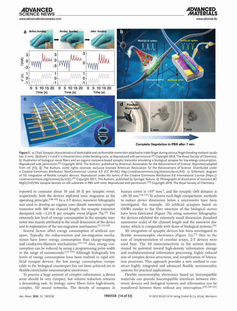
The process of interfacing neuromorphic electronics with elec-tric circuits in computing requires logical operations, because they can be used to model information flow through electrical circuits. Logical operations have been demonstrated using flex-ible 3-T synaptic devices. Boolean logics require two or more inputs, so multiple in-plane gate electrodes have been adopted as presynapses. Multigate structures can emulate the informa-tion processing in a biological neurons in which thousands of inputs from dendrites are integrated and processed for compu-tation and memory-related functions.[175–177] Synaptic integra-tion has an important function for information transformation in the nervous system, and has important implications for neural computation and memory-related functions. Previous synaptic transistors have taken advantage of proton-conducting electrolytes as gate insulators. These electrolytes include graphene oxide (GO),[115] phosphosilicate glass (PSG),[127] and chitosan[57,178] which enable coupling of the electric fields applied by multiple in-plane gate electrodes, to effectively mod-ulate channel conductivity. Here, the protons are regarded as neurotransmitters, and channel conductivity is regarded as the synaptic weight, and in these devices, n-type channel layers were used.
In a device that has two gate electrodes (G1 and G2), at VGS2 = −1.0 V, most of the protons (red dots) in the proton-conducting insulator, i.e., GO (green part) migrate into the insulator/G2 gate electrode interface, so few protons remain in the insulator/channel interface (orange part); as a result, few electrons are electrostatically induced in the channel layer and the drain current (black line in Figure 8b) is not modulated (left panel of Figure 8a). However, at VGS2 = 1.0 V, the electrostatic force drives numerous protons toward the insulator/channel interface (right panel of Figure 8a), so the conductivity of the channel can be easily modulated by adjusting the value of VGS1 (red line in Figure 8b). Thus, the ON state of the drain current was higher than the threshold, and could only be attained when both of the gate inputs were ≥1.0 V. This phenomenon was used to demonstrate “AND” logic operation in flexible synaptic transistors that used GO as proton-conducting gate insulators, IZO as channel layers, and PET as substrates.[115] The input gate voltage of −1.0 V was set as logic “0” and 1.0 V was set as logic “1.” ON current > 0.75 µA could only be achieved when both the input signals of G1 and G2 were “11” (left panel of Figure 8c). In addition, by using different areas of two gate electrodes, that is, larger area of G2′ than G1, the device was applied for “YESG2′” logic in which output EPSC current induced from simultaneous two gate spikes was larger than the threshold (ON state) as long as input G2′ was ≥1.0 V (logic “1”). More specifically, the area of G2′ was designed to be larger than the area of G1, so the EPSC current from G2′ was much higher than from G1. In this case, when the spikes from G1 and G2′ were applied simultaneously, the output EPSC higher than threshold (ON state) could only be dominated by the logic of G2′ (right panel of Figure 8c).
PSG has been used as a proton-conducting gate insu-lator on flexible Si membrane substrates for logic application (Figure 8d).[127] The estimated thickness of the Si membrane was ≈30 µm, which is much smaller than conventional rigid Si
Adv. Mater. 2020, 32, 1903558
© 2019 WILEY-VCH Verlag GmbH & Co. KGaA, Weinheim1903558 (16 of 32)
www.advmat.dewww.advancedsciencenews.com
substrates that are several hundred micrometers thick. Introduc-tion of a modulatory terminal Gm that provides an additional gate input, enabled modulation of the coupling effect among multiple gate inputs, so both the “OR” and “AND” logics were realized in a single device. With a modulatory spike Vm = 0.6 V, the measured EPSC was ≈1.73 µA at presynapse 1 (G1) and ≈1.71 µA at pre-synapse 2 (G2) (left panel of Figure 8e). With synchronous pre-synaptic spikes both at G1 and G2, the EPSC was ≈2 µA. When logic “1” was set as the EPSC value of 1.6 µA, an “OR” logic was demonstrated with Vm = 0.6 V. When Vm of −0.6 V was applied, the EPSC was ≈1.53 µA at G1 and ≈1.47 µA at G2, and with syn-chronous spikes both at G1 and G2, the EPSC was ≈1.78 µA (right panel of Figure 8e), which shows “AND” logic. These results demonstrated that logic operations can be switched between “AND” and “OR” in the same device, by modulating Vm.
A freestanding chitosan membrane prepared by a simple coating–peeling process was used as both a proton-conducting layer and as a flexible substrate (Figure 8f).[57,178] On 100 µm thick freestanding chitosan membrane, multiple in-plane gates were formed as presynaptic input terminals. Here too, “AND” and “OR” logical operations in a single device were realized by controlling the value of Vm.
4.2. Pavlovian Conditioning
Pavlovian conditioning is a learning process in which con-ditioned stimulus (CS; bell ringing) becomes paired with an
unconditioned stimulus (US; sight of food) by repetition of pairing (both bell ringing and sight of food, simultaneously or sequentially).[179] Initially, only the US provokes the uncondi-tioned response (UR; here, salivation). After repeated pairing, the CS alone evokes the conditioned response (CR) of saliva-tion, i.e., the CR can be obtained by learning processes, whereas the UR is a biological response.
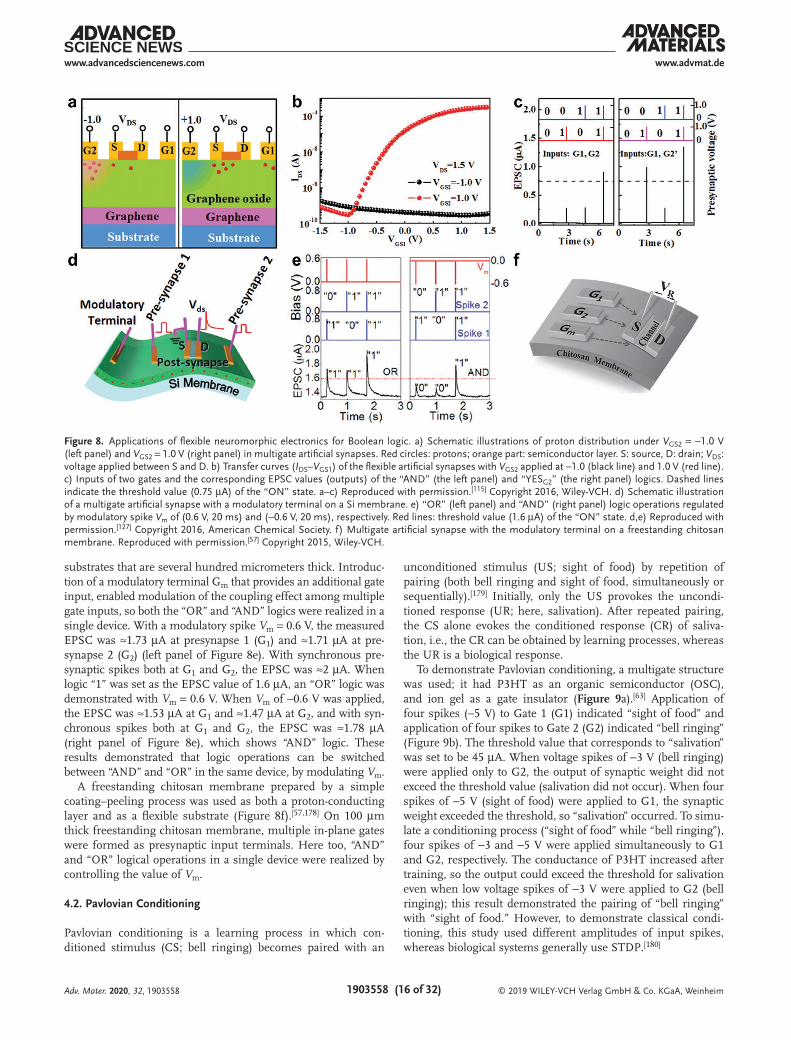
To demonstrate Pavlovian conditioning, a multigate structure was used; it had P3HT as an organic semiconductor (OSC), and ion gel as a gate insulator (Figure 9a).[63] Application of four spikes (−5 V) to Gate 1 (G1) indicated “sight of food” and application of four spikes to Gate 2 (G2) indicated “bell ringing” (Figure 9b). The threshold value that corresponds to “salivation” was set to be 45 µA. When voltage spikes of −3 V (bell ringing) were applied only to G2, the output of synaptic weight did not exceed the threshold value (salivation did not occur). When four spikes of −5 V (sight of food) were applied to G1, the synaptic weight exceeded the threshold, so “salivation” occurred. To simu-late a conditioning process (“sight of food” while “bell ringing”), four spikes of −3 and −5 V were applied simultaneously to G1 and G2, respectively. The conductance of P3HT increased after training, so the output could exceed the threshold for salivation even when low voltage spikes of −3 V were applied to G2 (bell ringing); this result demonstrated the pairing of “bell ringing” with “sight of food.” However, to demonstrate classical condi-tioning, this study used different amplitudes of input spikes, whereas biological systems generally use STDP.[180]
Adv. Mater. 2020, 32, 1903558
Figure 8. Applications of flexible neuromorphic electronics for Boolean logic. a) Schematic illustrations of proton distribution under VGS2 = −1.0 V (left panel) and VGS2 = 1.0 V (right panel) in multigate artificial synapses. Red circles: protons; orange part: semiconductor layer. S: source, D: drain; VDS: voltage applied between S and D. b) Transfer curves (IDS–VGS1) of the flexible artificial synapses with VGS2 applied at −1.0 (black line) and 1.0 V (red line). c) Inputs of two gates and the corresponding EPSC values (outputs) of the “AND” (the left panel) and “YESG2” (the right panel) logics. Dashed lines indicate the threshold value (0.75 µA) of the “ON” state. a–c) Reproduced with permission.[115] Copyright 2016, Wiley-VCH. d) Schematic illustration of a multigate artificial synapse with a modulatory terminal on a Si membrane. e) “OR” (left panel) and “AND” (right panel) logic operations regulated by modulatory spike Vm of (0.6 V, 20 ms) and (−0.6 V, 20 ms), respectively. Red lines: threshold value (1.6 µA) of the “ON” state. d,e) Reproduced with permission.[127] Copyright 2016, American Chemical Society. f) Multigate artificial synapse with the modulatory terminal on a freestanding chitosan membrane. Reproduced with permission.[57] Copyright 2015, Wiley-VCH.
© 2019 WILEY-VCH Verlag GmbH & Co. KGaA, Weinheim1903558 (17 of 32)
www.advmat.dewww.advancedsciencenews.com
Pavlovian learning using STDP was emulated using syn-aptic transistors based on chitosan (Figure 9c).[64] The synaptic weight was changed by controlling the timing between two spikes. The presynaptic spike applied to the gate was consid-ered as “bell ringing” and the postsynaptic spike applied to the drain as “sight of food.” With application of the postsyn-aptic spike (sight of food), the output of synaptic weight was above threshold; this state corresponds to “salivation.” With the presynaptic spike (bell ringing), synaptic weight was below the threshold value (Figure 9d). During the training process, when the presynaptic spike was applied 20 ms before the postsynaptic spike, the synaptic weight was strengthened. After training, application of presynaptic spikes (bell ringing) alone caused the synaptic weight to exceed the threshold (salivation). A detraining process was performed by applying the presynaptic spike 20 ms after the postsynaptic spike, thereby decreasing the synaptic weight. In this case, the application of presynaptic spikes (bell ringing) no longer caused the synaptic weight to exceed the threshold (salivation).
4.3. Pattern and Image Recognition
A neural network is a hierarchical arrangement of neurons joined by synapses that have variable strengths. The strengths
respond in various ways to stimulation; these responses are the basis of learning. An artificial neural network is constructed using artificial synapses with variable conductances to mimic the architecture of a brain, and to achieve its learning ability. Here, we consider the basic artificial neural network (ANN) and the spiking neural network (SNN). The ANNs and the SNNs have revolutionized the fields of machine learning and deep learning. They have realized computer vision such as pattern and image recognition.[181–184] The recognition procedures of neuromorphic electronics consist of learning, memorizing the synaptic weight, and finally recognizing. In this section, the pattern and image recognition processes will be dealt with in two categories of the ANN and the SNN.
4.3.1. Artificial Neural Networks
Learning by ANNs requires vector matrix multiplication (VMM) (Figure 10a).[185] First, input data x are unwrapped to a row vector (1 × n) and each input datum is connected to each value (w; specific weight) of the next layer which is arranged in a matrix for VMM. The weights are modulated by applying training algorithms for forward and backward propagation. During forward propagation, the VMM of ym = Σnwnmxn is
Adv. Mater. 2020, 32, 1903558
Figure 9. Pavlovian conditioning of artificial synapses. a) Schematics of multigated synaptic transistor with P3HT as an organic semiconductor, and ion-gel as a gate insulator. b) Synaptic weight change resulting from presynaptic spikes. Red lines: presynaptic spikes of “bell ringing” (VG2 = −3 V, pulse width tp = 50 ms, pulse period Tp = 50 ms); green lines: “sight of food” (VG1 = −5 V, tp = 50 ms, Tp = 50 ms); blue lines: postsynaptic current showing synaptic weight change. a,b) Reproduced with permission.[63] Copyright 2018, American Chemical Society. c) Schematics of chitosan-based synaptic transistor. d) Synaptic weight change resulted from STDP. Training was realized by setting Δt = −20 ms and detraining was realized by setting Δt = 20 ms. c,d) Reproduced with permission.[64] Copyright 2018, Wiley-VCH.

© 2019 WILEY-VCH Verlag GmbH & Co. KGaA, Weinheim1903558 (18 of 32)
www.advmat.dewww.advancedsciencenews.com
required. When a crossbar array of artificial synapses is used to represent each weight, the VMM can be efficiently calculated by using Kirchhoff’s current law that calculates output current
I G Vm nmn n∑= (4)
where Gnm is the weight (conductance) of the synaptic devices at node (n, m), and Vn is the input voltage of row n.
After forward propagation, synaptic weight is controlled by the backpropagation process, by using a supervised learning method.[186] Error of the jth node is calculated as ej = tj − yj,
where yj is the real output value and tj is the target output. ej is used to guide adjustment of synaptic weight as
w e xij j iα∆ = (5)
where α > 0 is a constant learning rate, ej is the error of jth node, and xi is the ith input. Most of ANNs have two or more layers, so usually i ≥ 2. Artificial synapses must have control-lable multistate conductance (typically >100 states), and have analog conductance for processing a huge amount of informa-tion, like a biological brain. In addition, for ideal operation, the
Adv. Mater. 2020, 32, 1903558
Figure 10. a) Schematic of fully connected ANN. b) Flexible artificial synapses based on PEDOT:PSS. c) Cycle tests of potentiation and depression in PEDOT:PSS-based artificial synapses (10 cycles). b,c) Reproduced with permission.[133] Copyright 2018, American Chemical Society. d) Cycle tests of potentiation and depression of artificial synapses with PEDOT:PSS/PEI film as organic semiconductor layer and Nafion films as gate insulator. Inset: uniform and nonvolatile conductance differences between consecutive stages. Reproduced with permission.[112] Copyright 2017, Springer Nature. e) Conversion of intensity information in each pixel into time-dependent spike forms. f) Schematics of a neuron circuit consisting of inverters (orange), CNT synaptic transistors with floating gate (yellow), and integrators, comparators, and wave form generators (blue). e,f) Reproduced with permis-sion.[92] Copyright 2017, American Chemical Society.
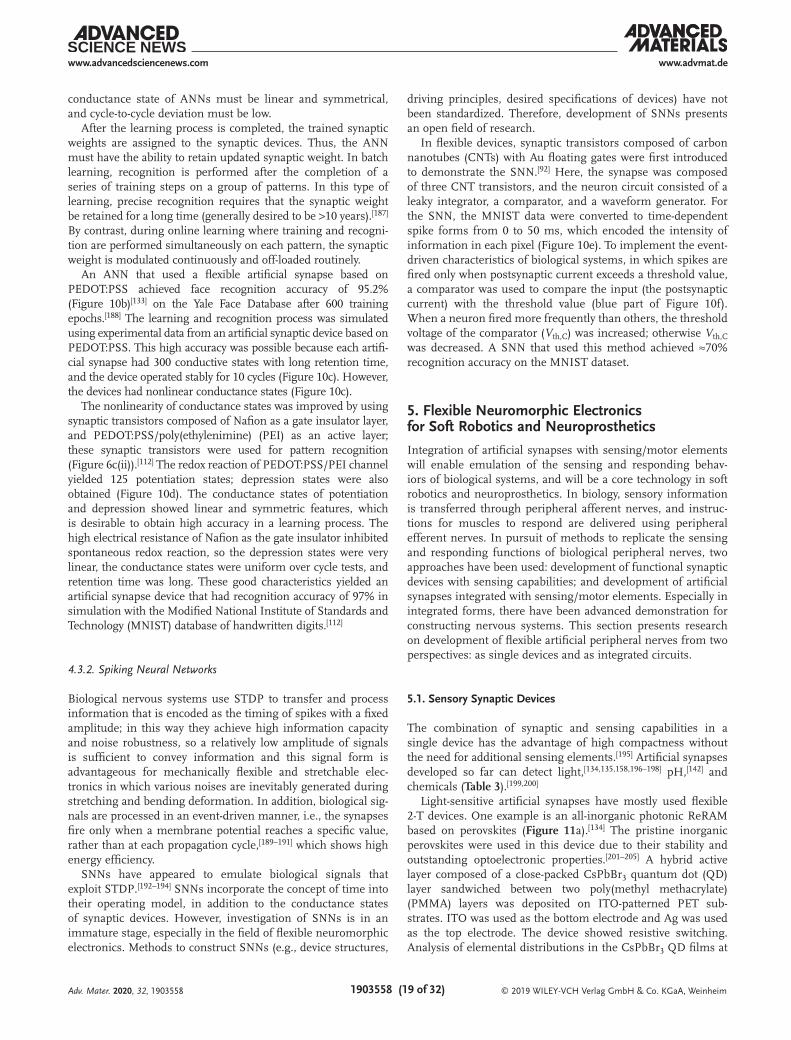
© 2019 WILEY-VCH Verlag GmbH & Co. KGaA, Weinheim1903558 (19 of 32)
www.advmat.dewww.advancedsciencenews.com
conductance state of ANNs must be linear and symmetrical, and cycle-to-cycle deviation must be low.
After the learning process is completed, the trained synaptic weights are assigned to the synaptic devices. Thus, the ANN must have the ability to retain updated synaptic weight. In batch learning, recognition is performed after the completion of a series of training steps on a group of patterns. In this type of learning, precise recognition requires that the synaptic weight be retained for a long time (generally desired to be >10 years).[187] By contrast, during online learning where training and recogni-tion are performed simultaneously on each pattern, the synaptic weight is modulated continuously and off-loaded routinely.
An ANN that used a flexible artificial synapse based on PEDOT:PSS achieved face recognition accuracy of 95.2% (Figure 10b)[133] on the Yale Face Database after 600 training epochs.[188] The learning and recognition process was simulated using experimental data from an artificial synaptic device based on PEDOT:PSS. This high accuracy was possible because each artifi-cial synapse had 300 conductive states with long retention time, and the device operated stably for 10 cycles (Figure 10c). However, the devices had nonlinear conductance states (Figure 10c).
The nonlinearity of conductance states was improved by using synaptic transistors composed of Nafion as a gate insulator layer, and PEDOT:PSS/poly(ethylenimine) (PEI) as an active layer; these synaptic transistors were used for pattern recognition (Figure 6c(ii)).[112] The redox reaction of PEDOT:PSS/PEI channel yielded 125 potentiation states; depression states were also obtained (Figure 10d). The conductance states of potentiation and depression showed linear and symmetric features, which is desirable to obtain high accuracy in a learning process. The high electrical resistance of Nafion as the gate insulator inhibited spontaneous redox reaction, so the depression states were very linear, the conductance states were uniform over cycle tests, and retention time was long. These good characteristics yielded an artificial synapse device that had recognition accuracy of 97% in simulation with the Modified National Institute of Standards and Technology (MNIST) database of handwritten digits.[112]
4.3.2. Spiking Neural Networks
Biological nervous systems use STDP to transfer and process information that is encoded as the timing of spikes with a fixed amplitude; in this way they achieve high information capacity and noise robustness, so a relatively low amplitude of signals is sufficient to convey information and this signal form is advantageous for mechanically flexible and stretchable elec-tronics in which various noises are inevitably generated during stretching and bending deformation. In addition, biological sig-nals are processed in an event-driven manner, i.e., the synapses fire only when a membrane potential reaches a specific value, rather than at each propagation cycle,[189–191] which shows high energy efficiency.
SNNs have appeared to emulate biological signals that exploit STDP.[192–194] SNNs incorporate the concept of time into their operating model, in addition to the conductance states of synaptic devices. However, investigation of SNNs is in an immature stage, especially in the field of flexible neuromorphic electronics. Methods to construct SNNs (e.g., device structures,
driving principles, desired specifications of devices) have not been standardized. Therefore, development of SNNs presents an open field of research.
In flexible devices, synaptic transistors composed of carbon nanotubes (CNTs) with Au floating gates were first introduced to demonstrate the SNN.[92] Here, the synapse was composed of three CNT transistors, and the neuron circuit consisted of a leaky integrator, a comparator, and a waveform generator. For the SNN, the MNIST data were converted to time-dependent spike forms from 0 to 50 ms, which encoded the intensity of information in each pixel (Figure 10e). To implement the event-driven characteristics of biological systems, in which spikes are fired only when postsynaptic current exceeds a threshold value, a comparator was used to compare the input (the postsynaptic current) with the threshold value (blue part of Figure 10f). When a neuron fired more frequently than others, the threshold voltage of the comparator (Vth,C) was increased; otherwise Vth,C was decreased. A SNN that used this method achieved ≈70% recognition accuracy on the MNIST dataset.
5. Flexible Neuromorphic Electronics for Soft Robotics and Neuroprosthetics
Integration of artificial synapses with sensing/motor elements will enable emulation of the sensing and responding behav-iors of biological systems, and will be a core technology in soft robotics and neuroprosthetics. In biology, sensory information is transferred through peripheral afferent nerves, and instruc-tions for muscles to respond are delivered using peripheral efferent nerves. In pursuit of methods to replicate the sensing and responding functions of biological peripheral nerves, two approaches have been used: development of functional synaptic devices with sensing capabilities; and development of artificial synapses integrated with sensing/motor elements. Especially in integrated forms, there have been advanced demonstration for constructing nervous systems. This section presents research on development of flexible artificial peripheral nerves from two perspectives: as single devices and as integrated circuits.
5.1. Sensory Synaptic Devices
The combination of synaptic and sensing capabilities in a single device has the advantage of high compactness without the need for additional sensing elements.[195] Artificial synapses developed so far can detect light,[134,135,158,196–198] pH,[142] and chemicals (Table 3).[199,200]
Light-sensitive artificial synapses have mostly used flexible 2-T devices. One example is an all-inorganic photonic ReRAM based on perovskites (Figure 11a).[134] The pristine inorganic perovskites were used in this device due to their stability and outstanding optoelectronic properties.[201–205] A hybrid active layer composed of a close-packed CsPbBr3 quantum dot (QD) layer sandwiched between two poly(methyl methacrylate) (PMMA) layers was deposited on ITO-patterned PET sub-strates. ITO was used as the bottom electrode and Ag was used as the top electrode. The device showed resistive switching. Analysis of elemental distributions in the CsPbBr3 QD films at
Adv. Mater. 2020, 32, 1903558

© 2019 WILEY-VCH Verlag GmbH & Co. KGaA, Weinheim1903558 (20 of 32)
www.advmat.dewww.advancedsciencenews.com
Adv. Mater. 2020, 32, 1903558
Tabl
e 3.
Sum
mar
y of
flex
ible
neu
rom
orph
ic e
lect
roni
cs w
ith s
ensi
ng fu
nctio
ns.
Stru
ctur
eSe
nsin
g fu
nctio
nM
echa
nism
Mat
eria
lsEn
ergy
[J]/
pow
er [W
] co
nsum
ptio
nPP
F in
dex
(I2/
I 1 ×
100
, Δt)
LTP
(ret
en-
tion
time)
[s]
STD
PSR
DP
Ref
.
Subs
trat
eEl
ectr
odes
(2-
T) G
ate
insu
lato
r (3
-T)
Act
ive
2-T
Che
mic
alIo
n m
igra
tion
PDM
SPE
DO
T:PS
SPE
DO
T:PS
S5.
0 ×
10−9
/5.0
× 1
0−6–
––
–[1
99]
3-T
Che
mic
alC
harg
e tr
appi
ngPV
APV
APC
DTP
Ta)–/
–O
(40
0%, 1
0 s)
––
O[2
00]
2-T
pHIo
n m
igra
tion
PET
ITO
PED
OT:
PSS/
PVA
/
PSSA
b):P
VA/P
EDO
T:PS
S1.
0 ×
10−1
0 /2.
0 ×
10−7
––
––
[136
]
3-T
pHEl
ectr
oche
mic
al
reac
tionc)
PET
n-Si
O2d)
ele
ctro
lyte
IZO
1.56
× 1
0−11 /
1.5
× 10
−9–
––
–[1
42]
2-T
Ligh
tIo
n m
igra
tion
PET
ITO
/Ag
PMM
A/C
sPbB
r 3 Q
Ds/
PMM
A–/
<1.0
× 1
0−4–
4.0
× 10
5–
–[1
34]
2-T
Ligh
tIo
n m
igra
tion
PET
rGO
:(PE
DO
T:PS
S)(C
6H5C
H2C
H2N
H3)
2SnI
42.
925
× 10
−3/5
.85
× 10
−4e)
––
–O
e)[1
35]
2-T
Ligh
tC
harg
e tr
appi
ngPE
TA
uB
lack
pho
spho
rus
9.24
× 1
0−10 /
9.24
× 1
0−9e)
Oe)
(28
5% a
t 280
nm
light
/155
% a
t 365
nm
light
)
75e)
Oe)
Oe)
[198
]
2-T
Ligh
tC
harg
e tr
appi
ng,f)
met
allic
fila
men
tg)
PET
ITO
/Al,
Au,
or
Ag
Silk
:CD
–/≈5
.0 ×
10−3
e)–
––
–[1
58]
2-T
(int
egra
tion)
h)Li
ght
Met
allic
fila
men
tPI
Au/
Ni
Al 2
O3
1.0
× 10
−5/1
.0 ×
10−7
e)–
2.0
× 10
4–
–[2
06]
3-T
(int
egra
tion)
h)Li
ght
Elec
troc
hem
ical
reac
tion,
c)
ferr
oele
ctri
city
PAN
f)P(
VP-
EDM
AEM
AES
)i)/
P(V
DF-
TrFE
)
PIID
-BTj)
7.5
× 10
−11 /
–O
(20
0%, 2
0 m
s)1.
63 ×
104
–O
[132
]
2-T
(int
egra
tion)
h)Pr
essu
reIo
n m
igra
tion
PET
ITO
/Ag
CιC
8.0
× 10
−8/8
.0 ×
10−7
––
––
[78]
3-T
(int
egra
tion)
h)Pr
essu
reEl
ectr
oche
mic
al
reac
tionc)
PIC
hito
san
PDPP
3T1.
25 ×
10−8
/2.5
× 1
0−7O
(19
0%, 1
00 m
s)25
–O
[171
]
3-T
(int
egra
tion)
h)St
rain
Elec
troc
hem
ical
reac
tionc)
PET
Ion
gel e
lect
roly
teG
raph
ene
1.5
× 10
−9/1
.5 ×
10−8
k)O
k) (
140%
, 300
ms)
3.24
k)–
Ok)
[207
]
a)Po
ly[4
-(4,
4-di
hexa
decy
l-4H
-cyc
lope
nta-
[1,2
-b:5
,4-b
′]dith
ioph
en-2
-yl)
-alt-
[1,2
,5]th
iadi
azol
o[3,
4-c]
pyri
dine
]; b)
Poly
(sty
rene
sul
foni
c ac
id);
c)El
ectr
oche
mic
al r
eact
ion
occu
rs w
ith i
on m
igra
tion;
d)N
anog
ranu
lar
SiO
2; e)
This
was
ob
tain
ed w
ith l
ight
pul
ses
(not
ele
ctri
cal
puls
es);
f)D
evic
es w
ith A
l an
d A
u an
odes
exh
ibite
d w
rite
-onc
e re
ad-m
any-
times
mem
ory
beha
vior
s du
e to
the
ir c
harg
e-tr
appi
ng m
echa
nism
; g)
Met
allic
fila
men
t w
as t
he m
ain
mec
hani
sm f
or r
esis
tive
tran
sitio
ns o
f A
g an
ode–
base
d de
vice
s; h)
Syna
ptic
dev
ices
wer
e in
tegr
ated
with
sen
sors
; i)Po
ly[(
1-vi
nylp
yrro
lidon
e)-c
o-(2
-eth
yldi
met
hyla
mm
onio
ethy
l met
hacr
ylat
e et
hyl s
ulfa
te)]
; j)Po
ly(i
soin
digo
-co-
bith
ioph
ene)
; k)O
btai
ned
from
str
ain
stim
uli (
not
elec
tric
al p
ulse
s).

© 2019 WILEY-VCH Verlag GmbH & Co. KGaA, Weinheim1903558 (21 of 32)
www.advmat.dewww.advancedsciencenews.com
LRS determined that the resistive switching effect was a result of formation and annihilation of metallic filaments and Br− ion vacancies driven by the external electric field. This phenom-enon was evoked by a combination of applied electric field and light illumination, i.e., illumination increased the ON/OFF ratio, and yielded multilevel data storage in the devices (Figure 11b). The devices were combined to form an “OR” logic gate that used light and electric field as the input signals. How-ever, the toxicity of lead in lead halide perovskites is a major obstacle to real-world applications.
Lead-free 2D perovskite (PEA)2SnI4 has been in a flexible light-stimulated synaptic device (Figure 11c).[135] By using hybrid films of rGO and PEDOT:PSS as flexible transparent electrodes on PET substrates, the devices maintained their initial memory characteristics after 1500 cycles of bending, which is much better mechanical flexibility and durability than
otherwise-identical flexible devices that had a Au electrode. Light illumination induced formation of electron–hole pairs, and some of electrons were trapped in Sn vacancies. When the light was turned off, the photocurrent decreased slowly with a relatively long relaxation time (≈3.6 s); the slow decay was a result of slow release of electrons trapped in the vacan-cies. Under a second exposure of light, the trapped electrons in the Sn vacancies facilitated increase in the number of pho-toinduced holes. When illuminated at various light intensities, a device that used this mechanism showed synaptic behaviors such as SDDP, SRDP, SNDP, and EPSC (Figure 11d,e).
Biomaterials have also been used in photosensitive synaptic devices. These devices were biodegradable and biocompatible, so they enable biocompatible interfaces between electronic devices and biological objects. These traits enable biotechnological and medicinal applications of artificial synapses as implantable
Adv. Mater. 2020, 32, 1903558
Figure 11. Photosensitive artificial synapses based on two-terminal structures. a) Schematic and b) I–V characteristics of the CsPbBr3-QD-based ReRAM devices in the dark or under UV illumination (peak wavelength 365 nm; intensities 0.041 ≤ IL ≤ 0.153 mW cm−2). a,b) Reproduced with per-mission.[134] Copyright 2018, Wiley-VCH. c) Schematic diagram, d) ΔEPSC under light pulse (peak wavelength 470 nm; intensity 40 µW cm−2) with various pulse durations 1 ≤ tduration ≤ 200 ms, and e) ΔEPSC under light pulses (tduration = 10 ms) at 3.4 ≤ IL ≤ 39.2 µW cm−2 of 2D (PEA)2SnI4 flexible photoconductors. c–e) Reproduced with permission.[135] Copyright 2018, The Royal Society of Chemistry. f) Cross-sectional scanning electron micro-scopy image of the CDs–silk based ReRAM. g–i) I–V characteristics based on metal anode of Al (g), Au (h), and Ag (i) under UV light exposure (peak wavelength 365 nm; 0 ≤ IL ≤ 0.15 mW cm−2. f–i) Reproduced with permission.[158] Copyright 2018, Wiley-VCH.

© 2019 WILEY-VCH Verlag GmbH & Co. KGaA, Weinheim1903558 (22 of 32)
www.advmat.dewww.advancedsciencenews.com
electronic devices, biosensors, and wearable systems. A photo-sensitive ReRAM based on metal anode/carbon dots (CDs)–silk protein/ITO was systematically investigated with Al, Au, or Ag as an anode (Figure 11f).[158] Devices with Al and Au anodes exhibited write-once read-many-times memory behaviors as a consequence of their charge-trapping mechanism (Figure 11g,h). By contrast, electrochemical metallization occurred as a result of reversible bipolar-resistive switching properties of the Ag-based devices (Figure 11i). Use of CDs that have light-tunable charge-trapping capacity, yielded a set voltage and ON current that could be effectively tuned by exposure to ultraviolet light.
A pH-sensing synaptic device was demonstrated using a flex-ible IZO-based synaptic transistor with multiple input gates (Figure 12a).[142] A nanogranular SiO2 (n-SiO2) electrolyte film was deposited as a proton-conducting gate insulator on an ITO-coated PET substrate. A Ag/AgCl reference electrode immersed in a solution droplet acted as the sensing gate (G1) and in-plane
Al electrodes were used as the control gates (G2). As previ-ously (Section 4.1), the carrier density of the IZO channel was modulated by the effective electric field that was coupled by G1 and G2. The flexible synaptic transistors endured more than 1000 flexing-and-flattening cycles with negligible change in their transfer characteristics. Acidic solutions increased the positive surface potential at the solution/SiO2 interface, and the positive surface potential drove protons in the SiO2 electrolyte toward the SiO2/IZO interface. This process induces additional electrons in the IZO channel, so as pH decreased, the magnitude of EPSC increased (Figure 12b). Control of the voltage of G1, especially with an appropriate negative bias, increased the devices’ sensitivity and reduced their energy consumption.
A chemical-sensing synaptic device based on whole organic materials was demonstrated to detect dopamine (DA) without the need for a specific recognition moiety. The artifi-cial synapse consisted of two electrodes of PEDOT:PSS, and
Adv. Mater. 2020, 32, 1903558
Figure 12. a) Structure and b) pH-sensing performances based on a single spike mode of pH-sensing artificial synapses. a,b) Reproduced under the terms of the Creative Commons Attribution 4.0 International License (https://creativecommons.org/licenses/by/4.0/).[142] Copyright 2015, Springer Nature. c) Dose curves in response to DA solutions (black squares), DA + 100 × 10−6 m AA (green hexagons), and DA + 3 × 10⁻⁶ m UA (purple lozenges) of chemical (dopamine)-sensing artificial synapses. S is defined as ratio of variation in relaxation time. Reproduced with permission.[199] Copyright 2017, American Chemical Society. d) Schematic diagram of human olfactory receptors and organs, e) output signals, and f) various synaptic characteristics (LTP and PPF) of chemical-sensing artificial synapses in response to 20 ppm NO2 gas pulses. d–f) Reproduced with permission.[200] Copyright 2019, The Royal Society of Chemistry.

© 2019 WILEY-VCH Verlag GmbH & Co. KGaA, Weinheim1903558 (23 of 32)
www.advmat.dewww.advancedsciencenews.com
flexible substrates of PDMS.[199] The devices may sense DA by responding to attractive and repulsive forces between the analytes and PEDOT:PSS. That is, since DA is a cation at physiological pH and PSS is a cation-exchange polymer, so attractive forces would form between them. Both ascorbic acid (AA) and uric acid (UA) are anions at physiological conditions, so they develop electrostatic repulsion with PSS. This mecha-nism enabled the synaptic device to selectively detect DA con-centrations [DA] as low as 1 × 10⁻¹² m even in the presence of [AA] = 100 × 10−6 m and [UA] = 3 × 10⁻⁶ m which are physi-ological levels of two major interfering agents in cerebrospinal fluid and the striatum (Figure 12c).
A human olfactory system was emulated by a conform-able 3-T synaptic device for sensing hazardous gas (NO2) (Figure 12d).[200] This NO2-sensing synaptic device was fabricated on a freestanding polyvinyl alcohol (PVA) substrate (Figure 12e). When the device was exposed to pulses of NO2 gas, the NO2 molecules were captured and remained on the surface of the semiconductor layer, which acted as electron trapping sites. This process led to increased accumulation of holes in the semiconductor layer, and as a consequence, the current increased. When the gas pulse ceased, the increased current was maintained to some extent, because the captured gas molecules in the semiconductor layer took some time to be dedoped from it. Thus, this NO2-sensing artificial synapse exhibited synaptic properties.
5.2. Artificial Synapses Integrated with Sensors
To use external stimuli as inputs of artificial synapses, they can be integrated with various sensors such as photo- and pressure sensors. These kinds of integrated circuits have been composed of various device components, exploited different mechanisms, and shown various synaptic characteristics (Table 3).
To emulate human visual-perception systems, a memristor was integrated with a UV image sensor on flexible PI sub-strates in series (Figure 13a).[206] In the artificial visual memory system, Al2O3 was used as active layers of the memristors due to its good bipolar resistive switching properties, and in the image sensors, In2O3 was used as active layers because of its high sensitivity to UV light. In the integrated system, the detec-tion of UV light by the image sensors was recorded in mem-ristors, and this realized detection and memory capacities that provide and advance to emulation of human visual memory. Visual memory arrays composed of 10 × 10 pixels detected a butterfly shaped image and stored it for at least 1 week (top panel of Figure 13b). The stored information could be erased by a reset-negative voltage and reproduced repeatedly; this result demonstrated the reusability of the integrated devices (bottom panel of Figure 13b).
Another approach used a ferroelectric/electrochemical mod-ulated organic synaptic device that was integrated with organic light-sensitive element (Figure 13c).[132] In previous studies,
Adv. Mater. 2020, 32, 1903558
Figure 13. Flexible artificial synapses integrated with photosensitive elements. a) Schematic diagram of an artificial visual memory system by the integration of a memristor and a UV image sensor and b) information storage characteristics for the applied patterned light and reusability of the arrays of these systems. a,b) Reproduced with permission.[206] Copyright 2018, Wiley-VCH. c) Schematic of a LOND (ferroelectric/electrochemical modulated organic synaptic device integrated with an organic light-sensitive element) and d) response characteristics of LONDs under different wavelength of light (top panel: 850 nm; bottom panel, 550 nm). c,d) Reproduced with permission.[132] Copyright 2018, Wiley-VCH.

© 2019 WILEY-VCH Verlag GmbH & Co. KGaA, Weinheim1903558 (24 of 32)
www.advmat.dewww.advancedsciencenews.com
Adv. Mater. 2020, 32, 1903558
LTP functions that are related with information consolidation and memory were unreliable. In this research, to strengthen the nonvolatile memory functions, a ferroelectric organic material (P(VDF-TrFE)) was additionally inserted as a gate insu-lator layer in the synaptic transistors. This device is advanta-geous over conventional electrochemical transistors, because the extra ferroelectric LTP provides reliable nonvolatile memory and exhibits three types of plasticity: STP and LTP by electro-chemical doping and dedoping, and ferroelectric LTP by dipole switching. By using the artificial synapses as information pro-cessing units, a light-triggered organic neuromorphic device (LOND) was demonstrated. The LOND transduced light inten-sity and frequency information into synaptic signals either in volatile or nonvolatile forms. It could also recognize colors: the volatility of synaptic signals was different at light wavelength, i.e., electrochemical LTP at 850 nm and ferroelectric LTP at 550 nm (Figure 13d).
Artificial strain and touch perception has been demon-strated by integrating artificial synapses with nanogenerators (NGs).[81,207] In Figure 14a, a memristor was integrated with the self-powered NG.[81] The NG converts wasted mechanical energy (pressure information) to electrical signals (voltage pulses) which drive the artificial synapses. The sensing parts in this system were self-powered, so only the synaptic components dis-sipated energy; this attribute was distinct from the systems that have been described so far, which required additional energy to operate the sensing elements. In addition, biocompatible devices composed of amorphous NKN films grown on TiN/PI substrates were used both in the memristors and the NGs. The
system showed various synaptic characteristics such as STP/LTP transition, SRDP, and metaplasticity.
For the construction of a pressure sensory alarm system, a flexible artificial nociceptor was connected with a piezoresis-tive pressure sensor (Figure 14b).[78] A nociceptor is a general receptor that signals a stimulus is harmful, so nociceptors would be useful in robots and prosthetics to help them to avoid injury in dangerous environments. Here, the artificial nocic-eptors were based on flexible Ag/CιC/ITO/PET memristors, because the biopolymer is abundant, inexpensive, biocom-patible, and mechanically flexible. The biological nociceptive characteristics of threshold, relaxation, allodynia, and hyper-algesia behaviors were emulated by formation and rupture of Ag filaments in the memristors. When the applied voltage (VA) was lower than the threshold voltage of the memristor (Vth,M), its resistance is much higher than the series resistor in Ch2, so full voltage drop occurred at the memristor. How-ever, when VA > Vth,M, the memristor was turned ON and the voltage dropped by nearly half at the series resistor. Specifically, with the application of low pressure (black curves), VA < Vth,M was generated from a piezoelectric module (the top panel of Figure 14c) so that no output alarm signal (Ch2) was generated (bottom panel of Figure 14c). Under medium pressure (blue curves), when VA approached Vth,M = 0.6 V, an alarm signal was generated. Finally, when high pressure (red curves) was applied, higher alarm signal was produced at a shorter onset time. These nociceptors had the valuable characteristic of becoming sensitized: when a second pressure lower than the threshold value was applied, the alarm signal was generated
Figure 14. Flexible artificial synapses integrated with tactile sensors. a) A memristor integrated with a self-powered NG. Reproduced under the terms of the Creative Commons Attribution 4.0 International License (https://creativecommons.org/licenses/by/4.0/).[81] Copyright 2017, The Authors, published by Springer Nature. b) Schematic diagram of a pressure sensory alarm system with a flexible artificial nociceptor (memristor) and a piezoresistive pressure sensor. c) Voltage at the piezoelectric module Ch1 (top panel) and voltage applied at the series resistor Ch2 (bottom panel). b,c) Reproduced with permission.[78] Copyright 2019, The Royal Society of Chemistry. d) Schematic (top panel) and equivalent electrical circuit (bottom panel) of the DOT-TPS (a synaptic transistor integrated with a transistor-type pressure sensor) and e) its responses with increasing touch times (the top panel) and various repetition cycles (the bottom panel). d,e) Reproduced with permission.[171] Copyright 2017, Wiley-VCH.

© 2019 WILEY-VCH Verlag GmbH & Co. KGaA, Weinheim1903558 (25 of 32)
www.advmat.dewww.advancedsciencenews.com
Adv. Mater. 2020, 32, 1903558
with no delay time. This trait can accelerate a prosthetic’s avoid-ance of damaging stimuli.
A dual organic transistor–based tactile perception element (DOT-TPE) was demonstrated by integrating a synaptic tran-sistor with a transistor-type pressure sensor. The DOT-TPE per-mits immediate sensing of pressure stimuli and synapse-like information processing in a single element (Figure 14d).[171] Polymers were used to achieve organic synaptic transistors: poly(diketopyrrolopyrrole-terthiophene) (PDPP3T) was used as an OSC, and chitosan was used as a proton-conducting gate insulator. A DOT-TPE is an integrated synaptic transistor, so the output of the DOT-TPE is determined by a combination of the intensity, frequency, duration, and the number of pressures (Figure 14e). This characteristic is distinct from a stand-alone sensing device, in which the output current is governed only by the pressure intensity, regardless of other information about the applied pressure. However, although this integrated system could distinguish tactile patterns, it could not learn to identify and recognize them.
5.3. Integration for Constructing Artificial Nervous Systems
The previously mentioned sensory synaptic devices and inte-grated circuits could sense external stimuli and showed various synaptic characteristics, when sensory information was provided as input. However, the postsynaptic output signals from artificial synapses has not been used to demonstrate practical functions for advanced applications such as recogni-tion/learning and motor functions; this section introduces inte-grated systems for constructing artificial nervous systems that perform advanced functions (Table 4).
5.3.1. Recognition and Learning
A neuromorphic tactile processing (NeuTap) system that uses machine learning was introduced to provide learning capability to emulate the cognitive functions of animals.[208] The system consisted of a resistive pressure sensor, a soft ionic cable, and a synaptic transistor, to respectively emulate a receptor, an axon, and a synapse in a biological sensory neuron (Figure 15a). Tactile stimuli were converted into electrical signals by the pres-sure sensor, then transmitted through the ionic cable to the synaptic transistor for information processing. To integrate and differentiate the spatiotemporal features of tactile patterns, two pressure-sensing terminals were combined with the synaptic transistor; depending on the pressure loads on the two sensors, the applied voltages generated by each sensor were coupled through the PVA-based gate insulator of the synaptic transistor, and thereby modulated the conductivity of the indium tung-sten oxide (IWO) channel (Figure 15b). As a proof-of-concept, one sensing terminal in the NeuTap system was used for tac-tile pattern recognition, and the machine-learning method was implemented on the system (Figure 15c). Convex patterns were defined as “1” and flat patterns were defined as “0”. Pattern pairs were labeled using binary codes of “00,” “01,” “10,” and “11.” The error rate of recognition decreased from 44% to 0.4% after repeated training; this result is similar to the perceptual learning processes of the humans.
An artificial haptic neuron system was constructed by com-bining a 2-T piezoresistive pressure sensor with a Nafion-based organic memristor (Figure 15d).[209] This system learned to rec-ognize English letters under a supervised learning method. The pressure sensor transformed pressure stimuli into electrical signals. The Nafion-based memristor exhibited fundamental
Table 4. Summary of flexible neuromorphic electronics for artificial nervous systems (ANSs).
Ref. Structurea) Sensing input/pulse conversion
Energy consump-tion of systemsb)
Functions Signal recognitionc)
Biocompatibility of signalsd)
Similarity with biologye)
Publication date
[109] 3-T Light/no Lowf) Sensorimotor nervous system
(artificial motor nerves) and
recognition (Morse code of
English letters)
Optical signal
recognition (26
Morse codes of
English letters)
No, possible
biointerfacing
High November
2018
[110] 3-T Pressure/yes Relatively lowg) Reflex arc in PNS (artificial
sensory and biological motor
nerves) and recognition
(Braille characters, object
movement)
Improved
recognition in
ANSh) (4 Braille
characters)
Yes High June 2018
[208] 3-T Pressure/no Highi) Recognition and learning
(two-bit binary code)
KNN (3 pat-
terns) (error rate
0.4%)
No biointerface Low July 2018
[209] 2-T Pressure/no Highi) Recognition and learning
(English characters)
KNN (6 English
characters)
(accuracy 91.7%)
No biointerface Low May 2019
a)Structure of artificial synapses; b)Energy consumption to construct whole nervous systems and demonstrating their functions; c)Signal recognition ability of the systems; d)Output signals of neuromorphic electronics were compatible with biological counterparts, so they can be applied to neuroprosthetics; e)Operating principles and functions of the integrated systems were similar to those in biology; f)This system used self-powered sensor elements (photovolatics) as sensing parts. Usually, sensing parts consume higher energy compared to artificial synapses; g)This system demonstrated its functions (recognition and hybrid reflex arc) itself (without aid of learning methods); h)To emulate signal integration and partial information processing in biological synapses, additional artificial synapses were connected to several sets of two pixels for Braille reading (one pixel is composed of one pressure sensor and one ring oscillator), so it improved the discrimination among the Braille characters; i)Refs. [208] and [209] adopted learning methods for demonstrating advanced functions (learning), so high energy consumption was inevitable.

© 2019 WILEY-VCH Verlag GmbH & Co. KGaA, Weinheim1903558 (26 of 32)
www.advmat.dewww.advancedsciencenews.com
Adv. Mater. 2020, 32, 1903558
synaptic functions such as PPF, PPD, and STDP with low power consumption of 10–200 pJ per synaptic event, and high stability for >104 cycle tests. The combination of the pressure sensor and the memristor could process and learn various tactile patterns, by comparing the amplitude, duration, frequency, and speed of external pressure. English characters have dif-ferent numbers and durations of strokes; this individuality was exploited for this integrated system to recognize English let-ters (Figure 15e). A supervised learning method that used the k-nearest neighbors (KNN) algorithm was implemented on the system. After training, the classification accuracy for each letter reached 91.7%; this result demonstrated successful perceptual learning (Figure 15f).
5.3.2. Artificial Peripheral Nervous Systems
To demonstrate a hybrid reflex arc that was composed of arti-ficial sensory nerves and biological motor nerves, the artificial sensory nerve was made of pressure sensors, an organic ring oscillator, and a synaptic transistor (Figure 16a).[110] Currently available neuromorphic devices emulate biological systems only partially. The devices and systems that have been demon-strated so far use only spike-based external stimuli, although numerous other forms of stimuli are encountered in the real world. Biological systems use signal spikes when transmitting and processing information; therefore, to achieve biocompat-ibility of signal form, a spike-encoding method is required, especially for prosthetics. For this purpose, ring oscillators
have been introduced in a bioinspired artificial mechanosen-sory nerve to convert external stimuli to biocompatible spike signals. The system emulated information processing and other functions of biological systems. In the artificial nervous systems, an artificial mechanoreceptor (a pressure sensor) was integrated with an artificial nerve fiber (a ring oscillator) which converts pressure information to action potentials (spike-form voltage). The spike-form voltages from many arti-ficial nerve fibers were connected to a synaptic transistor that processed the information. The synaptic transistor was inter-faced with biological motor nerves in a detached insect leg (Figure 16b). This combination of an artificial sensory nerve and a biological motor nerve constituted a hybrid reflex arc; it actuated the insect’s muscles in response to external pressure information (Figure 16c). This device verifies the applicability of artificial sensory nerves for neuroprosthetics. The artificial afferent nerves also successfully detected movement direction of objects and identified Braille characters. To identify Braille characters, each synaptic device was connected to each pixel (one pressure sensor and one ring oscillator). Then, additional 11 synaptic devices were connected to 11 sets of two pixels, which emulated the function of signal integration of biological counterparts. Through this signal integration, Braille letters were more distinguishable. This provided a new approach for improving perception accuracy without the aid of a learning method which was adopted in previously reported recognition studies (Section 5.3.1).[208,209]
In addition, sensorimotor nervous systems were also dem-onstrated (Figure 17a).[109] To achieve these nervous systems,
Figure 15. Flexible artificial tactile-sensitive nervous systems with learning capability. a) Comparison of a NeuTap system with a biological sensory neuron. b) Current responses of the NeuTap neuron with two pressure sensors when sensor 1 and sensor 2 are pressed individually (cases I and II) and when both the sensors are pressed simultaneously (case III) (VDD1 = VDD2 = −1.0 V). c) Schematic of tactile pattern recognition and perceptual learning by the NeuTap equipped with the machine learning method. a–c) Reproduced with permission.[208] Copyright 2018, Wiley-VCH. d) An artificial haptic perception system consisting of a pressure sensor (i) and a Nafion-based memristor (ii). e) Recognition of English characters and f) perceptual learning processes with the implementation of supervised learning method (KNN algorithm) on the system. d–f) Reproduced with permission.[209] Copyright 2019, Wiley-VCH.

© 2019 WILEY-VCH Verlag GmbH & Co. KGaA, Weinheim1903558 (27 of 32)
www.advmat.dewww.advancedsciencenews.com
Adv. Mater. 2020, 32, 1903558
artificial synapses can induce contraction of artificial mus-cles by transferring an action potential in the same way that human motor nerves operate. Then, artificial motor nerves can be applied to achieve biomimetic natural movement by con-necting biological nerves in bioinspired soft robots and neural prostheses. In addition, flexible and stretchable artificial nerves that maintain electrical properties even while bent or stretched can be applied to soft robots and neural prostheses that undergo movements such as bending, folding, twisting, and stretching. To fabricate flexible and stretchable artificial synapses, electro-spun nanowires that had low mechanical modulus and excel-lent flexibility were transferred to a prestretched substrate; they buckled when the prestrain of the substrate was released (Figure 17b).[109,146,147] Parallel and perpendicular stretching of the substrate caused stretching or folding of buckled nanowires, but they maintained morphological and electrical properties without significant plastic deformation (Figure 17c).[109,146,147] Ion-gel and CNT S/D electrodes also conformed to substrate deformation without breakdown. An ion gel–gated stretch-able synaptic transistor based on organic nanowires did not show noticeable degradation in electrical properties even when it was stretched 100% in the parallel or perpendicular direc-tions (Figure 17c).[109] When various patterns of presynaptic voltage pulses were applied, the devices exhibited stable syn-aptic plasticity regardless of strain (Figure 17d,e).[109] A stretch-able artificial synaptic transistor has been used to implement artificial sensorimotor nerves that control artificial muscles (Figure 17a).[109] Artificial sensorimotor nerves were composed of a photodetector that emulates light receptors, a stretchable organic nanowire artificial synapse, and a polymer actuator that mimics biological muscle fiber.[109] The artificial syn-apse stimulated the artificial muscle fiber by receiving artifi-cial action potentials from an artificial light receptor.[109] By controlling the contraction of the artificial muscle fiber with
the firing frequency of artificial action potentials, the artificial sensorimotor nerve emulated contraction of a biological muscle in response to the signal from a neuromuscular junction.[109] Depending on the firing frequency of the action potential, con-traction of a biological muscles changes from a twitch (weak and short forces), to a summation of twitches, and to tetanus (strong contraction).[109] In the artificial nerves, the displace-ment of the polymer actuator was controlled by the firing of the artificial action potential (Figure 17f).[109] Artificial synapses that control biological and artificial motor units can advance the development of next-generation biomedical electronics, bioin-spired soft robots, and neural prostheses.
6. Conclusion
We have reviewed the progress in development of flexible neu-romorphic electronics, at the single-device and system levels. We have described basic background including device struc-tures, working mechanisms, synaptic plasticity, and main parameters of flexible artificial synapses compared with those of biological synapses. Flexible artificial synapses use various working mechanisms (metallic filament, charge trapping, phase change, ferroelectricity, ion migration, electrochemical reaction), various geometries (2-T, 3-T, battery-like, multigated) and materials (OSCs, inorganic oxide semiconductors, perov-skite, carbon-based nanomaterials, transition metal dichalco-genide nanomaterials), and multipixel arrays. By emulation of brain functions such as logic operation, associative learning, and pattern and image recognition, flexible artificial synapses have proven their potential for use in advanced AI and cogni-tive computing.
Flexible neuromorphic electronics that have artificial sensory synapses (sensing of pH, light, and chemicals) and integrated
Figure 16. a) Comparison of biological mechanoreceptor nerves and an artificial sensory nerve made of pressure sensors, an organic ring oscillator, and a synaptic transistor. b) Hybrid reflex arc by integration of the artificial sensory nerve with a biological motor nerve and c) force of leg extension in response to pressure on the artificial afferent nerve in (b). Pressure: 39.8 kPa; duration: 0.5 s. a–c) Reproduced with permission.[110] Copyright 2018, American Association for the Advancement of Science.

© 2019 WILEY-VCH Verlag GmbH & Co. KGaA, Weinheim1903558 (28 of 32)
www.advmat.dewww.advancedsciencenews.com
Adv. Mater. 2020, 32, 1903558
systems with external sensory elements (touch, light, sound) have the potential to be applied in next-generation wearable electronics, soft robotics, and neuroprosthetics. Neuroinspired robotic technology that operates the robot’s sensory/motor units by transmitting signals in a mechanism similar to those of biological nervous systems can be used in human-like soft robots. Furthermore, neuromorphic electronics can help to replace damaged nerves or can be used in neuroscience as a tool to study sensory and motor neuronal disorders.
For realization, mechanical compliance of artificial synapses and nerves is important for the form factor of future biocom-patible neuromorphic electronics. Thus, the devices must be tolerant of the mechanical deformation. However, system-atic research about change of synaptic properties resulting from mechanical stress is still lacking, despite the recent large amount of research on flexible artificial synapses. Par-ticularly, device structures and materials must be optimized to achieve stable synaptic responses based on short-term or long-term synaptic potentiation or depression regardless of
mechanical strain. Furthermore, applications of stretchable and biocompatible artificial synapses will expand to include skin-attachable and implantable neuromorphic electronics for wearable computing, health monitoring, and sensorimotor neural signal transmission; forms may include prosthetics, exoskeletons, and cybernetic devices. For example, artificial sensory synapses use input/output signals similar to electrical biosignals (e.g., electroencephalogram, electrocardiogram, elec-tromyogram, and electrooculography), so the artificial synapses can be applied to bionic electronic devices that monitor body signals and exchange sensory or motor signals by connecting them with human nerves for medical care, rehabilitation, mili-tary (e.g., exoskeleton), and aerospace (e.g., advanced space suit) purposes. For this purpose, the development of sensors that are highly sensitive to external stimuli (e.g., pH, chemicals, light, touch, sound) as well as to biosignals, and the precise matching of amplitude and rate of electrical signals between biology and electronics will be important. Researchers already have many approaches to demonstrate stretchable, implantable,
Figure 17. Sensorimotor synaptic system. a) Schematic of an artificial sensorimotor nerve composed of a photodetector (light receptor), a stretchable organic nanowire synaptic transistor (synapse), and a polymer actuator (biological muscle fiber). b) Morphology change of a buckled organic nanowire with and without 100% strain. c) Electrical characteristics of a stretchable organic nanowire synaptic transistor at 0, 50, and 100% strains. d) Spike-voltage-dependent plasticity (−0.3 to −1 V) and e) light-triggered spike-number-dependent plasticity (1–50 spikes) of a stretched artificial synapse from 0% to 100% strains. f) Photographs of polymer actuator controlled by artificial sensorimotor nerve. a–f) Reproduced with permission.[109] Copyright 2018, The Authors, published by American Association for the Advancement of Science. Reprinted/adapted from ref. [109]. © The Authors, some rights reserved; exclusive licensee American Association for the Advancement of Science. Distributed under a Creative Commons Attribution NonCommercial License 4.0 (CC BY-NC) http://creativecommons.org/licenses/by-nc/4.0/.

© 2019 WILEY-VCH Verlag GmbH & Co. KGaA, Weinheim1903558 (29 of 32)
www.advmat.dewww.advancedsciencenews.com
Adv. Mater. 2020, 32, 1903558
and even self-healable electronic devices, so advanced biocom-patible neuromorphic electronic devices are expected to appear soon, and will revolutionize the future of computing, robotics, and neuroscience.
AcknowledgementsH.-L.P. and Y.L. contributed equally to this work. This work was supported by the Center for Advanced Soft-Electronics funded by the Ministry of Science and ICT as Global Frontier Project (Grant No. 2013M3A6A5073175). This work was also supported by the Creative-Pioneering Researchers Program through Seoul National University (SNU) and the National Research Foundation of Korea (NRF) grant funded by the Korea government (Ministry of Science and ICT) (Grant No. NRF-2016R1A3B1908431).
Conflict of InterestThe authors declare no conflict of interest.
Keywordsartificial nerves, artificial synapses, flexible electronics, neuromorphic electronics
Received: June 4, 2019Revised: July 10, 2019
Published online: September 26, 2019
[1] M. Hu, C. E. Graves, C. Li, Y. Li, N. Ge, E. Montgomery, N. Davila, H. Jiang, R. S. Williams, J. J. Yang, Q. Xia, J. P. Strachan, Adv. Mater. 2018, 30, 1705914.
[2] S. Furber, J. Neural Eng. 2016, 13, 051001.[3] Y. van de Burgt, A. Melianas, S. T. Keene, G. Malliaras, A. Salleo,
Nat. Electron. 2018, 1, 386.[4] N. Raeis-Hosseini, Y. Park, J. S. Lee, Adv. Funct. Mater. 2018, 28,
1800553.[5] D. Sarkar, J. Tao, W. Wang, Q. Lin, M. Yeung, C. Ren, R. Kapadia,
ACS Nano 2018, 12, 1656.[6] M. A. Zidan, J. P. Strachan, W. D. Lu, Nat. Electron. 2018,
1, 22.[7] P. Gkoupidenis, N. Schaefer, B. Garlan, G. G. Malliaras, Adv.
Mater. 2015, 27, 7176.[8] G. Voglis, N. Tavernarakis, EMBO Rep. 2006, 7, 1104.[9] Y. Lee, T. W. Lee, Acc. Chem. Res. 2019, 52, 964.
[10] W. Jayathilaka, K. Qi, Y. Qin, A. Chinnappan, W. Serrano-Garcia, C. Baskar, H. Wang, J. He, S. Cui, S. W. Thomas, S. Ramakrishna, Adv. Mater. 2019, 31, 1805921.
[11] M. Mehrali, S. Bagherifard, M. Akbari, A. Thakur, B. Mirani, M. Mehrali, M. Hasany, G. Orive, P. Das, J. Emneus, T. L. Andresen, A. Dolatshahi-Pirouz, Adv. Sci. 2018, 5, 1700931.
[12] A. Chortos, J. Liu, Z. Bao, Nat. Mater. 2016, 15, 937.[13] T. Yamada, Y. Hayamizu, Y. Yamamoto, Y. Yomogida,
A. Izadi-Najafabadi, D. N. Futaba, K. Hata, Nat. Nanotechnol. 2011, 6, 296.
[14] S. Bauer, S. Bauer-Gogonea, I. Graz, M. Kaltenbrunner, C. Keplinger, R. Schwodiauer, Adv. Mater. 2014, 26, 149.
[15] R. Pfeifer, M. Lungarella, F. Iida, Commun. ACM 2012, 55, 76.
[16] J. J. Cabibihan, D. Joshi, Y. M. Srinivasa, M. A. Chan, A. Muruganantham, IEEE Trans. Neural Syst. Rehabil. Eng. 2015, 23, 517.
[17] B. Sengupta, M. B. Stemmler, Proc. IEEE 2014, 102, 738.[18] R. A. Bear, D. A. Rintoul, B. A. Snyder, M. Smith-Caldas,
C. D. Herren, E. A. Horne, Principles of Biology, New Prairie Press, Kansas State University Libraries, KS, USA 2016.
[19] B. W. Connors, M. A. Long, Annu. Rev. Neurosci. 2004, 27, 393.[20] M. Tsodyks, K. Pawelzik, H. Markram, Neural Comput. 1998, 10,
821.[21] R. Schmitt, P. Dev, B. Smith, Science 1976, 193, 114.[22] A. E. Pereda, Nat. Rev. Neurosci. 2014, 15, 250.[23] M. Mayford, S. A. Siegelbaum, E. R. Kandel, Cold Spring Harbor
Perspect. Biol. 2012, 4, a005751.[24] E. Neher, Angew. Chem., Int. Ed. Engl. 1992, 31, 824.[25] R. Lewis, K. E. Asplin, G. Bruce, C. Dart, A. Mobasheri,
R. Barrett-Jolley, J. Cell. Physiol. 2011, 226, 2979.[26] D. Ferster, B. Jagadeesh, J. Neurosci. 1992, 12, 1262.[27] A. M. Thomson, J. Deuchars, Trends Neurosci. 1994, 17, 119.[28] J. G. Betts, P. Desaix, J. E. Johnson, O. Korol, D. Kruse, B. Poe,
J. Wise, M. D. Womble, K. A. Young, Anatomy and Physiology, OpenStax College, Rice University, TX, USA 2013.
[29] M. F. Bear, B. W. Connors, M. A. Paradiso, Neuroscience: Exploring the Brain, Wolters Kluwer, Alphen aan den Rijn, Netherlands 2016.
[30] J. L. McGaugh, Science 2000, 287, 248.[31] S. J. Martin, P. D. Grimwood, R. G. Morris, Annu. Rev. Neurosci.
2000, 23, 649.[32] L. F. Abbott, W. G. Regehr, Nature 2004, 431, 796.[33] M. H. Hennig, Front. Comput. Neurosci. 2013, 7, 45.[34] R. S. Zucker, W. G. Regehr, Annu. Rev. Physiol. 2002, 64, 355.[35] Y. M. Fu, L. Q. Zhu, J. Wen, H. Xiao, R. Liu, J. Appl. Phys. 2017,
121, 205301.[36] G. Bornschein, O. Arendt, S. Hallermann, S. Brachtendorf,
J. Eilers, H. Schmidt, J. Physiol. 2013, 591, 3355.[37] T. Riedemann, A. V. Patchev, K. Cho, O. F. Almeida, Mol. Brain
2010, 3, 2.[38] W. Kakegawa, M. Yuzaki, Proc. Natl. Acad. Sci. USA 2005, 102,
17846.[39] J. T. Weber, C. I. De Zeeuw, D. J. Linden, C. Hansel, Proc. Natl.
Acad. Sci. USA 2003, 100, 2878.[40] H. Markram, Science 1997, 275, 213.[41] T. J. O’Dell, E. R. Kandel, Learn. Mem. 1994, 1, 129.[42] S. M. Dudek, M. F. Bear, Proc. Natl. Acad. Sci. USA 1992, 89, 4363.[43] H. R. Hirsch, Nature 1965, 208, 1218.[44] D. O. Hebb, The Organization of Behavior: A Neuropsychological
Theory, Taylor & Francis, London, UK 2005.[45] L. F. Abbott, S. B. Nelson, Nat. Neurosci. 2000, 3, 1178.[46] G.-q. Bi, M.-m. Poo, J. Neurosci. 1998, 18, 10464.[47] K. A. Buchanan, J. R. Mellor, Front. Synaptic Neurosci. 2010, 2, 11.[48] K. A. Buchanan, J. R. Mellor, J. Physiol. 2007, 585, 429.[49] G. M. Wittenberg, S. S. Wang, J. Neurosci. 2006, 26, 6610.[50] M. Nishiyama, K. Hong, K. Mikoshiba, M. M. Poo, K. Kato, Nature
2000, 408, 584.[51] S. I. Kim, Y. Lee, M. H. Park, G. T. Go, Y. H. Kim, W. Xu, H. D. Lee,
H. Kim, D. G. Seo, W. Lee, T. W. Lee, Adv. Electron. Mater. 2019, 5, 1900008.
[52] J. Zhu, Y. Yang, R. Jia, Z. Liang, W. Zhu, Z. U. Rehman, L. Bao, X. Zhang, Y. Cai, L. Song, R. Huang, Adv. Mater. 2018, 30, 1800195.
[53] L. G. Wang, W. Zhang, Y. Chen, Y. Q. Cao, A. D. Li, D. Wu, Nanoscale Res. Lett. 2017, 12, 65.
[54] M. Yang, X. Zhao, Q. Tang, N. Cui, Z. Wang, Y. Tong, Y. Liu, Nanoscale 2018, 10, 18135.
[55] W. Xu, S. Y. Min, H. Hwang, T. W. Lee, Sci. Adv. 2016, 2, e1501326.[56] C. Koch, Biophysics of Computation: Information Processing in Single
Neurons, Oxford University Press, Oxford, UK 2004.

© 2019 WILEY-VCH Verlag GmbH & Co. KGaA, Weinheim1903558 (30 of 32)
www.advmat.dewww.advancedsciencenews.com
Adv. Mater. 2020, 32, 1903558
[57] Y. H. Liu, L. Q. Zhu, P. Feng, Y. Shi, Q. Wan, Adv. Mater. 2015, 27, 5599.
[58] N. Tiwari, M. Rajput, R. A. John, M. R. Kulkarni, A. C. Nguyen, N. Mathews, ACS Appl. Mater. Interfaces 2018, 10, 30506.
[59] C. Zamarreno-Ramos, L. A. Camunas-Mesa, J. A. Perez-Carrasco, T. Masquelier, T. Serrano-Gotarredona, B. Linares-Barranco, Front. Neurosci. 2011, 5, 26.
[60] S. Song, L. F. Abbott, Neuron 2001, 32, 339.[61] Y. Dan, M. M. Poo, Physiol. Rev. 2006, 86, 1033.[62] N. Caporale, Y. Dan, Annu. Rev. Neurosci. 2008, 31, 25.[63] Y. Fu, L. A. Kong, Y. Chen, J. Wang, C. Qian, Y. Yuan, J. Sun, Y. Gao,
Q. Wan, ACS Appl. Mater. Interfaces 2018, 10, 26443.[64] F. Yu, L. Q. Zhu, H. Xiao, W. T. Gao, Y. B. Guo, Adv. Funct. Mater.
2018, 28, 1804025.[65] R. A. John, J. Ko, M. R. Kulkarni, N. Tiwari, N. A. Chien, N. G. Ing,
W. L. Leong, N. Mathews, Small 2017, 13, 1701193.[66] S. Dai, Y. Wang, J. Zhang, Y. Zhao, F. Xiao, D. Liu, T. Wang,
J. Huang, ACS Appl. Mater. Interfaces 2018, 10, 39983.[67] J. Yin, F. Zeng, Q. Wan, F. Li, Y. M. Sun, Y. D. Hu, J. L. Liu, G. Q. Li,
F. Pan, Adv. Funct. Mater. 2018, 28, 1706927.[68] W. G. Regehr, Cold Spring Harbor Perspect. Biol. 2012, 4, a005702.[69] C. Du, W. Ma, T. Chang, P. Sheridan, W. D. Lu, Adv. Funct. Mater.
2015, 25, 4290.[70] E. M. Izhikevich, N. S. Desai, Neural Comput. 2003, 15, 1511.[71] G. Rachmuth, H. Z. Shouval, M. F. Bear, C. S. Poon, Proc. Natl.
Acad. Sci. USA 2011, 108, E1266.[72] T. Ohno, T. Hasegawa, T. Tsuruoka, K. Terabe, J. K. Gimzewski,
M. Aono, Nat. Mater. 2011, 10, 591.[73] C. Wu, T. W. Kim, H. Y. Choi, D. B. Strukov, J. J. Yang, Nat.
Commun. 2017, 8, 752.[74] C. C. Zhang, Y. T. Tai, J. Shang, G. Liu, K. L. Wang, C. W. Hsu,
X. H. Yi, X. Yang, W. H. Xue, H. W. Tan, S. S. Guo, L. Pan, R. W. Li, J. Mater. Chem. C 2016, 4, 3217.
[75] Y. Park, J. S. Lee, ACS Nano 2017, 11, 8962.[76] X. B. Yin, R. Yang, K. H. Xue, Z. H. Tan, X. D. Zhang, X. S. Miao,
X. Guo, Phys. Chem. Chem. Phys. 2016, 18, 31796.[77] M. K. Kim, J. S. Lee, ACS Appl. Mater. Interfaces 2018, 10, 10280.[78] J. Ge, S. Zhang, Z. Liu, Z. Xie, S. Pan, Nanoscale 2019, 11, 6591.[79] J. H. Yoon, Z. Wang, K. M. Kim, H. Wu, V. Ravichandran, Q. Xia,
C. S. Hwang, J. J. Yang, Nat. Commun. 2018, 9, 417.[80] J. Choi, Q. V. Le, K. Hong, C. W. Moon, J. S. Han, K. C. Kwon,
P. R. Cha, Y. Kwon, S. Y. Kim, H. W. Jang, ACS Appl. Mater. Interfaces 2017, 9, 30764.
[81] B. Y. Kim, H. G. Hwang, J. U. Woo, W. H. Lee, T. H. Lee, C. Y. Kang, S. Nahm, NPG Asia Mater. 2017, 9, e381.
[82] N. R. Hosseini, J. S. Lee, Adv. Funct. Mater. 2015, 25, 5586.[83] N. Raeis-Hosseini, J. S. Lee, ACS Appl. Mater. Interfaces 2016, 8,
7326.[84] H. Kim, J. S. Han, S. G. Kim, S. Y. Kim, H. W. Jang, J. Mater. Chem.
C 2019, 7, 5226.[85] S.-H. Lee, I.-H. Lee, C.-M. Keum, M.-H. Kim, C. Kim, S.-D. Lee,
Org. Electron. 2017, 51, 357.[86] S.-H. Lee, H.-L. Park, C.-M. Keum, I.-H. Lee, M.-H. Kim, S.-D. Lee,
Phys. Status Solidi RRL 2019, 13, 1900044.[87] Y. Lin, T. Zeng, H. Xu, Z. Wang, X. Zhao, W. Liu, J. Ma, Y. Liu, Adv.
Electron. Mater. 2018, 4, 1800373.[88] C. Baeumer, N. Raab, T. Menke, C. Schmitz, R. Rosezin, P. Muller,
M. Andra, V. Feyer, R. Bruchhaus, F. Gunkel, C. M. Schneider, R. Waser, R. Dittmann, Nanoscale 2016, 8, 13967.
[89] R. Yang, H. M. Huang, Q. H. Hong, X. B. Yin, Z. H. Tan, T. Shi, Y. X. Zhou, X. S. Miao, X. P. Wang, S. B. Mi, C. L. Jia, X. Guo, Adv. Funct. Mater. 2018, 28, 1704455.
[90] S. R. Zhang, L. Zhou, J. Y. Mao, Y. Ren, J. Q. Yang, G. H. Yang, X. Zhu, S. T. Han, V. A. L. Roy, Y. Zhou, Adv. Mater. Technol. 2019, 4, 1800342.
[91] M. K. Choi, W. K. Kim, S. Sung, C. Wu, H. W. Kim, T. W. Kim, Sci. Rep. 2018, 8, 12275.
[92] S. Kim, B. Choi, M. Lim, J. Yoon, J. Lee, H. D. Kim, S. J. Choi, ACS Nano 2017, 11, 2814.
[93] C. H. Kim, S. Sung, M. H. Yoon, Sci. Rep. 2016, 6, 33355.[94] Y. Ren, J. Q. Yang, L. Zhou, J. Y. Mao, S. R. Zhang, Y. Zhou,
S. T. Han, Adv. Funct. Mater. 2018, 28, 1805599.[95] K. Yang, S. Yuan, Y. Huan, J. Wang, L. Tu, J. Xu, Z. Zou, Y. Zhan,
L. Zheng, F. Seoane, npj Flexible Electron. 2018, 2, 20.[96] L. Wang, S. R. Lu, J. Wen, Nanoscale Res. Lett. 2017, 12, 347.[97] D. Kuzum, R. G. Jeyasingh, B. Lee, H. S. Wong, Nano Lett. 2012,
12, 2179.[98] Q. Wan, F. Zeng, J. Yin, Y. Sun, Y. Hu, J. Liu, Y. Wang, G. Li,
D. Guo, F. Pan, Nanoscale 2019, 11, 5684.[99] A. Chanthbouala, V. Garcia, R. O. Cherifi, K. Bouzehouane,
S. Fusil, X. Moya, S. Xavier, H. Yamada, C. Deranlot, N. D. Mathur, M. Bibes, A. Barthelemy, J. Grollier, Nat. Mater. 2012, 11, 860.
[100] S. Boyn, J. Grollier, G. Lecerf, B. Xu, N. Locatelli, S. Fusil, S. Girod, C. Carretero, K. Garcia, S. Xavier, J. Tomas, L. Bellaiche, M. Bibes, A. Barthelemy, S. Saighi, V. Garcia, Nat. Commun. 2017, 8, 14736.
[101] S. Oh, T. Kim, M. Kwak, J. Song, J. Woo, S. Jeon, I. K. Yoo, H. Hwang, IEEE Electron Device Lett. 2017, 38, 732.
[102] Y. J. Shin, Y. Kim, S. J. Kang, H. H. Nahm, P. Murugavel, J. R. Kim, M. R. Cho, L. Wang, S. M. Yang, J. G. Yoon, J. S. Chung, M. Kim, H. Zhou, S. H. Chang, T. W. Noh, Adv. Mater. 2017, 29, 1602795.
[103] L. Tu, S. Yuan, J. Xu, K. Yang, P. Wang, X. Cui, X. Zhang, J. Wang, Y.-Q. Zhan, L.-R. Zheng, RSC Adv. 2018, 8, 26549.
[104] M. K. Kim, J. S. Lee, Nano Lett. 2019, 19, 2044.[105] M. Jerry, S. Dutta, A. Kazemi, K. Ni, J. C. Zhang, P. Y. Chen,
P. Sharma, S. M. Yu, X. S. R. Hu, M. Niemier, S. Datta, J. Phys. D: Appl. Phys. 2018, 51, 434001.
[106] S. Jang, S. Jang, E. H. Lee, M. Kang, G. Wang, T. W. Kim, ACS Appl. Mater. Interfaces 2019, 11, 1071.
[107] B. Tian, L. Liu, M. Yan, J. Wang, Q. Zhao, N. Zhong, P. Xiang, L. Sun, H. Peng, H. Shen, T. Lin, B. Dkhil, X. Meng, J. Chu, X. Tang, C. Duan, Adv. Electron. Mater. 2019, 5, 1800600.
[108] W. Xu, H. Cho, Y. H. Kim, Y. T. Kim, C. Wolf, C. G. Park, T. W. Lee, Adv. Mater. 2016, 28, 5916.
[109] Y. Lee, J. Y. Oh, W. Xu, O. Kim, T. R. Kim, J. Kang, Y. Kim, D. Son, J. B. Tok, M. J. Park, Z. Bao, T. W. Lee, Sci. Adv. 2018, 4, eaat7387.
[110] Y. Kim, A. Chortos, W. Xu, Y. Liu, J. Y. Oh, D. Son, J. Kang, A. M. Foudeh, C. Zhu, Y. Lee, S. Niu, J. Liu, R. Pfattner, Z. Bao, T. W. Lee, Science 2018, 360, 998.
[111] P. Gkoupidenis, D. A. Koutsouras, G. G. Malliaras, Nat. Commun. 2017, 8, 15448.
[112] Y. van de Burgt, E. Lubberman, E. J. Fuller, S. T. Keene, G. C. Faria, S. Agarwal, M. J. Marinella, A. Alec Talin, A. Salleo, Nat. Mater. 2017, 16, 414.
[113] D. T. Duong, Y. Tuchman, P. Chakthranont, P. Cavassin, R. Colucci, T. F. Jaramillo, A. Salleo, G. C. Faria, Adv. Electron. Mater. 2018, 4, 1800090.
[114] E. J. Fuller, F. E. Gabaly, F. Leonard, S. Agarwal, S. J. Plimpton, R. B. Jacobs-Gedrim, C. D. James, M. J. Marinella, A. A. Talin, Adv. Mater. 2017, 29, 1604310.
[115] C. J. Wan, Y. H. Liu, P. Feng, W. Wang, L. Q. Zhu, Z. P. Liu, Y. Shi, Q. Wan, Adv. Mater. 2016, 28, 5878.
[116] X. Zhu, D. Li, X. Liang, W. D. Lu, Nat. Mater. 2019, 18, 141.[117] M. T. Sharbati, Y. Du, J. Torres, N. D. Ardolino, M. Yun, F. Xiong,
Adv. Mater. 2018, 30, 1802353.[118] T.-S. Kim, Y. Lee, W. Xu, Y. H. Kim, M. Kim, S.-Y. Min, T. H. Kim,
H. W. Jang, T.-W. Lee, Nano Energy 2019, 58, 437.[119] F. Yu, L. Q. Zhu, W. T. Gao, Y. M. Fu, H. Xiao, J. Tao, J. M. Zhou,
ACS Appl. Mater. Interfaces 2018, 10, 16881.

© 2019 WILEY-VCH Verlag GmbH & Co. KGaA, Weinheim1903558 (31 of 32)
www.advmat.dewww.advancedsciencenews.com
Adv. Mater. 2020, 32, 1903558
[120] Y. Kim, Y. J. Kwon, D. E. Kwon, K. J. Yoon, J. H. Yoon, S. Yoo, H. J. Kim, T. H. Park, J. W. Han, K. M. Kim, C. S. Hwang, Adv. Mater. 2018, 30, 1704320.
[121] M. Kumar, H. S. Kim, J. Kim, Adv. Mater. 2019, 31, 1900021.[122] J. Zhou, N. Liu, L. Zhu, Y. Shi, Q. Wan, IEEE Electron Device Lett.
2015, 36, 198.[123] W. Xiang, F. Ping, W. Guo Dong, S. Yi, W. Qing, IEEE Electron
Device Lett. 2015, 36, 204.[124] X. Wan, Y. Yang, P. Feng, Y. Shi, Q. Wan, IEEE Electron Device Lett.
2016, 37, 299.[125] C. J. Wan, Y. H. Liu, L. Q. Zhu, P. Feng, Y. Shi, Q. Wan, ACS Appl.
Mater. Interfaces 2016, 8, 9762.[126] G. D. Wu, J. Zhang, X. Wan, Y. Yang, S. H. Jiang, J. Mater. Chem. C
2014, 2, 6249.[127] L. Q. Zhu, C. J. Wan, P. Q. Gao, Y. H. Liu, H. Xiao, J. C. Ye, Q. Wan,
ACS Appl. Mater. Interfaces 2016, 8, 21770.[128] H. Yuan, H. Shimotani, A. Tsukazaki, A. Ohtomo, M. Kawasaki,
Y. Iwasa, J. Am. Chem. Soc. 2010, 132, 6672.[129] G. Wu, P. Feng, X. Wan, L. Zhu, Y. Shi, Q. Wan, Sci. Rep. 2016, 6,
23578.[130] M. Qian, Y. Pan, F. Liu, M. Wang, H. Shen, D. He, B. Wang, Y. Shi,
F. Miao, X. Wang, Adv. Mater. 2014, 26, 3275.[131] A. A. Bessonov, M. N. Kirikova, D. I. Petukhov, M. Allen,
T. Ryhanen, M. J. Bailey, Nat. Mater. 2015, 14, 199.[132] H. Wang, Q. Zhao, Z. Ni, Q. Li, H. Liu, Y. Yang, L. Wang, Y. Ran,
Y. Guo, W. Hu, Y. Liu, Adv. Mater. 2018, 30, 1803961.[133] T. Y. Wang, Z. Y. He, H. Liu, L. Chen, H. Zhu, Q. Q. Sun, S. J. Ding,
P. Zhou, D. W. Zhang, ACS Appl. Mater. Interfaces 2018, 10, 37345.
[134] Y. Wang, Z. Lv, Q. Liao, H. Shan, J. Chen, Y. Zhou, L. Zhou, X. Chen, V. A. L. Roy, Z. Wang, Z. Xu, Y. J. Zeng, S. T. Han, Adv. Mater. 2018, 30, 1800327.
[135] L. Qian, Y. Sun, M. Wu, C. Li, D. Xie, L. Ding, G. Shi, Nanoscale 2018, 10, 6837.
[136] Y. Zhao, S. Dai, Y. Chu, X. Wu, J. Huang, Chem. Commun. 2018, 54, 8186.
[137] Q. Liu, Y. Liu, J. Li, C. Lau, F. Wu, A. Zhang, Z. Li, M. Chen, H. Fu, J. Draper, X. Cao, C. Zhou, ACS Appl. Mater. Interfaces 2019, 11, 16749.
[138] R. Liu, L. Q. Zhu, W. Wang, X. Hui, Z. P. Liu, Q. Wan, J. Mater. Chem. C 2016, 4, 7744.
[139] B. Dang, Q. Wu, F. Song, J. Sun, M. Yang, X. Ma, H. Wang, Y. Hao, Nanoscale 2018, 10, 20089.
[140] W. Wu, S. T. Han, S. Venkatesh, Q. J. Sun, H. Y. Peng, Y. Zhou, C. C. Yeung, R. K. Y. Li, V. A. L. Roy, Org. Electron. 2018, 59, 382.
[141] N. Raeis Hosseini, J. S. Lee, ACS Nano 2015, 9, 419.[142] N. Liu, L. Q. Zhu, P. Feng, C. J. Wan, Y. H. Liu, Y. Shi, Q. Wan, Sci.
Rep. 2015, 5, 18082.[143] W. Hu, J. Jiang, D. Xie, S. Wang, K. Bi, H. Duan, J. Yang, J. He,
Nanoscale 2018, 10, 14893.[144] Y. Park, M.-J. Park, J.-S. Lee, Adv. Funct. Mater. 2018, 28, 1804123.[145] H. Wang, M. Yang, Q. Tang, X. Zhao, Y. Tong, Y. Liu, Adv. Funct.
Mater. 2019, 29, 1901107.[146] Y. Lee, J. Y. Oh, T. R. Kim, X. Gu, Y. Kim, G. N. Wang,
H. C. Wu, R. Pfattner, J. W. F. To, T. Katsumata, D. Son, J. Kang, J. R. Matthews, W. Niu, M. He, R. Sinclair, Y. Cui, J. B. Tok, T. W. Lee, Z. Bao, Adv. Mater. 2018, 30, 1704401.
[147] Y. Lee, H. Y. Zhou, T. W. Lee, J. Mater. Chem. C 2018, 6, 3538.[148] S. Yu, Proc. IEEE 2018, 106, 260.[149] W. T. Xu, T. L. Nguyen, Y. T. Kim, C. Wolf, R. Pfattner, J. Lopez,
B. G. Chae, S. I. Kim, M. Y. Lee, E. Y. Shin, Y. Y. Noh, J. H. Oh, H. Hwang, C. G. Park, H. Y. Woo, T. W. Lee, Nano Energy 2018, 48, 575.
[150] Z. G. Xiao, J. S. Huang, Adv. Electron. Mater. 2016, 2, 1600100.
[151] R. A. John, N. Tiwari, C. Yaoyi, Ankit, N. Tiwari, M. Kulkarni, A. Nirmal, A. C. Nguyen, A. Basu, N. Mathews, ACS Nano 2018, 12, 11263.
[152] R. A. John, F. Liu, N. A. Chien, M. R. Kulkarni, C. Zhu, Q. Fu, A. Basu, Z. Liu, N. Mathews, Adv. Mater. 2018, 30, 1800220.
[153] C. Yoon, J. H. Lee, S. Lee, J. H. Jeon, J. T. Jang, D. H. Kim, Y. H. Kim, B. H. Park, Nano Lett. 2017, 17, 1949.
[154] B. Liu, Z. Liu, I. S. Chiu, M. Di, Y. Wu, J. C. Wang, T. H. Hou, C. S. Lai, ACS Appl. Mater. Interfaces 2018, 10, 20237.
[155] M. L. Schneider, C. A. Donnelly, S. E. Russek, B. Baek, M. R. Pufall, P. F. Hopkins, P. D. Dresselhaus, S. P. Benz, W. H. Rippard, Sci. Adv. 2018, 4, e1701329.
[156] D. Kuzum, S. Yu, H. S. Wong, Nanotechnology 2013, 24, 382001.[157] E. Kandel, E. R. Kandel, J. Schwartz, T. Jessell, Principles of Neural
Science, 4th ed., McGraw-Hill Companies, Inc., New York, NY, USA 2000.
[158] Z. Lv, Y. Wang, Z. Chen, L. Sun, J. Wang, M. Chen, Z. Xu, Q. Liao, L. Zhou, X. Chen, J. Li, K. Zhou, Y. Zhou, Y. J. Zeng, S. T. Han, V. A. L. Roy, Adv. Sci. 2018, 5, 1800714.
[159] K. Tao, P. Makam, R. Aizen, E. Gazit, Science 2017, 358, eaam9756.[160] D. G. Anderson, J. A. Burdick, R. Langer, Science 2004, 305, 1923.[161] R. Feiner, T. Dvir, Nat. Rev. Mater. 2018, 3, 17076.[162] C. J. Bettinger, Trends Biotechnol. 2015, 33, 575.[163] S. W. Hwang, J. K. Song, X. Huang, H. Cheng, S. K. Kang,
B. H. Kim, J. H. Kim, S. Yu, Y. Huang, J. A. Rogers, Adv. Mater. 2014, 26, 3905.
[164] S. W. Hwang, H. Tao, D. H. Kim, H. Cheng, J. K. Song, E. Rill, M. A. Brenckle, B. Panilaitis, S. M. Won, Y. S. Kim, Y. M. Song, K. J. Yu, A. Ameen, R. Li, Y. Su, M. Yang, D. L. Kaplan, M. R. Zakin, M. J. Slepian, Y. Huang, F. G. Omenetto, J. A. Rogers, Science 2012, 337, 1640.
[165] S. Zhao, J. Li, D. Cao, G. Zhang, J. Li, K. Li, Y. Yang, W. Wang, Y. Jin, R. Sun, C. P. Wong, ACS Appl. Mater. Interfaces 2017, 9, 12147.
[166] K. Qian, V. C. Nguyen, T. Chen, P. S. Lee, J. Mater. Chem. C 2016, 4, 9637.
[167] Y. M. Qi, B. Sun, G. Q. Fu, T. T. Li, S. H. Zhu, L. Zheng, S. S. Mao, X. Kan, M. Lei, Y. Z. Chen, Chem. Phys. 2019, 516, 168.
[168] N. Raeis-Hosseini, J. S. Lee, J. Electroceram. 2017, 39, 223.[169] Z. Lv, Y. Zhou, S.-T. Han, V. A. L. Roy, Mater. Today 2018, 21,
537.[170] X. Yan, X. Li, Z. Zhou, J. Zhao, H. Wang, J. Wang, L. Zhang,
D. Ren, X. Zhang, J. Chen, C. Lu, P. Zhou, Q. Liu, ACS Appl. Mater. Interfaces 2019, 11, 18654.
[171] Y. Zang, H. Shen, D. Huang, C. A. Di, D. Zhu, Adv. Mater. 2017, 29, 1606088.
[172] M. K. Kim, J. S. Lee, ACS Nano 2018, 12, 1680.[173] B. Nie, R. Li, J. Cao, J. D. Brandt, T. Pan, Adv. Mater. 2015, 27,
6055.[174] W. Gao, S. Emaminejad, H. Y. Y. Nyein, S. Challa, K. Chen,
A. Peck, H. M. Fahad, H. Ota, H. Shiraki, D. Kiriya, D. H. Lien, G. A. Brooks, R. W. Davis, A. Javey, Nature 2016, 529, 509.
[175] H. Jorntell, F. Bengtsson, P. Geborek, A. Spanne, A. V. Terekhov, V. Hayward, Neuron 2014, 83, 1444.
[176] F. Bengtsson, R. Brasselet, R. S. Johansson, A. Arleo, H. Jorntell, PLoS One 2013, 8, e56630.
[177] B. Calabrese, M. S. Wilson, S. Halpain, Physiology 2006, 21, 38.[178] X. Wan, Y. Yang, Y. L. He, P. Feng, W. J. Li, Q. Wan, IEEE Electron
Device Lett. 2017, 38, 525.[179] M. S. Fanselow, A. M. Poulos, Annu. Rev. Psychol. 2005, 56, 207.[180] H. Yao, Y. Dan, Neuron 2001, 32, 315.[181] A. Krizhevsky, I. Sutskever, G. E. Hinton, Commun. ACM 2017, 60,
84.[182] O. Russakovsky, J. Deng, H. Su, J. Krause, S. Satheesh, S. Ma,
Z. H. Huang, A. Karpathy, A. Khosla, M. Bernstein, A. C. Berg, L. Fei-Fei, Int. J. Comput. Vision 2015, 115, 211.

© 2019 WILEY-VCH Verlag GmbH & Co. KGaA, Weinheim1903558 (32 of 32)
www.advmat.dewww.advancedsciencenews.com
Adv. Mater. 2020, 32, 1903558
[183] G. Hinton, L. Deng, D. Yu, G. Dahl, A.-r. Mohamed, N. Jaitly, A. Senior, V. Vanhoucke, P. Nguyen, T. Sainath, B. Kingsbury, IEEE Signal Process. Mag. 2012, 29, 82.
[184] S. Min, B. Lee, S. Yoon, Briefings Bioinf. 2017, 18, 851.[185] X. Yao, Proc. IEEE 1999, 87, 1423.[186] D. E. Rumelhart, G. E. Hinton, R. J. Williams, Nature 1986, 323,
533.[187] M. Alam, W. Dghais, Y. Chen, Real-Time Modelling and Processing
for Communication Systems: Applications and Practices, Springer International Publishing, Cham, Switzerland 2017.
[188] P. N. Belhumeur, J. P. Hespanha, D. J. Kriegman, IEEE Trans. Pattern Anal. Mach. Intell. 1997, 19, 711.
[189] W. Maass, Neural Networks 1997, 10, 1659.[190] W. Maass, M. Schmitt, Inf. Comput. 1999, 153, 26.[191] W. Gerstner, W. M. Kistler, R. Naud, L. Paninski, Neuronal
Dynamics: From Single Neurons to Networks and Models of Cognition, Cambridge University Press, Cambridge, UK 2014.
[192] A. Tavanaei, A. S. Maida, J. Signal Process. Syst. 2018, 90, 211.[193] D. Kappel, B. Nessler, W. Maass, PLoS Comput. Biol. 2014, 10,
e1003511.[194] B. Nessler, M. Pfeiffer, L. Buesing, W. Maass, PLoS Comput. Biol.
2013, 9, e1003037.[195] S. Seo, S. H. Jo, S. Kim, J. Shim, S. Oh, J. H. Kim, K. Heo,
J. W. Choi, C. Choi, S. Oh, D. Kuzum, H. P. Wong, J. H. Park, Nat. Commun. 2018, 9, 5106.
[196] Y. Wang, Z. Lv, J. Chen, Z. Wang, Y. Zhou, L. Zhou, X. Chen, S. T. Han, Adv. Mater. 2018, 30, 1802883.
[197] Z. Lv, M. Chen, F. Qian, V. A. L. Roy, W. Ye, D. She, Y. Wang, Z. X. Xu, Y. Zhou, S. T. Han, Adv. Funct. Mater. 2019, 29, 1902374.
[198] T. Ahmed, S. Kuriakose, E. L. H. Mayes, R. Ramanathan, V. Bansal, M. Bhaskaran, S. Sriram, S. Walia, Small 2019, 15, 1900966.
[199] M. Giordani, M. Berto, M. Di Lauro, C. A. Bortolotti, M. Zoli, F. Biscarini, ACS Sens. 2017, 2, 1756.
[200] Z. Q. Song, Y. H. Tong, X. L. Zhao, H. Ren, Q. X. Tang, Y. C. Liu, Mater. Horiz. 2019, 6, 717.
[201] A. Bera, H. Y. Peng, J. Lourembam, Y. D. Shen, X. W. Sun, T. Wu, Adv. Funct. Mater. 2013, 23, 4977.
[202] S. Yakunin, L. Protesescu, F. Krieg, M. I. Bodnarchuk, G. Nedelcu, M. Humer, G. De Luca, M. Fiebig, W. Heiss, M. V. Kovalenko, Nat. Commun. 2015, 6, 8056.
[203] X. Li, F. Cao, D. Yu, J. Chen, Z. Sun, Y. Shen, Y. Zhu, L. Wang, Y. Wei, Y. Wu, H. Zeng, Small 2017, 13, 1603996.
[204] H. Cho, S. H. Jeong, M. H. Park, Y. H. Kim, C. Wolf, C. L. Lee, J. H. Heo, A. Sadhanala, N. Myoung, S. Yoo, S. H. Im, R. H. Friend, T. W. Lee, Science 2015, 350, 1222.
[205] H. D. Lee, H. Kim, H. Cho, W. Cha, Y. Hong, Y. H. Kim, A. Sadhanala, V. Venugopalan, J. S. Kim, J. W. Choi, C. L. Lee, D. Kim, H. Yang, R. H. Friend, T. W. Lee, Adv. Funct. Mater. 2019, 29, 1901225.
[206] S. Chen, Z. Lou, D. Chen, G. Shen, Adv. Mater. 2018, 30, 1705400.[207] Y. Chen, G. Gao, J. Zhao, H. Zhang, J. Yu, X. Yang, Q. Zhang,
W. Zhang, S. Xu, J. Sun, Y. Meng, Q. Sun, Adv. Funct. Mater. 2019, 29, 1900959.
[208] C. Wan, G. Chen, Y. Fu, M. Wang, N. Matsuhisa, S. Pan, L. Pan, H. Yang, Q. Wan, L. Zhu, X. Chen, Adv. Mater. 2018, 30, 1801291.
[209] C. Zhang, W. B. Ye, K. Zhou, H. Y. Chen, J. Q. Yang, G. Ding, X. Chen, Y. Zhou, L. Zhou, F. Li, S. T. Han, Adv. Funct. Mater. 2019, 29, 1808783.