Embed Size (px)
Citation preview
� NTT Technical Review
1. Introduction
Multilevel modulation formats, such as N-level phase-shift keying (N-PSK) and N-level quadrature amplitude modulation (N-QAM), are the keys to achieving a large transmission capacity and high spectral efficiency (SE) in wavelength-division mul-tiplexed (WDM) optical transmission systems. A record transmission capacity of 69.� Tbit/s with SE of 6.4 bit/s/Hz has been achieved using polarization-division-multiplexed (PDM) �6QAM [�]. However, a higher modulation level, which offers higher SE, also leads to lower receiver sensitivity, which means a shorter transmission distance [2]. Because of this trade-off, the choice of modulation level may vary with the system design, so a transmitter that supports multiple modulation formats will be useful. Further-more, flexible switching of modulation formats in response to optical path switching will be beneficial for maintaining the maximum SE for each channel in future all-optical networks (also called transparent
networks) in which signals are switched without optical-to-electrical and electrical-to-optical conversion [3].
To generate multilevel optical signals, multilevel electronics, such as arbitrary waveform generators or digital-to-analog converters, have been used in many transmission experiments [3]–[5]. With such multi-level electronics, we can cover various modulation formats with a simple optical setup. On the other hand, optical multilevel-signal syntheses, in which only binary electronics are used, have also been stud-ied extensively [�], [2], [6]–[�0]. Those schemes are promising for high-speed multilevel modulations because binary electronics pose fewer challenges for high-speed operation than multilevel electronics do [6], [7]. However, they have lacked flexibility; differ-ent optical configurations have been required for dif-ferent modulation formats.
In this study, we devised two types of flexible-for-mat optical modulator using optical multilevel-signal syntheses. One is a single-carrier flexible-format modulator, which supports 4-, 8-, and �6-level modulation formats [��]. The other is a multicarrier flexible-format modulator, which provides frequen-cy-division-multiplexed (FDM) multilevel modulation
Regular Articles
† NTT Photonics Laboratories Atsugi-shi, 243-0�98 Japan
Flexible-format Optical Modulators with a Hybrid Configuration of Silica Planar Lightwave Circuits and LiNbO3 Phase ModulatorsHiroshi Yamazaki† and Takashi Goh
AbstractWe have devised and fabricated two types of flexible-format optical modulators that let us flexibly
change the modulation format: a single-carrier modulator, which supports 4-, 8-, and �6-level modulations, and a multicarrier modulator, which provides a selectable combination of the number of frequency carriers and modulation levels. Both were fabricated using a hybrid integration of silica planar lightwave circuits and LiNbO3 phase modulators and successfully operated at high baud rates corresponding to >�00 Gbit/s. These technologies are promising for future spectrally efficient optical networks in which various modulation formats are used flexibly and adaptively.
Regular Articles
Vol. 9 No. 4 Apr. 2011 2
with a selectable combination of the number of fre-quency carriers and modulation levels [�2]. Both modulators let us change the SE at the cost of a reduced transmission distance without changing the baud rate. The main difference is that the single-car-rier type changes the bit rate and keeps the spectral bandwidth, while the multicarrier type changes the spectral bandwidth and keeps the bit rate. We fabri-cated them using a hybrid integration of silica planar lightwave circuits (PLCs) and LiNbO3 (LN) phase modulators, which is promising for fabricating advanced multilevel modulators with both a large electro-optic bandwidth and complicated optical con-figurations [�0]–[�3]. The modulators successfully operated at high baud rates corresponding to bit rates of >�00 Gbit/s.
2. Single-carrier flexible-format modulator
2.1. Design and fabricationThe single-carrier modulator was designed to sup-
port quadrature-PSK (QPSK), 8PSK, 8QAM, and �6QAM. These 2N-level signals (N=2, 3, 3, and 4, respectively) can be generated through optical signal syntheses using N binary-driven Mach-Zehnder modulators (MZMs) [6]. We designed the modulator so that it has four MZMs and tunable circuits with which we can select the number of MZMs contribut-ing to the modulation.
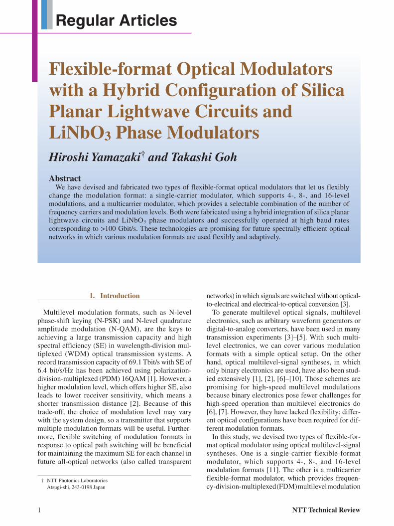
The optical-circuit configuration of the modulator is shown in Fig. 1. It has a two-stage lattice configu-ration. In the first stage, each arm has an MZM. In the second stage, the upper arm has two MZMs con-nected in parallel plus a pair of tunable couplers while the lower arm does not have any functional compo-nents. The couplers at the input of the first stage and between the first and second stages are static 3-dB couplers, while the one at the output of the second stage is another tunable coupler. The four MZMs (denoted MZMs �–4) are driven in push-pull condi-tions with different binary data signals, Data �–4, respectively. All data signals have an amplitude of 2Vp, so the MZMs operate as binary-PSK (BPSK) modulators. MZMs 2 and 4 are followed by p/2 phase shifters. The power coupling ratios of the tunable couplers, a:�-a and b:�-b (upper to lower arms), as denoted in the figure, are varied for different modula-tion formats. The relative optical phase between the upper and lower arms of the second stage, j, is also varied.
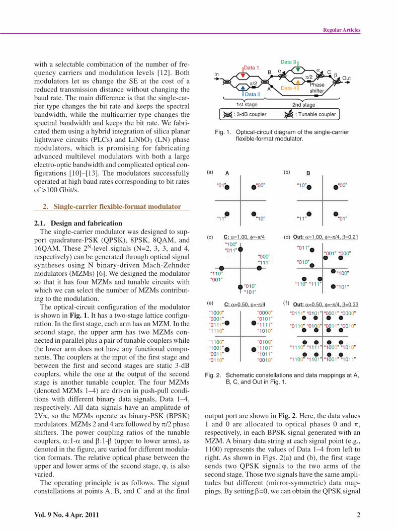
The operating principle is as follows. The signal constellations at points A, B, and C and at the final
output port are shown in Fig. 2. Here, the data values � and 0 are allocated to optical phases 0 and p, respectively, in each BPSK signal generated with an MZM. A binary data string at each signal point (e.g., ��00) represents the values of Data �–4 from left to right. As shown in Figs. 2(a) and (b), the first stage sends two QPSK signals to the two arms of the second stage. Those two signals have the same ampli-tudes but different (mirror-symmetric) data map-pings. By setting b=0, we can obtain the QPSK signal
InData 1
Data 3
Data 2
1st stage
B COut
Phaseshifter
2nd stage
A
: 3-dB coupler : Tunable coupler
π/2π/2
α αβ
Data 4
Fig. 1. Optical-circuit diagram of the single-carrier flexible-format modulator.
(a) A (b) B
(c) C: α=1.00, φ=-π/4 (d) Out: α=1.00, φ=-π/4, β=0.21
(e) C: α=0.50, φ=-π/4 ( f ) Out: α=0.50, φ=-π/4, β=0.33
“01”
“01”
“00” “00”
“11” “11”“10”
“100”“011”
“010”“101”
“110”“001”
“1000”“0001”“0111”“1110”
“1100”“1001”“0011”“0110”
“0000”“0101”“1111”“1010”
“0100”“1101”“1011”“0010”
“000”“111”
“011”
“010”
“001” “000”
“100”
“101”“110” “111”
“10”
“0111” “0101”
“0110” “0100”
“1110” “1111”
“1100” “1101”
“0001” “0000”
“0011” “0010”
“1000” “1010”
“1001” “1011”
Fig. 2. Schematic constellations and data mappings at A, B, C, and Out in Fig. 1.
Regular Articles
3 NTT Technical Review
shown in Fig. 2(a) as the modulator’s final output. An 8QAM signal is generated when a=�, j=-p/4, and b=�/(3+√
−3)≈0.2�. In this case, MZM 3 converts the QPSK signal shown in Fig. 2(b) into the signal shown in Fig. 2(c), in which eight values of 3-bit data degen-erate to four signal points. This double degeneracy is broken when the signals from the upper and lower arms (Figs. 2(c) and (a)) are coupled, and the modula-tor outputs the 8QAM signal shown in Fig. 2(d). An 8PSK signal can also be generated in the same man-ner with a=�, j=-p/2, and b= tan2(p/8)/{�+tan2
(p/8)}≈0.�5. To obtain a �6QAM signal, we set a=0.5, j=-p/4, and b=�/3≈0.33. With this condition, the upper-arm signal has quadruple degeneracy (Fig. 2(e)), which is broken by the coupling with the lower-arm signal (Fig. 2(a)). The final output is the �6QAM signal shown in Fig. 2(f). As described above, we can flexibly switch the modulation level simply by using tunable couplers and a phase shifter. Furthermore, with the lattice configuration, the modulation losses for 8- and �6-level modulations are smaller than those with previously reported schemes [��].
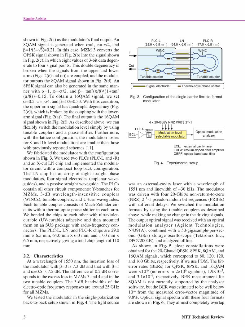
We fabricated the modulator with the configuration shown in Fig. 3. We used two PLCs (PLC-L and -R) and an X-cut LN chip and implemented the modula-tor circuit with a compact loop-back configuration. The LN chip has an array of eight straight phase modulators, four signal electrodes (coplanar wave-guides), and a passive straight waveguide. The PLCs contain all other circuit components: Y-branches for MZMs, 3-dB wavelength-insensitive couplers (WINCs), tunable couplers, and U-turn waveguides. Each tunable coupler consists of Mach-Zehnder cir-cuits with a thermo-optic phase shifter in each arm. We bonded the chips to each other with ultraviolet-curable (UV-curable) adhesive and then mounted them on an SUS package with radio-frequency con-nectors. The PLC-L, LN, and PLC-R chips are 29.0 mm × 6.5 mm, 64.0 mm × 6.0 mm, and �7.0 mm × 6.5 mm, respectively, giving a total chip length of ��0 mm.
2.2. CharacteristicsAt a wavelength of �550 nm, the insertion loss of
the modulator with b=0 is 7.3 dB and that with b=� and a=0.5 is 7.5 dB. The difference of 0.2 dB corre-sponds to the excess loss in MZMs 3 and 4 and in the two tunable couplers. The 3-dB bandwidths of the electro-optic frequency responses are around 25 GHz for all MZMs.
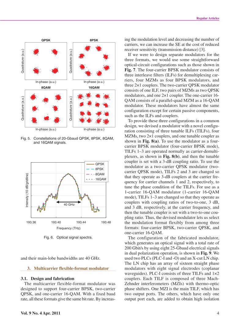
We tested the modulator in the single-polarization back-to-back setup shown in Fig. 4. The light source
was an external-cavity laser with a wavelength of �55� nm and linewidth of ~30 kHz. The modulator was driven with four 20-Gbit/s non-return-to-zero (NRZ) 2��-� pseudo-random bit sequences (PRBSs) with different delays. We switched the modulation formats by using the tunable couplers as described above, while making no change in the driving signals. The output optical signal was received with an optical modulation analyzer (Agilent Technologies, N439�A), combined with a 50-gigasample-per-sec-ond (GS/s) storage oscilloscope (Tektronix Inc., DPO72004B), and analyzed offline.
As shown in Fig. 5, clear constellations were obtained for the 20-Gbaud QPSK, 8PSK, 8QAM, and �6QAM signals, which correspond to 80, �20, �20, and �60 Gbit/s, respectively, if we use PDM. The bit-error rates (BERs) for QPSK, 8PSK, and �6QAM were <�0-6 (no errors in 2�06 symbols), �.9�0-5, and 3.��0-4, respectively. BER measurement for 8QAM is not currently supported by the analyzer software, but the BER was estimated to be well below �0-4 from the measured error-vector magnitude of 9.8%. Optical signal spectra with these four formats are shown in Fig. 6. They almost completely overlap
InWINC WINC
Tunable coupler
Signal electrode Thermo-optic phase shifter
Tunable coupler
PLC-L(29.0 × 6.5 mm)
LN(64.0 × 6.0 mm)
PLC-R(17.0 × 6.5 mm)
Out
Fig. 3. Configuration of the single-carrier flexible-format modulator.
ECL: external cavity laserEDFA: erbium-doped fiber amplifierOBPF: optical bandpass filter
ECLModulation-level-
selectable modulator
4 x 20-Gbit/s NRZ PRBS 211-1
EDFA OBPF Optical modulationanalyzer
Fig. 4. Experimental setup.
Regular Articles
Vol. 9 No. 4 Apr. 2011 4
and their main-lobe bandwidths are 40 GHz.
3. Multicarrier flexible-format modulator
3.1. Design and fabricationThe multicarrier flexible-format modulator was
designed to support four-carrier BPSK, two-carrier QPSK, and one-carrier �6-QAM. With a fixed baud rate, all these formats give the same bit rate. By increas-
ing the modulation level and decreasing the number of carriers, we can increase the SE at the cost of reduced receiver sensitivity (transmission distance) [3].
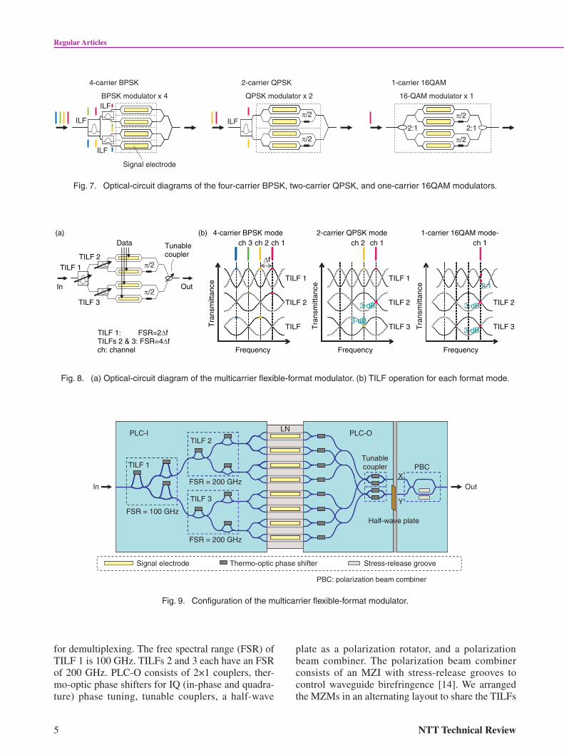
If we were to design separate modulators for the three formats, we would use some straightforward optical-circuit configurations such as those shown in Fig. 7. The four-carrier BPSK modulator consists of three interleave filters (ILFs) for demultiplexing car-riers, four MZMs as four BPSK modulators, and three 2� couplers. The two-carrier QPSK modulator consists of one ILF, two pairs of MZMs as two QPSK modulators, and one 2� coupler. The one-carrier �6-QAM consists of a parallel-quad MZM as a �6-QAM modulator. These modulators have almost the same configuration except for certain passive components, such as the ILFs and couplers.
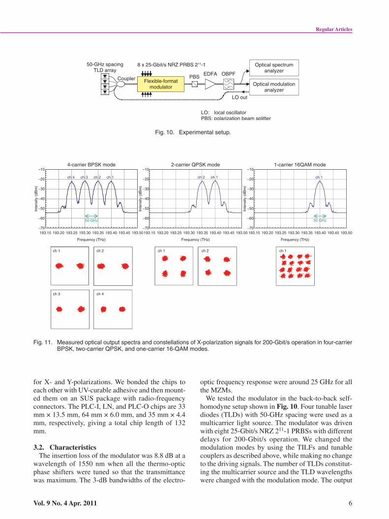
To provide these three configurations in a common design, we devised a modulator with a novel configu-ration consisting of three tunable ILFs (TILFs), four MZMs, two 2×� couplers, and one tunable coupler as shown in Fig. 8(a). To use the modulator as a four-carrier BPSK modulator (four-carrier BPSK mode), TILFs �–3 are operated normally as carrier-demulti-plexers, as shown in Fig. 8(b), and then the tunable coupler is set with a 3-dB coupling ratio. To use the modulator as a two-carrier QPSK modulator (two-carrier QPSK mode), TILFs 2 and 3 are changed so that they operate as 3-dB couplers at the carrier fre-quency for carrier channels � and 2, respectively, to tune the phase condition of the TILFs. For use as a �-carrier �6-QAM modulator (�-carrier �6-QAM mode), TILFs �–3 are changed so that they operate as couplers with coupling ratios of two-to-one, 3 dB, and 3 dB, respectively, at the carrier frequency, and then the tunable coupler is set with a two-to-one cou-pling ratio. Thus, the devised modulator lets us select the modulation format flexibly from among three formats: four-carrier BPSK, two-carrier QPSK, and one-carrier �6-QAM.
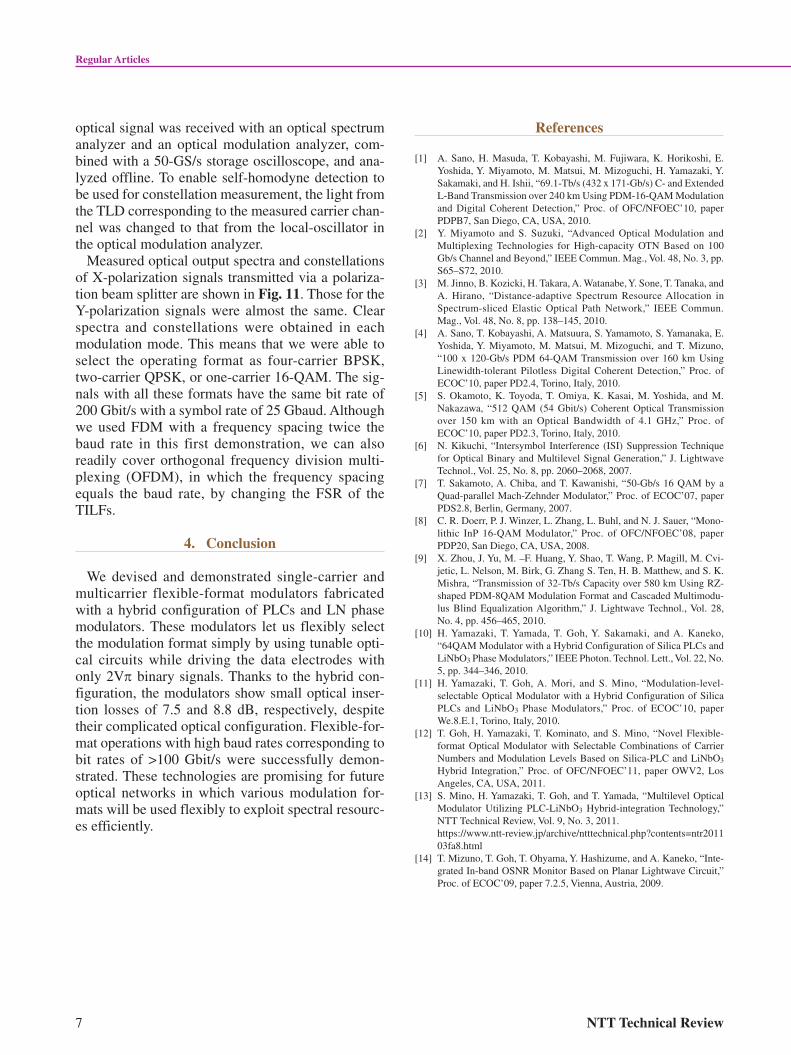
The configuration of the fabricated modulator, which generates an optical signal with a total rate of 200 Gbit/s by using eight 25-Gbaud electrical signals in dual polarization operation, is shown in Fig. 9. We used two PLCs (PLC-I and -O) and an X-cut LN chip. The LN chip has an array of sixteen straight phase modulators with eight signal electrodes (coplanar waveguides). PLC-I consists of three TILFs and �×2 couplers. Each TILF is composed of three Mach- Zehnder interferometers (MZIs) with thermo-optic phase shifters. One MZI is the main TILF, which has two output ports. The others, which have only one output port each, are added to obtain high isolation
In-phase (a.u.)
In-phase (a.u.)In-phase (a.u.)
In-phase (a.u.)
Qua
drat
ure
(a.u
.)Q
uadr
atur
e (a
.u.)
Qua
drat
ure
(a.u
.)Q
uadr
atur
e (a
.u.)
QPSK 8PSK
8QAM 16QAM
Fig. 5. Constellations of 20-Gbaud QPSK, 8PSK, 8QAM, and 16QAM signals.
193.36 193.40
Frequency (THz)
193.44 193.48
Inte
nsity
(10
dB
/grid
line)
QPSK
8PSK
8QAM
16QAM
40 GHz
Fig. 6. Optical signal spectra.
Regular Articles
5 NTT Technical Review
for demultiplexing. The free spectral range (FSR) of TILF � is �00 GHz. TILFs 2 and 3 each have an FSR of 200 GHz. PLC-O consists of 2� couplers, ther-mo-optic phase shifters for IQ (in-phase and quadra-ture) phase tuning, tunable couplers, a half-wave
plate as a polarization rotator, and a polarization beam combiner. The polarization beam combiner consists of an MZI with stress-release grooves to control waveguide birefringence [�4]. We arranged the MZMs in an alternating layout to share the TILFs
π/2
π/2
2:1 2:1
QPSK modulator x 2
π/2
π/2
ILFILF
Signal electrode
BPSK modulator x 4ILF
ILF
16-QAM modulator x 1
4-carrier BPSK 2-carrier QPSK 1-carrier 16QAM
Fig. 7. Optical-circuit diagrams of the four-carrier BPSK, two-carrier QPSK, and one-carrier 16QAM modulators.
TILF 1: FSR=2∆fTILFs 2 & 3: FSR=4∆fch: channel
TILF 1
TILF 2
TILF 3
Tunablecoupler
Data
In OutTILF 1
TILF 2
TILF
1-carrier 16QAM mode-
TILF 1
TILF 2
TILF 3
TILF 2
TILF 3
(a)ch 1ch 2ch 3 ch 2 ch 1 ch 1
Frequency
Tra
nsm
ittan
ce
∆f
4-carrier BPSK mode 2-carrier QPSK mode
Frequency
Tra
nsm
ittan
ce
Frequency
Tra
nsm
ittan
ce
3-dB
3-dB
3-dB
3-dB
2:1
(b)
π/2
π/2
Fig. 8. (a) Optical-circuit diagram of the multicarrier flexible-format modulator. (b) TILF operation for each format mode.
PBC: polarization beam combiner
Signal electrode Thermo-optic phase shifter Stress-release groove
TILF 2
TILF 3
TILF 1 PBCTunablecoupler
FSR = 100 GHz
FSR = 200 GHz
FSR = 200 GHz
Half-wave plate
PLC-I PLC-OLN
In OutX
Y
Fig. 9. Configuration of the multicarrier flexible-format modulator.
Regular Articles
Vol. 9 No. 4 Apr. 2011 6
for X- and Y-polarizations. We bonded the chips to each other with UV-curable adhesive and then mount-ed them on an SUS package with radio-frequency connectors. The PLC-I, LN, and PLC-O chips are 33 mm × �3.5 mm, 64 mm × 6.0 mm, and 35 mm × 4.4 mm, respectively, giving a total chip length of �32 mm.
3.2. CharacteristicsThe insertion loss of the modulator was 8.8 dB at a
wavelength of �550 nm when all the thermo-optic phase shifters were tuned so that the transmittance was maximum. The 3-dB bandwidths of the electro-
optic frequency response were around 25 GHz for all the MZMs.
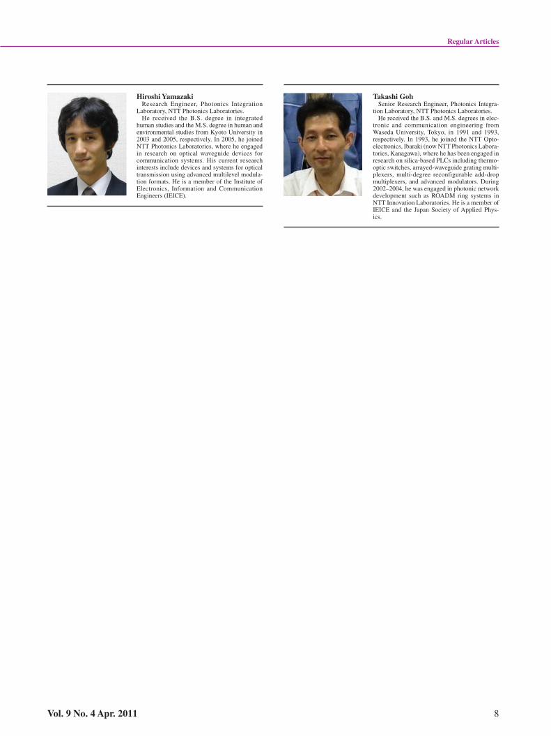
We tested the modulator in the back-to-back self-homodyne setup shown in Fig. 10. Four tunable laser diodes (TLDs) with 50-GHz spacing were used as a multicarrier light source. The modulator was driven with eight 25-Gbit/s NRZ 2��-� PRBSs with different delays for 200-Gbit/s operation. We changed the modulation modes by using the TILFs and tunable couplers as described above, while making no change to the driving signals. The number of TLDs constitut-ing the multicarrier source and the TLD wavelengths were changed with the modulation mode. The output
Optical modulationanalyzer
50-GHz spacingTLD array
LO out
Optical spectrumanalyzer
EDFA OBPFCoupler
8 x 25-Gbit/s NRZ PRBS 211-1
PBS
LO: local oscillatorPBS: polarization beam splitter
Flexible-formatmodulator
Fig. 10. Experimental setup.
4-carrier BPSK mode 2-carrier QPSK mode 1-carrier 16QAM mode−10
−30
−20
−40
−60
−50
−70193.15 193.20
ch 1
Frequency (THz) Frequency (THz) Frequency (THz)
ch 2 ch 1 ch 1ch 2
ch 3 ch 4
193.25 193.30 193.35 193.40 193.45 193.50
Inte
nsity
(dB
m)
Inte
nsity
(dB
m)
Inte
nsity
(dB
m)
−10
−30
−20
−40
−60
−50
−70
−10
−30
−20
−40
−60
−50
−70193.15 193.20 193.25 193.30 193.35 193.40 193.45 193.50 193.15 193.20 193.25 193.30 193.35 193.40 193.45 193.50
50 GHz 50 GHz
ch 4 ch 3 ch 2 ch 1 ch 2 ch 1 ch 1
Fig. 11. Measured optical output spectra and constellations of X-polarization signals for 200-Gbit/s operation in four-carrier BPSK, two-carrier QPSK, and one-carrier 16-QAM modes.
Regular Articles
7 NTT Technical Review
optical signal was received with an optical spectrum analyzer and an optical modulation analyzer, com-bined with a 50-GS/s storage oscilloscope, and ana-lyzed offline. To enable self-homodyne detection to be used for constellation measurement, the light from the TLD corresponding to the measured carrier chan-nel was changed to that from the local-oscillator in the optical modulation analyzer.
Measured optical output spectra and constellations of X-polarization signals transmitted via a polariza-tion beam splitter are shown in Fig. 11. Those for the Y-polarization signals were almost the same. Clear spectra and constellations were obtained in each modulation mode. This means that we were able to select the operating format as four-carrier BPSK, two-carrier QPSK, or one-carrier �6-QAM. The sig-nals with all these formats have the same bit rate of 200 Gbit/s with a symbol rate of 25 Gbaud. Although we used FDM with a frequency spacing twice the baud rate in this first demonstration, we can also readily cover orthogonal frequency division multi-plexing (OFDM), in which the frequency spacing equals the baud rate, by changing the FSR of the TILFs.
4. Conclusion
We devised and demonstrated single-carrier and multicarrier flexible-format modulators fabricated with a hybrid configuration of PLCs and LN phase modulators. These modulators let us flexibly select the modulation format simply by using tunable opti-cal circuits while driving the data electrodes with only 2Vp binary signals. Thanks to the hybrid con-figuration, the modulators show small optical inser-tion losses of 7.5 and 8.8 dB, respectively, despite their complicated optical configuration. Flexible-for-mat operations with high baud rates corresponding to bit rates of >�00 Gbit/s were successfully demon-strated. These technologies are promising for future optical networks in which various modulation for-mats will be used flexibly to exploit spectral resourc-es efficiently.
References
[�] A. Sano, H. Masuda, T. Kobayashi, M. Fujiwara, K. Horikoshi, E. Yoshida, Y. Miyamoto, M. Matsui, M. Mizoguchi, H. Yamazaki, Y. Sakamaki, and H. Ishii, “69.�-Tb/s (432 x �7�-Gb/s) C- and Extended L-Band Transmission over 240 km Using PDM-�6-QAM Modulation and Digital Coherent Detection,” Proc. of OFC/NFOEC’�0, paper PDPB7, San Diego, CA, USA, 20�0.
[2] Y. Miyamoto and S. Suzuki, “Advanced Optical Modulation and Multiplexing Technologies for High-capacity OTN Based on �00 Gb/s Channel and Beyond,” IEEE Commun. Mag., Vol. 48, No. 3, pp. S65–S72, 20�0.
[3] M. Jinno, B. Kozicki, H. Takara, A. Watanabe, Y. Sone, T. Tanaka, and A. Hirano, “Distance-adaptive Spectrum Resource Allocation in Spectrum-sliced Elastic Optical Path Network,” IEEE Commun. Mag., Vol. 48, No. 8, pp. �38–�45, 20�0.
[4] A. Sano, T. Kobayashi, A. Matsuura, S. Yamamoto, S. Yamanaka, E. Yoshida, Y. Miyamoto, M. Matsui, M. Mizoguchi, and T. Mizuno, “�00 x �20-Gb/s PDM 64-QAM Transmission over �60 km Using Linewidth-tolerant Pilotless Digital Coherent Detection,” Proc. of ECOC’�0, paper PD2.4, Torino, Italy, 20�0.
[5] S. Okamoto, K. Toyoda, T. Omiya, K. Kasai, M. Yoshida, and M. Nakazawa, “5�2 QAM (54 Gbit/s) Coherent Optical Transmission over �50 km with an Optical Bandwidth of 4.� GHz,” Proc. of ECOC’�0, paper PD2.3, Torino, Italy, 20�0.
[6] N. Kikuchi, “Intersymbol Interference (ISI) Suppression Technique for Optical Binary and Multilevel Signal Generation,” J. Lightwave Technol., Vol. 25, No. 8, pp. 2060–2068, 2007.
[7] T. Sakamoto, A. Chiba, and T. Kawanishi, “50-Gb/s �6 QAM by a Quad-parallel Mach-Zehnder Modulator,” Proc. of ECOC’07, paper PDS2.8, Berlin, Germany, 2007.
[8] C. R. Doerr, P. J. Winzer, L. Zhang, L. Buhl, and N. J. Sauer, “Mono-lithic InP �6-QAM Modulator,” Proc. of OFC/NFOEC’08, paper PDP20, San Diego, CA, USA, 2008.
[9] X. Zhou, J. Yu, M. –F. Huang, Y. Shao, T. Wang, P. Magill, M. Cvi-jetic, L. Nelson, M. Birk, G. Zhang S. Ten, H. B. Matthew, and S. K. Mishra, “Transmission of 32-Tb/s Capacity over 580 km Using RZ-shaped PDM-8QAM Modulation Format and Cascaded Multimodu-lus Blind Equalization Algorithm,” J. Lightwave Technol., Vol. 28, No. 4, pp. 456–465, 20�0.
[�0] H. Yamazaki, T. Yamada, T. Goh, Y. Sakamaki, and A. Kaneko, “64QAM Modulator with a Hybrid Configuration of Silica PLCs and LiNbO3 Phase Modulators,” IEEE Photon. Technol. Lett., Vol. 22, No. 5, pp. 344–346, 20�0.
[��] H. Yamazaki, T. Goh, A. Mori, and S. Mino, “Modulation-level-selectable Optical Modulator with a Hybrid Configuration of Silica PLCs and LiNbO3 Phase Modulators,” Proc. of ECOC’�0, paper We.8.E.�, Torino, Italy, 20�0.
[�2] T. Goh, H. Yamazaki, T. Kominato, and S. Mino, “Novel Flexible-format Optical Modulator with Selectable Combinations of Carrier Numbers and Modulation Levels Based on Silica-PLC and LiNbO3 Hybrid Integration,” Proc. of OFC/NFOEC’��, paper OWV2, Los Angeles, CA, USA, 20��.
[�3] S. Mino, H. Yamazaki, T. Goh, and T. Yamada, “Multilevel Optical Modulator Utilizing PLC-LiNbO3 Hybrid-integration Technology,” NTT Technical Review, Vol. 9, No. 3, 20��.
https://www.ntt-review.jp/archive/ntttechnical.php?contents=ntr20��03fa8.html
[�4] T. Mizuno, T. Goh, T. Ohyama, Y. Hashizume, and A. Kaneko, “Inte-grated In-band OSNR Monitor Based on Planar Lightwave Circuit,” Proc. of ECOC’09, paper 7.2.5, Vienna, Austria, 2009.
Regular Articles
Vol. 9 No. 4 Apr. 2011 8
Hiroshi YamazakiResearch Engineer, Photonics Integration
Laboratory, NTT Photonics Laboratories.He received the B.S. degree in integrated
human studies and the M.S. degree in human and environmental studies from Kyoto University in 2003 and 2005, respectively. In 2005, he joined NTT Photonics Laboratories, where he engaged in research on optical waveguide devices for communication systems. His current research interests include devices and systems for optical transmission using advanced multilevel modula-tion formats. He is a member of the Institute of Electronics, Information and Communication Engineers (IEICE).
Takashi GohSenior Research Engineer, Photonics Integra-
tion Laboratory, NTT Photonics Laboratories.He received the B.S. and M.S. degrees in elec-
tronic and communication engineering from Waseda University, Tokyo, in �99� and �993, respectively. In �993, he joined the NTT Opto-electronics, Ibaraki (now NTT Photonics Labora-tories, Kanagawa), where he has been engaged in research on silica-based PLCs including thermo-optic switches, arrayed-waveguide grating multi-plexers, multi-degree reconfigurable add-drop multiplexers, and advanced modulators. During 2002–2004, he was engaged in photonic network development such as ROADM ring systems in NTT Innovation Laboratories. He is a member of IEICE and the Japan Society of Applied Phys-ics.