Embed Size (px)
Citation preview

ARTICLE
Received 7 Oct 2013 | Accepted 15 Jan 2014 | Published 7 Feb 2014
Fractal design concepts for stretchable electronicsJonathan A. Fan1,2,*, Woon-Hong Yeo1,3,*, Yewang Su4,5,*, Yoshiaki Hattori1, Woosik Lee1, Sung-Young Jung6,
Yihui Zhang4,5, Zhuangjian Liu7, Huanyu Cheng4, Leo Falgout1, Mike Bajema8, Todd Coleman8, Dan Gregoire9,
Ryan J. Larsen2, Yonggang Huang4 & John A. Rogers1,2
Stretchable electronics provide a foundation for applications that exceed the scope of
conventional wafer and circuit board technologies due to their unique capacity to integrate
with soft materials and curvilinear surfaces. The range of possibilities is predicated on the
development of device architectures that simultaneously offer advanced electronic function
and compliant mechanics. Here we report that thin films of hard electronic materials
patterned in deterministic fractal motifs and bonded to elastomers enable unusual mechanics
with important implications in stretchable device design. In particular, we demonstrate the
utility of Peano, Greek cross, Vicsek and other fractal constructs to yield space-filling
structures of electronic materials, including monocrystalline silicon, for electrophysiological
sensors, precision monitors and actuators, and radio frequency antennas. These devices
support conformal mounting on the skin and have unique properties such as invisibility under
magnetic resonance imaging. The results suggest that fractal-based layouts represent
important strategies for hard-soft materials integration.
DOI: 10.1038/ncomms4266
1 Department of Materials Science and Engineering, University of Illinois at Urbana-Champaign, 104 South Goodwin Ave, Urbana, Illinois 61801, USA.2 Beckman Institute for Advanced Science and Technology, 405 N. Mathews M/C 251, Urbana, Illinois 61801, USA. 3 Department of Mechanical and NuclearEngineering, Virginia Commonwealth University, 401 West Main St, Richmond, Virginia 23284, USA. 4 Departments of Civil and Environmental Engineeringand Mechanical Engineering, Center for Engineering and Health, Skin Disease Research Center, Northwestern University, 2145 Sheridan Road, Evanston,Illinois 60208, USA. 5 Center for Mechanics and Materials, Tsinghua University, Beijing 100084, China. 6 Department of Mechanical Engineering, PohangUniversity of Science and Technology, Pohang 790-784, Republic of Korea. 7 Institute of High Performance Computing, A*Star, Singapore 138632, Singapore.8 Department of Bioengineering, University of California, San Diego, 9500 Gilman Drive MC 0412, La Jolla, California 92093, USA. 9 HRL Laboratories, LLC,3011 Malibu Canyon Road, Malibu, California 90265, USA. * These authors contributed equally to this work. Correspondence and requests for materialsshould be addressed to J.A.R. (email: [email protected]).
NATURE COMMUNICATIONS | 5:3266 | DOI: 10.1038/ncomms4266 | www.nature.com/naturecommunications 1
& 2014 Macmillan Publishers Limited. All rights reserved.

The field of stretchable electronics is of growing interest1,2,motivated both by fundamental considerations inmaterial science and by application spaces in areas such
as biomedicine3–6. A core challenge is in achieving high-performance electronic functionality with systems that offerelastic, low modulus responses to large strain deformations. Twoof the most successful approaches to this problem exploitadvanced composites, in a generalized sense. The first involvesdispersing conducting or semiconducting nanomaterials (that is,nanowires, nanotubes or graphene) into elastomeric matrices7–11.Here, three-dimensional (3D) structures, including distributednetworks of contacts, form spontaneously, but with limited directcontrol over key variables other than the overall loading fraction.The second exploits alternative classes of composites, createddeterministically by using thin layers of electronic materialslithographically defined into two dimensional (2D) filamentarymesh layouts12–14. Advantages of this approach include theability to co-integrate multiple high-performance materialplatforms with high spatial resolution and engineering control,in ways that also allow proper electrical contacts, both internaland external to the system15. An essential aim of both3D random and 2D deterministic composites in stretchableelectronics is to combine high loading of a hard component, foruse in active devices, with overall mechanics that is dominated bya soft matrix, for stretchable response. This goal is opposite tothat associated with traditional composites engineering andtherefore demands alternative approaches.
Here, we show that concepts in fractal geometry, whichare known to determine behaviours in traditional 3D
networks16–20 and which are pervasive in biological systemsincluding the human body21,22, can be successfully exploited in2D deterministic systems, with important functionalconsequences in advanced stretchable electronics. Fractal-basedstructures can be described by self-similarity: subdivision intosmall sections yields pieces with geometries that resemble thewhole. Compared with previously explored networks of periodicserpentine shapes, fractal designs can be engineered toaccommodate enhanced elastic strain along a selecteddimension and to support biaxial, radial and other deformationmodes. In addition, the choices of topologies span a rich range,from lines to loops, capable of tailoring to specific electronicapplications through integration and interdigitation of multiplestructures. Figure 1 presents six representative examples, fromlines (Koch, Peano, Hilbert) to loops (Moore, Vicsek) andbranch-like meshes (Greek cross). The results illustrate thediversity of possibilities, through both the finite element method(FEM) and experimental demonstration. The approximate fractaldimensions in these finite-iterative curves range from 1.5 to 2.The elastic tensile strains achieved with these structures indicatethat they are suitable for use in various stretchable devices,including the epidermal electronic platform23, with keyadvantages over previously described layouts.
ResultsMechanics and electronics with Peano-based geometries. ThePeano curve24 provides a model system for examining thedetailed mechanics of fractal-based motifs. Layouts using these or
von Koch curve Peano curve Hilbert curve Moore curve Vicsek fractal Greek cross
0.0
0.3�max (%)
55% strain 75% strain 40% strain 35% strain 35% strain 35% strain
Figure 1 | Representative fractal-inspired layouts for hard-soft materials integration. (a) Six different patterns of metal wires fully bonded to
elastomer substrates demonstrate the application of deterministic fractal designs as general layouts for stretchable electronics. These patterns include line,
loop and branch-like geometries, and they are applicable to a broad range of active and passive electronic components. In all cases, arc sections replace
the sharp corners from the mathematically defined fractal layouts to improve the elastic mechanics. (b) FEM images of each structure under elastic
tensile strain and (c) their corresponding experimental MicroXCT images demonstrate the elastic mechanics. The wires consist of layers of gold (300 nm)
sandwiched by polyimide (1.2 mm) and mounted on an elastomeric substrate (0.5 mm). Scale bars, 2 mm.
ARTICLE NATURE COMMUNICATIONS | DOI: 10.1038/ncomms4266
2 NATURE COMMUNICATIONS | 5:3266 | DOI: 10.1038/ncomms4266 | www.nature.com/naturecommunications
& 2014 Macmillan Publishers Limited. All rights reserved.

other designs follow an iterative approach to create the Nth Peanocurve, nine copies of the (N� 1)th curve are linked together intoa single line. An illustration of the first three iterations of a Peanocurve appears in Fig. 2a. A physical interpretation that capturesthe underlying mechanics follows by considering the first iterativecurve geometry as a section of a one-dimensional spring. Becauseof self-similarity, higher order Peano curves contain spring-likemotifs at multiple length scales (Supplementary Fig. 1).Furthermore, each of these motifs can be oriented vertically(y-axis) or horizontally (x-axis). As such, the Peano geometryprovides a design metric for systematically ‘folding’ a straight lineinto a compact and stretchable layout. To further enhance themechanics of these wires, arc sections replace the sharp corners inthe mathematically defined Peano curves (Fig. 2b). Generally, theelastic mechanics of horseshoe serpentine structures improvewith increasing arc section angle (Supplementary Table 1).Although the Peano curves featured in Fig. 2a fill square areas,those of different iterative orders can be linked together to fillspaces of arbitrary shape. As a demonstration, Fig. 2c–f show theword ‘ILLINOIS’ formed with space filling wires, in which eachletter consists of a combination of first and second order Peanocurves. The figure includes a detailed view of a section of the ‘N’.Electrodes can be constructed in this manner to match, forexample, particular features on the body.
The Peano curves in Fig. 2a represent only one set ofvariations; there exist many others, because the (N� 1)th unitcells of any Nth order curve can be oriented either vertically orhorizontally (Supplementary Fig. 2). The second order curve has272 unique layouts alone, each with distinct mechanical proper-ties. Numerical simulations of five different second order layouts
consisting of gold wires bonded on an elastomer probe therelationship between mechanics and layout. The layouts containunit cells with orientations ranging from all vertical to allhorizontal (Table 1). The maximum principal strain criteriondefines the maximum elastic stretchability as the onset of plasticyield, consistent with established parameters of the constituentmaterials25. Table 1 summarizes this quantity, calculated foruniaxial deformation along the x- and y-axis. The results indicatethat Peano layouts with unit cells all oriented in the same waymaximize the uniaxial stretchability along the unit cell direction.The ‘half-and-half’ Peano layout, which contains unit cells withalternating orientations, balances the maximum strain supportedalong the x- and y-axis at 16% and 13%, respectively. Suchproperties are well suited for devices that stretch along both axes.Adjustments to the total unit cell size can enhance the mechanicsof these structures (Supplementary Table 2). The third orderhalf-and-half layouts yield stretchabilities along the x- and y-axisof 32% and 28%, respectively (Supplementary Fig. 3). Thisimprovement with iteration order is due to the combined effectsof geometric scaling of the arc sections, increase in the length ofthe wire and addition of higher order spring-like motifs. Thestretchability here is well above 20%, which is the general upperlimit for the elastic mechanics of skin23.
Experimental structures consisting of second and third orderhalf-and-half Peano layouts of metallic wires that are clad withpolyimide and fully bonded to an elastomeric membranecompare well with the numerical analysis (See Methods fordetails). The polyimide cladding retards strain localization in themetal26, thereby enhancing sample yield and consistency in themechanical tests. Three samples are tested for each fractal
Figure 2 | Implementation of Peano curves for stretchable electronics. (a) Illustration of three iterations of a two-dimensional Peano curve. Nine versions
of the (N-1)th curve (dotted red box) connect together with the solid red lines to construct the Nth curve. (b) Arc sections replace the sharp
bends to enhance the mechanics. (c) Image of metal wires with Peano layouts, with an overall geometry that spell out the characters in ‘ILLINOIS’, mounted
on skin. Here, each letter consists of a series of first and second order Peano curves. (d) A detailed section of the N (solid red box) from (c) in block
diagram form (small blocks are first order curves, large blocks are second order curves) and as wires. (e) Optical and (f) scanning electron microscopy
images of third order Peano-based wires on skin and a skin-replica (colorized metal wires), respectively, showing the conformal contact of the wires
on the substrate. Scale bar in (e), 2 mm. Scale bar in (f), 500mm.
NATURE COMMUNICATIONS | DOI: 10.1038/ncomms4266 ARTICLE
NATURE COMMUNICATIONS | 5:3266 | DOI: 10.1038/ncomms4266 | www.nature.com/naturecommunications 3
& 2014 Macmillan Publishers Limited. All rights reserved.

dimension and axis of stretching. Mechanical characterizationinvolves measurements of resistance changes to a precision ofB0.01 ohms with a four-point probe technique performed duringuniaxial tensile stretching. In the elastic regime, the wireresistance before and after cycling between states of no strainand increasing levels of maximum strain (the difference definedas the ‘differential resistance’) does not change. At the onset ofplastic deformation, the wire undergoes a resistance-dependentgeometric change, leading to a small but measurable differentialresistance. Traditional approaches to characterizing plasticity27,28
based on measurements of stress-strain response with atensometer are not suitable because the mechanics of theelastomeric substrates in these systems dominate the response,by design.
Figure 3a–f and Supplementary Fig. 3 summarize the results ofthese studies. The differential resistances measured fromindividual representative devices appear together in each plot.The error bars in the second and third order Peano structureshave magnitudes of 3.7e-5 and 3.3e-5, respectively;Supplementary Note 3 discusses the sources of these errors.Simultaneous measurements of the local temperature account forand calibrate out changes in resistance due to backgroundtemperature fluctuations (See Supplementary Note 2). Themeasurements show that for the second order Peano structuresstretched along the x- and y-axis, the transition from elastic toplastic deformation occurs in the range of 16–20% and 12–16%,respectively. The third order Peano structures undergo an elastic-to-plastic transition in the range of 27–32% for stretching alongboth x- and y-axes. These values of uniaxial stretchability areconsistent with the numerical analysis. Calculated FEM images ofstrain localized in the stretched structures (Fig. 3c,d) display thepositions of the mechanical ‘hot spots’ in the samples, wherestrains are particularly large and where failure occurs. Furtherenhancements in device mechanics are possible by optimizing thedetailed geometry of these hot spots.
Fractal-based structures bonded to pre-strained elastomersenable higher levels of elastic deformation29,30. A second orderall-vertical Peano structure fully bonded onto an elastomericsubstrate with 40% pre-strain demonstrates the concept. Thedifferential resistances for different levels of maximum appliedstrain appear in Supplementary Fig. 4. Here, the transition fromelastic to plastic deformation occurs when the substrate isstrained in the range of 60–70%, which is significantly higherthan that in samples prepared without pre-strain. Schemes thatuse pre-strain can be extended to biaxial, radial or other types ofdeformation.
This concept of enhancing mechanics through the use ofpre-strain is general to a broad range of materials, including
semiconductors. Thin films of single crystalline silicon nanomem-branes (Si NM) with two different second order Peano layouts andbonded onto 40% pre-strained elastomeric substrates provide aproof of concept. In the pre-strained state, the calculatedcompressive stresses in the membrane are well within the regimeof elastic deformation for silicon. Figure 3g,h shows microscaleX-ray coherent tomography (microXCT, see SupplementaryNote 1) images of the samples, along with corresponding FEMresults. The findings indicate that the all-vertical and half-and-halfstructures can be elastically strained by 105% and 63%,respectively, given a maximum principal strain of 1% in thesilicon31. The fracture points measured electrically from half-and-half structures (Supplementary Fig. 5) are consistent with the FEMresults. Both the microXCT and FEM images reveal microscalebuckling; this type of deformation mode improves the ability ofthe Si NMs to dissipate stress. Such behaviour persists only for alimited range of NM thicknesses. FEM simulations show that, withincreasing membrane thickness, the NMs transition from a regimeof wrinkling to microscale buckling and finally to global buckling;furthermore, the microscale buckling regime yields maximalelastic mechanics (Supplementary Fig. 6). As such, theoptimization of the elastic properties of hard-soft systemsrequires careful attention to micro-mechanics.
Fractal-based epidermal electronics. The Peano and other fractallayouts have utility for various applications. One is in skin-mounted sensors and actuators such as temperature sensors,heaters and electrodes (Supplementary Fig. 7). Electrodesmeasure electrophysiological processes in the brain (electro-encephalograms (EEGs))23, heart (electrocardiograms (ECGs))and muscle (electromyograms (EMGs))32,33. To minimizeimpedance between the electrode and skin and to optimize themeasured signal-to-noise, electrodes require both conformal skincontact and high areal coverage32,33. Electrodes that interfacedirectly with neurons additionally benefit from having largeperimeters within an area34–36. These needs can be addressedeffectively using a variant of the Greek cross fractal, whichconsists of a hierarchy of cross structures that fills space in twodimensions (Supplementary Fig. 8). This design embeds a highlevel of connectivity, which minimizes the resistance between anytwo points. In addition, defects in the structure, such as linebreaks, have a reduced probability for significantly affectingdevice performance, which is desirable for robust, long-termhealth monitoring in practice33. These geometries can be furtherdesigned to eliminate closed loops (Supplementary Fig. 8), suchthat the edges of the electrode wire layout form a singlecontinuous line. A multifunctional device that incorporates a
Table 1 | Elastic mechanics of five different Peano-based wire structures.
All-Horizontal
Mostly-Horizontal
Half-and-HalfMostly- Vertical
All-Vertical
Config.
x-axis 31% 16% 16% 11% 9%y-axis 9% 12% 13% 14% 33%
Calculated stretchability of metal wires mounted on an elastomer in five different second order Peano layouts, given a maximum principal strain criterion of 0.3% in any section of the wires. The layoutsrange from ‘all-horizontal’ (subunits are all oriented along the x-axis) to ‘all-vertical’ (subunits are all oriented along the y-axis). The strain criterion defines the transition from elastic to plasticdeformation in the wires.
ARTICLE NATURE COMMUNICATIONS | DOI: 10.1038/ncomms4266
4 NATURE COMMUNICATIONS | 5:3266 | DOI: 10.1038/ncomms4266 | www.nature.com/naturecommunications
& 2014 Macmillan Publishers Limited. All rights reserved.

resistive temperature sensing/heating element with an integratedelectrode (recording, ground and reference components together)exploits this feature30 (Fig. 4a). The temperature sensor37 consistsof an insulated line of metal running along the edges of the Greekcross electrode. Figure 4b–f shows a representative device and itsoperation under different modes (heating, temperature sensing,ECG measurements). The impedances and signal-to-noisemeasured with these dry electrodes compare favourably to thatof conventional gel-based electrodes (Supplementary Fig. 9),indicating that they are suitable for high quality, skin-mounted,electrophysiological measurements. The precision of thetemperature measurement (B20 mK) compares well with thatof an infrared camera.
Radio-frequency devices with fractal layouts. Stretchable radiofrequency antennas, which are broadly applicable as mechani-cally-tunable electronic components38,39, are another class ofdevices that benefit from concepts in fractal design. Fractalantennas have been a topic of interest because they can supportmultiband operation in spatial scales that are compact relative tothe resonant wavelength40–42. Appropriate choices of fractallayout offer not only this characteristic but also attractive elasticmechanics when mounted on stretchable substrates. A Vicsekcurve loop antenna (Supplementary Fig. 10), in which arcsections replace sharp bends, provides a model system. Theantenna consists of copper traces (3 mm thick) laminated withpolyimide, and bonded onto a 1 mm thick elastomeric substrate.
Unstrained 15% 30%
FE
ME
xper
imen
t
–1
0
1
2
3
3223 2718149
Rel
ativ
e ch
ange
in r
esis
tanc
e (1
0–4)
Applied strain along x-axis (%)
5
4 8 12 16–0.8
–0.4
0.0
0.4
0.8
1.2
Rel
ativ
e re
sist
ance
chan
ge (
10–4
)Applied strain along x-axis (%)
Exp. plastic transition: 12–16%Theoretical transition: 16%
Exp. plastic transition: 27–32%Theoretical transition: 32%
Unstrained 7.5%
Stretching in x direction
15%
FE
ME
xper
imen
t
0.0
0.3�max (%)
0.0
0.3
�max (%)
‘All vertical’ Peano silicon nanomembrane
Exp
erim
ent
FE
M
0
1�max (%)
‘Half-and-half’ Peano silicon nanomembrane
Exp
erim
ent
FE
M
0
1�max (%)
Stretching in x direction
Stretched (100%)Released Stretched (50%)Released
Second-order Peano gold nanomembrane
Third-order Peano gold nanomembrane
Figure 3 | Mechanics of metal and semiconductor fractal-based structures. (a,d) Optical images of metal wires patterned with second and third
order half-and-half Peano layouts. The samples connect to a stretchable set of four wires used for four-point probing. Scale bar, 5 mm. (b,e) Plot of
differential resistances measured at increasing levels of maximum applied strain. The onset of plastic deformation corresponds to the strain at which the
differential resistance is non-zero. (c,f) A comparison between experimental optical images and FEM-constructed images of the second and third
order structures for different levels of stretching. The FEM images display localized areas of high strain in the stretched structures. Scale bar, 3 mm.
(g,h) MicroXCT and FEM images of Si NMs patterned into Peano layouts and fully bonded to a 40% pre-strained elastomeric substrate. Upon release and
uniaxial stretching, both structures dissipate the mechanical stress via microscale buckles, which is indicative of a mechanical regime well suited for
high levels of elastic deformation. Scale bar, 1 mm.
NATURE COMMUNICATIONS | DOI: 10.1038/ncomms4266 ARTICLE
NATURE COMMUNICATIONS | 5:3266 | DOI: 10.1038/ncomms4266 | www.nature.com/naturecommunications 5
& 2014 Macmillan Publishers Limited. All rights reserved.
The copper thickness is comparable to the skin depth of copper(B2mm) at gigahertz frequencies. The return loss spectrum forthe unstrained antenna displays a fundamental mode near1.7 GHz (Fig. 5a) with an impedance of 42 ohms at resonance.The total length of the antenna at resonance is approximately l0/6,where l0 is the free space wavelength, reflecting the compactnature of this particular fractal layout. As the device is strained, its
fundamental frequency and input impedance slightly shift.Far-field measurements in an anechoic chamber provideadditional information; data for the fundamental mode at 0 and30% strain (Fig. 5c) display a clear dipole-like pattern. The realizedgain for both the unstretched and stretched devices ranges from� 2 to 0 dB, which is slightly less than that for an ideal dipole dueto ohmic losses in the thin copper wires. Simulations of the return
75°C
23
Electrode (recording, ground, and reference)Temperature sensor/heater
Time (s)
Am
plitu
de (
mV
)
0 300
1
10Recording ReferenceGround
Tem
pera
ture
(°C
)
32.4
32.5
32.6
32.7
32.8IR cameraFractaldevice
Time (s)0 3010
Figure 4 | Fractal-based epidermal devices. (a) Schematic image of a multifunctional device based on a Greek cross fractal design, with corresponding
images of the device on a wafer (b) and mounted on skin (c). The device has multiple operation modes, including those for (d) Joule heating, by
driving currents through the insulated heater wires, (e) temperature sensing via four-point probing, and (f) ECG measurements, in which the patch
integrates the recording, reference and ground electrodes. Scale bars in (a) and (b), 2 mm. Scale bars in (c) and (d), 5 mm.
1.0 1.4 1.8 2.2
–25
–20
–15
–10
–5
0
S11
(dB
)
Frequency (GHz)
0%10%20%30%
x
y
z
–30–25–20–15 –10 –5 0
30
210
60
240
90270
120
300
150
330
180
0
xz, unstretched
yz, unstretched
xz, stretched
yz, stretched
0.0
0.3
�max (%)
6
5
7
1 2 3 4
1
2
3
4
5
6
7
Figure 5 | RF properties of stretchable fractal structures. (a) Return loss parameters of a box fractal antenna under different amounts of tensile strain.
Inset: optical image of an unstrained antenna fully bonded onto an elastomer. Scale bar, 4 mm. (b) Optical image of a box fractal antenna under 30%
tensile strain and a corresponding FEM-constructed image of the same structure. Scale bar, 4 mm. (c) Far-field profiles of the antenna under no strain and
30% strain. (d) Cross-sectional MRI image of different copper samples (labelled 1-7) attached to a bottle of water. The solid and mesh samples
display shadowing in the MRI image, while the fractal-based samples display no such shadowing. The sample layouts all are 1� 1 inches and are (1) solid
square, (2) thick mesh, (3) thin mesh, (4) horizontal and vertical stripes separated by a spacer, (5) Peano curve, (6) Hilbert curve, (7) Serpentine Greek
cross. Scale bar, 5 mm.
ARTICLE NATURE COMMUNICATIONS | DOI: 10.1038/ncomms4266
6 NATURE COMMUNICATIONS | 5:3266 | DOI: 10.1038/ncomms4266 | www.nature.com/naturecommunications
& 2014 Macmillan Publishers Limited. All rights reserved.

losses and far field profiles are consistent with the experiments(Supplementary Fig. 11, Supplementary Note 4).
Another application that can benefit from the favourable RFproperties and mechanics of fractal patterns is in electrodestructures that are compatible with magnetic resonance imaging(MRI). Copper foil samples mounted onto a cylindrical phantomand scanned in a 3-Tesla Trio head scanner (Siemens Instriuments)provide a demonstration. For purposes of comparison, the samplesinclude three types of fractals, along with an unpatterned sheet, twovariants of serpentine meshes, and superimposed vertical andhorizontal lines. The fill fraction of the meshes and the fractalpatterns are approximately the same (B25%). For the magneticfield strength used here, the resonant RF pulse frequencies areB123 MHz. Figure 5d displays an axial cross-sectional scanobtained using a spin echo imaging sequence (parameters are inSupplementary Note 5). The water-based phantom appears whitedue to its high hydrogen concentration. The MRI image shows clearshadows in the vicinity of the unpatterned film and the meshsamples. Conversely, the fractal samples exhibit no noticeabledistortion or shadowing. Magnetostatic coupling between RFradiation and the samples, which yields circulating currents andassociated heat dissipation and signal loss, explains thesedifferences. The meshes couple to RF radiation because they consistof highly interconnected closed loops of metal; in contrast, thefractals do not contain closed loops, do not couple to RF radiationand are invisible in the MRI. This analysis suggests that fractal-based designs provide routes to MRI-compatible skin-mounted orimplanted electronic devices.
In summary, fractal-based layouts create new design opportu-nities in stretchable electronics, including a broad range of devicessuitable for biomedical systems. One of the challenges here isevaluating the mechanical properties of these composite materialsand rigorously identifying their elastic and plastic mechanics.With the combination of high precision electro-mechanicalmeasurements and three-dimensional FEM simulations, thefundamental mechanical responses and their dependence ongeometry can be understood and exploited for specific deforma-tion modes. This study suggests a general relationship betweenfractal layouts and mechanics that is broadly applicable tostretchable materials engineering.
MethodsEpidermal device fabrication. Fabrication of metal-based devices, including thetemperature sensors and heaters, involves first spin-coating and curing liquidpolyimide (PI) on a UV-treated PDMS-coated Si wafer. Electron beam evaporationyields layers of chromium (4 nm) and gold (300 nm). Following metal patterning,etching and the application of a second layer of polyimide, a photoresist mask andoxygen plasma etch define the polyimide-encapsulated device. All of the wires are70mm wide and the polyimide layers are each 1.2 mm thick. Water-soluble tape(3 M) retrieves the gold-polyimide structures, which covalently attach to an elas-tomer (0.5 mm thick, Ecoflex or Solaris, Smooth-on Inc.) using an evaporatedchromium-silica bonding layer. UV radiation pretreatment of the elastomer pro-motes covalent bonding between the silica and elastomer. An ACF cable (Elform,USA) attached to the bonding pads of the device enable accessible electricaladdressing. The same process, with an additional polyimide etch step, applies to theopen metal-based fractal electrodes for electrophysiological sensing.
An SOI wafer consisting of 260 nm thick p-doped silicon on a 1 mm thick silicondioxide layer is the starting point for the Si NM samples. To detach the Si NMsfrom the handle wafer, an HF wet etch dissolves the underlying silicon dioxidethrough an array of 3 mm wide holes defined in the membranes. A PDMS stamptransfers the membranes onto a polyimide film, and a photoresist mask and dryetching process define the membranes into various Peano layouts. Gold wireselectrically address the devices, and the same transfer steps described above finalizethe devices.
Antenna fabrication. The starting material is copper foil (3 mm) on a coppercarrier (35 mm; Olin Brass). Polyimide spun-cast and cured onto the foil yield foil-polyimide laminates, which mount onto a PDMS-coated substrate and enablecopper carrier removal. A photoresist mask, wet copper etch and oxygen plasmadry etch pattern the antenna.
Fractal-based metal wire simulations. FEM yields the theoretical deformation,elastic-to-plastic transition and fracture of the structures. For simulations presentedin Figs 1 and 3 and Table 1, the elastomeric substrates employ an 8-node, hex-ahedral brick solid element C3D8R in the FEM programme, and the thin wires ofPI/Au/PI-layered geometry employ a quadrilateral shell element S4R with thesection of composite layup. All of the wires are 70 mm wide and consist of a 300 nmthick gold layer sandwiched by 1.2 mm thick polyimide layers on each side. Thetotal pattern areas are 7 by 7 mm and fully bond to a 0.5 mm thick elastomer with amodulus of 50 kPa. The solid elements bond together physically and thereforeshare nodes with its adhered shell elements. An ideal elastic-plastic constitutiverelation with a Young’s modulus of 78 GPa, Poisson’s ratio of 0.44, yield strain of0.3% and fracture strain of 5% describe the mechanical behaviour of Au. Theelastic-plastic transition is set when the maximum strain of half the width of onesection is beyond the yield strain of 0.3%.
Electrode and temperature sensor testing. The Greek cross electrodes recordECG signals from the torso. Scotch tape exfoliates the stratum corneum and analcohol swab removes dirt or particles to reduce effects of hydration and surfaceimpedance. Here, the ground electrode, located between the measurement andreference electrodes (B7 mm apart at center-to-center distance), defines thecommon zero potential. Measured signals transmit wirelessly to a receiver, andcommercial software using a 60 Hz notch filter and low-pass Butterworth filters(BioRadio 150, Cleveland Medical Devices, USA) completes the analysis. Thefractal temperature sensors operate using the same four-point probe techniquedescribed in the mechanical testing section. An IR camera and hot plate yields dV/dT used to calibrate the devices. The devices mount directly onto the skin with noelastomeric backing layer with a spray bandage technique.
References1. Rogers, J. A., Someya, T. & Huang, Y. G. Materials and mechanics for
stretchable electronics. Science 327, 1603–1607 (2010).2. Wagner, S. & Bauer, S. Materials for stretchable electronics. MRS Bull. 37,
207–217 (2012).3. Kim, D. H., Ghaffari, R., Lu, N. S. & Rogers, J. A. in Annual Review of
Biomedical Engineering Vol. 14 (ed Yarmush, M. L.) 113–128 (Annual Reviews,2012).
4. Tian, B. Z. et al. Macroporous nanowire nanoelectronic scaffolds for synthetictissues. Nat. Mater. 11, 986–994 (2012).
5. Takei, K. et al. Nanowire active-matrix circuitry for low-voltage macroscaleartificial skin. Nat. Mater. 9, 821–826 (2010).
6. Ramuz, M., Tee, B. C. K., Tok, J. B. H. & Bao, Z. Transparent, optical, pressure-sensitive artificial skin for large-area stretchable electronics. Adv. Mater. 24,3223–3227 (2012).
7. Sekitani, T. et al. A rubberlike stretchable active matrix using elasticconductors. Science 321, 1468–1472 (2008).
8. Ahn, B. Y. et al. Omnidirectional printing of flexible, stretchable, and spanningsilver microelectrodes. Science 323, 1590–1593 (2009).
9. Wu, H. et al. A transparent electrode based on a metal nanotrough network.Nat. Nanotechnol. 8, 421–425 (2013).
10. Sekitani, T. et al. Stretchable active-matrix organic light-emitting diode displayusing printable elastic conductors. Nat. Mater. 8, 494–499 (2009).
11. Robinson, A. P., Minev, I., Graz, I. M. & Lacour, S. P. Microstructured siliconesubstrate for printable and stretchable metallic films. Langmuir 27, 4279–4284(2011).
12. Gray, D. S., Tien, J. & Chen, C. S. High-conductivity elastomeric electronics.Adv. Mater. 16, 393–397 (2004).
13. Brosteaux, D., Axisa, F., Gonzalez, M. & Vanfleteren, J. Design and fabricationof elastic interconnections for stretchable electronic circuits. IEEE ElectronDevice Lett. 28, 552–554 (2007).
14. Vanfleteren, J. et al. Printed circuit board technology inspired stretchablecircuits. MRS Bull. 37, 254–260 (2012).
15. Kim, D. H., Xiao, J. L., Song, J. Z., Huang, Y. G. & Rogers, J. A. Stretchable,curvilinear electronics based on inorganic materials. Adv. Mater. 22, 2108–2124(2010).
16. Chen, Z. & Mecholsky, J. J. Control of strength and toughness of ceramic-metallaminates using interface design. J. Mater. Res. 8, 2362–2369 (1993).
17. Connor, M. T., Roy, S., Ezquerra, T. A. & Calleja, F. J. B. Broadband acconductivity of conductor-polymer composites. Phys. Rev. B 57, 2286–2294(1998).
18. Hajji, P., David, L., Gerard, J. F., Pascault, J. P. & Vigier, G. Synthesis, structure,and morphology of polymer-silica hybrid nanocomposites based onhydroxyethyl methacrylate. J. Polymer Sci. Part B-Polymer Phys. 37, 3172–3187(1999).
19. Kim, Y. et al. Stretchable nanoparticle conductors with self-organizedconductive pathways. Nature 500, 59–63 (2013).
20. Zhang, M. Q., Lu, Z. P. & Friedrich, K. On the wear debris ofpolyetheretherketone: Fractal dimensions in relation to wear mechanisms.Tribol. Int. 30, 87–102 (1997).
NATURE COMMUNICATIONS | DOI: 10.1038/ncomms4266 ARTICLE
NATURE COMMUNICATIONS | 5:3266 | DOI: 10.1038/ncomms4266 | www.nature.com/naturecommunications 7
& 2014 Macmillan Publishers Limited. All rights reserved.

21. Goldberger, A. L. & West, B. J. Fractals in Physiology and Medicine. Yale J. Biol.Med. 60, 421–435 (1987).
22. Masters, B. R. Fractal analysis of the vascular tree in the human retina. Ann.Rev. Biomed. Eng. 6, 427–452 (2004).
23. Kim, D. H. et al. Epidermal electronics. Science 333, 838–843 (2011).24. Sagan, H. Space-filling curves (Springer-Verlag, 1994).25. Chasiotis, I. et al. Strain rate effects on the mechanical behavior of
nanocrystalline Au films. Thin Solid Films 515, 3183–3189 (2007).26. Lu, N. S., Wang, X., Suo, Z. G. & Vlassak, J. Metal films on polymer substrates
stretched beyond 50%. Appl. Phys. Lett. 91, 221909 (2007).27. Espinosa, H. D., Prorok, B. C. & Peng, B. Plasticity size effects in free-standing
submicron polycrystalline FCC films subjected to pure tension. J. Mech. Phys.Solids. 52, 667–689 (2004).
28. Chasiotis, I. & Knauss, W. G. A new microtensile tester for the study of MEMSmaterials with the aid of atomic force microscopy. Exp. Mech. 42, 51–57 (2002).
29. Jiang, H. et al. Finite deformation mechanics in buckled thin films oncompliant supports. Proc. Natl Acad. Sci. USA 104, 15607–15612 (2007).
30. Song, J. et al. Buckling of a stiff thin film on a compliant substrate in largedeformation. Int. J. Solids. Struct. 45, 3107–3121 (2008).
31. Sato, K., Yoshioka, T., Ando, T., Shikida, M. & Kawabata, T. Tensile testing ofsilicon film having different crystallographic orientations carried out on asilicon chip. Sensors and Actuators A: Physical 70, 148–152 (1998).
32. Jeong, J.-W. et al. Materials and optimized designs for human-machineinterfaces via epidermal electronics. Adv. Mater. 25, 6839–6846 (2013).
33. Yeo, W. H. et al. Multifunctional epidermal electronics printed directly onto theskin. Adv. Mater. 25, 2773–2778 (2013).
34. Fairbanks, M. S., McCarthy, D. N., Scott, S. A., Brown, S. A. & Taylor, R. P.Fractal electronic devices: simulation and implementation. Nanotechnology 22,365304 (2011).
35. Golestanirad, L. et al. Analysis of fractal electrodes for efficient neuralstimulation. Frontiers Neuroeng. 6, 3 (2013).
36. Taylor, R. Vision of beauty. Phys. World 24, 22–27 (2011).37. Webb, R. C. et al. Ultrathin conformal devices for precise and continuous
thermal characterization of human skin. Nat. Mater. 12, 938–944 (2013).38. Kubo, M. et al. Stretchable microfluidic radiofrequency antennas. Adv. Mater.
22, 2749–2752 (2010).39. Harris, J., Graudejus, O. & Wagner, S. Elastically stretchable insulation and
bilevel metallization and its application in a stretchable RLC circuit. J. Electron.Mater. 40, 1335–1344 (2011).
40. Cohen, N. Fractal antennas: Part 1. Commun. Quarterly 7–22 (1995).41. Gianvittorio, J. P. & Rahmat-Samii, Y. Fractal antennas: A novel antenna
miniaturization technique, and applications. IEEE Antennas and PropagationMagazine 44, 20–36 (2002).
42. Puente, C., Romeu, J., Pous, R., Ramis, J. & Hijazo, A. Small but long Kochfractal monopole. Electron. Lett. 34, 9–10 (1998).
AcknowledgementsJ.A.F. thanks Michael Harland and Roger Smith for machining work, Miguel Moscosofor sample preparation, and Chad Webb and Andrew Bonifas for useful discussions.W.H.Y. thanks Ilyoun Na, Dongsup Lee, Philip Won and Ohjin Kwon for help withmaterial and device preparation, imaging processing and data analysis. H.C. acknowl-edges the Howard Hughes Medical Institute International Student Research Fellowshipfor support. Research is supported by the US Department of Energy, Office of BasicEnergy Sciences, Division of Materials Sciences and Engineering under Award # DE-FG02-07ER46471, through the Frederick Seitz Materials Research Laboratory at theUniversity of Illinois at Urbana-Champaign. T.P.C. is supported by ONR W911QY-12-C-0090 and ARO-62793-RT-REP. Financial support from the NSF is acknowledged forthe theoretical analysis.
DisclaimerAll experiments on human skins were conducted under approval from InstitutionalReview Board at the University of Illinois at Urbana-Champaign (protocol number:13261). There are two subjects (age: 21B32, all males), co-authors in the paper. Researchwas carried out with informed signed consents from the subjects.
Author contributionsJ.A.F. and W.-H.Y. designed the project; J.A.F., Y.H., W.L., S.-Y.J., L.F., D.G. and R.L.carried out experiments; Y.S., Y.Z., Z.L., H.C. and M.B. carried out simulations; and T.C.,Y.H. and J.A.R. supervised the project. All of the co-authors contributed to discussionand analysis of the data.
Additional informationSupplementary Information accompanies this paper at http://www.nature.com/naturecommunications
Competing financial interests: The authors declare no competing financialinterests.
Reprints and permission information is available online at http://npg.nature.com/reprintsandpermissions/
How to cite this article: Fan, J. A. et al. Fractal design concepts for stretchableelectronics. Nat. Commun. 5:3266 doi: 10.1038/ncomms4266 (2014).
ARTICLE NATURE COMMUNICATIONS | DOI: 10.1038/ncomms4266
8 NATURE COMMUNICATIONS | 5:3266 | DOI: 10.1038/ncomms4266 | www.nature.com/naturecommunications
& 2014 Macmillan Publishers Limited. All rights reserved.

Supplementary Figure 1. The third order Peano curve, as depicted in Figure 1a, contains spring-like
motifs at small (left), medium (middle, green highlight), and large (right, green highlight) length scales.
Additionally, the spring-like motifs can orient along the x- or y-axes, as illustrated by the two medium
springs in the middle plot.

Supplementary Figure 2. (a) Nine versions of the (N-1)th sub-unit cell link together into a continuous
line to construct the Nth iteration is constructed by linking together. The arrows denote the starting and
ending point of each of the sub-unit cells. Each of these nine subunits can orient either vertically or
horizontally without changing its starting and ending point, as demonstrated with the first order
iterative subunit (b). As such, there exist many variations of the Peano curve (272 different second
order Peano curves alone). (c) The simulated and experimental structures consist of a series of arc
sections with solid angles of 90, 180, and 270 degrees. The intersection points between arc sections
coincide with the mathematically-defined Peano curve, which constrains their position. As such, the
radii of curvature (R), wire width (w), and wire thickness (t) define the absolute geometry for a given
layout type and fractal dimension. In Figure 3, the experimental dimensions are as follows: the 2nd order
gold wires have R = 620 µm and w = 70 µm; the 3rd order gold wires have R = 190 µm and w = 70 µm;
and the silicon nanomembranes have R = 190 µm and w = 70 µm.
a b
w
c

Supplementary Figure 3. (a) Experimental setup for device calibration and testing. To measure the
device resistance via four point probe, we supply 1mA of constant current to the device with one pair of
wires and measure the voltage drop in the device with the second pair of wires using a lock-in amplifier.
(b) Detailed picture of the fractal-based sample bonded to ACF cables and mounted on the uniaxial
stretcher. (c) Detailed picture of the prestrained fractal sample during mechanical loading and
unloading. (d) Summary of the calculated and experimentally-measured stretchabilities for half-and-
half samples along the x- and y-axes, delineating the transition point from elastic to plastic deformation.
a Experimental setup
c Cyclic loading/unloading
Unloading Loading
d Elastic-to-plastic deformation strains
b Device on stretcher
IR camera
Amplifier
Stretcher Black plate
Stretcher
Exp Theory
2nd order (x) 16-20% 16%
2nd order (y) 12-16% 13%
3rd order (x) 27-32% 32%
3rd order (y) 27-32% 28%

Supplementary Figure 4. (a) A comparison between experimental optical images and FEM-constructed
images of an all-vertical second order structure under no strain, pre-strain, and stretching. (b) Plot of
differential resistances measured in a sample for increasing amounts of maximum applied strain.
Exp. plastic transition: 60-70%
Theoretical transition: 74%
10 20 30 40 50 60 70-1
0
1
2
3
Re
lative c
han
ge
in r
esis
tance
(10
-4)
Applied strain (%)
Pre-strained Stretched (70% rel. to
released geometry)
FE
ME
xperim
ent
Stretching in x direction
Released
(b)
0.0
0.3
εmax (%)
3mm

Supplementary Figure 5. Plot of silicon nanomembrane resistance as a function of tensile strain for two
different half-and-half samples (black and red lines). Failure is clearly defined when the membranes
crack and the resistance dramatically increases. The maximum elastic strains here are consistent with
the simulated FEM strain of 63%.
0 20 40 60 80-5
0
5
10
Rela
tive R
esis
tance C
hang
e (
10
-2)
Applied Strain (%)
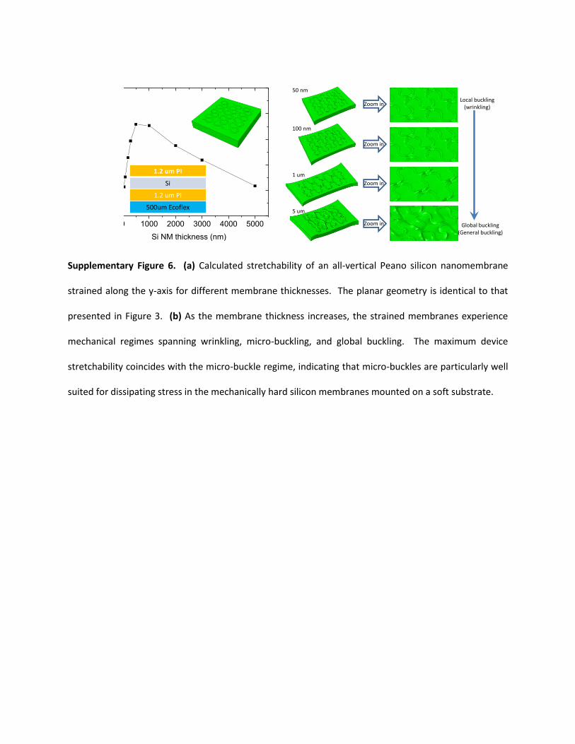
Supplementary Figure 6. (a) Calculated stretchability of an all-vertical Peano silicon nanomembrane
strained along the y-axis for different membrane thicknesses. The planar geometry is identical to that
presented in Figure 3. (b) As the membrane thickness increases, the strained membranes experience
mechanical regimes spanning wrinkling, micro-buckling, and global buckling. The maximum device
stretchability coincides with the micro-buckle regime, indicating that micro-buckles are particularly well
suited for dissipating stress in the mechanically hard silicon membranes mounted on a soft substrate.
100 nm
1 um
5 um
Zoom in
Local buckling(wrinkling)
Global buckling(General buckling)
50 nm
0 1000 2000 3000 4000 50000
20
40
60
80
100
S
tre
tch
ab
ility
(%
)
Si NM thickness (nm)
1.2 um PI
Si
1.2 um PI
500um Ecoflex
Zoom in
Zoom in
Zoom in

Supplementary Figure 7. (a) Optical image of a skin-mounted third order Peano temperature sensor.
Simultaneous measurements of temperature on skin with an infrared camera (b) show good agreement.
(c) A third order Peano device functions as a heater by passing larger amounts of current (order of
10mA) through the gold wires. The heat distribution within the device is uniform with and without
stretching due to the space filling properties of the wire layout.
98 mw
20%
stretching0%
stretching
2mm
a
Te
mpera
ture
( C
)
34.5
36
37.5
Time (sec)0 5010 20 30 40
IR camera
Fractal
b
Mounting on Forearm
c

Supplementary Figure 8. (a) The first order structure is a cross. Higher order structures are iteratively
constructed by adding crosses of exponentially smaller dimension, as shown. (b) For the electrodes
featured here, the connectivity between the structures (red lines) is defined such that there are no
closed loops of wire in the network. (c) The straight lines in the mathematical structure are replaced
with serpentine layout to enable stretchability.
b c
a

Supplementary Figure 9. A comparison of EMG signals taken from (a) fractal epidermal electrodes and
(b) gel-based electrodes mounted on the forearm show comparable signal-to-noise ratios. The peaks
are due to the clenching of the fist.
a b

Supplementary Figure 10. Illustration of the first three iterations of the Vicsek fractal.

Supplementary Figure 11. (a) Box fractal antenna geometry as imported in HFSS. The feed point of the
antenna is chosen so that the impedance of its fundamental mode sufficiently matches with the coaxial
feed. (b) Return loss spectra of the box fractal antenna for three different levels of stretching. It is
noted that the bandwidth of the box fractal is very narrow, due to the large inductive load built into the
antenna. (c) Far field intensity profile of the unstretched antenna at resonance.
1.4 1.8 2.2-40
-30
-20
-10
0
S1
1
Frequency (GHz)
0% stretching
10% stretching
20% stretching
a b c

Supplementary Table 1. Simulated uniaxial elastic stretchability for serpentine wires as a function of arc
solid angle. The inset in the middle column defines the arc solid angle. The cross- sectional geometries
and materials match those from Figure 3, and all structures have R = 620 µm and w = 70 µm (defined in
Supplementary Figure 2). These simulations clearly display that elastic stretchability increases as a
function of arc angle in these primitive serpentine geometries. As such, deterministically defining the
arc section geometries in wire-type structures can help optimize the mechanics.
Serpentine PatternsArc Angle
Elastic Stretchability
270° 61%
235° 60%
180° 36%
135° 18%
90° 6%

Supplementary Table 2. Simulated biaxial stretchability as a function of unit cell size for half-and-half
Peano structures. The cross- sectional geometries and materials match those from Figure 3, and all
structures have w = 70 µm (defined in Supplementary Figure 2). The structures with unit cell sizes
between 1.5 mm and 4.5 mm display biaxial stretchabilities greater than 20% and are compatible with
the elastic properties of skin23.
16% 28% 24% 23% 20%
6.0 mm 4.5 mm 3.0 mm 2.3 mm 1.5 mm

Supplementary Note 1: Analysis of Fractal Geometries with MicroXCT
Micro X-ray tomography (MicroXCT 400, Xradia) enables the imaging of the spatial topology of the
various fractal structures. Experimental images in Figures 1 and 3 demonstrate the structural details of
fractal patterns from the MicroXCT system. Two magnifications, 0.5 X and 4 X, provide the whole views
and magnified views of the structures, respectively. Additional imaging parameters include a 40 KeV X-
ray source and 200 µA current, with 600 image frames recorded stepwise over 180 degrees. TXM
Reconstructor software (Xradia) reconstruct the images, and the visualization software package (Amira
5.4.2, Visage Imaging) yields the “gray-scale” images in Figures 1 and 3.
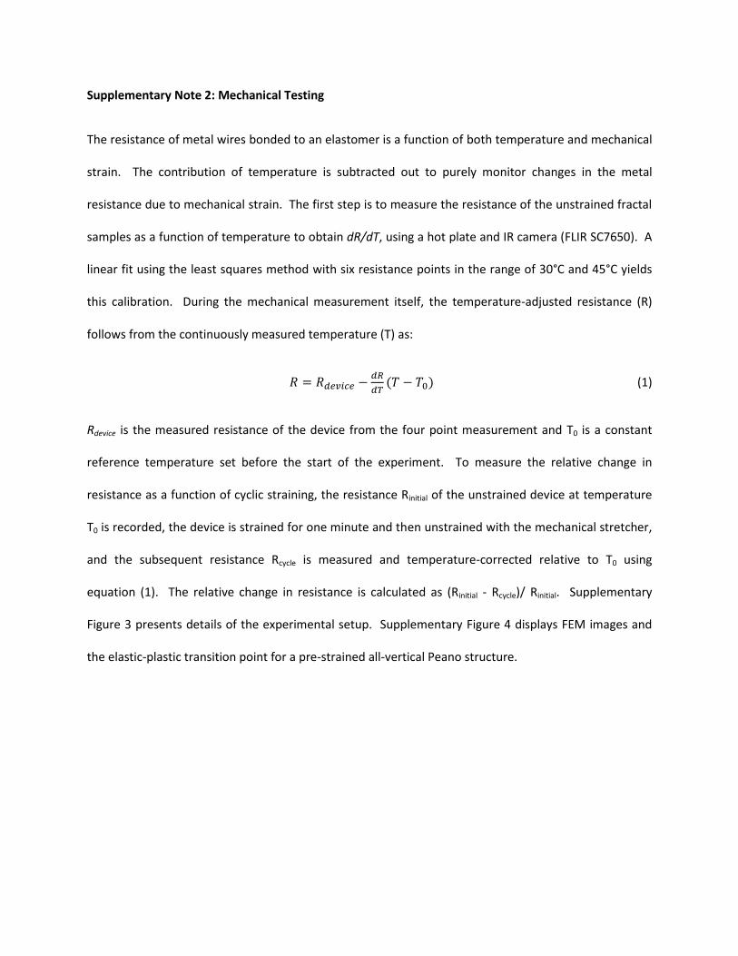
Supplementary Note 2: Mechanical Testing
The resistance of metal wires bonded to an elastomer is a function of both temperature and mechanical
strain. The contribution of temperature is subtracted out to purely monitor changes in the metal
resistance due to mechanical strain. The first step is to measure the resistance of the unstrained fractal
samples as a function of temperature to obtain dR/dT, using a hot plate and IR camera (FLIR SC7650). A
linear fit using the least squares method with six resistance points in the range of 30°C and 45°C yields
this calibration. During the mechanical measurement itself, the temperature-adjusted resistance (R)
follows from the continuously measured temperature (T) as:
(1)
Rdevice is the measured resistance of the device from the four point measurement and T0 is a constant
reference temperature set before the start of the experiment. To measure the relative change in
resistance as a function of cyclic straining, the resistance Rinitial of the unstrained device at temperature
T0 is recorded, the device is strained for one minute and then unstrained with the mechanical stretcher,
and the subsequent resistance Rcycle is measured and temperature-corrected relative to T0 using
equation (1). The relative change in resistance is calculated as (Rinitial - Rcycle)/ Rinitial. Supplementary
Figure 3 presents details of the experimental setup. Supplementary Figure 4 displays FEM images and
the elastic-plastic transition point for a pre-strained all-vertical Peano structure.

Supplementary Note 3: Temperature Sensor and Microheater Testing
Wires with Peano-based layouts have utility as the principal component in high-precision temperature
sensors and heaters. Such sensors can be calibrated against an infrared (IR) camera (A655SC, FLIR, USA),
as performed above for mechanical testing. The response of a third order half-and-half Peano sensor is
plotted in Supplementary Figure 7. The noise of the analogue-digital (A/D) converter ( ) and the
electrical noise ( ) determine the precision of the fractal temperature sensor using the expressions:
(
)
(1)
(
)
(2)
where dV/dT is from the temperature calibration. The precision of the fractal temperature sensor is
0.022 °C. Mounting a device on a forearm and recording the temperature simultaneously with the
sensor and an IR camera illustrates applicability to measurements on the skin.
The same device can be used as a precision element for Joule heating. Infrared images of a device under
0% and 20% uniaxial strain show that the heating is uniform across the area of the device, which is
indicative of the space-filling nature of the fractal construct (Supplementary Figure 7c). One application
involves wound recovery, for which the delivery of a controlled amount of heat to the wound vicinity
leads to increased local blood flow and vasodilatation and ultimately expedited recovery. The ability for
these devices to function as both temperature sensors and heaters enables the measurement of other
quantities, such as thermal conductivity.

Supplementary Note 4: Fractal Antenna Design and Simulations
The box fractal antenna layout utilizes the two dimensional box fractal illustrated in Supplementary
Figure 10. Here, five versions of the (N-1)th geometry scale down and connect together to construct the
Nth iterative geometry. A wire tracing around the perimeter of the box fractal creates the antenna
layout; the sharp corners are rounded to enhance the mechanics. The deformed antenna analysis with
HFSS simulations requires three steps: the undeformed antenna geometries import into Abacus, they
numerically stretch with a predetermined strain, and this resulting geometry imports into HFSS for
simulation (Supplementary Figure 11). The frequencies and magnitudes of the calculated S11
parameters, and the dipolar far field profiles, are consistent with those measured experimentally.

Supplementary Note 5: MRI Imaging
The spin echo images use the following parameters:
TR 2000
TE 25
Averages 5
Slices 25
FOV 140 x 140 mm
Thickness: 3 mm
Flip angle: 60 deg
Resol: 256
Partial fourier: 5/8
Bandwidth: 130 Hz/Px