Embed Size (px)
Citation preview

First principles simulations of
electron transport at the
molecule-solid interface
Hao Ren
School of Biotechnology
Royal Institute of Technology
Stockholm 2010

c⃝ Hao Ren, 2010
ISBN 978-91-7415-629-4
ISSN 1654-2312
TRITA-BIO-Report 2010:8
Printed by Universitetsservice US-AB,
Stockholm, Sweden, 2010

To my wife Xuan and to my parents.

iv

Abstract
In this thesis I concentrate on the description of electron transport properties of
microscopic objects, including molecular junctions and nano junctions, in partic-
ular, inelastic electron tunneling in surface-adsorbate systems are examined with
more contemplations. Boosted by the rapid advance in experimental techniques
at the microscopic scale, various electric experiments and measurements sprung
up in the last decade. Electric devices, such as transistors, switches, wires, etc.
are expected to be integrated into circuit and performing like traditional semi-
conductor integrated circuit (IC). On the other hand, detailed information about
transport properties also provides new physical observable quantities to charac-
terize the systems. For molecular electronics, which is in the state of growing up,
its further applications demands more thorough understanding of the underlying
mechanism, for instance, the effects of molecular configuration and conformation,
inter- or intra-molecular interactions, molecular-substrate interactions, and so on.
Inelastic electron tunneling spectroscopy (IETS), which reflects vibration features
of the system, is also a finger print property, and can thus be employed to afford the
responsibility of single molecular identification with the help of other experimental
techniques and theoretical simulations.
There are two parts of work presented in this thesis, the first one is devoted to
the calculation of electron transport properties of molecular or nano junctions: we
have designed a negative differential resistance (NDR) device based on graphene
nanoribbons (GNRs), where the latter is a star material in scientific committee
since its birth; The transport properties of DNA base-pair junctions are also exam-
ined by theoretical calculation, relevant experimental results on DNA sequencing
have been explained and detailed issues are suggested. The second part focused on
the simulation of scanning tunneling microscope mediated IETS (STM-IETS). We
have implemented a numerical scheme to calculate the inelastic tunneling intensity
based on Tersoff-Hamann approximation and finite difference method, benchmark
results agree well with experimental and previous theoretical ones; Two applica-
tions of single molecular chemical identification are also presented following bench-
marking.
v

Preface
The work presented in this thesis has been carried out at the Department of The-
oretical Chemistry, School of Biotechnology, Royal Institute of Technology, Stock-
holm, Sweden and National Laboratory for Physical Sciences at the Microscale,
University of Science and Technology of China, Hefei, China.
List of papers included in the thesis
Paper I Graphene nanoribbons as a negative differential resistance device
Hao Ren, Qunxiang Li, Yi Luo, and Jinlong Yang
Appl. Phys. Lett. 94, 173110(2009).
Paper II Important structural factors controlling the conductance of DNA pairs
in molecular junctions
Xiaofei Li, Hao Ren, Ling-Ling Wang, Ke-Qiu Chen, Jinlong Yang, and Yi Luo
J. Phys. Chem. C, submitted.
Paper III Simulation of inelastic electronic tunneling spectra of adsorbates from
first principles
Hao Ren, Jinlong Yang, and Yi Luo
J. Chem. Phys. 130, 134707(2009).
Paper IV Identifying configuration and orientation of adsorbed molecules by
inelastic electron tunneling spectra
Hao Ren, Jinlong Yang, and Yi Luo
J. Chem. Phys., submitted.
Paper V Determining tautomer structures of a melamine molecule adsorbed on
Cu(001) by inelastic electron tunneling spectroscopy
Shuan Pan, Hao Ren, Aidi Zhao, Bing Wang, Yi Luo, Jinlong Yang, and J. G.
Hou
in manuscript.
List of papers not included in the thesis

Paper I Quantum dot based on Z-shaped graphene nanoribbon: First-principles
study
Hao Ren, Qunxiang Li, Qinwei Shi, and Jinlong Yang, Chin. J. Chem. Phys. 20,
489(2007).
Paper II Edge effects on the electronic structures of chemically modified arm-
chair graphene nanoribbons
Hao Ren, Qunxiang Li, Haibin Su, Qinwei Shi, and Jinlong Yang
arXiv:0711.1700 [Cond-mat.matrl-sci](2007).
Paper III Strain effect on electronic structures of graphene nanoribbons: a first-
principles study
Lian Sun, Qunxiang Li, Hao Ren, Haibin Su, Qinwei Shi, and Jinlong Yang
J. Chem. Phys. 129, 074704(2009).
Paper IV Switching mechanism of photochromic diarylethene derivatives molec-
ular junctions
Jing Huang, Qunxiang Li, Hao Ren, Haibin Su, Qinwei Shi, and Jinlong Yang
J. Chem. Phys. 127, 094705(2007).
Paper V Single quintuple bond [PhCrCrPh] molecule as a possible molecular
switch
Jing Huang, Qunxiang Li, Hao Ren, Haibin Su, and Jinlong Yang
J. Chem. Phys. 125, 184713(2006).
Paper VI Theoretical study on the CF3CH3 + OH reaction
Huanjie Wang, Hao Ren, Dacheng Feng, and Yueshu Gu
Chem. J. Chin. Univ. 26, 1682(2005).
Paper VII Tunneling the electronic structures of graphene nanoribbons through
chemical edge modification: A theoretical study
Zhengfei Wang, Qunxiang Li, Huaixiu Zheng, Hao Ren, Haibing Su, Qinwei Shi,
and Jie Chen
Phys. Rev. B 75, 113406(2007).
vii

Comments on my contribution to the papers included
• I was responsible for the ideas, calculation and writing of the manuscripts of
paper I and IV;
• I was responsible for the formula derivation, calculation and writing of the
manuscript of paper III;
• I was responsible for part of the calculations and assist in the writing of the
manuscript of paper II;
• In paper V, I was responsible for the theoretical modeling and analysis, I
also assisted the writing of the manuscript.
viii

Acknowledgments
It is a pleasure to have this chance to express my gratitude and appreciation to
the people who helped me.
My supervisor Prof. Yi Luo played the most important role in the shaping of this
thesis. It was three years ago Prof. Luo gave me the chance to study in Sweden
and hold me from then on. I appreciate Prof. Luo introduced me a more fruitful
work style and his constant encouragement and enthusiasm. His breezy, optimistic
and surefooted attitude impressed me a lot and will affect me in my future life.
I would like to thank my supervisor in China, Prof. Jinlong Yang in University
of Science and Technology of China (USTC). He opened me a window to the
exciting academic life and provided the chance to study in Stockholm. His superior
knowledge, discerning intuition, rigorous attitude, and wide spectrum of research
interests set me an example that I intend following.
I would also like to thank Prof. Qunxiang Li in USTC, who accelerated my pace
to the fantasying field of nano-science and technology. My gratitude to Profs.
Dacheng Feng, Chengbu Liu, and Dongju Zhang in Shandong Unversity, China,
for their guidance when I was a undergraduate. Also thank Prof Haibin Su in
Nanyang Technological University, Singapore, for his guidance and encouragement.
Dr. Jun Jiang, Dr. Hongjun Xiang (USTC) and Dr. Bin Li (USTC) helped me a
lot in the early stage of implementation of our code. Great importance should also
be addressed of which fruitful discussions in experimental details and techniques
with Prof. Bing Wang (USTC) and Dr. Shuan Pan (USTC).
Frequently occurred discussions with Drs. Wenhua Zhang, Erjun Kan, Zhenpeng
Hu, Shuanglin Hu, Mrs. Keyan Lian, Misters Qiang Fu, Xiaofei Li, Ying Zhang, Sai
Duan, Weijie Hua, Guangjun Tian occasionally inspire me new ideas and enjoyed
me a lot. Lili Lin and Xin Li (DLUST) assisted me to prepare some figures of this
thesis.
Thanks to Drs. Zhenyu Li, Lanfeng Yuan, Xiaojun Wu, and Jing Huang for their
guidance and help.
The active and dynamic environment in Dept. of Theoretical Chemistry is exciting
and lead to high efficiency and happy working. I really appreciate the head of our
department — Prof. Hans Agren, and I’m sincerely thanks to all the people in the
department.
Thanks to the countless guys we live together in the last three years, without whom
I can not imagine the complete of the present thesis and how I can tide over the
ix

lonely days. I am glad to give my thanks to all of them: Bin Gao, Hui Cao, Kai
Fu, Na Lin, Tiantian Han, Kai Liu, Feng Zhang, Jicai Liu, Shilu Chen, Yuejie Ai,
Qiong Zhang, Zhijun Ning, Xing Chen, Xiao Cheng, Yuping Sun, Xiuneng Song,
Xin Li (ECUST), Fuming Ying, Jiayuan Qi, Zhihui Chen, Ke Zhao, Qun Zhang,
Ke Lin, Chunze Yuan, Qiu Fang, and many other friends in our group. Also thanks
to all the members in Prof. Yang’s group in USTC.
Thanks to China Scholarship Council (CSC) for the two years’ financial support
during 2007-2009.
Finally, my gratitude to my wife Xuan for her sweet love, unconditional under-
standing and support, immense patience; And to my parents, for their sincerely,
warmest and totally paying out.
x

Contents
1 Introduction 1
2 Electronic Structure Methods 5
2.1 Quantum theory and electronic structure . . . . . . . . . . . . . . . 5
2.2 Approximations . . . . . . . . . . . . . . . . . . . . . . . . . . . . . 7
2.2.1 Non-relativity approximation . . . . . . . . . . . . . . . . . 7
2.2.2 Born-Oppenheimer Approximation . . . . . . . . . . . . . . 7
2.2.3 Independent-electron approximation . . . . . . . . . . . . . 8
2.3 Hartree-Fock approximation and self-consistent method . . . . . . . 9
2.4 Density functional theory . . . . . . . . . . . . . . . . . . . . . . . . 10
2.4.1 Thomas-Fermi-Dirac Approximation . . . . . . . . . . . . . 11
2.4.2 Hohenberg-Kohn Theorem . . . . . . . . . . . . . . . . . . . 11
2.4.3 Kohn-Sham equation . . . . . . . . . . . . . . . . . . . . . . 12
2.4.4 Exchange-Correlation functionals . . . . . . . . . . . . . . . 14
2.5 Non-equilibrium Green’s function . . . . . . . . . . . . . . . . . . . 15
2.5.1 System and models . . . . . . . . . . . . . . . . . . . . . . . 15
2.5.2 Current Calculation . . . . . . . . . . . . . . . . . . . . . . . 17
3 Nano and Moleculear Electronics 19
3.1 Progress in molecular electronics . . . . . . . . . . . . . . . . . . . . 20
3.2 Experimental techniques . . . . . . . . . . . . . . . . . . . . . . . . 22
3.2.1 Scanning tunneling techniques . . . . . . . . . . . . . . . . . 22
3.2.2 Molecular junctions . . . . . . . . . . . . . . . . . . . . . . . 24
xi

CONTENTS
4 Graphene related materials 27
4.1 Geometric and electronic structures of graphene . . . . . . . . . . . 27
4.2 Preparation and characterization . . . . . . . . . . . . . . . . . . . 30
4.2.1 Physical approaches . . . . . . . . . . . . . . . . . . . . . . 31
4.2.2 Chemical approaches . . . . . . . . . . . . . . . . . . . . . . 31
4.2.3 Characterization of graphene . . . . . . . . . . . . . . . . . . 33
4.3 Graphene nanoribbons . . . . . . . . . . . . . . . . . . . . . . . . . 34
4.3.1 Fabrication of GNRs . . . . . . . . . . . . . . . . . . . . . . 34
4.3.2 Structural and electronic properties of GNRs . . . . . . . . . 35
5 Inelastic Electron Tunneling in Surface-Adsorbate Systems 39
5.1 Surface science and STM . . . . . . . . . . . . . . . . . . . . . . . . 39
5.2 STM mediated inelastic tunneling spectra . . . . . . . . . . . . . . 41
5.3 Simulation of STM-IETS . . . . . . . . . . . . . . . . . . . . . . . . 42
5.3.1 Calculation of Tunneling Current . . . . . . . . . . . . . . . 43
5.3.2 Inelastic electron tunneling . . . . . . . . . . . . . . . . . . . 44
6 Summary of papers 49
6.1 Molecular electronics . . . . . . . . . . . . . . . . . . . . . . . . . . 49
6.1.1 AGNR as a NDR device . . . . . . . . . . . . . . . . . . . . 49
6.1.2 Structural factors controlling the conductance of DNA pairs
junctions . . . . . . . . . . . . . . . . . . . . . . . . . . . . . 50
6.2 Inelastic tunneling spectra . . . . . . . . . . . . . . . . . . . . . . . 51
6.2.1 Method implementation and benchmarks . . . . . . . . . . . 51
6.2.2 Identifying adsorption configuration and orientation of cis-
2-butene adsorbed on Pd(110) surface . . . . . . . . . . . . . 53
6.2.3 Melamine tautomers adsorbed on Cu(100) surface . . . . . . 54
References 57
xii

1
Introduction
野马也,尘埃也,生物之以息相吹也;天之苍苍,其正色邪?其远而无
所至极也。
Zhuang-Zi(《庄子·逍遥游》, ∼ 369 B.C. — 286 B.C.)
Human’s cognition of nature evolves with the developments in science and tech-
nology. Probably the most familiar examples to the nowadays people are the
revolutions at the beginning of the last century that gave birth to the new physics:
relativity and quantum mechanics. It is commonly accepted that quantum the-
ory is suitable to describe microscopic processes occur in atoms, molecules or the
so-called nano-scale objects with dimensions from few angstroms to hundreds of
nanometers. The more interesting is, even in such a narrow area, starkly contrasted
viewpoints appears from time to time. In the early 1950s, Erwin Schrodinger be-
lieved that it is not possible to perform experiments to manipulate microscopic
particles such as electrons, atoms, or molecules [1]. However, only seven year lat-
ter, in 1959, Richard Feynman made his famous speech “There’s Plenty of Room
at the Bottom” [2], where he claimed that there is no physical principles that
restrict such microscopic manipulations, and different laws, different phenomena,
and different applications were expected in the virtue of pronounced quantum ef-
fects introduced by the small sizes. In fact, many of the phenomena Feynman
mentioned have been realized and are well known. For instance, high resolution
microscopes and minimized electric devices are not at all surprising and are playing
important roles in the daily life.
In order to reveal the underlying physics and chemistry of the emerging new phe-
nomena, theoretical investigations are inevitable and with great importance. On
the other hand side, just as described in the above paragraph, both predictions
1

1 Introduction
proposed from a theoretical point of view and theoretical studies will still play an
important role in the future evolution of science and technology.
As the most appropriate theory framework to describe atomic-scale objects and
phenomena [3], quantum theory has been the primary tools in the theoretical in-
vestigation of atoms, molecules and condensed matter. Atoms, consist of nuclei
and electrons, are the fundamental particles in chemistry, determines the prop-
erties of substance. Both the dynamics of nuclei and electrons can be described
by quantum theory, and in this context, the physical and chemical properties of
molecules, solids or even more complicated systems can be explained or predicted
in terms of quantum theory, at least in principle.
There seems a beautiful future when quantum mechanics is applied in the de-
scription of microscopic systems. Just as the famous proposition by P. A. M.
Dirac eighty years ago, that we had got almost all the desired rules to describe
the world, and the only questions left were the complexity of equations and the
lack of adequate mathematical skills to solve them [4]. The optimistic estima-
tion continued many years, much effort has been devoted into the development of
mathematical skills and numerical methods, such as the self-consistent field (SCF)
method [5], density functional theory (DFT) [6], quantum Monte Carlo methods
[7], and so on. However, the equations are so complex due to the so many degrees
of freedom. As a consequence, there is no exact analytic solutions for almost all
the systems encountered in practice except extremely simple systems.
Just as described in the quotation at the beginning of this chapter, all the living
and non-living objects in the world are interacting with each other by some kind
of breath, in such a manner, the sky is blue. Yet is blue the true color of the sky?
It is so far that beyond human’s scope. The key problem of electronic structure
theory is how to take into account of electron correlations, which appears when
more than one electron exists. The number of electrons in normal condensed
systems concerned is usually has the order of magnitude of 1023, in this context, the
only practical approach is to calculate the properties approximately, by employing
various approximations to models with accessible dimensions reduced by means of
consideration of symmetry, sacrifice of precision of less important part, etc.
Dissenting opinion to the reductionist hypothesis that everything can be reduced
to the few set of fundamental laws, however, was proposed by P. W. Anderson,
who believes that there would be new properties at each level of complexity, and
research of new rules under which new behaviors appear is also required [8]. Thus
in this constructionist context, chemistry is such a discipline obey the laws of many-
body physics, and the theoretical aspect of chemistry mainly concerns many-body
problem and its expression in systems consist of atoms, molecules and condensed
2

matter.
In this thesis, I will concentrate on the electronic structure theory and its applica-
tions at molecule-surface interfaces, both the electronic and transport properties of
such systems are investigated by using state-of-the-art simulation methods based
on electronic structure theory.
One of my topics is the simulation of electronic transport in molecular electronics.
Molecular electronics can be attributed to a growing point of Feynman’s speech
[2], and the first theoretical prediction is made by Aviram and Ratner, in 1974 [9],
where the authors proposed specific electric characteristics could be achieved by
constructing specific molecular devices and integrate into electric circuits. Thanks
to the advances in microscopic technologies such as scanning probe microscopy
[10, 11], molecule junction technique [12–14], people were able to construct such
devices at single molecular level in the recent years. Corresponding theoretical
simulation is desired in the further development of the new area, aimed to un-
derstanding of new behaviors observed in experiments, to gathering up new rules
from practical work, to predicting new phenomena would appear in specific sys-
tems, and to designing new devices. At present, the most widely used simula-
tion method in molecular electronics is non-equilibrium Green’s function (NEGF)
technique combined with DFT, several simulation schemes have been implemented
[15–21] and contributed a lot to the advance of this area. By employing the NEGF-
DFT scheme, we designed a negative differential resistance (NDR) device based
on graphene nanoribbons (GNRs), which exhibit robust NDR characteristics for
various systems with different sizes. We also re-examined an experimental work
devoted to DNA sequencing [22, 23], in which different DNA base pairs can be
identified by measuring their difference in conductance due to different number
of hydrogen bonds in the junctions. By performing first principles calculations,
we approved the possibility of such a electric approach to sequencing DNA pairs,
although the measurements in experiments was not exact enough to do so.
The other topic is devoted to the simulation of inelastic electron tunneling spec-
tra (IETS) in surface-adsorbate systems. IETS reflects the vibration features of
system, new tunneling channels would be opened when the injecting energy of
electrons is large enough to excite corresponding vibration mode. Usually these
inelastic contribution is considered to be small compared with its elastic coun-
terpart, and is omitted in many current or conductance oriented measurements.
However, IET would prominent in the quadratic differential of current respect to
voltage (d2I/dV 2), which can be directly measured or calculated numerically from
current-voltage characteristics. Due to its vibrational nature, IETS is a finger
print properties of the system, thus is powerful in the characterization of chemical
3

1 Introduction
species, geometry configuration or conformation, inter- or intra-molecular inter-
actions, molecule-surface interactions, and so on. Experimentally, IETS measure-
ment could be carried out by using molecular junction techniques or scanning tun-
neling technique. We implemented a scheme based on the finite difference method
proposed by Lorente and Persson [24, 25] to simulate IETS in surface-adsorbate
systems at first-principles level, the scheme is employed combined with the latest
experimental work, chemical identifications at single molecular level is achieved.
4

2
Electronic Structure Methods
The biggest difficulty in the modern electronic structure theory is to find an ap-
propriate approach to describe electron correlation interaction. In this point of
view, the developing of first principles calculation can be regarded as a journey
for further approximation about electron correlation along with the improvement
of calculation ability, for both hardware and software. Following this thread, in
this chapter, I briefly introduced the history of electronic structure theory and
first-principles calculations and then a concise description of Hartree-Fock approx-
imation and self-consistent method is presented, followed by a superficial depiction
of the widely used density functional theory and non-equilibrium Green’s function
method, where the later is employed in the calculation of electron transport prop-
erties in molecular devices.
2.1 Quantum theory and electronic structure
Most of the systems in practice we concerned are many-body systems, especially
for condensed matter systems, where the number of electrons possesses an order
of magnitude of Avogadro constant (NA ∼ 6.02×10²³). As a result of the massive
degrees of freedom, we should adopt a statistical physics point of view to handle
electronic structure problems. In 1925, W. Pauli proposed the famous exclusion
principle, which claimed it is not possible that two electrons occupy a same quan-
tum state simultaneously [26]. Exclusion principle could be further employed in the
explanation of the periodic table of chemical elements. Hereafter, E. Fermi gener-
alized Pauli’s exclusion principle into a statistical rule of non-interacting particles,
5

2 Electronic Structure Methods
e.g. Fermi-Dirac statistics:
fi =1
eβ(εi−µ) + 1(2.1)
where, fi is the occupation number of electrons on the i-th energy level, β = 1/kBT ,
relates to Boltzmann constant kB and temperature T , εi is the i-th eigenenergy,
µ is the chemical potential of system. Fermi-Dirac statistics and its counterpart
Bose-Einstein statistics are the fundamental rules for microscopic particles, corre-
sponding to fermions and bosons, respectively, and guarantee the wave functions
are antisymmetric or symmetric during exchanging two of N identical fermions or
bosons.
The procedure of simulating physical properties of system by using quantum me-
chanics is just the procedure of solving many-body Schrodinger equation of the
system. We must construct the Hamiltonian of the system first, for example, the
Hamiltonian of a typical many particle system can be written as the following
without any difficulty:
H = He +HI +HeI (2.2)
where
He =∑
i
pi2
2me
+∑
i<j
Vee(ri − rj)
HI =∑
I
pI2
2MI
+∑
I<J
VII(RI −RJ)
HeI =∑
iI
VeI(RI − ri)
(2.3)
here, ri and RI are the coordinates of the i-th electron and the I-th nucleus,
Vee, VII and VeI represent the interactions between electrons, nuclei and electron-
nucleus, respectively. Further consideration about other boundary conditions, such
as relativistic effects, spin, or electromagnetic filed, could be added as terms of
Hamiltonian.
Owing to the complexity of the problem, it is obvious that considering all the
degrees of freedom equally from an “ab-initio” manner is impossible. Thus various
approximations is necessary to reduce the calculation into a acceptable level.
6

2.2 Approximations
2.2 Approximations
The most rudimental approximations in quantum chemistry are non-relativity
approximation, Born-Oppenheimer approximation, and independent-electron ap-
proximation (Hartree approximation). These three approximations greatly reduced
the complexity of the problems we faced, thus forming the foundation of the whole
quantum chemistry. I will briefly describe these important ideas in the following.
2.2.1 Non-relativity approximation
As we all know that, the dynamics of massive body or objects with speed com-
parable with that of light could only be described properly in the framework of
relativity. In first principles calculations, thanks to the small mass of electrons and
most of the atoms, a non-relativity description should be exact enough. However,
consideration of relativistic effects is essential for heavy atoms, due to the high
speed of their core electrons [27].
There are several approaches to include relativistic effects into first-principles cal-
culation. For instance, relativistic effects can be directly included in the aug-
mentation method by using pure spin functions as basis[28–30], where these spin
functions are generated by solving relativistic radial equation. Or the relativis-
tic effects can be included in the building of pseudopotentials, during which the
relativistic Dirac equation is employed to carrying out atomic calculations, and
these relativistic pseudopotentials can be directly used to construct Hamiltonian
in following calculations[31, 32]. We use the pseudopotential approach to include
relativistic effects in our calculation if necessary in this thesis.
2.2.2 Born-Oppenheimer Approximation
Born-Oppenheimer approximation is also called adiabatic approximation. In the
Hamiltonian Eq. (2.3), there is only one term, of which the value is small enough
to be omitted in an accrual calculation: the kinetic energy term of nuclei∑
Ip2
I
2MI.
Compared with the mass of electrons, that of nuclei is immensely large. Even for
the lightest hydrogen atom, the ratio between the masses of nucleus and electron is
at the magnitude of order 103. Hence, we can approximate the masses of nuclei are
infinity, thus all the kinetic terms of nuclei can be omitted, then the Hamiltonian
can be written as:
H = T + Vext + Vint + EII (2.4)
7

2 Electronic Structure Methods
For simplicity, Hartree atomic unit is usually used in the deductions and calcula-
tions, where h = me = e = 4π/ϵ0 = 1. The terms in the above equation can thus
be expressed as: Kinetic energy T ,
T =∑
i
−1
2∇2
i , (2.5)
where ∇2 = ∂2
∂x2 + ∂2
∂y2 + ∂2
∂z2 is Laplace operator.
The external potential of electrons from nuclei Vext,
Vext =∑
i,I
VI(|ri −RI |) (2.6)
the Coulomb interactions among electrons Vint,
Vint =1
2
∑
i=j
1
|ri − rj|(2.7)
and the last term EII , represents the classical Coulomb interactions between nuclei,
is an constant for a specific configuration.
With the help of Born-Oppenheimer approximation, the number of degrees of free-
dom of the system is further reduced, all the contribution from nuclei interactions
is nothing but a constant.
2.2.3 Independent-electron approximation
In fact, the so-called independent-electron approximation can be classified as two
approaches [33], they are Hartree approximation and Hartree-Fock approximation,
where the latter takes into account the antisymmetric wave functions under ex-
changing particles for fermions systems. I will only describe Hartree approximation
in this section, and leave its further development in the next, combined with the
self-consistent method.
Hartree approximation was proposed in 1928, by D. R. Hartree [5], in which the
complex interactions among electrons can be approximated as a single electron
moving in an effective field composed by the other electrons and all the nuclei,
therefore, the many electron problem is simplified as a spherical potential system.
The inter-electron Coulomb interactions in Eq. (2.7) can be expressed as
Vint =∑
i
vHi (2.8)
where the Hartree potential vHi is the average potential that the i-th electron
experiences.
8

2.3 Hartree-Fock approximation and self-consistent method
2.3 Hartree-Fock approximation and self-consistent
method
There is no consideration of the antisymmetric nature of electron wave functions
in the original Hartree approximations [5]. In 1930, Fock used an antisymmetrized
determinant wave function to solve the time-independent Schrodinger equation
HeffΨσi (r) =
[− h2
2me
∇2 + V σeff (r)
]Ψσ
i (r) = ϵσi Ψσi (r) (2.9)
where V σeff (r) is the effective potential experienced by electron with spin σ at
position r. For N-electron system, the single Slater determinant can be written as
[34]:
Ψ =1
(N !)1/2
∣∣∣∣∣∣∣∣∣
ϕ1(r1, σ1) ϕ1(r2, σ2) ϕ1(r3, σ3) · · ·ϕ2(r1, σ1) ϕ2(r2, σ2) ϕ2(r3, σ3) · · ·ϕ3(r1, σ1) ϕ3(r2, σ2) ϕ3(r3, σ3) · · ·
......
.... . .
∣∣∣∣∣∣∣∣∣(2.10)
where ϕi(rj, σj) is the single-electron spin orbital, it’s the product of position
component ψi(ri) and spin component αi(σi).
According to the variational method, the ground state energy of system has the
following form [34, 35]:
E = ⟨Ψ|H|Ψ⟩ =∑
i,σ
∫drψσ∗
i (r)
[−1
2∇2 + Vext(r)
]ψσ
i (r) + EII
+1
2
∑
i,j,σi,σj
∫drdr′ψσi∗
i (r)ψσj∗j (r′)
1
|r− r′|ψσii (r)ψ
σj
j (r′)
− 1
2
∑
i,j,σ
∫drdr′ψσ∗
i (r)ψσ∗j (r′)
1
|r− r′|ψσj (r)ψσ
i (r′)
(2.11)
the first term in Eq (2.11) is single particle energy, the second and third terms
are Coulomb interaction and exchange interaction between electrons, respectively.
The Coulomb term is also called Hartree term:
EHartree =1
2
∫drdr′
n(r)n(r′)
|r− r′| (2.12)
where n(r) is the electron density at position r. Since the spin orbitals of different
spin degree of freedoms mutually orthogonal to each other, only exchange among
electrons with same spin contributes.
9

2 Electronic Structure Methods
Variate energy respect to all the variables, we then get the Hartree-Fock equation
−1
2∇2 + Vext(r) +
∑
j,σj
∫dr′ψ
σj∗j (r′)ψ
σj∗j (r′)
1
|r− r′|
ψσ
i (r)
−∑
j
∫dr′ψσ∗
j (r′)ψσi (r′)
1
|r− r′|ψσi (r) = ϵσi ψ
σi (r)
(2.13)
the above equation can be written into a single particle equation in the following
form:
Heffi ψi,σ(r) =
[−1
2∇2 + V eff
i,σ (r)
]ψi,σ(r) = ϵi,σψi,σ(r) (2.14)
It is obvious in Eq. (2.13) that each of the spin orbitals depend on the others,
hence Eq. (2.13) is a nonlinear equation and can only be solved by self-consistent
method. Indeed, the numerical method employed in solving Hartree-Fock equation
is named “self-consistent field” (SCF) method.
SCF method initializes with a set of guess spin orbitals and thus the Hamiltonian
can be constructed, by substituting into Hartree-Fock equation (2.13), a new set
of spin orbitals would be generated, from these new orbitals new Hamiltonian can
be constructed, and another new set of spin orbitals can be obtained, such loop
revolves until convergence is achieved.
Hartree-Fock approximation and SCF method are cornerstones of electronic struc-
ture calculations. It is difficult to bypass them in most of the modern calculation
approaches. However, there is no consideration of electron correlation in Hartree-
Fock approximation, which largely restrict its application in various areas. Electron
correlation amounts for about 1% of the system total energy, hence Hartree-Fock
is a good approximation for energy calculations. Whereas for many cases, such as
calculations of bond energy, excitation energy, barrier in chemical reactions, ad-
sorbe/desorbe energy etc., where the energy difference between different systems is
essential, Hartree-Fock can hardly provide a reasonable result. To resolve the cor-
relation nightmare, various methods have been proposed based on Hartree-Fock
method, such as configuration interaction (CI) [34], Møller-Plesset perturbation
method (MPn) [34, 36], and so on.
2.4 Density functional theory
The most intolerable defect of traditional quantum chemistry calculation method,
including Hartree-Fock and its further development — post Hartree-Fock (CI,
10

2.4 Density functional theory
MPn, etc.), is the tremendous calculational complexity. For example, O(N4) for
Hartree-Fock, O(N5) for MP2, and especially for full configuration interaction
method, the complexity exponential increases with the number of particles. Indeed,
the application of these methods is usually limited for systems with moderate
sizes. On the other hand, there is only one variable — electron density — in
density functional theory (DFT), where any physical quantity can be expressed as
a functional of electron density n(r). The calculational complexity of DFT is only
at the order of O(N2) ∼ O(N3).
2.4.1 Thomas-Fermi-Dirac Approximation
The original ideas of DFT were proposed by Thomas [37] and Fermi [38] in 1927,
where they expressed the kinetic energy term with a explicit functional of electron
density [33]. In 1930, Dirac took into account the local approximation of electron
exchange and correlation interactions, which was omitted in Thomas-Fermi ap-
proximation, derived Thomas-Fermi-Dirac approximation [39], where the energy
functional is expressed as:
ETF [n] =C1
∫drn(r)5/3 +
∫drVext(r)n(r)
+ C2
∫drn(r)4/3 +
1
2
∫drdr′
n(r)n(r′)
|r− r′|
(2.15)
where the first and third terms are the local approximation of electron kinetic
energy and exchange energy, respectively. The last term is classical Hartree energy.
Despite Thomas-Fermi-Dirac approximation proposed a heuristic method to han-
dle the degrees of freedom of many electron systems, its lack in detailed physical
and chemical information restricts its application in actual calculations.
2.4.2 Hohenberg-Kohn Theorem
It is commonly accepted that the two theorems proposed by Hohenberg and Kohn
in 1964 [6] are the onset of modern DFT. These two Hohenberg-Kohn (HK) the-
orems constituted the foundation of modern density functional theory, and I shall
retail them in the following [33, 40, 41]:
HK Theorem I: For any systems of N-interacting electrons, any of its physical
properties are completely determined by the ground state electron density n(r).
11

2 Electronic Structure Methods
HK Theorem II: The global minimum of energy functional is the ground state
energy, and the corresponding electron density is the ground state density.
We can write the Hamiltonian of any many-electron system as
H = −1
2
∑
i
∇2 +∑
i
Vext(r) +1
2
∑
i =j
1
|ri − rj|(2.16)
and the energy functional can be expressed as
EHK [n] = T [n] + Eint[n] +
∫drVext(r)n(r) + EII
= FHK [n] +
∫drVext(r)n(r) + EII
(2.17)
where EII is nucleus-nucleus interaction, FHK [n] is system internal energy, includ-
ing electron kinetic energy, potential energy and interaction energy.
2.4.3 Kohn-Sham equation
The HK theorems ensure that all the physical properties are determined by ground
state density on the premise of we have got the explicit energy functional of density.
However, it is so difficult that there is no such exact functional so far. In 1965,
Kohn and Sham proposed that the many-electron system can be replaced by a
fictitious non-interacting many particle system with the same external potential,
all the interactions between electrons are classified into a exchange-correlation
(XC) term. The ground state density and other properties can be obtained by
solving the non-interacting system, and the precision only depends on the quality
of XC functional.
We can write the Hamiltonian of the auxiliary fictitious system as
Hσaux = −1
2∇2 + Vσ(r) (2.18)
and the electron density
n(r) =∑
σ
n(r, σ) =∑
σ
Nσ∑
i=1
|ψσi (r)| (2.19)
where ψσi is the i-th single particle orbital with spin component σ. Thus the kinetic
term is
Ts = −1
2
∑
σ
Nσ∑
i=1
⟨ψσi (r)|∇2|ψσ
i (r)⟩ =1
2
∑
σ
Nσ∑
i=1
∫dr|∇ψσ
i (r)|2 (2.20)
12

2.4 Density functional theory
and the classical Coulomb term can defined as the interaction between electron
density with itself:
EHartree =1
2
∫drdr′
n(r)n(r′)
|r− r′| (2.21)
In this way, we can write out the energy functional as the following:
EKS = Ts[n] +
∫drVext(r)n(r) + EHartree[n] + EII + EXC [n] (2.22)
where all the many body effects are included in EXC term.
Subject to the orthonormal constraint of orbitals
⟨ψσi |ψσ′
j ⟩ = δi,jδσ,σ′ (2.23)
we have the variational equation of energy functional at ground state
δEKS
δψσ∗i (r)
=δTs
δψσ∗i (r)
+
[δEext
δn(r, σ)+δEHartree
δn(r, σ)+
δEXC
δn(r, σ)
]δn(r, σ)
δψσ∗i (r)
= 0 (2.24)
and then a Schrodinger-like equation
(HσKS − ϵσi )ψσ
i (r) = 0 (2.25)
is obtained, which is called Kohn-Sham (KS) equation, where ϵσi is the i-th eigenen-
ergy for spin σ, and KS effective Hamiltonian
HσKS(r) = −1
2∇2 + V σ
KS(r) (2.26)
here, V σKS is KS potential
V σKS(r) = Vext(r) +
δEHartree
δn(r, σ)+
δEXC
δn(r, σ)
= Vext(r) + VHartree(r) + V σXC(r)
(2.27)
Equations (2.25) – (2.27) are KS equations. It is obvious that we should have
resorts to SCF method to solve KS equations. Moreover, the KS scheme is inde-
pendent of the selection of exchange-correlation approximations.
The KS orbitals are usually described as linear combinations of a set of functions,
which is called basis set. The basis set should be infinite dimensional in principle,
which is evidently impossible to be implemented in practice. In most of the cases,
a cutoff is used to truncate the number of dimensions. There are many kinds
of basis set are widely used in calculations, such as Salter type orbitals (STO)
[42], Gaussian type orbitals (GTO) [43], plane waves [33], Wannier functions [44],
13

2 Electronic Structure Methods
wavelets [45], and so on. Among these kinds of basis sets, STO and GTO are
widely used in traditional quantum chemistry calculations, due to the ease to
describe atomic orbitals. On the other hand, plane wave basis is the most natural
way to do calculations under periodic conditions, and most of the widely used solid
state simulation packages adopt plane wave basis.
2.4.4 Exchange-Correlation functionals
KS scheme transforms the quantum many-electron problem into a effective single
electron problem, and dumps all the un-exact part into exchange-correlation term,
thus, a EX functional with high quality is essential for our calculation. Moreover,
the explicit separation of kinetic and Hartree term from the total energy implies
that the EX functional would be localized [33]. Despite the exact expression of
EX potentials should certainly be very complex, we still have some clews from
its various boundary conditions. Some kinds of widely used XC functionals are
present in the following.
local (spin) density approximations, L(S)DA
The exchange and correlation interactions is localized in homogenous electron gas,
thus the XC functional only depends on electron density [33, 41]
ELDAXC [n↑, n↓] =
∫drn(r)ϵhom
XC (n↑(r), n↓(r))
=
∫drn(r)
[ϵhomX (n↑(r), n↓(r)) + ϵhom
C (n↑(r), n↓(r))] (2.28)
LSDA performs very well in metallic system, as a result of most of the electron
states near Fermi energy are delocalized, thus is a good approximation to homoge-
nous electron gas.
Generalized gradient approximations, GGA
In addition to the dependence on electron density, GGA also takes into account of
the dependence on gradient of electron density [33, 41]
EGGAXC [n↑, n↓] =
∫drn(r)ϵXC(n↑(r), n↓(r), |∇n↑|, |∇n↓|, . . . )
=
∫drn(r)ϵhom
X (n)FXC(n↑(r), n↓(r), |∇n↑|, |∇n↓ |, . . . )(2.29)
14

2.5 Non-equilibrium Green’s function
where FXC is a dimensionless quantity, ϵhomX (n) is the exchange of non-polarized
homogenous electron gas.
GGA improves the performance in complex chemical environments, especially for
binding energy calculation of molecules and solids, where chemical precision is
achieved [40]. As a result, GGA greatly extended the application of DFT. There
are many GGA functionals so far, such as Becke88 [46], PW91 [47], PBE [48] etc.,
all these functionals are widely used in the nowadays calculations.
Hybridized functions
As we all know that the description of exchange interaction is exact in Hartree-
Fock method, if we take the exact exchange and linearly combined with exchange
or correlation taken from LSDA or GGA, the constructed new functional is called
hybridized exchange-correlation functional. Usually these functionals are better
approximations for specific systems [33, 40, 49].
2.5 Non-equilibrium Green’s function
First-principles calculation brought a reliable approach which is popularized and
applied in many areas in the recent decades [33, 41, 50–53]. However, traditional
first-principles methods also possesses its limitations, for example, only finite-sized
systems or infinite systems with internal periodicity can be calculated, in addition,
these systems must be in equilibrium. In this context, systems in molecular elec-
tronics, which are non-equilibrium, non-periodic, and infinite with open boundary
conditions could not be treated properly by using these traditional methods. The
good thing is creativeness never cower away when demands appear. In this sec-
tion, I would like to briefly describe the framework of non-equilibrium Green’s
function (NEGF) technique and how to calculate the electron transport properties
numerically by employing NEGF combined with DFT [54–57].
2.5.1 System and models
A typical open system in molecular electronics can be simplified into a model shown
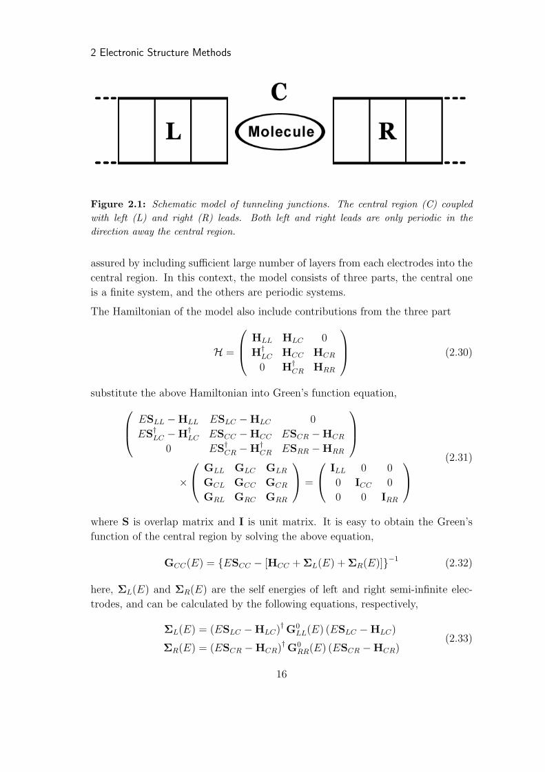
in Figure 2.1, where C, L and R represents the central region (usually constructed
by molecules), the left and right electrodes. Both the electrodes are semi-infinite
and extend periodically to left and right, respectively. It is commonly assumed
that there is no direct interaction between left and right electrodes, which can be
15
2 Electronic Structure Methods
Figure 2.1: Schematic model of tunneling junctions. The central region (C) coupledwith left (L) and right (R) leads. Both left and right leads are only periodic in thedirection away the central region.
assured by including sufficient large number of layers from each electrodes into the
central region. In this context, the model consists of three parts, the central one
is a finite system, and the others are periodic systems.
The Hamiltonian of the model also include contributions from the three part
H =
HLL HLC 0
H†LC HCC HCR
0 H†CR HRR
(2.30)
substitute the above Hamiltonian into Green’s function equation,
ESLL −HLL ESLC −HLC 0
ES†LC −H†
LC ESCC −HCC ESCR −HCR
0 ES†CR −H†
CR ESRR −HRR
×
GLL GLC GLR
GCL GCC GCR
GRL GRC GRR
=
ILL 0 0
0 ICC 0
0 0 IRR
(2.31)
where S is overlap matrix and I is unit matrix. It is easy to obtain the Green’s
function of the central region by solving the above equation,
GCC(E) = ESCC − [HCC + ΣL(E) + ΣR(E)]−1 (2.32)
here, ΣL(E) and ΣR(E) are the self energies of left and right semi-infinite elec-
trodes, and can be calculated by the following equations, respectively,
ΣL(E) = (ESLC −HLC)† G0LL(E) (ESLC −HLC)
ΣR(E) = (ESCR −HCR)† G0RR(E) (ESCR −HCR)
(2.33)
16
2.5 Non-equilibrium Green’s function
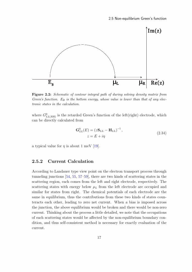
Figure 2.2: Schematic of contour integral path of during solving density matrix fromGreen’s function. EB is the bottom energy, whose value is lower than that of any elec-tronic states in the calculation.
where G0LL(RR) is the retarded Green’s function of the left(right) electrode, which
can be directly calculated from
G0LL(E) = (zSLL −HLL)−1 ,
z = E + iη(2.34)
a typical value for η is about 1 meV [19].
2.5.2 Current Calculation
According to Landauer type view point on the electron transport process through
tunneling junctions [54, 55, 57–59], there are two kinds of scattering states in the
scattering region, each comes from the left and right electrode, respectively. The
scattering states with energy below µL from the left electrode are occupied and
similar for states from right. The chemical potentials of each electrode are the
same in equilibrium, thus the contributions from these two kinds of states coun-
teracts each other, leading to zero net current. When a bias is imposed across
the junction, the above equilibrium would be broken and there would be non-zero
current. Thinking about the process a little detailed, we note that the occupations
of each scattering states would be affected by the non-equilibrium boundary con-
dition, and thus self-consistent method is necessary for exactly evaluation of the
current.
17

2 Electronic Structure Methods
Following Landauer’s type formula, the current under steady state approximation
is
I(Vb) = −2e2
h
∫ +∞
−∞T (E, Vb)[f(E − µL)− f(E − µR)]dE, (2.35)
where µL(R) is the chemical potential of left(right) electrode, f is Fermi-Dirac
distribution function, T (E, Vb) is the transmission probability of injecting electrons
with energy E when a bias Vb is imposed. Transmission function can be calculated
directly from the Green’s function of the scattering region
T (E, Vb) = Tr[ΓL(E)GCC(E)ΓR(E)G†CC(E)] (2.36)
Here, the self energy
ΓL(R)(E) = i(ΣL(R)(E)− [ΣL(R)(E)]†
)(2.37)
reflects the coupling between electrodes and central region at energy E.
The density matrix of the system can also relate to the Green’s function [18–20, 60]
DCC =1
2π
∫ +∞
−∞dE
[GCC(E)ΓL(E)G†
CC(E)f(E − µL)
+ GCC(E)ΓR(E)G†CC(E)f(E − µR)
]
=− 1
π
∫ +∞
−∞dEℑ [GCC(E)f(E − µL)]
+1
2π
∫ +∞
−∞dE
[GCC(E)ΓR(E)G†
CC(E)][f(E − µR)− f(E − µL)] .
(2.38)
the first term is analytical thus can be evaluated by using contour integral approach
(see Figure 2.2) with high efficiency. On the other hand, there exists singular points
in the second term, thus a dense mesh grid is necessary for the calculation.
The density matrix can be feed back to DFT modules to generate new ground
state density,
ρ(r) =∑
µ,ν
ϕ∗µ(r)ℜ [(DCC)µ,νϕν(r)] , (2.39)
and Hamiltonian
(HCC)µ,ν = ⟨µ|T + Vext(r) + VH [ρ(r)] + VXC [ρ(r)]|ν⟩, (2.40)
thus a new iteration starts from the calculation of new Green’s function, and
iterates until convergence is achieved. Then the current can be calculated by using
Eq. (2.36) and Eq. (2.35). For non-zero bias calculations, the above scheme can
be used followed by shifting the chemical potentials of left and right electrode by
eVb/2 upwards and downwards, respectively.
18

3
Nano and Moleculear Electronics
Despite the prediction of manipulating objects at atomic scale by Feynman is as
early as at the end of 1950s [2], the actual implementation is after 1982, when
Binnig and Rohrer invented scanning tunneling microscope (STM) in Zurich [10].
STM based on the quantum tunneling phenomena, and the first time supply a
practical approach to observe objects and processes at atomic scale. The pristine
STM use tunneling current or conductance as indication in the measurements,
thus it is necessary that the tunneling system is conductive, which restricts its
application in insulating or liquid phase systems. Four years latter, in 1986, Binnig
and coworkers invented atomic force microscope (AFM) [11], greatly expanded
the scope of scanning probe techniques. Besides, other spectroscopy [61–63] or
illuminating techniques [62, 64, 65], high resolution spectroscopic methods [66–
68] and nano-scale preparation and manufacture [12–14] etc. also boost the rapid
growth of this area.
The terminology nano-materials implies that materials with at least one of its
dimensions is at nanometer scale [69], for example, molecules and clusters are zero-
dimensional, nanotubes and nanowires are one-dimensional, few-layered graphene
and atomically thin bismuth telluride are two-dimensional. Nano-electronics is
the study of electric circuits composed by nano-materials, and in this context,
molecular electronics is just a special case of nano-electronics, where the circuits
consist of various molecules. Owing to the small sizes, especially for cases that one
of the system dimension is comparable with the characteristic length of microscopic
particles in it, we must seek help from quantum mechanics; On the other hand, the
ratio of surface atoms increases as the system size decreases. These two issues are
responsible for the new behaviors emerged, which are highly dependent on the size,
shape, chirality, composition etc. of the system. Furthermore, such dependencies
lead to versatile properties and thus provide potential applications in the future
19

3 Nano and Moleculear Electronics
Figure 3.1: A schematic view of Moore’s Law. The number of transistors in a singleprocessor and the manufacture process are presented as green and red curves, respectively.All the data take from the website of Intel R⃝corporation [71].
mechanics, electrics, magnetics, and chemistry [70].
3.1 Progress in molecular electronics
The size of electronic devices in silicon industry is approaching its physical limit in
the recent years, the revenue production of 32 nm products has begun and 22 nm
technologies is in development, and will appear on the market in middle 2010 [71].
According to Moore’s Law (though seems being invalidate recently, see Figure 3.1),
the number of transistors on unit area doubles every 18 months [72], the actual size
of a single transistor will down to atomic scale, and the traditional semiconductor
techniques will no longer work owing to two issues: Firstly, the resolution of light
etching technique will reach its limit due to the finite wave length; secondly, silicon
dioxide, the widely used insulating layer in traditional metal-oxide-semiconductor
field-effect transistor (MOSFET), would be conductive when its thickness down to
0.7 nm [16]. Seeking for new devices with smaller sizes, higher performance and
lower energy consumption becomes an urgent problem.
We usually trace back to Aviram and Ratner’s proposal of molecular rectifier [9]
as the origin of the concept of molecular electronics. In the work nearly 40 years
ago, the authors proposed that rectification can be implemented by a two probe
molecular junction in which the molecule consist of an acceptor-donor pair. This
kind of approaches to construct devices from single molecules or clusters are called
20

3.1 Progress in molecular electronics
“bottom-up” method, compared with the traditional “top-down” methods, molec-
ular devices would be much smaller and be much easier to tune their functions.
Molecular electronics became popular just in the latest twenty years, by the virtue
of the advancements in chemical synthesis and microscopic characterization. To
realize electronic chips at molecular level, the electron transport properties of single
molecules must be characterized at first. At present, most of the studies in this area
are in the early stage. As the result of the complexity and diversity of composition
and configuration of molecules, single molecular junctions exhibit versatile electric
characteristics, such as rectification [73–75], amplification [76], filed modulation
[77], giant magnetic resistance [78, 79], Coulomb blockage [80], Kondo effects [79–
81], and so on.
The advances in experimental techniques brought great challenges and opportuni-
ties to the theoretical aspect. In most of the experiments, the detailed configuration
and conformation of molecules under the influence of electrodes, the structure of
electrodes, or the effects of electrode-molecule interactions will strongly affect the
transport properties of the junctions. However, these factors could not be com-
pletely characterized so far. Identifying the correspondence between experimental
measurements and detailed compositional and structural information of the molec-
ular junction is indispensable for the further development of molecular electronics.
Theoretical simulation is the most effective approach to achieve this goal, not only
because of its high cost effective, we can also perform ideal experiments and design
molecular devices with specific electric functionalities.
Electron transport through molecular junctions is a non-equilibrium process with
open and non-periodic boundary conditions, thus new theoretical framework/method
is needed to describe these new behaviors. The first first-principles electron trans-
port calculation was carried out by Di Ventra and co-workers, where the authors
using muffin-tin model to describe the metal electrodes and employing Lippman-
Schwinger equation to calculate the conductance [15]. However, as a consequence
of the using of plane wave basis, the dimensions of matrices in the calculation is
tremendously large, which prevented its popularization in the simulation commu-
nity. Taylor et al. combined the non-equilibrium Green’s function technique and
density functional theory (NEGF-DFT) to calculate the conductance of molecular
junctions, localized atomic orbital basis set is used in the calculation, for its effi-
ciency [17, 18]. NEGF-DFT is the most popular approach for electron transport
calculation so far [16, 19, 20].
21

3 Nano and Moleculear Electronics
3.2 Experimental techniques
Because of the close contact of the works in this thesis with the experimental
developments, I shall briefly introduce some of the related experimental techniques
in this section.
3.2.1 Scanning tunneling techniques
For a long time, there are mainly two kinds of approaches to collect microscopic
structural information of materials. One is diffraction techniques which employing
the wave character of light or microscopic particles to diffract with the periodic
structure of material, information about the reciprocal lattice can be character-
ized. X-ray diffraction (XRD), X-ray photoelectron spectroscopy (XPS), low en-
ergy electron diffraction (LEED) etc. are some examples of these techniques, which
concentrate on the periodic information of materials. However, these techniques
are limited by the purity of light or particles and their inability in real space char-
acterization. The other one is high resolution microscopy that detects the local
structural information in real space, including high resolution optical microscopy,
scanning electron microscopy (SEM) [82], transmission electron microscopy (TEM)
[83], field ion microscopy (FIM) [84] and so on. The applicabilities of these methods
are also restricted by the wave length of light or particles.
The invention of STM, AFM and a series of other scanning probe microscopes
provide the possibility to detect local structural information in real space at the
mean time with an atomic resolution. The lateral and vertical resolution of STM is
about 1 A and 0.1 A, respectively [85, 86]. STM works with the quantum tunneling
principle, upon which electrons probably tunneling through a classically forbidden
barrier with energy higher than itself. A schematic view of STM is presented in
Figure 3.2, in which the sample adsorbed on conductive substrate plus the STM
tip constitute a circuit, and the vacuum region between tip and sample can be
viewed as the tunneling barrier. The probability of electrons tunneling between
tip and sample depends on the imposed bias voltage, the physical and chemical
properties of substrate, sample and STM tip.
Constant current mode and constant height mode are the commonest among the
scanning modes of STM [88]. In constant current mode, the tunneling current is
fixed and thus the tip height changes according to the change of density of states
(DOS), a topographic mapping of the sample DOS is obtained after scanning;
Whereas in constant height mode, the tip height and bias voltage are fixed and
the scanned map reflects the spatial distribution of sample DOS in the cross plane
22

3.2 Experimental techniques
Figure 3.2: Schematic drawing of STM. Created by Michael Schmid, TU, Wein. Alsoavailable at Wikimedia commons [87].
on which tip moves. Besides, scanning tunneling spectroscopy (STS) is often used
in measurement, in which the tip position is fixed and the bias voltage gradually
changes, by recording the change in current, a current-voltage curve is obtained. In
a STM measurement, a typical bias voltage is about 0.1 V and a typical tunneling
current is about 1 nA, usually the vacuum barrier is about 5 ∼ 7 A in length [88].
In most of the cases, the measured tunneling current and STM images depend on
the geometrical configuration and electronic structures of the sample, the STM tip
can also effect experimental results [86, 89].
Abundant information about the electronic states of the sample, especially local
properties can be obtained by numerous repeatable STS measurements, where the
current-voltage (I-V), differential I-V (dI/dV ), and quadratic differential (d2I/dV 2)
characteristics reflect the distribution of electronic and vibrational states in energy
space. Due to these properties strongly dependent on the chemical composition,
geometry configuration and conformation, sample-substrate interaction, and intra-
or inter-molecular interactions (if any), STM is capable of detailed characterizing
the sample-substrate systems.
The contributions to tunneling conductance can be classified as elastic and in-
elastic part, elastic tunneling usually dominate the tunneling process, in which
electrons experience elastic scattering and their energy conserves. The resonant
tunneling model can be used to describe elastic tunneling processes: The Fermi
levels of electrodes shift in opposite direction when a bias V is imposed, hence
there would be a energy window with width eV . If there are delocalized states
23

3 Nano and Moleculear Electronics
in the junction with energy in the range covered by the energy window, electrons
with corresponding energy in the electrode would tunneling through the junction
to the unoccupied states at the other side. In this context, tunneling current
and thus conductance appear, and the delocalized states in the junction is called
tunneling channel that provides a pathway for the injected electrons [54, 55, 57].
The requirement of electrons experience elastic tunneling delimits that tunneling
occurs only there exists occupied and empty states with energy matches tunneling
channels. This is only a simplified description of the actual tunneling process, in
which various other factors effects. The most obvious is the inelastic scattering
between tunneling electrons and vibration modes (phonons) of the sample, where
injecting electrons exchange energy with the vibration modes of nuclei. Inelastic
tunneling occurs when the injecting electrons possess large enough energy to ex-
cite a specific vibration mode, thus it can be viewed as a new tunneling channel
is opened by inelastic electron excitation. The inelastic contributions lead to a
suddenly change in tunneling conductance, and can be characterized by the peaks
in differential conductance (d2I/dV 2) spectrum, which is called inelastic electron
tunneling spectra (IETS), and is a powerful tool in microscopic characterization. In
addition, inelastic electron can induce changes of the chemical bonding of samples,
which is also a practical approach to manipulate chemical reactions [90].
Despite STM has advantages over many other techniques, there are still many
limitations in practice. The complexity of the mechanism of STM measurement
and the ambiguity in tunneling junction construction brought great difficulties
in chemical characterization of the system. Signals detected by STM directly
reflect electronic states, but not geometric configuration, i.e. STM does not work
with a “what you see is what you get” way. As a result, theoretical simulations
are necessary to explain experimental results and to guide further investigations.
Besides, most of STM measurements are tunneling current based, which restricted
this technique could only be used in conductive systems.
3.2.2 Molecular junctions
Molecular junctions is a circuit constructed by a molecule sandwiched between two
electrodes, as shown in Figure 3.3. Although the concept was proposed as early as
in 1974 [9], actual molecular junctions appear in 1990s, thanks to the advancement
of experimental technologies. There are several techniques to construct molecular
junctions, such as:
• Scanning tunneling microscopy
As described above, a tunneling junction appears in a typical STM mea-
24

3.2 Experimental techniques
Figure 3.3: Schematic of a molecular junction consists of two gold electrode and ap-aminophenyl. Golden, gray, blue and light white ball represent gold, carbon, nitrogenand hydrogen atoms.
surement, which is constructed by the sample and tip and substrate as two
electrodes. Hence a scanning tunneling spectrum is just the I-V character-
istics of a specific configuration which depends on the tip position. As long
ago as in 1995, Joachim et al. implemented a molecular amplifier using
C60 molecules in STM [76]. Recently, Lindsay’s group proposed that DNA
sequencing could be achieved by measuring the conductance difference be-
tween base-pair junctions constructed by STM [22, 23]. Our group have also
investigated these junctions based DNA pairs, first-principles calculations
demonstrated that it is possible to identify different junctions by comparing
the conductance, although the measurements in the experiments were not
exactly enough.
• Break junctions
There are many members in the family of the break junction techniques, such
as mechanically controllable break junction (MCBJ) [12, 14], electromigration-
induced break junction (EIBJ) [80], etc. MCBJ is invented in 1992, by
Muller and coworkers, where molecules are bridged between a gap between
metal electrodes with width controllable in a mechanical manner [12]. The
first measurement of single-molecular conductance was performed by Reed’s
group in 1997, in which the conductance of a 1,4-benzendithiol molecule
sandwiched between gold electrode was measured [14].
• Other techniques
Besides the above two kinds of approaches, molecular junctions can also be
constructed using other methods, such as crossed-wire tunneling junction
[91, 92] and magnetic-bead junction [93, 94]. Both of the methods using self-
25

3 Nano and Moleculear Electronics
assembling techniques, for example, in the former case, two wires crossed
with one of them is modified by a molecular self-assembling monolayer, thus
construct molecular junctions between these wires. In the later case, gold
and nickel layers are deposited on a silica bead, and then move the bead to
bridge a metallic electrode gap using magnetic assembling techniques.
26

4
Graphene related materials
Graphene, the single atomic thick monolayer carbon allotrope, has attracted tremen-
dous research interests since its birth in 2004 [95]. Both fundamental and applied
scientists have paid great attention to this star material not only because of its
intrinsic “big physics” governed by its peculiar electronic properties [96–98], but
also as a consequence of its versatile potential applications in physics, chemistry,
material science and micro-electronics.
It is more than sixty years since the first theoretical work of graphene in which
it is considered as the starting point to calculate the band structure of graphite
[99–101]. However, there is not so much attention has been paid to this material
before its first successfully isolation by using micromechanical cleavage method
[95, 102]. This issue can be ascribed to two reasons: In the first place, it is in
1930s that Landau and Peierls have proved that strictly two-dimensional crystals
are not stable at any finite temperature as the consequence of thermal vibration
[103, 104]; In the next place, even with the hindsight of the existence of graphene,
it is quite difficult to find out graphene from a haystack of graphite segments nei-
ther by optical microscopy [105] nor by scanning probe techniques. The existence
of graphene sheets can be reconciled with the theoretical prediction by Peierls
and Landau by taking into account of the ripples in the normal direction [106]
thus destroys the strick two-dimensional lattice symmetry and the strong C-C sp2
bonding suppresses out-of-plane vibration.
4.1 Geometric and electronic structures of graphene
Graphene adopts a two-dimensional honeycomb lattice which consist of two irre-
ducible carbon atoms as shown in Figure 4.1 (a). In the chemist’s point of view,
27

4 Graphene related materials
Figure 4.1: Two dimensional lattice of graphene in real (a) and reciprocal (b) space.The two non-equivalent carbon atoms are labeled as “A” and “B” in (a), respectively. Byusing Wigner-Seitz cell method, the reciprocal lattice also adopts a honeycomb symmetry,the three high symmetry points in the first Brillouin zone are labeled as “Γ”, “K”, and“M” in (b).
graphene was made out of carbon hexagons which can be viewed as spliced dehy-
drogenated benzene rings. In this context, all the carbon atoms bear a sp2 type
hybridization between the carbon 2s orbital and two of its 2p orbitals, thus every
carbon atom bonding with each of its three nearest neighbors with a σ bond in
addition to the π bonds among the whole plane. Moreover, graphene can act as
the starting point in the study of its zero, one, and three dimensional counterparts:
Fullerenes (0D) are obtained by introducing pentagon defects into two-dimensional
graphene sheets and wrapping it up; Carbon nanotubes (CNT, 1D) are obtained
by rolling graphene in a specific direction; and graphite (3D) can also be made out
of graphene by stacking layer-by-layer.
on the other hand, in a physicist’s point of view, graphene is a two-dimensional
crystal with a honeycomb symmetry. The two lattice vectors in Figure 4.1 (a) can
be expressed as
a1 = a(
√3
2,1
2), a2 = a(
√3
2,−1
2) (4.1)
where a = dC−C ×√
3 = 2.46 A is the lattice constant, and dC−C is the C–C bond
length, which is about 1.42 A. The reciprocal lattice vectors can be calculated as
b1 =2π
a(
1√3, 1), b2 =
2π
a(
1√3,−1) (4.2)
28
4.1 Geometric and electronic structures of graphene
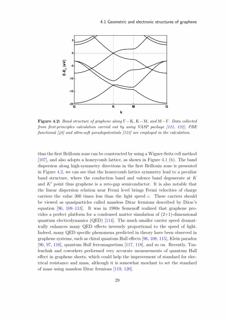
Figure 4.2: Band structure of graphene along Γ−K, K−M, and M−Γ. Data collectedfrom first-principles calculation carried out by using VASP package [121, 122], PBEfunctional [48] and ultra-soft pseudopotentials [123] are employed in the calculation.
thus the first Brillouin zone can be constructed by using a Wigner-Seitz cell method
[107], and also adopts a honeycomb lattice, as shown in Figure 4.1 (b). The band
dispersion along high-symmetry directions in the first Brillouin zone is presented
in Figure 4.2, we can see that the honeycomb lattice symmetry lead to a peculiar
band structure, where the conduction band and valence band degenerate at K
and K ′ point thus graphene is a zero-gap semiconductor. It is also notable that
the linear dispersion relation near Fermi level brings Fermi velocities of charge
carriers the value 300 times less than the light speed c. These carriers should
be viewed as quasiparticles called massless Dirac fermions described by Dirac’s
equation [96, 108–113]. It was in 1980s Semenoff realized that graphene pro-
vides a perfect platform for a condensed matter simulation of (2+1)-dimensional
quantum electrodynamics (QED) [114]. The much smaller carrier speed dramat-
ically enhances many QED effects inversely proportional to the speed of light.
Indeed, many QED specific phenomena predicted in theory have been observed in
graphene systems, such as chiral quantum Hall effects [96, 108, 115], Klein paradox
[96, 97, 116], quantum Hall ferromagnetism [117, 118], and so on. Recently, Tza-
lenchuk and coworkers performed very accurate measurements of quantum Hall
effect in graphene sheets, which could help the improvement of standard for elec-
trical resistance and mass, although it is somewhat mordant to set the standard
of mass using massless Dirac fermions [119, 120].
29

4 Graphene related materials
A question rise naturally when we considered graphene as a two-dimensional crys-
tal? Or how thin does the system is thin enough to become two-dimensional?
Evidently, a graphene monolayer with thickness of one atom is two-dimensional.
Partoens and Peeters have demostrated that the band structure of systems with
eleven or more graphene layers only diverged from that of bulk grahite by 10%,
and the band structure of graphene from monolayer to trilayer evolves from zero-
gap semiconductor to semimetals with evident band overlap [124]. Furthermore,
since the screening length in the normal direction of layers in graphite is about 5
A [125, 126], and the inter-layer distance in graphite is 3.4 A, therefore, graphene
systems with only 5 layers should be discriminated into surface and bulk layers
[96].
Except for the intriguing QED specific nature and usefulness in fundamental
physics, one of the most interesting properties of graphene might be the high charge
carrier concentration even at room temperature and insensitive to the existence
of defects [95, 102, 108, 127]. Accordingly, graphene is a good candidate for the
next generation micro-electronics applications [96, 128]. In fact, many electronic
devices have been predicted or implemented on the basis of graphene, such as filed
effect transistors [129–138], quantum dots [134, 139–141], negative differential re-
sistance (NDR) devices [142, 143], single molecular detector [144, 145], etc. To
take advantages of the nowadays semiconductor technology, the zero-gap graphene
sheets should be tunned to behave as semiconductors and further tuning of the size
of electronic gaps is inevitable. This can be realized by many approaches, includ-
ing spacial confinement [146–150], imposing extra boundary conditions [149–153],
chemical modifications [154–156] and so on.
4.2 Preparation and characterization
Despite graphene has definitely been produced occasionally in the more than 500
years’ history of using graphite as a marking tool or solid lubricant, the first ev-
idence of its existence is the successful exfoliation in 2004, when Geim’s group
repeatedly peel highly oriented pyrolytic graphite (HOPG) mesas, using optical
microscope and atomic force microscope (AFM) to characterize the generated
graphene films [95]. From then on, various approaches have been developed to
prepare graphene, aimed to higher quality, higher throughput and higher yield
[96, 157]. According to whether the preparation procedure involves chemical reac-
tions, we can roughly classify the emerging methods into two kinds, say, chemical
approaches and physical approaches.
30

4.2 Preparation and characterization
4.2.1 Physical approaches
Until now, the highest quality graphene sheets available were prepared by using
the original “micromechanical cleavage” method [95, 102]. Even in their earliest
report, few-layer graphene sheets with dimensions up to 10 µm and thicker flakes
with dimensions up to 100 µm were fabricated successfully. However, the cleavage
method is low yield and low throughput. Another approach is demonstrated by
Coleman’s group, in which graphite powder was first dissolved in organic solvent by
sonication, and then drop the dispersion onto holey carbon. This method results
in a monolayer yield of ∼1 wt%, and potentially be improved to 7-12 wt% [158].
4.2.2 Chemical approaches
The low throughput and yield critically restrict the expansion and development
of graphene investigation and application. Chemists are calling for help to seek-
ing large-scale, cost effective, high yield preparation methods. Be worthy of the
accumulated experiences in carbon chemistry, expecially in the recent decades’ re-
search in graphite, fullerenes and CNTs, various chemical approaches have been
put forward to satisfy the scientific and engineering demands [159].
Chemical exfoliation via redox process
There are also liquid-phase exfoliation methods based on chemical reactions, es-
pecially redox reactions. The first solution based exfoliation approach is demon-
strated by Ruoff’s group in 2006 [160, 161], by molecular-level dispersion of these
chemically modified graphene sheets into solution, followed by mixing with polystyrene
and reduction. The produced graphite oxide is high hydrophilic due to the attached
hydroxyl, epoxide, carbonyl and carboxyl functional groups. In order to prevent
aggregation due to less hydrophilic induced by reduction, electrostatic-stabilization
can be introduced by rasing the pH of the solution [162].
The most conspicuous advantages of solution-phase redox exfoliation methods are
its low cost and high throughput. However, the solubility of graphene sheets often
decreases with the increasing molecular weight, hence limits the produce of large
scale graphene. Moreover, the oxidation and reduction of graphite always destroy
the two-dimensional crystal symmetry of graphene. These two issues should be
addressed in the further investigation [157, 159].
31

4 Graphene related materials
Epitaxial growth and chemical vapor deposition
Graphene can also be prepared by epitaxial growth or chemical vapor deposition
(CVD) methods. One of the earliest transport measurements on few-layer graphene
sheets was performed by de Heer’s group in 2004, where the graphene samples were
grown epitaxially on Si-terminated (0001) surface of 6H-SiC [163, 164]. Depending
on the surface on which graphene grown is terminated by silicon or carbon atoms,
there are two types of graphene prepared by SiC surface epitaxial growth. Usually
graphene monolayer or bilayer is obtained in the former case, moreover, the band
gaps opens as a consequence of graphene-substrate interactions and substrate in-
duced doping and disorder, while the linear dispersion relation retains away Fermi
level [165–167]. In the case of carbon terminated face, multilayer graphene is
preferable to be thermally decomposed on SiC substrate, in which the interlayer
spacing is slightly larger that in bulk crystalline graphite [168, 169]. As a result
of relatively weak electronic coupling between inner layers and strong screening
by surface layers, these samples exhibit electronic properties like free-standing
graphene [166, 169–171].
An alternative route for the epitaxial growth is the use of transition metal substrate
instead of SiC wafer. Epitaxial growth of graphene monolayer or few-layers on Pt
[172], Ir [173], Ni [174–176], and Ru [177, 178] surfaces combined with chemical va-
por deposition (CVD) have been intensively studied in the recent five years. These
CVD approaches rely on the temperature-dependent solubility of interstitial car-
bon atoms in transition metal substrates. Usually hydrocarbons such as methane,
propylene or gas mixtures are decomposed at high temperature and the generated
carbon atoms dispersed in substrate with high solubility, followed by programmed
cooling of the system, carbon atoms would separate out. In this sense, graphene
with wafer sizes might be prepared, indeed, large scale epitaxial graphene with
dimension up to 200 µm has been grown on Ru(0001) surface [178].
bottom-up approach via organic synthesis
The most pronouncing disadvantages of the above mentioned method is the uncon-
trollable character in the preparation process. From the organic chemistry point
of view, graphene possesses a “macromolecue” structure in which sp2 bonding is
distributed homogeneously among carbon frameworks. Hence the development of
a controllable method to prepare graphene sheets could has recourse to an organic
synthesis route.
Mullen’s group demonstrated that graphene nanoribbon-like polyacyclic hydro-
carbons (PAHs) could be synthesized in a bottom-up manner from 1,4-diiodo-
32
4.2 Preparation and characterization
2,3,5,6-tetraphenylbenzene and 4-bromophenylboronic acid [179]. UV/vis adsorp-
tion spectroscopy and mass spectrometry revealed the formation of graphene nanorib-
bon up to 12 nm in length. SEM and STM measurements showed a high self-
assemble tendency of these reactions. However, it is well known that the solubility
decreases and the probability of occurrence of side reactions increases as the molec-
ular weight of reaction product increases, thus extending the size of produced PAHs
remains a big challenge for chemists [157, 179].
4.2.3 Characterization of graphene
One of the most critical reason for the delayed discovery of graphene single or
few-layer sheets is the difficulty in characterizing them. In order to examine the
stack of graphite thin films to find graphene monolayer sheets, an effective approach
works at the micrometer scale should be used. Obviously, the modern visualization
technique depends on scanning probes can not afford this task since their low
throughput. Further more, since the opacity of suspended graphene monolayers is
only 2.3% [105, 180] and is transparent on most substrate, it is difficult to recourse
to optical microscopy. Indeed, AFM has been the only tool to identify graphene
monolayer and few layers, even AFM is only able to distinguish monolayer and
bilayer sheets when the films contain folds or wrinkles [95, 102]. Raman spectra
dawned this issue in 2006 [181], where Raman fingerprints of graphene monolayer,
bilayer and few-layer sheets allow high-throughput, unambiguous identification of
graphene layers. However, Raman spectra still does not allow locating graphene
crystallites in real space. Blake et al. studied the visiblity of graphene monolayer
on SiO2 substrate exposed in visible light with various wavelengths [105]. They
found that graphene on SiO2 can be detected by monochromatic illumination for
any substrate thickness, in addition to 300 nm and ∼100 nm thick SiO2 substrate
are the most effective.
Many other techniques are also used in the characterization of graphene and related
materials, such as X-ray photoelectron spectroscopy (XPS) [182–186], , Fourier
transform infrared resonance (FTIR) [162, 186–190], electron diffraction (ED)
[184], AFM [162, 188, 191], STM [192, 193], TEM [184, 186], nuclear magnetic
resonance (NMR) [183, 184, 186, 188, 194], electron spin resonance (ESR) [186]
and so on. All these techniques play important roles in the characterization of the
structural and electronic properties of graphene.
33

4 Graphene related materials
4.3 Graphene nanoribbons
The high carrier mobility, long phase coherence length of graphene combined with
its two-dimensional planar structure with mechanically stiffness and flexibility open
a new window of potential applications in micro-electronics [96, 128]. However,
the zero-gap character of graphene does not compatible with the mature semi-
conductor technology, where the band gap is necessary with great significance.
Various route seems probable to open band gaps in graphene materials, such as
introducing configurational defects or chemical modification. Among these pro-
posed approaches, spatial confinements realized by cutting two-dimensional sheet
into one-dimensional graphene nanoribbons (GNRs) with specific width, shape,
and edge chirality is the most straightforward way.
4.3.1 Fabrication of GNRs
Owing to the dependence of electronic structure of GNR on its size, shape, chiral-
ity and chemical environment, GNR is expected to be one of the most probable
material to continue Moore’s Law in the next decade [72, 195]. Nevertheless, most
of the applications of graphene in practice relies on the fabrication of GNR in a
controllable manner. So far, a number of approaches have been proposed in the
recent years.
Since the planar structures and the possibility of move or grow graphene onto
traditional wafers, the fully-fledged microlithography technique is expected to be
suit to etching GNRs. Oxygen plasma [196] and electron beam [197] have used
to etch graphene on SiO2 wafers, where hydrogen silsesquioxane (HSQ) was used
as etching mask. However, due to the limit in spacial resolution, lithographic
techniques is unable to fabricate narrow GNRs (less than 10 nm in width) with
smooth edges [196–198]. STM can also be used to tailor graphene sheets into
nanoribbons in a well defined manner. Taking advantage of the atomic resolution
of STM, armchair edged GNRs with width 2.5 nm and energy gap 0.5 eV have
been etched [199]. Yet the low throughput and low yield restrict the application of
STM tailoring technique again. Metallic nanoparticles can also be used as scissors
in the lithographic-etching procedure. Fe [200] and Ni [201] nanoparticles have
been thermally generated and used to cut down graphene into GNRs.
Chemical vapor deposition method can also be used to fabricate GNRs directly.
Campos-Delgado et al. showed that bulk production (grams per day) can be
achieved by pyrolyzing ethanol aerosol containing ferrocene and thiophene in quartz
tubes. GNRs with width 20 ∼ 300 nm and thickness with 2 ∼ 40 layers is obtained
34

4.3 Graphene nanoribbons
[202]. This single-step CVD approach can only fabricate mixtures of few-layer
GNRs with various kinds of edge chirality, further exfoliation is needed to obtain
individual GNR sheets.
There are also solution-phase based approaches in the fabrication of GNRs. Li et al.
demonstrated by dispersing exfoliated graphite in noncovalent polymer solution,
ultrasmooth edged GNRs with width from 50 nm down to sub-10 nm can be
fabricated. Field-effect transistor-like devices can be constructed based on these
solution-phase derived GNRs, and an on-off ratio of about 107 is obtained at room
temperature [203].
Carbon nanotubes can be stated as rolled-up graphene sheets with corresponding
C-C bonds rejoined, inversely, CNTs can also be unzipped forming GNRs. Jiao et
al demonstrate that multi-walled carbon nanotubes (MWCNTs) can be unzipped
into GNRs with smooth edges, controllable width and more importantly, high
yield. MWCNTs were embedded in poly(methyl methacrylate) (PMMA) layer
mask, and leaving a side exposed to Ar plasma. Hence the exposed side would
be etched faster than the others and result in unzipped CNTs [204]. The most
pronouncing advantage of the CNT unzipping approach are its controllable width
and edge chirality, in addition to high yield. However, using CNT as raw material
lead to low cost-effectiveness compared with other fabrication methods.
4.3.2 Structural and electronic properties of GNRs
Depending on the crystallographic direction of edges (edge chirality), there are two
kinds of typical GNRs as shown in Fig. 4.3: GNRs with armchair edges (AGNR)
and zigzag edges (ZGNR). The width W of GNRs can be defined as the number
of C–C dimers or zigzag chains in the transverse direction of AGNR or ZGNR,
respectively. Thus the GNRs in Fig. 4.3 can be noted as 15-AGNR (a) and 8-
ZGNR (b), respectively, where the numbers 15 and 8 denote the width of system.
Since the carbons in pristine graphene are sp2 hybridized, there is one dangling
bond for each carbon atom at the edges of GNRs. Hydrogen atoms are usually
used to saturate these dangling bonds of edge carbon atoms in real calculations
[146–150, 152–155, 205].
It was 1996, ten years before the successful fabrication of GNRs, Fujita et al.
investigated the electronic structures of ZGNRs and AGNRs based on nearest
neighboring tight-binding (TB) method [206, 207]. First principles calculation of
the band structures of ZGNRs that confirmed the TB results of ZGNRs at density
functional theory (DFT) level using localized density approximation (LDA) [205].
In the nearest neighboring TB simulations, only two parameters, the on-site energy
35

4 Graphene related materials
Figure 4.3: Schematic of structures of GNRs. (a) Armchair edged GNR with widthW=15, 15-AGNR; (b) Zigzag edged GNR with width W=8, (8-ZGNR).
and the hoping integrals, are considered, where the later corresponding to the sp2
interactions between two neighboring carbon atoms. All the ZGNRs are predicted
as metallic due to the two edge states from each edge degenerate when k ≥ 2π/3a
in the first Brillouin zone. On the other hand, the energy gaps of AGNRs change
with the width and behaves a family behavior with width period of 3: systems
with width W = 3p + 2 are metallic and others are semiconductor, where p is an
integer [206].
Son et al. thoroughly examined the electronic structures of GNRs with hydrogen
saturated edges by performing first principles calculations. They found that all the
AGNRs are semiconductors with energy gaps inversely scales with system width
[146, 147], nevertheless, the family behavior of the tendency of energy gaps change
with system width reserves, except AGNRs with width W = 3p + 2 and 3p + 1
possess the smallest and largest energy gaps among a period, respectively. Fur-
ther GW quasiparticle calculations demonstrated that the energy gaps are about
three times larger than those from LDA calculation [148], by the virtue of treating
electron correlation more carefully [31, 33].
More interestingly is the case of ZGNRs, the metallic state was reproduced by
a spin-unpolarized calculation with two edge states degenerated at Fermi level.
However, this paramagnetic state is not the ground state with 20 meV per edge
36

4.3 Graphene nanoribbons
carbon atom higher than that of the antiferromagnetic state for 8-ZGNR. More-
over, the spin degeneration would be removed by introducing a transverse electric
field perpendicular with the periodic direction in system plane, where one of the
valence band and conductance band of one spin orientation would overlap and left
the other semiconducting, leading to a half-metallic character [149, 149]. The ex-
ternal transverse electric field can be generalized to an internal one introduced by
chemical functionalization of carbon atoms at each edge with electron withdrawing
and donating groups. ZGNRs with one side decorated by NO2 and the other by
CH3 groups were predicted to be half-metallic [155].
Chemical modification [156, 208] and strain effects [153] to the electronic properties
of GNRs have also been examined theoretically.
37


5
Inelastic Electron Tunneling in
Surface-Adsorbate Systems
As a sub-discipline of physics or an inter-discipline of physics, chemistry, material
science and biology, surface and interface science attracted tremendous interests
in the recent decades, and plays more and more important roles both in the fun-
damental and applied research. In fact, surface science is already a fundamen-
tal discipline in the research activities in, for example, semiconductor technology,
catalysis, epitaxial growth, life science, and so on [84, 209]. Indeed, the thoroughly
understanding of growth mechanisms at a microscopic scale is essential for the de-
sign and application of novel materials; Adsorption and desorption, the elementary
processes in surface science, are the basis of heterocatalysis; A substrate is also
inevitable in the integrating of molecular devices into circuits. All this kind of
demands in frontier researches boomed the rapid growth of surface and interface
science [209].
5.1 Surface science and STM
Researchers have made colossal progresses in the studies of surface and interface
systems, especially at a microscopic level: In the experiment aspect, there are a
number of powerful microscopy technologies have been invented and applied in
daily research. Scanning tunneling microscope (STM) is the most notable exam-
ple, by which single atom or single molecule and its trace on the surface can be
characterized in a real-time manner, moreover, chemical bonding can also be ma-
nipulated by using STM [90]; In the simulation aspect, the progress in calculation
ability and the spring up of solid and efficient computational methods provides
39

5 Inelastic Electron Tunneling in Surface-Adsorbate Systems
Figure 5.1: Simulated STM constant current image of HOPG. The carbon lattice of thetopmost layer is placed underneath the image to mark the positions in real space. LDOSdata collected from first-principles calculation carried by VASP package [121, 122], PBEfunctional [48] and ultra-soft pseudopotential are used in the calculation. The LDOS isintegrated from density of states in the energy range [0,0.25] eV respect to Fermi energy.
the possibility of full-quantum mechanical description or dynamics simulation of
interested systems.
The exact characterization system is a prerequisite for any investigations, however,
it is not a trivial work in surface and interface science, as a result of the large surface
atom ratio, the existence of dangling bond, surface sates, geometric reconstruction,
and chemical modification, etc. The invention of STM overcame many of these
difficulties. In 1983, Binnig and coworkers scanned the first STM image of the
reconstructed Si(111)-7×7 surface in real space [10], and thus resolved the Si(111)
surface reconstruction puzzle perplexed people for more than twenty years since its
discovery [210]. However, as mentioned in Chapter 3.2.1, the STM images reflect
spatial distribution of density of electronic states, but not the surface topography.
As a result, there is no direct correspondence between STM images and positions
of atoms on surface. One of the most famous examples might be the STM constant
current images of highly oriented pyrolytic graphite (HOPG) surface as shown in
Figure 5.1, in which only three protrusions are observable in an area corresponding
to a hexagonal ring [211].
By means of the ultimate high resolution and the ability to provide structural
information in real space, STM made enormous contributions to the investigation
of surface systems. The atomic resolution in real space brought the possibility of
performing single atomic or single molecular experiments, which is very significant
in the following aspects: First, atoms and molecules are elementary particles in
chemistry, which preserve the chemical properties of substance; Next, there is no
ensemble average in single molecular experiments, which is significant in macro-
40

5.2 STM mediated inelastic tunneling spectra
scopic experiments; Third, the effects of environment that system experienced are
relatively largely enough to be detected in experiments; Fourth, the observation of
quantum objects such as atoms or molecules implies that it is possible to manipu-
late them or their interactions – chemical bonding [90]. On the other hand, these
features bring trouble to the understanding of single molecular phenomena: As
the consequence of the absence of ensemble average, fluctuations between different
measurements are evident and numerous repeatedly measurements are necessary
for a reliable result, this is just the cases for STS experiments in which most of the
reported results are averaged among a number of repeated experiments; The sys-
tem is so small that some of its properties are sensitive to perturbations from the
environment, sometimes even qualitatively. One example is the system melamine
tautomers adsorbed on Cu(100) surface, in which the orientation of top N-H bond
varies when electron pulse is imposed, however, this change in orientation of a
single chemical bond lead to distinct current-voltage characteristics [73]. In this
aspect, theoretical simulation is able to eliminate the ambiguities introduced by
random perturbation, and plays an important role to reveal the underlying physics
and chemistry of surface phenomena.
5.2 STM mediated inelastic tunneling spectra
STM mediated inelastic tunneling spectra (STM-IETS) becomes more and more
important in the recent several years. IETS reflects the vibration features of sys-
tem, which is sensitive to the chemical composition, structural configuration, and
conformation of system. The first IETS experiment was performed by Jaklevic
and Lambe in 1966 [212], where the authors buried molecules into the interface
of a metal-oxide-metal tunneling junction, and measured its I-V characteristics.
A suddenly change in conductance occurs when the injection energy of electrons
(say, the bias voltage) is large enough to overcome the excitation energy of a spe-
cific vibration mode of the molecules. This change in conductance arises from
inelastic electron tunneling process, in which extra tunneling channels opened by
electron-phonon scattering. However, the first single molecular IETS experiment
was conducted only eleven years ago, by W. Ho’s group, where a STM is employed
to excite the vibration modes of acetylene molecules and measure the conductance
change [213, 214].
Since the vibration features are fingerprint properties of molecules, functional
groups, clusters, and even more complex systems, such as surface-adsorbate sys-
tems, in this aspect, at a single molecular level, STM-IETS relies heavily on the
reconstruction of substrate surface, the chemical composition of adsorbates, the
41

5 Inelastic Electron Tunneling in Surface-Adsorbate Systems
adsorption site, configuration, conformation and orientation, the molecule — sur-
face interactions, and inter- or intra-molecular interactions (if any), etc [215]. In
addition, the tunneling current would definitely effect the system in an STM ex-
periment, exciting electrons [62, 64, 65] or phonons [24, 216, 217] or leading to
adsorption/desorption processes [218, 219], combined with the disability to obtain-
ing surface topography. Usually it is difficult to characterize the system merely by
STM images and STS. STM-IETS then undertakes the mission to eliminate these
ambiguities and performs chemical characterization at single molecular level.
For a concrete impression for the efficiency and power of STM-IETS in chem-
ical characterization at atomic level, I would like to cite the experimental and
theoretical works about the identification of the products by benzene molecules
dehydrogenation on Cu(100) surface [220, 221]. The STM induced benzene de-
hydrogenation experiment was performed by L. J. Lauhon and W. Ho in 2000,
where the STM topographic images and IETS of benzene molecule and its dehy-
drogenated products on Cu(100) surface were measured, and then those results
were compared with that of pyridine (C5H5N) on the same surface. Based on
the similarity between the symmetry of STM images and C-H(D) peak locations
in STM-IETS, the authors non-conclusively proposed that the reaction products
might be benzyne fragment (C6H4) with two hydrogen atoms dissociated [220].
However, thoroughly theoretical simulations of the topographic images and STM-
IETS by Bocquet, Lesnard and Lorente demonstrated that the topographic images
of a benzene molecule lying on Cu(100) surface, and a phenyl (C6H5) or benzyne
fragments stand upon the bridge site of Cu(100) surface are hardly distinguish-
able due to their similar symmetry. However, the IETS features corresponds to
C-H stretching modes of each of these adsorbates is distinctive. By comparing
with the simulated STM-IETS with the measured ones, the authors conclude that
the benzene dehydrogenation product is a phenyl fragment rather than a benzyne
fragment [221].
5.3 Simulation of STM-IETS
Many approaches aimed to describe the tunneling process in STM measurement
emerged since the invention of this revolutionary instrument [88, 222]. Depending
on how to treat the tip-sample interactions, these approaches can be classified as
semi-classical or quantum mechanical. For the semi-classical approaches, the vac-
uum gap between tip and sample is considered as a slowly varying potential through
which electrons tunneling between tip and sample. This method is firstly proposed
by J. Bardeen and was named Bardeen approximation, where the tip electronic
42
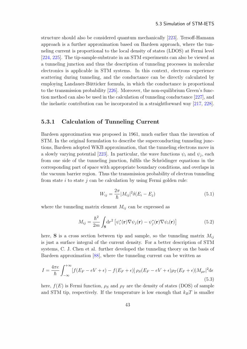
5.3 Simulation of STM-IETS
structure should also be considered quantum mechanically [223]. Tersoff-Hamann
approach is a further approximation based on Bardeen approach, where the tun-
neling current is proportional to the local density of states (LDOS) at Fermi level
[224, 225]. The tip-sample-substrate in an STM experiments can also be viewed as
a tunneling junction and thus the description of tunneling processes in molecular
electronics is applicable in STM systems. In this context, electrons experience
scattering during tunneling, and the conductance can be directly calculated by
employing Landauer-Butticker formula, in which the conductance is proportional
to the transmission probability [226]. Moreover, the non-equilibrium Green’s func-
tion method can also be used in the calculation of tunneling conductance [227], and
the inelastic contribution can be incorporated in a straightforward way [217, 228].
5.3.1 Calculation of Tunneling Current
Bardeen approximation was proposed in 1961, much earlier than the invention of
STM. In the original formulation to describe the superconducting tunneling junc-
tions, Bardeen adopted WKB approximation, that the tunneling electrons move in
a slowly varying potential [223]. In particular, the wave functions ψi and ψj, each
from one side of the tunneling junction, fulfils the Schrodinger equations in the
corresponding part of space with appropriate boundary conditions, and overlaps in
the vacuum barrier region. Thus the transmission probability of electron tunneling
from state i to state j can be calculation by using Fermi golden rule:
Wij =2π
h|Mij|2δ(Ei − Ej) (5.1)
where the tunneling matrix element Mij can be expressed as
Mij =h2
2m
∫
S
dr2[ψ∗
i (r)∇ψj(r)− ψ∗j (r)∇ψi(r)
](5.2)
here, S is a cross section between tip and sample, so the tunneling matrix Mij
is just a surface integral of the current density. For a better description of STM
systems, C. J. Chen et al. further developed the tunneling theory on the basis of
Bardeen approximation [88], where the tunneling current can be written as
I =4πe
h
∫ +∞
−∞[f(EF − eV + ϵ)− f(EF + ϵ)] ρS(EF − eV + ϵ)ρT (EF + ϵ)|Mµν |2dϵ
(5.3)
here, f(E) is Fermi function, ρS and ρT are the density of states (DOS) of sample
and STM tip, respectively. If the temperature is low enough that kBT is smaller
43

5 Inelastic Electron Tunneling in Surface-Adsorbate Systems
than the energy resolution in measurement, the tunneling current can be approxi-
mated as
I =4πe
h
∫ eV
0
ρS(EF − eV + ϵ)ρT (EF + ϵ)d|Mµν |2ϵ (5.4)
by approximating the value of Fermi functions for occupied and unoccupied states
are 1 and 0, respectively. We can further approximate that the tunneling matrix
elements Mij varies only slightly in the experimental energy range, then we have
I ∝ 4πe
h
∫ eV
0
ρS(EF − eV + ϵ)ρT (EF + ϵ)dϵ (5.5)
that is to say, the tunneling current is just the convolution of the DOS of two
subsystems, which implies the measured physical quantity in STM experiment is
DOS.
The effects of STM tip to the measurements were usually found to be neglectable
in many experiments, which is also expected by people that the deviation from
different tips can be omitted. Tersoff and Hamann proposed a simple STM tip
model of which the wave functions are spherical symmetric s-type states [224, 225],
they use Sommerfeld model for metals to simulate the spherical tip, as shown in
Figure 5.2. The tunneling matrix element Mij at low bias can then be calculated
by subject the analytical expression of s-type orbitals
Mij =2πh2
mκΩ−1/2tip κR exp(κR)ψj(r0) (5.6)
where Ωtip is the normalized volume of STM tip, r0 is the radius of curvature of
tip, κ =√
2m(U − E)/h is the inverse decay length of wave functions. Thus the
tunneling current at bias V is
I ∝∫ EF +eV
EF
ρS(r, E)dϵ (5.7)
Differentiating tunneling current respect to bias voltage, the tunneling conductance
is obtaineddI
dV∝ ρS(r, EF ) (5.8)
Eq. 5.8 is Tersoff-Hamann approximation. From Eq. (5.7) and Eq. (5.8), we can
see that the constant current STM images reflect the contour LDOS of sample at
Fermi level. With the help of Tersoff-Hamann approximation, it is easy to explain
STM measurements qualitatively, and has been used in various systems, such as
semiconductor surfaces, surface-adsorbate systems, tunneling heterojunctions, and
so on [229].
44

5.3 Simulation of STM-IETS
Figure 5.2: Schematic of tunneling junction in STM experiments. The STM tip mightadopt various shapes, except for the lowest part is a hemisphere with radius of curvatureR.
5.3.2 Inelastic electron tunneling
Boosted by the rapid growth in STM-IETS experiments, there have been several
theoretical works concentrate on the simulation of inelastic tunneling process in
STM systems. Lorente and coworkers developed a scheme to calculate the elastic
and inelastic contributions to tunneling conductance based on Tersoff-Hamann ap-
proximation and Bardeen approximation [24, 230, 231], and revealed the symmetry
selection rules in STM-IETS [232]. A unified description of propensity rules for
IETS has also been proposed by Paulsson et al. [228]. Mingo and Makoshi devel-
oped a Green’s function based method to calculate the inelastic electron tunneling
[217], NEGF methods appropriate for molecular junctions can also be used in STM
systems[233–236]. In addition, many works combined theoretical simulation and
experimental measurement also emerged [221, 237–242].
In the following, I shall describe the scheme to calculate STM-IETS we imple-
mented based on Tersoff-Hamann approximation using finite difference method.
Most of the formula were derivated along the original work by Lorente et al.
[24, 25, 230, 231].
In Tersoff-Hamann approximation [224, 225], the tunneling conductance is propor-
tional to the LDOS of sample at Fermi level,
dI
dV(r) ∝ ρ(r, EF ) =
∑
n,k
|⟨r|Ψn,k⟩|2 δ(εn,k − EF ) (5.9)
45

5 Inelastic Electron Tunneling in Surface-Adsorbate Systems
here, ρ(r, EF ) is the LDOS at Fermi energy at position r, Ψn,k is the n-th wave
function with k-vector k whose eigenenergy is εn,k. The Delta function is substi-
tuted by a Gaussian in practical calculations, the broadening parameter could be
selected by considering practical experimental parameters, such as temperature,
energy resolution, etc.
Since STM-IETS originated from the vibrational excitation induced by inelas-
tic tunneling electrons, in the framework of Tersoff-Hamann approximation, the
change in tunneling conductance would be proportional to the change in the LDOS
induced by the corresponding vibration mode,
d2I
dV 2
∣∣∣∣Qi
∝ |δρ(r, EF )|2
=∑
n,k
[2ℜ⟨Ψn,k|r⟩⟨r|δΨn,k(Qi)⟩+ |⟨r|δΨn,k(Qi)⟩|2
]δ(εn,k−EF
)
= δρI + δρII
(5.10)
where δρ(r, EF ) is the change in LDOS at Fermi level at position r, |δΨn,k(Qi)⟩ is
the change in wave function |Ψn,k(Qi)⟩ induced by the ith vibration mode Qi.
From Eq. (5.10), we note that the intensity of IETS is contributed by two terms,
i.e. the first and second terms generated by finite difference, and are odd and even
parities, respectively. Taking into account of the arbitrariness in the assigning of
positive direction of vibration modes, combined with the same weight of positive
and negative directions, the contributions from the first order term vanishes, and
only δρII is needed in our calculation.
By using finite difference method, the changes in wave functions are linearly de-
pendent on the small displacement of ions’ positions, thus we can write out the
wave functions of systems experienced small configurational distortions [231],
|Ψ+n,k(fQi)⟩ = |Ψ0
n,k⟩+ fQi|Ψ0n,k⟩
= |Ψ0n,k⟩+ f |δΨn,k(Qi)⟩
|Ψ−n,k(fQi)⟩ = |Ψ0
n,k⟩ − fQi|Ψ0n,k⟩
= |Ψ0n,k⟩ − f |δΨn,k(Qi)⟩
(5.11)
where |Ψ0⟩ is the wave functions of the equilibrium configuration, and |δΨ(Qi)⟩is its change along Qi. The parameter f is introduced to ensure the validity of
harmonic approximation. Benchmark calculations using f = 0.1, 0.2, 0.5, and 1.0
demonstrated that there is no qualitative difference between these tests [243].
46

5.3 Simulation of STM-IETS
The change in wave functions can then be obtained by combining the equations in
Eq. (5.11):
|δΨn,k⟩ =1
2f
[|Ψ+
n,k(fQi)⟩ −|Ψ−
n,k(fQi)⟩⟨Ψ+
n,k(fQi)|Ψ−n,k(fQi)⟩
](5.12)
here, |Ψ−n,k⟩ is projected on the direction of |Ψ+
n,k⟩ to eliminate the phase difference
between wave functions in different systems.
47

6
Summary of papers
In this chapter, I would like to give a brief summary of the listed papers in this
thesis. All the works are classified into two part, the first is molecular electron-
ics, including device design and theoretical simulation of DNA sequencing using
conductance difference; The second part is inelastic electron tunneling spectra in
surface-adsorbate systems. I shall introduce our benchmark results first, and fol-
lowed by the performance of our STM-IETS code in two typical surface-adsorbate
systems, carbon oxide adsorbed on Cu(100) surface and acetylene adsorbed on
Cu(1000), which have been widely studied both by experiments and theoretical
simulation. Then two applications combined with the latest STM-IETS experi-
ments will be presented.
6.1 Molecular electronics
There are two works in this section, one is the theoretically design of negative
differential resistance (NDR) device based on armchair edged graphene nanorib-
bons (AGNR); the other is a theoretical study of the electron transport of DNA
base pairs based molecular junctions, in the latter study, we concentrate on the
structural effects on transport properties.
6.1.1 AGNR as a NDR device
All the AGNRs are semiconductors with energy gaps inversely proportional to its
width [146, 148, 244]. Combined with the high carrier mobility and long phase
coherence length [96, 157], it is expected that ballistic transport would occur in a
considerable large device constructed by graphene.
49

6 Summary of papers
In paper I, we designed a NDR device based on selectively doped AGNRs. The
doped nitrogen atoms introduce doping states in the energy gap of the electrodes,
and lead to sharp DOS peaks in the corresponding energy range. On the other
hand, in the scattering region, discrete energy levels appear due to the finite size.
In the resonant tunneling regime, the DOS peaks in the left and right electrodes
shit up and down with a value eV/2 when a bias voltage V is applied across the de-
vice. In consequence, the tunneling channel would be constructed or destructed at
different bias, and there would be a bias range that the channels are constructed at
lower bias and are destructed when the bias increases, which will lead to a decrease
in tunneling current, and exhibits as negative differential resistance phenomenon.
We have investigated devices consists of AGNRs with various widths and of various
lengths of scattering region, the results shows the larger of the energy gap of
undoped electrode, and the shorter the scattering region, the more evident the
NDR peak. This can be easily understood that from one side, the doping DOS
peak would be sharper when the gap of undoped system is larger; from the other
side, the energy intervals between discrete electronic states in the scattering region
would be larger when the size is smaller. Both of these issues contribute to a more
dramatic change in tunneling channel construction, and lead to a more evident
NDR peak.
6.1.2 Structural factors controlling the conductance of DNA
pairs junctions
The widely use of DNA technique in life science and medicine industrial demands
a cost-effective DNA sequencing method, the well established electric/electronic
techniques seems and is expected to be an effective approach in this aspect. Re-
cently, Lindsay’s groups proposed a method to sequencing DNA base pairs by using
STM to measure the conductance decay respect to tip-substrate distance [22, 23].
Molecular junctions composed by STM tip, DNA base pair (AT or GC), and
substrate are constructed in the experiments. At the mean time, the tunneling
currents were recorded as stretching the STM tip. Since the number of hydrogen
bonds (H-bonds) between base pairs in AT and GC are two and three, respectively,
thus AT pairs might be more flexible than GC pairs. In the experiment, the authors
self-assembled one of the base group on gold surface and held the other with STM
tip, the current decay curves evolves from the largest current to about zero last
more than and less than 2 nanometers, for 3-H-bonds and 2-H-bonds junctions,
respectively. Thus the number of H-bonds can be identified by comparing the
50

6.2 Inelastic tunneling spectra
current-distance decay curves between different base pairs, and DNA sequencing
is achieved by electric measurement [22, 23].
However, it is well known that the effective distance of H-bonds is about 0.25 nm,
which is much smaller than the decay lengths in the experiments (about 2 nm),
hence we believe that the difference between decay curves in the experiment is
not a consequence of the different number of H-bonds, other causes of this phe-
nomenon should be addressed. In paper II, by performing first-principles geometry
relaxation and transport calculation, we conclude that the experimentally observed
distance dependent tunneling current difference between DNA base pair junctions
are not caused by different number of H-bonds but by the different stacking struc-
tures. Furthermore, we found that this electrical read-out technique is probably
useful although the experimental measurements are not exact enough.
6.2 Inelastic tunneling spectra
I shall briefly describe three of my works in this section, at first I’d like to introduce
the method implementation and benchmarks, and then two applications of our code
followed, both of them are combined with the latest experimental works.
6.2.1 Method implementation and benchmarks
We implemented the simulation method described in Section 5.3 on the basis of
converged electronic structures of VASP package [121, 122], in which the wave
functions is expanded in a plane wave basis set with a sufficient large energy
cutoff, projector augmented wave (PAW) [245] is used to describe the electron-ion
interactions in the calculations. The dynamic matrix is constructed by “selective
dynamics” supplied by VASP by confining positions of ions in lower layers.
In the plane wave representation, the wave functions is linear combinations of a
set of plane waves,
|Ψn,k⟩ =
Nk∑
i
ci,n,k|k + Gi⟩ (6.1)
where ci,n,k is the linear combination coefficients, Gi is the i-th wave vector of a
plane wave, it is an integer multiple of reciprocal lattice vectors
Gi = nxib1 + nyib2 + nzib3 (6.2)
51

6 Summary of papers
here, nσi is the i-th integer multiples in direction σ, and the reciprocal lattice
vectors can be calculated from lattice vectors in real space
aibj = 2πδij (6.3)
Nk in Eq. (6.1) is the number of plane waves at a specific k of the k-sampling in
the first Brillouin zone, and depends on the energy cutoff Ec
h2|k + GNk|2
2me
≤ Ec (6.4)
Since the plane waves are mutually orthonormal, only the coefficients need to be
operated in the calculation of STM-IETS in our code.
We have tested our code in two typical surface-adsorbate systems, which have
been widely investigated by experimental and theoretical means. Indeed, these
two system are also the earliest studied in the single molecular IETS area [213,
214, 246, 247].
CO molecule adsorbed on Cu(100) surface
The single molecular STM-IETS measurement of CO was first carried out by L.
Lauhon and W. Ho in 1999 [246], in which CO and its isotopic substitute adsorbed
on Cu(100) and Cu(110) surfaces. There are three peaks in the STM-IETS of
various isotopic substituted CO molecules adsorbed on both surfaces, which are
located at ∼20 meV, 36.3(33.2) meV, and 256 meV, and corresponding to Cu
surface vibration, two degenerated hindered rotation modes, and C-O stretching
mode, respectively. The CO-Cu stretching mode is not detectable in STM-IETS
experiments, which can be explained by the symmetry selection rules proposed
by Lorente et al. [232]. The spatial distribution of IET signals from hindered
rotation modes has also been scanned, and appeared as a protrusion centered at
the molecular axis [246].
In our benchmark calculations, we reproduced the STM-IETS and spatial distribu-
tions of IET signals induced by the hindered rotations and C-O stretching mode,
our results agreed very well with the experimental ones and previous theoretical
simulations [231].
Acetylene molecule adsorbed on Cu(100) surface
Acetylene (C2H2) and its deuterates (C2D2 and C2HD) adsorbed on Cu(100) and
Ni(100) surface are also widely studied both by experimental and theoretical tech-
52

6.2 Inelastic tunneling spectra
niques [24, 213, 214, 217, 232, 247]. We used a series of acetylene molecules ad-
sorbed on Cu(100) surface as another typical system to benchmark our code.
It is found experimentally only peaks corresponding to C-H or C-D stretching
modes are detectable in the STM-IETS measurement. There is one peak in
C2H2@Cu(100) and C2D2@Cu(100), and two peaks in C2HD@Cu(100), where the
degeneracy between symmetric and antisymmetric C-H or C-D stretching modes
is eliminated by isotope effect [214]. In the meantime, IET signals only appear
when the injecting electrons possess energy just enough to excite a observable vi-
bration mode of the system [214]. Reversible rotation of the adsorption orientation
can also be achieved by inelastic electron excitation, where energy transfer from
C-H (C-D) stretching mode to the hindered rotation mode [213]. The IET sig-
nals were found to be spatially localized to the bonds which are responsible to the
corresponding vibration modes, this phenomenon can be verified by scanning the
spatial distribution of C-D stretching signals in C2HD@Cu(100) [247]. Further-
more, the C-H (C-D) stretching peak for C2H2 (C2D2) is mainly contributed by
the antisymmetric stretching mode, which is a consequence of the selection rules
[232].
Our benchmark simulations reproduced all the STM-IETS spectra and IET spa-
tial maps, all of our results are in good agreement with the previous theoretical
works[24, 217, 232].
6.2.2 Identifying adsorption configuration and orientation
of cis-2-butene adsorbed on Pd(110) surface
There are four equivalent adsorption orientations for the system cis-2-butene molecule
adsorbed on Pd(110) surface, as a result of both the symmetry of adsorbate and
substrate as shown in Figure 6.1. Sainoo and coworkers obtained the STM im-
ages of this system with each orientation, and found that these STM images can
be mutually transformed to each other under STM induced inelastic excitation,
which implies that the adsorption orientation can be reversibly varied [248].
The STM image of cis-2-butene molecule adsorbed on Pd(110) surface consists of
two parts: a head with a larger bright spot and a tail with a smaller and less bright
spot [248, 249]. By assuming the head corresponds to the two higher CH3 groups
and the tail corresponds to the relatively lower C=C double bond bonding to a Pd
atom at on-top site, the dynamics of orientation transformation induced by STM
inelastic excitation was revealed. Two vibration features are observable in STM-
IETS, i.e. C-H (C-D) stretching modes at 358 (268) meV and molecule-surface
stretching modes at 36 (32) meV for C4H8 (C4D8), both features are responsible
53

6 Summary of papers
Figure 6.1: Schematic view of the structure of one of the four equivalent adsorptionorientations of cis-2-butene molecule adsorbed on Pd(110) surface.
to the suddenly increase in the yield in orientation transformation recorded as
increasing bias voltage [248].
However, our calculation gives a different topographic image versus adsorption
orientation relations. In our simulation, the head of topographic image corresponds
to the CH3 group protrude along the Pd line of Pd(110) surface [(110) direction],
and the tail corresponds to the other CH3 group protrude normal to the Pd line
[(001) direction]. To verify our results, we carried out STM-IETS simulations and
compared with the experimental ones. STM-IETS were measured at the center of
the head in topographic images. According to claimed by experimenters, IETS was
measured at the midpoint of the line joining up the highest hydrogen atoms belong
to each CH3 groups. According to our simulation, IETS was measured above the
hydrogen atom of the CH3 group in (110) direction. By comparing the calculated
IETS at these two positions with the measured ones, the actual image-orientation
correspondence can be verified.
6.2.3 Melamine tautomers adsorbed on Cu(100) surface
Controlling the electron transport properties at single molecular level is inevitable
for the practical application of molecular electronics. Pan and Fu et al. demon-
54

6.2 Inelastic tunneling spectra
strated that the transport properties of melamine tautomers adsorbed on Cu(100)
surface can be controlled by imposing current pulse by using STM [73]. When
melamine molecule is adsorbed on Cu(100) surface, two of its attached hydrogen
atoms at the same side of the triangular would be dissociated, and the molecule
would stand upon the bridge site of Cu surface with two N-Cu bonds for each nitro-
gen atoms at the dehydrogenated side. The adsorption configuration is presented
in Figure 6.2 D and E, and its topographic image exhibit a symmetric “dumbbell”
shape as shown in Figure 6.2 A and B (molecule 2). One of the top hydrogen
atoms can be transferred to the shoulder site of the adsorbed molecule by impos-
ing further pulse, and the orientation of the left top N-H bond is free to change
under electron pulse. These two melamine tautomers, named as melamine-C1 and
melamine-C2, whose adsorption configurations are presented in Figure 6.2 F and H,
respectively. The topographic images of C1 and C2 exhibit as asymmetric “cashew
nut” with different opening direction [73]. Furthermore, the I-V curves for C1 and
C2 evidently differ to each other, where for the one hand, C2 possesses a rectifier
character in which electrons tunneling from sample to STM tip is preferable, in
addition, the tautomers behave like a switch with on and off states corresponding
to C1 (C2) and C2 (C1) for positive (negative) bias, respectively [73].
Despite the manifold distinctions between melamine-C1 and C2, especially in the
I-V characteristics, it is difficult to identify these two states merely by STM topo-
graphic images, in which the shapes are exactly the same, and only the opening
directions are different. STM-IETS measurements were carried out towards single
molecular chemical identification. As a result of the difference in relative orien-
tations of N-H bonds on the top and shoulder site of melamine tautomers, the
out-of-plane swinging mode redshifted from 105 meV in melamine-C1 to 97 meV
in melamine-C2. This difference can be directly reflected by STM-IETS, by per-
forming IETS simulations, the proposed mechanism for melamine tautomerization
induced single molecular rectifying and switching in Ref. [73] is verified.
55

6 Summary of papers
Figure 6.2: Rectifying and switching behavior of a modified single melamine molecule.(A and B) STM topographic images of the same area (V = 0.2 V, I = 0.5 nA) inwhich molecules 1 and 3 are activate by applying a +2.4 V pulse on each of them. Theblack dots marked on the images give the STM tip position at where all conductancemeasurements are taken. Inset, STM images acquired with a sample bias of -0.8 V. Thescale for apparent high of the molecule is given. (C) I-V curves measured for Cu (black),melamine (red), and melamine-C (blue). Fluctuation features are shown in the inserts.(D and E) top and side views, respectively, of the computational model for the melamineadsorbed on Cu(100). The dashed line represents the unit cell. Calculated STM imagesof the optimized structures of melamine-C1 (F) and melamine-C2 (H) are given in Gand I, respectively (at V = - 0.6 V and height of 7 A from metal substrate). (J) Thecalculated I-V curves for dehydrogenated melamine, melamine-C1, and melamine-C2 onCu(100). Reprinted with permission from Ref. [73]. Copyright (2009) National Academyof Sciences, U.S.A.
56

References
[1] E. Schrodinger, Br. J. Philos. Sci., III, 233, 1952.
[2] R. P. Feynman, Caltech’s Engineering and Science, 23, 22, 1960.
[3] P. A. M. Dirac. The principles of quantum mechanics. Oxford University Press,Oxford, 4th edition, 1958.
[4] P. A. M. Dirac, Proc. Roy. Soc. A, 123, 714, 1929.
[5] D. R. Hartree, Proc. Cambridge Phil. Soc., 24, 426, 1928.
[6] P. Hohenberg and W. Kohn, Phys. Rev., 136, B864, 1964.
[7] W. M. C. Foulkes, L. Mitas, R. J. Needs, and G. Rajagopal, Rev. Mod. Phys.,73, 33, 2001.
[8] P. W. Anderson, science, 177, 393, 1972.
[9] A. Aviram and M. A. Ratner, Chem. Phys. Lett., 29(2), 277, 1974.
[10] G. Binnig, H. Rohrer, C. Gerber, and E. Weibel, Phys. Rev. Lett., 50(2), 120,1983.
[11] G. Binnig, C. F. Quate, and C. Gerber, Phys. Rev. Lett., 56(9), 930, 1986.
[12] C. J. Muller, J. M. van Ruitenbeek, and L. J. de Jongh, Physica C: Superconduc-tivity, 191(3-4), 485, 1992.
[13] H. Park, A. K. L. Lim, A. P. Alivisatos, J. Park, and P. L. McEuen, Appl. Phys.Lett., 75(2), 301, 1999.
[14] M. A. Reed, C. Zhou, C. J. Muller, T. P. Burgin, and J. M. Tour, Science,278(5336), 252, 1997.
[15] M. Di Ventra, S. T. Pantelides, and N. D. Lang, Phys. Rev. Lett., 84(5), 979,2000.
57

REFERENCES
[16] Y. Xue. Molecular electronic devices: Electronic structure and transport properties.PhD thesis, Purdue University, 2000.
[17] J. Taylor, H. Guo, and J. Wang, Phys. Rev. B, 63(24), 245407, 2001.
[18] M. Brandbyge, J. Mozos, P. Ordejon, J. Taylor, and K. Stokbro, Phys. Rev. B,65(16), 165401, 2002.
[19] S. H. Ke, H. U. Baranger, and W. Yang, Phys. Rev. B, 70(8), 085410, 2004.
[20] A. R. Rocha, V. M. Garcıa-Suarez, S. Bailey, C. Lambert, J. Ferrer, and S. Sanvito,Phys. Rev. B, 73, 085414, 2006.
[21] J. Jiang, M. Kula, and Y. Luo, J. Chem. Phys., 124(3), 034708–10, 2006.
[22] J. He, L. Lin, P. Zhang, and S. Lindsay, Nano Lett., 7(12), 3854, 2007.
[23] S. Chang, J. He, A. Kibel, M. Lee, O. Sankey, P. Zhang, and S. Lindsay, Nat.Nano., 4(5), 297, 2009.
[24] N. Lorente and M. Persson, Phys. Rev. Lett., 85(14), 2997, 2000.
[25] N. Lorente and M. Persson, Faraday Disc., 117, 277, 2000.
[26] W. Pauli, Z. Phys, 36, 902, 1925.
[27] P. Pyykko, Chem. Rev., 88(3), 563–594, 1988.
[28] O. K. Andersen, Phys. Rev. B, 12, 3060, 1975.
[29] D. D. Koelling and G. O. Arbman, J Phys. F: Met. Phys., 5(11), 2041, 1975.
[30] A. H. MacDonald and et al., J Phys. C: Solid State Phys., 13(14), 2675, 1980.
[31] M. S. Hybertsen and S. G. Louie, Phys. Rev. B, 34(4), 2920, 1986.
[32] G. Theurich and N. A. Hill, Phys. Rev. B, 64, 073106, 2001.
[33] R. M. Martin. Electronic Structure: Basic Theory and Practical Methods. Cam-bridge Unversity Press, 2004.
[34] A. Szabo and N. Ostlund. Modern Quantum Chemistry. McGraw-Hill, 1st edition,1989.
[35] R. Shankar. Principles of Quantum Mechanics. Plenum Press, 2nd edition, 1994.
[36] C. Møller and M. S. Plesset, Phys. Rev., 46, 618, 1934.
[37] L. H. Thomas, Proc. Cambridge Phil. Roy. Soc., 23, 542, 1927.
58

REFERENCES
[38] E. Fermi, Rend. Accad. Naz. Lincei, 6, 602, 1927.
[39] P. A. M. Dirac, Proc. Cambridge Phil. Roy. Soc., 26, 376, 1930.
[40] W. Koch and M. C. Holthausen. A Chemists’ guide to density functional theory.Wiely-VCH, Weinheim, 2001.
[41] C. Fiolhais, F. Nogueira, and M. M. A. L., editors. A Primer in Density FunctionalTheory, volume 620 of Lecture Notes in Physics. Springer, 1st edition, 2003.
[42] J. C. Slater, Phys. Rev., 36(1), 57, 1930.
[43] S. F. Boys, Proc. Roy. Soc. London A, 200(1063), 542, 1950.
[44] M. R. Geller and W. Kohn, Phys. Rev. B, 48, 14085, 1993.
[45] L. Genovese, A. Neelov, S. Goedecker, T. Deutsch, S. A. Ghasemi, A. Willand,D. Caliste, O. Zilberberg, M. Rayson, A. Bergman, and R. Schneider, J Chem.Phys., 129(1), 014109–14, 2008.
[46] A. D. Becke, Phys. Rev. A, 38(6), 3098, 1988.
[47] J. P. Perdew and Y. Wang, Phys. Rev. B, 45(23), 13244, 1992.
[48] J. P. Perdew, K. Burke, and M. Ernzerhof, Phys. Rev. Lett., 77(18), 3865, 1996.
[49] J. Hafner, J Comput. Chem., 29(13), 2044–2078, 2008.
[50] W. Kohn, Rev. Mod. Phys., 71(5), 1253, 1999.
[51] W. Kohn, Rev. Mod. Phys., 71(2), S59, 1999.
[52] T. L. Beck, Rev. Mod. Phys., 72(4), 1041, 2000.
[53] P. Fulde. Correlations in Molecules and Solids. Springer-Verlag, Berlin, 3rd edition,1995.
[54] S. Datta. Electronic transport in mesoscopic systems. Cambridge University Press,New York, 1997.
[55] S. Datta. Quantum transport: Atom to transistor. Cambridge University Press,New York, 2005.
[56] N. E. Economou. Green’s functions in quantum physics. Springer, Berlin, Heidel-berg, New York, 3rd edition, 2006.
59

REFERENCES
[57] M. Paulsson, F. Zahid, and S. Datta. Resistance of a molecule. In W. A.Goddard III, D. Brenner, S. Lyshevski, and G. Iafrate, editors, Handbook ofNanoscience, Engineering, and Technology, chapter Molecular electronics: De-vices. CRC Press, Talyor & Francis Group, 2nd edition, 2007.
[58] M. D. Ventra. Electrical transport in Nanoscale systems. Cambridge Univ. Press,2008.
[59] Y. Imry and R. Landauer, Rev. Mod. Phys., 71(2), S306, 1999.
[60] A. R. Rocha. Theoretical and computational aspects of electronic transport at thenanoscale. PhD thesis, Trinity College, University of Dublin, 2007.
[61] W. E. Moerner and L. Kador, Phys. Rev. Lett., 62, 2535, 1989.
[62] W. E. Moerner and M. Orrit, Science, 283(5408), 1670–1676, 1999.
[63] X. H. Qiu, G. V. Nazin, and W. Ho, Science, 299(5606), 542–546, 2003.
[64] G. Hoffmann, J. Kliewer, and R. Berndt, Phys. Rev. Lett., 87, 176803, 2001.
[65] G. V. Nazin, X. H. Qiu, and W. Ho, Phys. Rev. Lett., 90, 216110, 2003.
[66] X. Zhuang, L. E. Bartley, H. P. Babcock, R. Russell, T. Ha, D. Herschlag, andS. Chu, Science, 288(5473), 2048–2051, 2000.
[67] K. Siegbahn, Rev. Mod. Phys., 54, 709, 1982.
[68] S. Nie and S. R. Emory, Science, 275(5303), 1102–1106, 1997.
[69] M. Di Ventra, S. Evoy, and J. R. Heflin. Introduction to Nanoscale Science andTechnology. Springer, New York, 1st edition, 2004.
[70] Q. Fu, L. Yuan, Y. Luo, and J. L. Yang, Frontiers of Physics in China, 4, 256,2009.
[71] URL: http://www.intel.com/technology/.
[72] G. E. Moore, Electronics, 38, 114, 1965.
[73] S. Pan, Q. Fu, T. Huang, A. Zhao, B. Wang, Y. Luo, J. Yang, and J. Hou, Proc.Natl. Acad. Sci. USA, 106(36), 15259, 2009.
[74] Z. Yao, H. W. C. Postma, L. Balents, and C. Dekker, Nature, 402(6759), 273,1999.
60

REFERENCES
[75] R. M. Metzger, B. Chen, U. Hopfner, M. V. Lakshmikantham, D. Vuillaume,T. Kawai, X. Wu, H. Tachibana, T. V. Hughes, H. Sakurai, J. W. Baldwin,C. Hosch, M. P. Cava, L. Brehmer, and G. J. Ashwell, J. Am. Chem. Soc.,119(43), 10455, 1997.
[76] C. Joachim, J. K. Gimzewski, R. R. Schlittler, and C. Chavy, Phys. Rev. Lett.,74(11), 2102, 1995.
[77] Z. H. Xiong, D. Wu, Z. Valy Vardeny, and J. Shi, Nature, 427(6977), 821, 2004.
[78] M. Ouyang and D. D. Awschalom, Science, 301(5636), 1074, 2003.
[79] W. Liang, M. P. Shores, M. Bockrath, J. R. Long, and H. Park, Nature,417(6890), 725, 2002.
[80] J. Park, A. N. Pasupathy, J. I. Goldsmith, C. Chang, Y. Yaish, J. R. Petta,M. Rinkoski, J. P. Sethna, H. D. Abruna, P. L. McEuen, and D. C. Ralph, Nature,417(6890), 722, 2002.
[81] A. Zhao, Q. Li, L. Chen, H. Xiang, W. Wang, S. Pan, B. Wang, J. Yang, and J. G.Hou, Science, 309(5740), 1542, 2005.
[82] G. I. Goldstein, D. E. Newbury, P. Echlin, D. C. Joy, C. Fiori, and E. Lifshin.Scanning electron microscopy and x-ray microanalysis. Plenum Press, New York,1981.
[83] R. Erni, M. D. Rossell, C. Kisielowski, and U. Dahmen, Phys. Rev. Lett.,102, 096101, 2009.
[84] K. Oura, V. G. Lifshits, A. ASaranin, A. V. Zotov, and M. Katayama. SurfaceScience – An Introduction. Springer-Verlag, Berlin, Heidelberg, 2003.
[85] J. Zhao. Theoretical Study on Atomic Clusters and single-molecule TunnelingJunctions. PhD thesis, University of Science and Technology of China, 2003.
[86] B. Li. Theoretical Study for Some Problems in Imaging Mechanism of ScanningTunneling Microscope. PhD thesis, University of Science and Technology of China,2002.
[87] URL = http://en.wikipedia.org/wiki/Scanning tunneling microscope.
[88] C. J. Chen. Introduction to scanning tunneling microscopy. Oxford UniversityPress, New York, 1993.
[89] Z. Hu. A Research of STM Related Problems Based on the First Principles Cal-culations. PhD thesis, University of Science and Technology of China, 2008.
61

REFERENCES
[90] W. Ho, J. Chem. Phys., 117(24), 11033–11061, 2002.
[91] J. G. Kushmerick, D. B. Holt, J. C. Yang, J. Naciri, M. H. Moore, and R. Shashid-har, Phys. Rev. Lett., 89, 086802, 2002.
[92] J. G. Kushmerick, D. B. Holt, S. K. Pollack, M. A. Ratner, J. C. Yang, T. L. Schull,J. Naciri, M. H. Moore, and R. Shashidhar, J Am. Chem. Soc., 124(36), 10654–10655, 2002.
[93] J. C. Love, B. D. Gates, D. B. Wolfe, K. E. Paul, and G. M. Whitesides, NanoLett., 2(8), 891–894, 2002.
[94] J. Choi, Y. Zhao, D. Zhang, S. Chien, and Y. H. Lo, Nano Lett., 3(8), 995–1000,2003.
[95] K. S. Novoselov, A. K. Geim, S. V. Morozov, D. Jiang, Y. Zhang, S. V. Dubonos,I. V. Grigorieva, and A. A. Firsov, Science, 306(5696), 666, 2004.
[96] A. K. Geim and K. S. Novoselov, Nat. Mater., 6(3), 183, 2007.
[97] C. W. J. Beenakker, Rev. Mod. Phys., 80(4), 1337–1354, 2008.
[98] A. H. Castro Neto, F. Guinea, N. M. R. Peres, K. S. Novoselov, and A. K. Geim,Rev. Mod. Phys., 81(1), 109–162, 2009.
[99] P. R. Wallace, Phys. Rev., 71, 622, 1947.
[100] J. W. McClure, Phys. Rev., 104, 666, 1956.
[101] J. C. Slonczewski and P. R. Weiss, Phys. Rev., 109, 272, 1958.
[102] K. S. Novoselov, D. Jiang, F. Schedin, T. J. Booth, V. V. Khotkevich, S. V.Morozov, and A. K. Geim, Proc. Natl. Acad. Sci. USA, 102(30), 10451–10453,2005.
[103] L. D. Landau, Phys. Z. Sowjetunion, pages 26–35, 1937.
[104] R. E. Peierls, Ann. I. H. Poincare, 5, 177–222, 1935.
[105] P. Blake, E. W. Hill, A. H. C. Neto, K. S. Novoselov, D. Jiang, R. Yang, T. J.Booth, and A. K. Geim, Appl. Phys. Lett., 91(6), 063124, 2007.
[106] J. C. Meyer, A. K. Geim, M. I. Katsnelson, K. S. Novoselov, T. J. Booth, andS. Roth, Nature, 446(7131), 60–63, 2007.
[107] N. W. Ashcroft and N. D. Mermin. Solid state physics. Harcourt, Orlando, 1976.
62

REFERENCES
[108] K. S. Novoselov, A. K. Geim, S. V. Morozov, D. Jiang, M. I. Katsnelson, I. V.Grigorieva, S. V. Dubonos, and A. A. Firsov, Nature, 438(7065), 197, 2005.
[109] S. Y. Zhou, G. H. Gweon, J. Graf, A. V. Fedorov, C. D. Spataru, R. D. Diehl,Y. Kopelevich, D. H. Lee, S. G. Louie, and A. Lanzara, Nat. Phys., 2(9), 595–599,2006.
[110] A. Bostwick, T. Ohta, T. Seyller, K. Horn, and E. Rotenberg, Nat. Phys., 3(1), 36–40, 2007.
[111] G. Li and E. Y. Andrei, Nat. Phys., 3(9), 623–627, 2007.
[112] C. H. Park, L. Yang, Y. W. Son, M. L. Cohen, and S. G. Louie, Nat. Phys.,4(3), 213–217, 2008.
[113] Z. Q. Li, E. A. Henriksen, Z. Jiang, Z. Hao, M. C. Martin, P. Kim, H. L. Stormer,and D. N. Basov, Nat. Phys., 4(7), 532–535, 2008.
[114] G. W. Semenoff, Phys. Rev. Lett., 53(26), 2449–2452, 1984.
[115] K. S. Novoselov, E. McCann, S. V. Morozov, V. I. Fal’ko, M. I. Katsnelson,U. Zeitler, D. Jiang, F. Schedin, and A. K. Geim, Nat. Phys., 2(3), 177–180,2006.
[116] M. I. Katsnelson, K. S. Novoselov, and A. K. Geim, Nat. Phys., 2(9), 620–625,2006.
[117] K. Nomura and A. H. MacDonald, Phys. Rev. Lett., 96, 256602, 2006.
[118] K. Yang, S. Das Sarma, and A. H. MacDonald, Phys. Rev. B, 74, 075423, 2006.
[119] A. Tzalenchuk, S. Lara-Avila, A. Kalaboukhov, S. Paolillo, M. Syvajarvi, R. Yaki-mova, O. Kazakova, T. J. B. M. Janssen, V. Fal’ko, and S. Kubatkin, Nat. Nano.,5(3), 186–189, 2010.
[120] W. Poirier and F. Schopfer, Nat. Nano., 5(3), 171–172, 2010.
[121] G. Kresse and J. Furthmuller, Phys. Rev. B, 54(16), 11169, 1996.
[122] G. Kresse and J. Furthmuller, Comput. Mater. Sci., 6(1), 15, 1996.
[123] D. Vanderbilt, Phys. Rev. B, 41(11), 7892, 1990.
[124] B. Partoens and F. M. Peeters, Phys. Rev. B, 74(7), 075404, 2006.
[125] S. V. Morozov, K. S. Novoselov, F. Schedin, D. Jiang, A. A. Firsov, and A. K.Geim, Phys. Rev. B, 72(20), 201401, 2005.
63

REFERENCES
[126] P. B. Visscher and L. M. Falicov, Phys. Rev. B, 3(8), 2541–2547, 1971.
[127] Y. Zhang, Y. W. Tan, H. L. Stormer, and P. Kim, Nature, 438(7065), 201–204,2005.
[128] B. Huang, Q. M. Yan, Z. Y. Li, and W. H. Duan, Front. Phys. China, 4, 269, 2009.
[129] V. V. Cheianov and V. I. Fal’ko, Phys. Rev. B, 74(4), 041403, 2006.
[130] B. Huard, J. A. Sulpizio, N. Stander, K. Todd, B. Yang, and D. Goldhaber-Gordon,Phys. Rev. Lett., 98(23), 236803, 2007.
[131] V. V. Cheianov, V. Fal’ko, and B. L. Altshuler, Science, 315(5816), 1252–1255,2007.
[132] J. Tworzyd lo, I. Snyman, A. R. Akhmerov, and C. W. J. Beenakker, Phys. Rev.B, 76(3), 035411, 2007.
[133] M. Lemme, T. Echtermeyer, M. Baus, and H. Kurz, IEEE Electron Dev. Lett.,28(4), 282 –284, April 2007.
[134] J. R. Williams, L. DiCarlo, and C. M. Marcus, Science, 317(5838), 638–641, 2007.
[135] M. M. Fogler, D. S. Novikov, L. I. Glazman, and B. I. Shklovskii, Phys. Rev. B,77(7), 075420, Feb 2008.
[136] Q. Yan, B. Huang, J. Yu, F. Zheng, J. Zang, J. Wu, B. L. Gu, F. Liu, and W. Duan,Nano Lett., 7(6), 1469, 2007.
[137] X. Liang, Z. Fu, and S. Y. Chou, Nano Lett., 7(12), 3840, 2007.
[138] L. M. Zhang and M. M. Fogler, Phys. Rev. Lett., 100(11), 116804, 2008.
[139] J. M. Pereira, P. Vasilopoulos, and F. M. Peeters, Nano Lett., 7(4), 946, 2007.
[140] B. Trauzettel, D. V. Bulaev, D. Loss, and G. Burkard, Nat. Phys., 3(3), 192, 2007.
[141] Z. F. Wang, Q. W. Shi, Q. Li, X. Wang, J. G. Hou, H. Zheng, Y. Yao, and J. Chen,Appl. Phys. Lett., 91(5), 053109, 2007.
[142] H. Ren, Q. Li, Y. Luo, and J. Yang, Appl. Phys. Lett., 94(17), 173110, 2009.
[143] H. C. Nguyen and V. L. Nguyen, J. Phys.: Cond. Mat., 21(4), 045305, 2009.
[144] A. Sakhaee-Pour, M. T. Ahmadian, and A. Vafai, Solid State Commun.,145(4), 168–172, 2008.
[145] F. Schedin, A. K. Geim, S. V. Morozov, E. W. Hill, P. Blake, M. I. Katsnelson,and K. S. Novoselov, Nat. Mater., 6(9), 652–655, 2007.
64

REFERENCES
[146] Y. W. Son, M. L. Cohen, and S. G. Louie, Phys. Rev. Lett., 97(21), 216803, 2006.
[147] Y. W. Son, M. L. Cohen, and S. G. Louie, Phys. Rev. Lett., 98(8), 089901, 2007.
[148] L. Yang, C. H. Park, Y. W. Son, M. L. Cohen, and S. G. Louie, Phys. Rev. Lett.,99(18), 186801, 2007.
[149] Y. W. Son, M. L. Cohen, and S. G. Louie, Nature, 444(7117), 347, 2006.
[150] Y. W. Son, M. L. Cohen, and S. G. Louie, Nature, 446(7133), 342, 2007.
[151] O. Hod, V. Barone, J. E. Peralta, and G. E. Scuseria, Nano Lett., 7(8), 2295, 2007.
[152] E. Rudberg, P. Salek, and Y. Luo, Nano Lett., 7(8), 2211, 2007.
[153] L. Sun, Q. Li, H. Ren, H. Su, Q. W. Shi, and J. Yang, J. Chem. Phys.,129(7), 074704, 2008.
[154] E. J. Kan, Z. Li, J. Yang, and J. G. Hou, Appl. Phys. Lett., 91(24), 243116, 2007.
[155] E. Kan, Z. Li, J. Yang, and J. G. Hou, J. Am. Chem. Soc., 130(13), 4224, 2008.
[156] H. Ren, Q. Li, H. Su, Q. W. Shi, J. Chen, and J. Yang, arXiv:cond-mat.matrl-sci,0711.1700, 2007.
[157] M. J. Allen, V. C. Tung, and R. B. Kaner, Chem. Rev., 110(1), 132–145, 2009.
[158] Y. Hernandez, V. Nicolosi, M. Lotya, F. M. Blighe, Z. Sun, S. De, I. T. McGov-ern, B. Holland, M. Byrne, Y. K. Gun’Ko, J. J. Boland, P. Niraj, G. Duesberg,S. Krishnamurthy, R. Goodhue, J. Hutchison, V. Scardaci, A. C. Ferrari, and J. N.Coleman, Nat. Nano., 3(9), 563–568, 2008.
[159] R. Ruoff, Nat. Nano., 3(1), 10–11, 2008.
[160] S. Stankovich, D. A. Dikin, G. H. B. Dommett, K. M. Kohlhaas, E. J. Zimney,E. A. Stach, R. D. Piner, S. T. Nguyen, and R. S. Ruoff, Nature, 442(7100), 282–286, 2006.
[161] S. Stankovich, R. D. Piner, X. Chen, N. Wu, S. T. Nguyen, and R. S. Ruoff, JMater. Chem., 16(2), 155–158, 2006.
[162] D. Li, M. B. Muller, S. Gilje, R. B. Kaner, and G. G. Wallace, Nat. Nano.,3(2), 101–105, 2008.
[163] C. Berger, Z. Song, T. Li, X. Li, A. Y. Ogbazghi, R. Feng, Z. Dai, A. N.Marchenkov, E. H. Conrad, P. N. First, and W. A. de Heer, J. Phys. Chem.B, 108(52), 19912, 2004.
65
REFERENCES
[164] C. Berger, Z. Song, X. Li, X. Wu, N. Brown, C. Naud, D. Mayou, T. Li, J. Hass,A. N. Marchenkov, E. H. Conrad, P. N. First, and W. A. de Heer, Science,312(5777), 1191–1196, 2006.
[165] V. W. Brar, Y. Zhang, Y. Yayon, T. Ohta, J. L. McChesney, A. Bostwick, E. Roten-berg, K. Horn, and M. F. Crommie, Appl. Phys. Lett., 91(12), 122102, 2007.
[166] S. Y. Zhou, G. H. Gweon, A. V. Fedorov, P. N. First, W. A. de Heer, D. H. Lee,F. Guinea, A. H. Castro Neto, and A. Lanzara, Nat. Mater., 6(10), 770–775, 2007.
[167] E. Rotenberg, A. Bostwick, T. Ohta, J. L. McChesney, T. Seyller, and K. Horn,Nat. Mater., 7(4), 258–259, 2008.
[168] J. Hass, R. Feng, J. E. Millan-Otoya, X. Li, M. Sprinkle, P. N. First, W. A. de Heer,E. H. Conrad, and C. Berger, Phys. Rev. B, 75, 214109, 2007.
[169] J. Hass, F. Varchon, J. E. Millan-Otoya, M. Sprinkle, N. Sharma, W. A.de Heer, C. Berger, P. N. First, L. Magaud, and E. H. Conrad, Phys. Rev. Lett.,100, 125504, 2008.
[170] F. Varchon, R. Feng, J. Hass, X. Li, B. N. Nguyen, C. Naud, P. Mallet, J. Y.Veuillen, C. Berger, E. H. Conrad, and L. Magaud, Phys. Rev. Lett., 99, 126805,2007.
[171] M. L. Sadowski, G. Martinez, M. Potemski, C. Berger, and W. A. de Heer, Phys.Rev. Lett., 97, 266405, 2006.
[172] D. E. Starr, E. M. Pazhetnov, A. I. Stadnichenko, A. I. Boronin, and S. K.Shaikhutdinov, Surf. Sci., 600(13), 2688–2695, 2006.
[173] J. Coraux, A. T. N‘Diaye, C. Busse, and T. Michely, Nano Lett., 8(2), 565–570,2008.
[174] D. Usachov, A. M. Dobrotvorskii, A. Varykhalov, O. Rader, W. Gudat, A. M.Shikin, and V. K. Adamchuk, Phys. Rev. B, 78(8), 085403, 2008.
[175] A. Reina, X. Jia, J. Ho, D. Nezich, H. Son, V. Bulovic, M. S. Dresselhaus, andJ. Kong, Nano Lett., 9(1), 30–35, 2008.
[176] K. S. Kim, Y. Zhao, H. Jang, S. Y. Lee, J. M. Kim, K. S. Kim, J. H. Ahn, P. Kim,J. Y. Choi, and B. H. Hong, Nature, 457(7230), 706, 2009.
[177] D. Martoccia, P. R. Willmott, T. Brugger, M. Bjorck, S. Gunther, C. M. Schleputz,A. Cervellino, S. A. Pauli, B. D. Patterson, S. Marchini, J. Wintterlin, W. Moritz,and T. Greber, Phys. Rev. Lett., 101(12), 126102, 2008.
[178] P. W. Sutter, J. I. Flege, and E. A. Sutter, Nat. Mater., 7(5), 406–411, 2008.
66

REFERENCES
[179] X. Yang, X. Dou, A. Rouhanipour, L. Zhi, H. J. Rader, and K. Mullen, J Am.Chem. Soc., 130(13), 4216–4217, 2008.
[180] R. R. Nair, P. Blake, A. N. Grigorenko, K. S. Novoselov, T. J. Booth, T. Stauber,N. M. R. Peres, and A. K. Geim, Science, 320(5881), 1308–, 2008.
[181] A. C. Ferrari, J. C. Meyer, V. Scardaci, C. Casiraghi, M. Lazzeri, F. Mauri, S. Pis-canec, D. Jiang, K. S. Novoselov, S. Roth, and A. K. Geim, Phys. Rev. Lett.,97(18), 187401, 2006.
[182] H. A. Becerril, J. Mao, Z. Liu, R. M. Stoltenberg, Z. Bao, and Y. Chen, Acs Nano,2(3), 463–470, 2008.
[183] X. Fan, W. Peng, Y. Li, X. Li, S. Wang, G. Zhang, and F. Zhang, Adv. Mater.,20(23), 4490–4493, 2008.
[184] H. K. Jeong, Y. P. Lee, R. J. W. E. Lahaye, M. H. Park, K. H. An, I. J. Kim, C. W.Yang, C. Y. Park, R. S. Ruoff, and Y. H. Lee, J Am. Chem. Soc., 130(4), 1362–1366, 2008.
[185] H. K. Jeong and et al., EPL (Europhysics Lett.), 82(6), 67004, 2008.
[186] T. Szabo, O. Berkesi, P. Forgo, K. Josepovits, Y. Sanakis, D. Petridis, andI. Dekany, Chem. Mater., 18(11), 2740–2749, 2006.
[187] T. Szabo, E. Tombacz, E. Illes, and I. Dekany, Carbon, 44(3), 537–545, 2006.
[188] Y. Si and E. T. Samulski, Nano Lett., 8(6), 1679–1682, 2008.
[189] C. Nethravathi, J. T. Rajamathi, N. Ravishankar, C. Shivakumara, and M. Raja-mathi, Langmuir, 24(15), 8240–8244, 2008.
[190] J. Chattopadhyay, A. Mukherjee, C. E. Hamilton, J. Kang, S. Chakraborty,W. Guo, K. F. Kelly, A. R. Barron, and W. E. Billups, J Am. Chem. Soc.,130(16), 5414–5415, 2008.
[191] X. Wu, M. Sprinkle, X. Li, F. Ming, C. Berger, and W. A. de Heer, Phys. Rev.Lett., 101, 026801, 2008.
[192] C. Gomez-Navarro, R. T. Weitz, A. M. Bittner, M. Scolari, A. Mews, M. Burghard,and K. Kern, Nano Lett., 7(11), 3499–3503, 2007.
[193] K. N. Kudin, B. Ozbas, H. C. Schniepp, R. K. Prud’homme, I. A. Aksay, andR. Car, Nano Lett., 8(1), 36–41, 2008.
[194] W. Cai, R. D. Piner, F. J. Stadermann, S. Park, M. A. Shaibat, Y. Ishii, D. Yang,A. Velamakanni, S. J. An, M. Stoller, J. An, D. Chen, and R. S. Ruoff, Science,321(5897), 1815–1817, 2008.
67

REFERENCES
[195] A. K. Geim, Science, 324(5934), 1530–1534, 2009.
[196] M. Y. Han, B. Ozyilmaz, Y. Zhang, and P. Kim, Phys. Rev. Lett., 98, 206805,2007.
[197] Z. Chen, Y. M. Lin, M. J. Rooks, and P. Avouris, Physica E: Low-dimensionalSystems and Nanostructures, 40(2), 228–232, 2007.
[198] P. Avouris, Z. Chen, and V. Perebeinos, Nat. Nano., 2(10), 605–615, 2007.
[199] L. Tapaszto, G. Dobrik, P. Lambin, and L. P. Biro, Nat. Nano., 3(7), 397–401,2008.
[200] S. S. Datta, D. R. Strachan, S. M. Khamis, and A. T. C. Johnson, Nano Lett.,8(7), 1912–1915, 2008.
[201] L. Ci, Z. Xu, L. Wang, W. Gao, F. Ding, K. Kelly, B. Yakobson, and P. Ajayan,Nano Research, 1(2), 116–122, 2008.
[202] J. Campos-Delgado, J. M. Romo-Herrera, X. Jia, D. A. Cullen, H. Muramatsu,Y. A. Kim, T. Hayashi, Z. Ren, D. J. Smith, Y. Okuno, T. Ohba, H. Kanoh,K. Kaneko, M. Endo, H. Terrones, M. S. Dresselhaus, and M. Terrones, NanoLett., 8(9), 2773–2778, 2008.
[203] X. Li, X. Wang, L. Zhang, S. Lee, and H. Dai, Science, 319(5867), 1229–1232,2008.
[204] L. Jiao, L. Zhang, X. Wang, G. Diankov, and H. Dai, Nature, 458(7240), 877–880,2009.
[205] Y. Miyamoto, K. Nakada, and M. Fujita, Phys. Rev. B, 59, 9858, 1999.
[206] M. Fujita, K. Wakabayashi, K. Nakada, and K. Kusakabe, J. Phys. Soc. Jpn.,65, 1920, 1996.
[207] K. Nakada, M. Fujita, G. Dresselhaus, and M. S. Dresselhaus, Phys. Rev. B,54, 17954, 1996.
[208] Z. F. Wang, Q. X. Li, H. X. Zheng, H. Ren, H. B. Su, Q. W. Shi, and J. Chen,Phys. Rev. B, 75(11), 2007.
[209] F. Bechstedt. Principles of Surface Physics. Springer-Verlag, Berlin, Heidelberg,1st edition, 2003.
[210] R. E. Schlier and H. E. Farnsworth, J. Chem. Phys., 30(4), 917–926, 1959.
[211] G. Binnig, C. F. Quate, and C. Gerber, IBM J. Res. and Dev., 30(4), 355, 1986.
68

REFERENCES
[212] R. C. Jaklevic and J. Lambe, Phys. Rev. Lett., 17(22), 1139, 1966.
[213] B. C. Stipe, M. A. Rezaei, and W. Ho, Phys. Rev. Lett., 81(6), 1263, 1998.
[214] B. C. Stipe, M. A. Rezaei, and W. Ho, Science, 280(5370), 1732, 1998.
[215] J. Jun and et al., J Phys.: Cond. Mat., 20(37), 374110, 2008.
[216] A. Troisi, J. M. Beebe, L. B. Picraux, R. D. van Zee, D. R. Stewart, M. A. Ratner,and J. G. Kushmerick, Proc. Natl. Acad. Sci. USA, 104(36), 14255–14259, 2007.
[217] N. Mingo and K. Makoshi, Phys. Rev. Lett., 84(16), 3694, 2000.
[218] S. L. Yau, Y. G. Kim, and K. Itaya, J. Am. Chem. Soc., 118(33), 7795–7803, 1996.
[219] M. Sicot, O. Kurnosikov, O. A. O. Adam, H. J. M. Swagten, and B. Koopmans,Phys. Rev. B, 77(3), 035417, 2008.
[220] L. J. Lauhon and W. Ho, J. Phys. Chem. A, 104(11), 2463, 2000.
[221] M. L. Bocquet, H. Lesnard, and N. Lorente, Phys. Rev. Lett., 96(9), 096101, 2006.
[222] W. A. Hofer, A. S. Foster, and A. L. Shluger, Rev. Mod. Phys., 75(4), 1287, 2003.
[223] J. Bardeen, Phys. Rev. Lett., 6(2), 57, 1961.
[224] J. Tersoff and D. R. Hamann, Phys. Rev. Lett., 50(25), 1998, 1983.
[225] J. Tersoff and D. R. Hamann, Phys. Rev. B, 31(2), 805, 1985.
[226] M. Buttiker, Y. Imry, R. Landauer, and S. Pinhas, Phys. Rev. B, 31(10), 6207,1985.
[227] Y. Meir and N. S. Wingreen, Phys. Rev. Lett., 68(16), 2512, 1992.
[228] M. Paulsson, T. Frederiksen, H. Ueba, N. Lorente, and M. Brandbyge, Phys. Rev.Lett., 100, 226604, 2008.
[229] P. Sautet, Chem. Rev., 97(4), 1097, 1997.
[230] N. Lorente, Appl. Phys. A, 78(6), 799, 2004.
[231] G. Teobaldi, M. P. nalba, A. Arnau, N. Lorente, and W. A. Hofer, Phys. Rev. B,76(23), 235407, 2007.
[232] N. Lorente, M. Persson, L. J. Lauhon, and W. Ho, Phys. Rev. Lett., 86(12), 2593,2001.
69

REFERENCES
[233] T. Frederiksen, N. Lorente, M. Paulsson, and M. Brandbyge, Phys. Rev. B,75(23), 235441, 2007.
[234] T. Frederiksen, M. Paulsson, M. Brandbyge, and A. P. Jauho, Phys. Rev. B,75(20), 205413, 2007.
[235] M. Paulsson, T. Frederiksen, and M. Brandbyge, Phys. Rev. B, 72(20), 201101,2005.
[236] M. Paulsson, T. Frederiksen, and M. Brandbyge, Phys. Rev. B, 75(12), 129901,2007.
[237] M. Grobis, K. H. Khoo, R. Yamachika, X. Lu, K. Nagaoka, S. G. Louie, M. F.Crommie, H. Kato, and H. Shinohara, Phys. Rev. Lett., 94(13), 136802, 2005.
[238] Y. Wang, E. Kioupakis, X. Lu, D. Wegner, R. Yamachika, J. E. Dahl, R. M. K.Carlson, S. G. Louie, and M. F. Crommie, Nat. Mater., 7(1), 38, 2008.
[239] M. L. Bocquet and N. Lorente, J Chem. Phys., 130(12), 124702–6, 2009.
[240] M. Alducin, D. Sanchez-Portal, A. Arnau, and N. Lorente, Phys. Rev. Lett.,104(13), 136101, 2010.
[241] A. J. Heinrich, J. A. Gupta, C. P. Lutz, and D. M. Eigler, Science, 306(5695), 466–469, 2004.
[242] N. Lorente and J. P. Gauyacq, Phys. Rev. Lett., 103, 176601, 2009.
[243] H. Ren, J. L. Yang, and Y. Luo, J. Chem. Phys., 130(13), 2009.
[244] M. Y. Han, B. Ozyilmaz, Y. Zhang, and P. Kim, Phys. Rev. Lett., 98(20), 206805,2007.
[245] G. Kresse and D. Joubert, Phys. Rev. B, 59(3), 1758, 1999.
[246] L. J. Lauhon and W. Ho, Phys. Rev. B, 60(12), R8525, 1999.
[247] B. C. Stipe, M. A. Rezaei, and W. Ho, Phys. Rev. Lett., 82(8), 1724, 1999.
[248] Y. Sainoo, Y. Kim, T. Okawa, T. Komeda, H. Shigekawa, and M. Kawai, Phys.Rev. Lett., 95(24), 246102, 2005.
[249] Y. Sainoo, Y. Kim, T. Komeda, M. Kawai, and H. Shigekawa, Surf. Sci., 536(1-3), L403–L407, 2003.
70