Embed Size (px)
Citation preview

Final Technical Report
Atomic Layer Epitaxy of Silicon, Silicon/Germaniumand Silicon Carbide via Extraction/Exchange Processes
00
(V)'-
N Office of Naval ResearchSupported under Grant #N00014-89-J-1904
iReport for the period 5/1/89-10/30/90
DTICELECTE
JAN281991
Robert F. Davis and Salah Bedair*Jill Little, Robert Macintosh ar I Joe Sumakeris
c/o Materials Science and Engineering Departmentand *Electrical and Computer Engineering Department
North Carolina State UniversityCampus Box 7907
Raleigh, NC 27695-7907
toT public release;Dist;.buticm Unlimited
January, 1991

For .1pprovedREPORT DOCUMENTATION PAGE 044B No 0704-6188
P-0 soon'"~ awt -IN 4.410"0 ;CI fl, 11 fIJ tIs~ i I 41- *C ..e.,qV -. a t, W nC6. in@ I.9* 'C' * A*r^ .f.01 .'t"C: .. Wo, 3=41 %we,-%
'Ilr. %R0 e 'lHO.~n the .quo.' 0. 4-0 IJJO)J1OJ q tR.", 0 *0. 0notw m n _4.0 % ""W' n~~tc'k -0r :r % 13.13-- l - ' ( Y % i f
1. AGENCY USE ONLY (Leave blank) 2. REPORT DATE 3. REPORT TYPE AND DATES COVEREDIJanuary 1991 Final Technical Report
4. TITLE AND SUBTITLE S. FUNDING NUMBERS
Atomic Layer Epitaxy of Silicon, Silicon/Germanium and 4145288 ---O01Silicon Carbide via Extraction/Exchange Processes 1114SS
NO001796. AUTHIOR(S) N66005
Robert F. Davis and Salah Bedair 4B855
7. PERFORMING ORGANIZATION NAME(S) AND ADDRESS(ES) 8. PEqFORMiNG ORGANIZATIONREPORT NUMBER
North Carolina State UniversityHillsborough Street N00014-89-J-1904Raleigh,NC 27695
9. SPONSORING/ MONITORING AGENCY NAME(S) AND ADORESSMES) 10. SPONSORING. MONITORINGAGENCY RkPORT ftuMBER
Office of Naval ResearchElectronics Division, Code: 1114SS800 N. Quincy StreetArlington, VA 22217-5000
11. SUPPLEMENTARY NOTES
12a. DISTRIBUTION/ AVAILABILITY STATEMENT 12b. DISTRIBUTION CODE
Approved for Public Release; Distribution Unl±imited
13. ABSTRACT (M&AimWT1 200 wordi)
The primary focus of the research for this grant has been the atomic layer epitaxy (ALE) of Si;however, the ALE of SiC has also received serious consideration. A computer assisted study,based on the free energy minimization of a thermodynamic system undergoing equilibriumreactions has shown that the progressive decomposition of SiH2CI2 (the Si precursor of choice inthi,- study) results in the products Of SiCl2 , H2, SiI- 2C2, HCl and Si. Moreover, above 600'C,SiC12 is stable. Thus SiCI2 adsorbed onto the surface will not decompose. It is predicted to reactwith H2, forming Si on the surface. jUhe experimental program has primarily involved the designand fabrication of equipment to (1)' determine the surface adsorption, desorption and chemicalreaction routes necessary to achieve'the ALE of Si and SiC and (2) produce Si layers of a desiredthickness via ALE processes. The ALE of Si was achieved at 815'C using available chemical'vapor deposition equipment and informnation regarding the chemisorption and decomposition ofdichlorosilane on the Si(lOO) surface in the presence of H2. Reducing the temperature to 770'Cdid not result in the deposition of Si under any conditions Of flow rate or total pressure.
14. SUBjECT TERMS 15 NuMBER Oi PAQjES
atomic layer epitaxy (AE, iicn iio carbide, SiH2Cl2 ,61 16.PRICE CODE
adsorption, desorption
17. SICURiTY CLASSIFICATION 18 SECURITY CLASSIFICATION 19. SECURITY CLASSIFICATION 20 LIMITATION OF ABSTRACTOF REPORT OF THIS PAGE OF ABSTRACT
UNCLAS UNCLAS 1INCA AR
%SN 1CuU iU-,J 71~

Table of Contents
I. Introduction 1
II. Computer Analysis of the Decomposition 2of Dichlorosilane
III. Design and Construction of a Thermal Desorption 4System for the Study of the ALE of Siliconand Silicon Carbide
IV. Design and Fabrication of Equipment for theDeposition of Si and SiC Films via ALE 11A. Overview 11B. Equipmr, De!gn and Development for the Near 11
Atmospheric Pressure Deposition of Si (Bedair Group)Overview I IDesign Philosophy and System Operation 11Design and Maintenance of System Integrity 16Gas Purification 17
C. Equipment Design and Development for the Deposition 18of Si and SiC (Davis Group)
V. ALE of Silicon Using a Chemical Vapor 23Deposition System
VI. Summary 28
VII. References 29
Aocessiou For
NTIS GRA&IDTIC TABUnannounced 0Justificatio
BYDistribut ion/
Availability CodesAai n/r
Dist Special
S-I
/,

I. Introduction
Atomic layer epitaxy (ALE) is the sequential chemisorption of one or more elemental
species or complexes within a time period or chemical environment in which only one
monolayer of each species is chemisorbed on the surface of the growing film in each period of
the sequence. The excess of a given reactant which is in the gas phase or only physisorbed
is purged from the substrate surface region before this surface is exposed to a subsequent
reactant. This latter reactant chemisorbs and undergoes reaction with the first reactant on
the substrate surface resulting in the formation of a solid film. There are essentially two
types of ALE which, for convenience, shall be called Type I and Type II.
In its early development in Fiiland, the Type I growth scenario frequently involved the
deposition of more than one monolayer of the given species. However, at that time, ALE was
considered possible only in those materials wherein the bond energies between like metal
species and like nonmetal species were each less than that of the metal-nonmetal
combination. Thus, even if multiple monolayers of a given element were produced, the
material in excess of one monolayer could be sublimed by increasing the temperature and/or
waiting for a sufficient period of time under vacuum. Under these chemical constraints,
materials such as GaAs were initially thought to be improbable since the Ga-Ga bond
strength exceeds that of the GaAs bond strength. However, Bedair and Nishizawa showed
that GaAs could indeed be deposited by ALE. The self-limiting layer-by-layer deposition of
this material proved to be an early example of type II ALE wherein the trimethylgallium
(TMG) chemisorbed to the growing surface and effectively prevented additional adsorption of
the incoming metalorganic molecules. The introduction of As, however caused an exchange
with tme chr~r,.r;nrbed TMG such that a gaseous side product was removed from the growing
surface. Two alternating molecular species are also fiequczt!y used such that chemisorption
of each species occurs sequentially and is accompanied by extraction, abstraction and
exchange reactions to produu.u;f-iiLi,:,l iayCe- y-idyCl gioi t, , ai, element, solid solution
or a compound.
The type H approach has been used primarily for growth of II-VI compounds [1-13];
however, recent studies have shown that it is also applicable for oxides [14-18],
nitrides [19], I-V GaAs-based semiconductors [20-33] and silicon [34-36]. The advantages
of ALE include monolayer thickness control, growth of abrupt interfaces, growth of uniform
and graded solid solutions with controlled composition, reduction in macroscopic defects and
uniform coverage over large areas. A commercial application which makes use of the last
attribute is large area electrolumirii, scent displays produced from I-VI materials. Two
comprehensive reviews [37,6], one Imited overview [38] and a book [39] devoted entirely to
the subject of ALE have recently been published.
Research at North Carolina State University within the period of this grant has
primarily focused on the ALE of Si; however, the ALE of SiC has also been given serious
consideration during the program. A computer study of the progressive decomposition of
dichlorosilane, the initial Si-containing gas of choice, as a function of temperature was
conducted in concert with the experimental effort. The latter program has primarily involved
the design and construction of equipment to (1) determine the surface adsorption, desorption
and chemical reaction routes necessary to achieve the ALE of Si and SiC and (2) produce Si
layers of a desired thickness via ALE processes. Because considerable time was required to
produce and "debug" this equipment, the ALE of Si was attempted and achieved using
available chemical vapor deposition equipment and information regarding the chemisorption
and decomposition of dichlorosilane on the Si(100) surface in the presence of H2 . The results
of this research are described in the following sections.
II. Computer Analysis of the Decomposition of Dichlorosilane
As noted above and discussed below, dichlorosilane (SiH 2 C12 ) was selected as the
initiai reacwi,., gas of choice for the study of the ALE of Si. To obtain an understanding of the
etfz..t oi tempera-,.. on ihe progressive decompositioni of this molecule, a computer program
entitled SOLGASMIX-PV was used with the restriction of one atmosphere total pressure.
2

SOLGASMIX-PV is a software package that predicts the chemical products of a
hypothetical CVD reactor which operates at a given temperature, pressure, and input gas
composition. The answers are based on the free energy minimization of the thermodynamic
system which contains all the possible gaseous, liquid and solid reactants and products. The
data for this minimization procedure is the program's library of the JANAF Thermochemical
Tables. One should note that the results are correct only for equilibrium conditions. For
example, SOLGASMIX would predict substantial formation of SiC14 at 400'C from
dichlorosilane. This does not occur because of kinetic limitations; therefore, SiC14 formation
must be disallow-d at this temperature.
Using SOLGASMIX-PV to model the SiH2 C12 system (with the above restriction) for
temperature from 400'C to 1 100'C revealed that there will be five significant products: SiC12,
H2, SiH2C12, HC1 and Si. These results are shown in graphical form as a function of
temperature in Figure 1.
Equilibrium Products of SiC!2H21.200e-3
1.000e-3 -
:K 8.000e-4 - + SiCI21 A H2
6.000e-4 - N SiH2CI2
4.000e-4 0 SiC0 Silicon
o 2.000e-4E
0.000e+0 - ..200 400 600 800 1000 1200
Temperature °C
i-gure 1. Graph of relative amounts of various product species derived from thedecomposition of dichlorosilane as a function of temperature at a total pressureof 1 atm., as predicted by computer-assisted thermodynamic analysis usingSOLGASMIX-PV. The Si and H 2 curves overlap and thus are not shownseparately.
3

From the data in Figure 1 it may be noted that:
" Throughout the temperature range of the graph, SiC12 and H2 are formed in equal amounts.
* At lower temperatures, SiH2CI2 is stable and does not decompose.
* At higher temperatures, SiC12 is stable, so SiC12 adsorbed onto the surface will not
decompose, but would evaporate intact.
" Since ALE requires the decomposition of adsorbed SiC12 on the surface, the optimal
growth temperature will be between the limiting cases of SiH2C12 stability, and SiC12
stability. This allows a range between 400'C and 1000 0C.
* Furthermore, the decomposition of adsorbed SiCl2 should follow the reaction:
SiC12 + H2 = Si + 2HCI
As a result, there should be a high equilibrium concentration of HC1 at the optimal
growth temperature. From the SOLGASMIX results, the maximum in HCI is predicted to
occur at around 620'C. Temperatures above this will not violate the HC1 criterion, but since
ALE growth will be fairly slow, care must be taken to ensure that the rate of simple thermal
deposition of silicon from SiH2C12 does not reach a significant level compared to the ALE
growth rate. For example, with the receiver turning at 30 rpm, and allowing for a complete
coverage per cycle, growth would occur at 120 monolayers a minute, or for Si(100) growth
this is 163 angstroms per minute. To grow at this rate by thermal CVD would require a
temperature of around 700'C. Therefore, for this growth rate, 700°C is considered an upper
temperature limit.
III. Design and Construction of a Thermal Desorption System for the
Study of the ALE of Silicon and Silicon Carbide
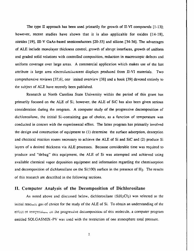
A UHV vacuum system has been designed and assembled for the study of growth
Kinetics of silicon and silicon carbide by the atomic layer epitaxy method. The system has
three chambers: a load lock, a remote hydrogen plasma cleaning chamber, and a desorption
chamber equipped with a shielded mass spectrometer. Labeled schematic drawings of the
latter two chambers are presented in Figures 2 and 3.
4

Reducing flange; quartztube with argon inlet M: 1800 from L: Blank
I F L I
H2 inlet K + Pressure Transducer
Blank
Gate vaManipulator/
Parking Station
Blank Throttle valve;R.A. valve; hose tochemical plasma pump
Gate valve; to diffusion pump
Figure 2. Schematic of hydrogen plasma chamber for removing oxide and free carbon fromsubstrate surfaces prior to loading into thermal desorption chamber.
5
foros foorc13 lam 4Shupigtere
camtbe1 -oe
frandhoe orrog
toumpaing 1chanamcbebe
Gighe vanve: tolv dIfon puugp
aend h.froughupumindgour o
masng tec chachaber
Gate~~~Gt vavelve:fuic pm
Figue 3a Scematc o thefrot ofthetheral esorti o chamernn hamberth
1 31
Line motionfeedthrough witoran
tte lsr or1 ln
Gate~~~Gt vaveaolifuioep;
Fig re b. Sch maic f he ea ofth th em l oro cha be showcaing h pa m en
o etry ortsfrec qimn atshutte L- F6

The top flange of the cleaning chamber (Fig. 2) is equipped with a nominal one inch
quartz tube on which is wound a several turn coil of 0.125 inch copper tubing which is
connected to a radio-frequency (RF) source. The electrical field produced within the qu--"tz
tube by the energized coil causes the rapid movement of any free electrons such that their
collision with Ar molecules introduced into the tube causes ionization which cascades and
results in the generation of a plasma. This plasma will, in turn, be used to excite a hydrogen
plasma from the H2 introduced downstream from the Ar. The sample tc be cleaned is not
immersed in the plasma, thus plasma-induced surface damage is minimized. This method also
does not require high temperatures as most other methods, thus the substrate surface and
the interior doped regions will maintain their initial character.
The mass spectrometer (Fig. 4) ias been configured specially for thermal desorption
studies. It is contained in the main chamber of the desorption system (Fig. 3). This
particular spectrometer is able to monitor the partial pressure of sixteen different species as a
function of both temperature and time. It is equipped with a spectral library of over 70
common gases, thus the species of interest can be isolated in the obtained spectra. For
example, the library spectra of dichlorosilane that was experimentally obtained is shown in
Figure 5 and presented in Table I. Figure 6 also shows the partial pressures of the
dichlorosilane decomposition products obtained as a function of the temperature using our
mass spectrometer.
The desorption chamber also has additional features that will allow us to use the
mass spectrometer in two ways. First, the mass spectrometer chamber has an aperture in
direct line of sight with the sample. By increasing the temperature of the sample and moni-
toring the pressures of the adsorbed molecule (or its decomposit v-. :uct) and all possible
other decomposition products, the temperature at which the adsc e dtoorbs and/or further
decomposes can be identified. This data yields the activation energy necessary for des%,rption
of the major species and subspecies. By analyzing the shape of the desorption curve for
conditions of low coverage, a plot of the desorption rate versus temperature can be obtained.
7

Right angle valve for Blank flangehose to main chamber - !connectto /
/ Fitted closure
ion pump I!K 5.0 - 6.4
Figure 4. Schematic of mass spectrometer chamber (left side) and mass spectrometertube (right side) for thermal desorption system.
PAR;T I AL
T -
4'
07 ,I C, 0
Figure 5. Decomposition spectra of dichlorosilane. See Table I for correlation of gasspecies with mass number.
TABLE I. Correlation of mass numbers determined for the spectra of Figure 5 with actualspecies determined via themal decomposition studies of SiH 2C12.
SPECIES MASS (amul
SiH 2CI 2 101
SiC12H 100SIC12 99SiC1 63.5
I8

xE-11 DCS SPECTRA1** TEMPERATURE 3G
0a5.
103 SiCI H SiI6-C
0 -.. 5Q\,
R/ SiCI 2 H 2 X ', , , S I 2, e \
, \ 55G .u
1. 03 4t7 450.
96.6 I G. 1 . 120. 118.
Tite C seconcs )
Figuie 6. Partial pressures of the SiH 2CI 2 decomposition products shown in the spectraof Figure 5 Pnd Table I.
For the second type of measurements, the mass spectrometer chamber has been
equipped with a fitted closure (see Figure 4) that can be easily raised and lowered for
sampling the random flux of a particular species in the system. This feature, coupled with a
shutter for the sample, allows us to extract quantitative kinetic adsorption information.
Before the introduction of the gas, a spectrum is taken to obtain a baseline measurement of
the speciei of interest. Then, with the shutter covering the sample and the fitted closure
closed, the gas is turned on and a measurement of the background pressure of the introduced
species is taken. The shutter is subsequently moved away from the sample. The
measurement of the decrease in the background signal tells one how much gas has been
9

adsorbed. When the pressure then reaches the original background level, the gas
introduction is terminated. This data yields the adsorption rate and sticking probability
versus the absolute coverage.
The first process to be characterized using the above system will be the epitaxial
deposition of silicon onto a silicon(100) substrate by atomic layer methods. This method is of
great interest for maintaining uniform coverage over a device structure. An important aspect
of ALE growth is its self-limiting nature. After studying all commercially available
silicon-containing species, dichlorosilane was chosen as the best candidate for atomic layer
growth because of the halogen chemistry. The first decomposition product is hydrogen, and
this reaction has an enthalpy of 152 kJ/mol. The remaining chlorines will not be removed
by molecular hydrogen or by other silicon atoms. The result will be the adsorption of one
layer of silicon, terminated by chlorines. The presence of the chlorines will prevent further
adsorption of the silicon species at that site. Once full coverage is achieved, the chlorines can
be removed by the introduction of atomic hydrogen. This reaction has an eT *"alpy of
-452 kJ/mol. The final result is the growth of one atomic layer of silicon.
Once the work on the thermal desorption kinetics of dichlorosilane is completed, the
research will be extended to include a source for depositing carbon via the ALE method.
After examining previous research by Prof. John T. Yates at the University of Pittsburgh on
the adsorption kinetics of various carbon-containing gases, acetylene has been chosen as the
source for carbon. Professor Yates has fully characterized the kinetics of thermal desorption
of various hydrocarbon species .,uch as ethylene, acetylene, propane, and propylene. It was
determined that a double (or triple bond ) between carbons in the source gas was necessary
for adsorption on a silicon surface. The second (or third) bond degenerates to provide the
mechanism for bonding to the surface. Acetylene was chosen over the other gases because it
had the lowest temperature of desorption.
Future equipment development plans include the incorporation of a liquid nitrogen
cooled sample holder. This will allow us to extend the kinetic measurements to temperatures
I ()

less than 300K. We wish to be able to cool the sample without sacrificing the ability to
transfer in fresh samples via the load lock.
IV. Design and Fabrication of Equipment for the Deposition of Si and
SiC Films via ALE
A. Overview
In this program, two different approaches were taken by the Bedair and Davis groups
for the purpose of depositing Si alone (Bedair) or Si and C to reach the ultimate objective of
SiC (Davis). In both groups, the initial objective was the ALE of Si films. The design
philosophies, resulting equipment and the suggested experimental approaches and
precautions derived from these two investigations are described in the following two
subsections.
B. Equipment Design and Development for the Near Atmospheric Pressure Deposition of Si
(Bedair Group)
Overview. The design and construction of the equipment (figure 7) for Si ALE have
been completed and the system is near operational condition. The vacuum integrity of the
system is currently being tested thoroughly prior to connection of the reactant gases. After
this is finished the system will be ready for full operation following a final check of the
pressure, temperature, and flow controls. The main objectives in the equipment design were
high speed deposition, good system integrity for processing control and minimization of
background impurities, and high purity source gases for near atmospheric silicon
Design Philosophy and System Operation. For high speed ALE growth the stage
design depicted in Figure 8 is being used. The reactant gases are dichlorosilane (DCS) and
hydrogen. The rotating sample (see Figure 9) is exposed to only one gas at a time. The
DCS adsorption and decomposition is expected to result in one monolayer of SiCI2 being
chernisorbed, as noted in the previous section. The introduction of molecular hydrogen results
11

,~~ IZ Lqi
I-igure 7. Photograph showing Bcdair's system (without glove box) for ALE of Si andSi/Ge alloys and device structures.
12

Silicon PrecursorsH2 (Si H2 C12, SiH C13, Si2C161..
Extracting Cl Jto form HCI
Substrate
Rotating Part
Fixed Part
Figure 8. Experimental setup for ALE of Si.
~' Susceptar (Growth)
- Exha~ust
--------------- *,----------------- -' Susceptor (Loadin~g)
ruture Lond Lock
Angutar Adjusticilt
Lill Motor
Rotation Motor
Figure 9. Si ALE reaction chamber design.
13

in HCI evolution and a pure Si monolayer left on the substrate surface. Therefore, one
monolayer is deposited per sample revolution.
The chemical system we are using has been explored recently by Nishizawa [35],
though with a different experimental setup. He exposed the substrate to DCS, pumped out
and purged the chamber, and then flowed in the second reactant, hydrogen, to complete the
reaction. The experimental conditions were from about 800 to 900 C at pressures below 1
mTorr. For good surface morphology crystals he was able to obtain growth rates of about
0.03 microns per hour. We are able to operate over the same temperature ranges by using
RF coils to heat the rotating substrate holder, but our technique is better designed for high
speed growth. Since the rotating sample is exposed to only one gas at a time, no purge is
needed between doses which would slow the growth rate. Under optimum growth conditions,
the growth rate is expected to be about 0.2 microns per hour, assuming 2 to 4 seconds per
cycle. To further insure separation of the DCS and hydrogen, inert argon is flowed into the
system to act as a buffer layer between the reactant gas streams. Since there is no need to
evacuate the system between doses, we can also operate at higher pressures. At higher
pressures the flux rate of reactant molecules striking the surface in increased, therefore the
exposure time necessary for one monolayer formation is reduced and the growth rate is again
increased. The pressure in our reaction chamber is controlled by a butterfly valve installed in
the systems exhaust line. This valve is coupled with a pressure gauge to set the system
pressure at any desired level in the I torr to atmospheric pressure range.
The exposure time of the substrate to the reactants is controlled by a stepper motor,
mass flow controllers, and needle valves. The stepper motor is easily programmed to rotate
the sample at a resolution of over 20000 steps per cycle at speeds up to about 40 cycles per
second. The rotational speed may be programmed over each segment of the cycle to
individually control the exposure times of the silicon sample to DCS and hydrogen. Separate
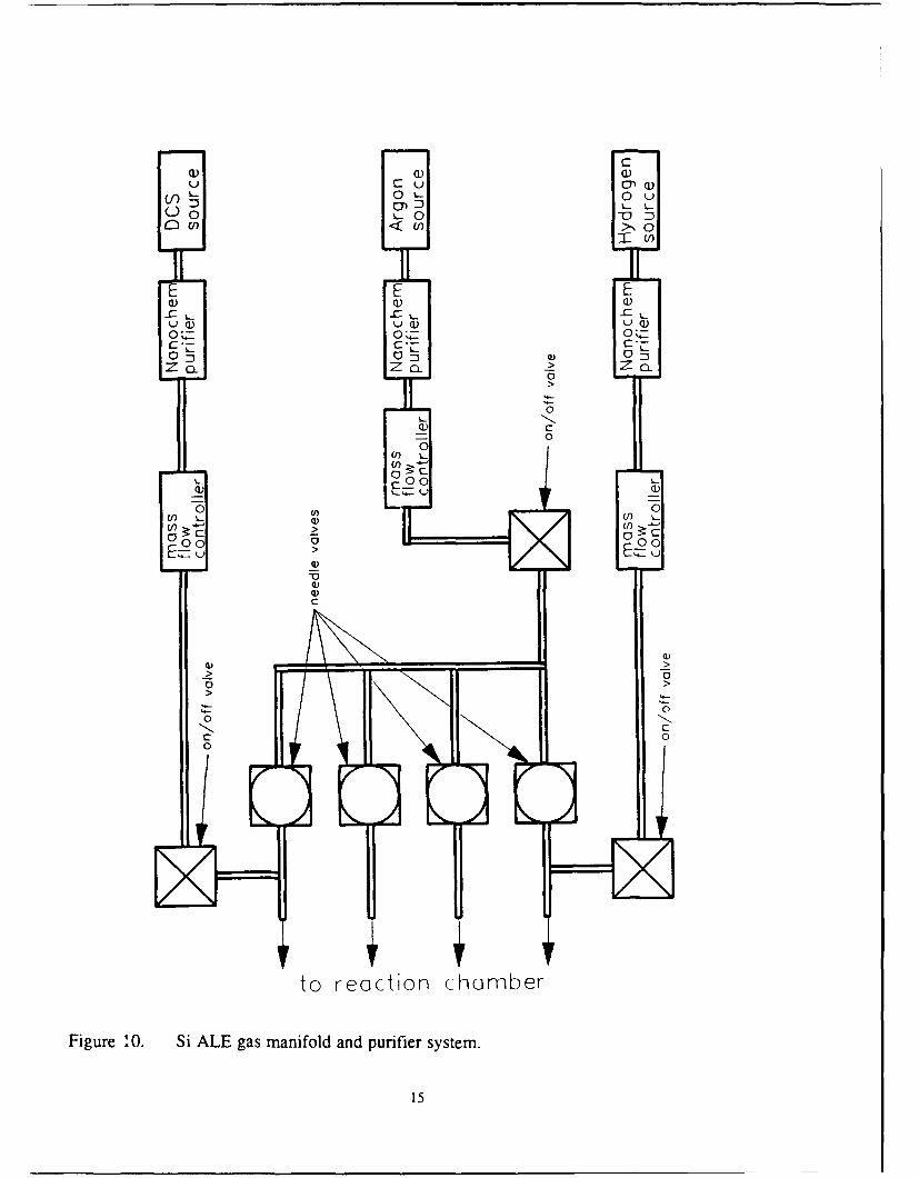
metal seal mass flow controllers have been installed to regulate the total flow of DCS,
hydrogen, and argon into the system, as shown in Figure 10. The maximum flow rates for
14
C On
0 Cu
- Ln
E
Ci) 0 1-)
UU)I IJQ Q
020
Zo.. _0
0 V0
(l L. 4).(
CC
0
to reaction chamber
Figure '.0. Si ALE gas manifold and purifier system.
15

these controllers are 200 sccm, 200 sccm, and 5000 for DCS, hydrogen, and argon
respectively. Needle valves control the dilution of the DCS and hydrogen streams by Ar as
well as the Ar flow rate used to separate the reactant gases. This manifold design is shown
in Figure 10. By adjusting the needle valves and mass flow controllers the total flow rate of
the reactant gas streams may be kept constant while changing the concentrations of the
reactants in the stream. This is desirable to achieve uniform flow profiles across the
substrate surface and still regulate the DCS and hydrogen concentrations. Especially at high
sample rotational speeds and higher pressures, the reactant incident rate on the surface may
otherwise not be uniform without using high flow rates of pure reactants, which may not be
desirable.
Design and Maintenance of System Integrity. The apparatus has been constructed to
minimize the impurity levels, especially water and oxygen, in the system. The reaction
chamber is evacuated to 10- 7 torr and baked out prior to deposition to remove impurities
adsorbed on the walls. The RF coils located outside the quartz chamber are used to heat up
the graphite sample holder for processing as well as for high temperature annealing of the
sample to remove the oxide deposited after ex situ pre-cleaning.
Further precautions have been taken to isolate the reaction system from the
atmosphere and reduce the chances of oxygen and water contamination. The entire
deposition chamber is enclosed in a glove box filled with dry nitrogen. All electrical and
vacuum connections, as well as gas lines, are sealed with O-rings to the walls to prevent
moisture from entering the box. The glove box is kept maintained slightly above atmospheric
pressure by constantly flowing nitrogen into the system and regulating the internal pressure
with a bubbler, which is vented to an exhaust system. For entry and removal of samples and
other necessary equipment into and out of the system an antechamber is attached to the
glove box. The antechamber has an O-ring door to the atmosphere and another one inside of
the glove box. A vacuum line and a line to the glove box itself are connected to the
antechamber. For entry of samples the chamber is pumped out and purged with nitrogen from
16

the box several times in order to remove the atmosphere from the antechamber. At this point
the glove box and antechamber atmospheres are the same and the sample can be brought into
the system for loading into the reaction chamber.
The deposition chamber is shown in Figure 9. The sample is easily loaded and
unloaded via an 0-ring sealed port and raised to the quartz reaction chamber using a
programmable lift motor. The sample holder is heated by RF coils located outside the quartz
chamber and is rotated by simple programming of the rotation motor. Two pumping systems
are employed. One is for baking and purging the system and operates at a base pressure of
10- 7 torr. The pump used for deposition regulates the system pressure and can be set in the
torr to atmospheric range. This pressure control system operates by means of a Baratron
pressure gauge and a butterfly valve. Once the desired pressure is set, the reading from the
pressure gauge is automatically monitored and the butterfly valve adjusted continuously to
increase or decrease the pumping speed and keep the pressure constant.
The system is designed for easy modification for future research. The susceptor
(sample holder) and quartz chamber may be removed for modification if desired. The loading
port can be replaced with a load lock system to further isolate the reaction chamber from the
atmosphere. The gas lines are constructed for addition of dopant sources into the inert argon
lines for doped deposition studies.
Gas Purification. Purifiers have been placed in line with the reactant gases and the
argon. These are Nanochem purifiers which reduce the total impurity levels to the low ppb
concentrations. The purification processes are trade secrets and are based on lithium-phenyl
compounds for hydrogen and on chlorinated compounds for DCS systems. Water and oxygen
contamination are especially harmful to Si epitaxy, due to rapid oxide formation. The
DCS/hydrogen system is selective under many conditions and will not deposit on the oxide.
Therefore, even a minute amount of oxide on the surface can destroy the epitaxial quality.
Sedgwick [401 has recently examined the effects of oxygen and water on the DCS/hydrogen
silicon epitaxial growth system at atmospheric pressure. His studies show that even a
17
99.999% hydrogen source is not pure enough for deposition to occur. As little as 50 ppb of
water and 20 ppb of oxygen can substantially affect growth to allow only polysilicon
deposition. However, using a Nanochem hydrogen purifier, like the type we have installed,
he is able to obtain high quality epitaxial silicon growth.
C. Equipment Design and Development for the Deposition of Si and SiC (Davis Group)
To accomplish the ALE of Si and, ultimately SiC, a special high vacuum system has
been designed and completed. Initially the system is configured to process 1 inch wafers.
Ultimately, the apparatus may be adapted to handle samples up to 2 inches in diameter. The
system consists of three chambers; a load lock, a cleaning chamber, and a growth chamber. A
composite schematic drawing of the system is shown in Figure 11 and a photograph of the
chambers and operations cabinet in Figure 12. The system is made from suiinless steel with
knife edge seals. Process gases are reguldLec by thermal mass flow controllers. Process
pnmping is handled by a rotary vane pump. High vacuum is achieved through diffusion pumps.
The load lock is a simple five way cross that can hold up to four samples. All samples
are introduced to and removed from the system through this chamber. In the present design,
the load lock may be evacuated to the millitorr level.
After passing through the load lock, the samples are cleaned using a remote hydrogen
plasma in a chamber specially designed for this purpose. The cleaning chamber is pumped by
a diffusion pump to high vacuum, and the process gas is removed from the chamber by a
rotary vane pump through a throttle valve. To assure identical sample cleaning within a run,
up to four samples may be simultaneously cleaned in the chamber. In current silicon
technology, many different plasma cleaning routes are employed through varying flow rates,
substrate temperatures, plasma power, and process pressure. This chamber and its
associated power supply is also capable of performing many variations on the plasma
cleaning operation.
After cleaning, the samples are transferred to the growth chamber. Like the cleaning
chamber, the growth chamber is pumped to high vacuum using a diffusion pump, and the
18

U
Atomic Layer Epitaxy System
load LookDiffusion
Pump *
0**
E* S
a Cleaning
Growth ChamberTop Me Right Side View
Figure 11. Schematic of Entire ALE growth chamber and associated cleaning chamber andlode lock used by Davis and coworkers for the ALE of Si, SiC and devicestructures from these two materials.
19

I
Figure 12. Photograph of completed ALE deposition system used by Davis and coworkersof the ALE of Si, SiC and device structures from these two materials.
product and residual process gases are removed through the throttle valve using a rotary
vane pump. Inside the growth chamber, the samples and their travelers are mounted on a
revolving, receiver stage above the heater body that will introduce them to as many as eight
independent gas fluxes distributed by the vane assembly. A schematic of this growth
assembly is shown in cross section in Figure 13. The vane assembly is divided into 16
sections, each supplying a different gas. Thus, as a sample rotates below the vane assemblyit will see in turn: Ar-SiH2CI2-Ar -H2 ... etc. repeated 4 times per revolution. The heater
design allows heating of the samples as hig(h0 as 100° C, however the present intent is to
ascertain process routes which will allow the deposition of both Si and SiC at substantially
lower temperatures.
Due to the large mass that will be heated inside the growth chamber. and the
possibility for high temperatures. appropriate heat shielding. and a water cooled chamber are
employed.
20

___N__ Vane Assembly '
Sreler Sample Receiver
Power Leads
- SiC Coated Graphite 316 Stainless Steel
L-' Alumina Water Cooled CavityFigure 13. Cross-sectional view of the ALE growth assembly for the deposition of Si and
SiC.
The system described above has been completed and commissioned. The cleaning
chamber reaches a base of < 3 X 10⁻⁸ torr, and the growth chamber has been evacuated to
< 3 X 10⁻⁹ torr after an appropriate bakeout. Four cleaned samples can be loaded into the
system and be under a 10-7 vacuum in less than 10 minutes. The heaters in the cleaning and
the growth chambers have achieved sample temperatures of 500'C and 960*C, respectively.
Based on the studies with SOLGASMIX-PV discussed in the Section II and other
limiting factors, the following initial experimental growth parameters were selected:
Pressure: 1 torr
Temperature: 6000C to 7000C
Gas Flow ratio: I Ar: 1 SiH 2CI2:1 H2
Rotation speed: 20 rpm
To determine the thickness of the ALE films, Secondary Ion Mass Spectroscopy
(SIMS) will be employed. For this, heavily As-doped Si(100) wafers (n=10 19) were used. It
is known that at these temperatures, arsenic is not mobile. Given the sensitivity of SIMS for
As with the use of a Cs primary ion beam, it is possible to sputter the samples until As is
detected. Then using a profilometer, one can determine the depth of the sputtered pit, and
hence the film thickness. For our equipment, the optimal film thickness is around 500
21

angstroms. Since ALE would not necessarily grow a complete monolayer per cycle, a target
thickness of 750 angstroms was sought.
For this run, four samples were processed in the following manner:
• Modified RCA clean
" Remote Hydrogen plasma clean
" ALE growth of 750 angstroms (560 cycles = 760 angstroms)
The details of each of these steps is shown in Table II.
TABLE II. The details of each of the process steps used to prepare the Si(100)wafers anid load them in the growth chamber prior to the ALE of Si.
1. Modified RCA clean:* 5 minutes in 60'C H2SO4* D.I. water rinse* 5 minutes in 60'C NH 4OH + H20 2
* D.I. water rinse* 5 minutes in B,.uffered Oxide Etch* D.I. water rinse
2. Load samples into load lock, transfer to cleaning ct-amber.
3. Remote hydrogen plasma clean:* Heat samples to 310'C" Admit Ar at 90 sccm* Admit H2 at 15 sccm" Pressure at 300 mtorr" RF power 35 watts* 30 minutes* Heatej off, let cool to 250'C" RF power off* Gases off, evacuate to high vacuum
4. Transfer samples to growth chamber:" Heat samples to 620'C" Ar at 104 sccm" H2 at 52 sccm" SiCI2H2 at 52 sccm" Pressure at 1 ton" Rotate 20 rpm for 140 rotations• Gases off, heater off" Evacuate to high vacuum

The samples are subsequently angle lapped on a 17' holder with 1 micron diamond
paste, and polished for 20 minutes with Syton® solution to dtermine the presence of a film in
a manner shown in Figure 14 below. At 620'C, no growth of Si was observed.
Deposited Film
Substrate
Figure 14. Schematic of angle lapped sample showing the magnification effect on thedeposited film and its thickness.
Much additicnal research will be conducted to fully comprehend the details of the
reactions ongoing in the growth chamber. These results will be correlated with those derived
from the thermal desorpzion studies described abeve.
V. ALE of Silicon Using a Chemical Vapor Deposition System
One of the co-principal investigators of this proposal has also demonstrared ALE oi
Si using alternate flows of SiH2C12 and H2 at 815 0C and an As-doped Si substrate. Briefly,
As profiles were obtained from the bare substrate (Fig. 15) and witb the substrate exposed
only to SiH2C12 for 30 minutes (Fig. 16). As shown in Figure 16, onl = 0.01 Itm of Si was
deposited (the profile from 0.01-0.03 ;.im shows the beam is already overlapping the Si
substrate-as diffusion into the growing film was not detected). By contrast, the alternate
introduction of SiH2CI2 and H2 under the conditions and for the times shown in Figures 17
and 18 strongly indicate that the SiH2CI2 is decomposing to a precursor species (presumably
SiCI2) which is chemisorbing to the surface of the Si substrate and subsequently reacting
with the introduced H-2 to produce deposition of Si. Some of the SiH2C12 also decomposed
23

At/Cmn3 Bulk doped As
1 E20:
1E19
1E18:Substrate: As-doped(2 x 10¹⁹/CM3) Si
SIMS Profile: As
No Deposition or Exposure to SiH2CI2
1E17 1_ _ _ _ _ _ _ _ _ _ _ _ _ _ _ _ _ _ _ _ _ _ _ _ _ _ _ _
0.06 .12 .18 .24 .3
Depth (M iorometer.w)
Figure 15. Secondary ion mass spectrometry profile of As-doped Si substrate used for SALE research.
24

At/Cm3 Sample 1
1 E20
1E19
Conditions and Results of Deposition
* Substrate: As-doped (2 x 10¹⁹/cm 3) Si1E 18 SIMS Profile: As
• Temperature: 815"C• Gas: SiH2CI2* Pressure: 4 mTorr• Flow Time: 1800 s* Depth of Si: .15nm* Final Surface Condition: Excellent
1E17 I I12 .18 .24 .3
Depth (M i rometor-o)
Figure 16. SIMS piofile of As showing slight deposition of Si from 0 - 0.01 microns fromdecomposition of SiH2Cl 2 at 815'C on an As-doped Si substrate.
25

Conditions and Results of Deposition
" Substrate: As-doped (2 x 10¹⁹/cm 3) Si" SIMS Profile: As"Temperature: 815*C
Atcs Gases: SiH2CI2 Vacuum H2 VacuumTime imem3
*Total Press. 4 mTorr 1200 mTorI E20 *Flow Time 60 s 40 s 15 s 150 s
*# of cycles 30 30 30 30*bDepth of -145nmDeposited Si
-Surface Condition: Excellent
1E191
lEie
IE17 I0.06 .12 .18 .24 Is
Depth (Mi ~ottr-e)
Figure 17. SIMS profile of As showing deposition of ca. 0.14 microns of Si by atomic layerepitaxy via the alternate introduction of SiH-2C12 and H2 under the conditionsshown in the table in the figure.
26

Conditions and Results of Deposition
" Substrate: As-doped (2 x 10¹⁹/cm3) Si" SIMS Profile: As" Temperature: 815*C
At/Cm3 Gases: SiH2CI2 Vacuum H2 Vacuun-Tie Time(5
1E201 -,Total Press. 4 mTorr 400 mTorr-Flow Time 60s 40 s 15 s 100 s-# *of cycles 100 100 100 100-Depth of -200 nmDeposited Si
-Surface Condition: Excellent
1E191
1E16
E17 .12 .1s .24 .3
Depth (Miorcmotere)
Figure 18. SIMS profile of As showing deposition of ca. 0.20 microns of Si by atomic layerepitaxy via the alternate introduction of SiH2Cl 2 and H2 under the conditionsshown in the table in the figure.
27

on its own, as the initial exposure without H2 resulted in = 50 unit cells of Si while the 30
alternate exposures produced 400 unit cells and the 100 alternate exposures (with shorter
exposures to H2) resulted in = 450 unit cells. It is believed that some of the SiH2C12 is not
being pumped .',.y i.- the ihitcrvcaiing ,.-acuatioai. This is ind.icated by the proportionaly
smaller thickness of Si when the pumping time increased from 30s to 100s. Reducing the
temperature to 770'C did not result in the deposition of Si under any conditions.
VI. Summary
The primary focus of the research for this grant has been the atomic layer epitaxy of
Si; however, the ALE of SiC has also received serious consideration. A computer assisted
study, based on the free energy minimization of a thermodynamic system undergoing
equilibrium reactions has shown that the progressive decomposition of SiH 2 Cl2 (the Si
precursor of choice in this study) results in the products of SiC12 , H2 , SiH 2C12 , HC1 and Si.
Moreover, above 600'C, SiC12 is stable. Thus SiCI2 adsorbed onto the surface will not
decompose. It is predicted to react with H2, forming Si on the surface. The experimental
program has primarily involved the design and fabrication of equipment to (1) determine the
surface adsorption, desorption and chemical reaction routes necessary to achieve the ALE of
Si and SiC and (2) produce Si layers of a desired thickness via ALE processes. The ALE of
Si was achieved at 815'C using available chemical vapor deposition equipment and
information regarding the chemisorption and decomposition of dichlorosilane on the Si(100)
surface in the presence of H2 . Reducing the temperature to 770'C did not result in the
deposition of Si under any conditions of flow rate or total pressure.
All growth systems are now operational. The future research will be devoted to the
ALE of Si and C as it pertains to the growth of SiC as well as the ALE of diamond and CeO2.
Studies will examine the effects of temperature, pressure, and rotational speed on film quality
and coverage per cycle. The results of the thermal desorption studies will be invaluable in
selecting the correct starting gas species and the temperature and pressure regimes wherein
ALE of these materials can be achieved. The films will be analyzed by SIMS, TEM, SEM
28

and optical microscopy. It should also be noted that the ALE of gallium nitride and aluminum
nitride will be addressed. Finally the growth of some of these materials (e.g., SiC) by ALE
within a Si(100) trench will be studied.
VII. References
1. T. Suntola and J. Antson, U.S. Patent 4,058,430 (1977).
2. M. Ahonen, M. Pessa and T. Suntola, Thin Solid Films, 65, 301 (1980).
3. M. Pessa, R. Makela, and T. Suntola, Appl. Phys. Lett., 38, 131 (1981).
4. T. Yao and T. Takeda, Appl. Phys. Let., 48, 160 (1986).
5. T. Yao, T. Takeda, and T. Watanuki, Appl. Phys. Lett., 48, 1615 (1986).
6. T. Yao, Jpn. J. Appl. Phys., 25, L544 (1986).
7. T. Yao and T. Takeda, J. Cryst. Growth, 81, 43 (1987).
8. M. Pessa, P. Huttunen and M.A. Herman, J. Appl. Phys., 54, 6047 (1983).
9. C.H.L. Goodman and M.V. Pessa, J. Appl. Phys., 60, R65 (1986).
10. M.A. Herman, M. Valli and M. Pessa, J. Cryst. Growth, 73, 403 (1985).
11. V.P. Tanninen, M. Oikkonen and T. Tuomi, Phys. Status Solidi, A67, 573 (1981).
12. V.P. Tanninen, M. Oikkonen and T. Tuomi, Thin Solid Films, 90, 283 (1983).
13. D. Theis, H. Oppolzer, G. Etchinghaus and S. Schild, J. Cryst. Growth, 63, 47 (1983).
14. S. Lin, J. Electrochm. Soc., 122, 1405 (1975).
15. H. Antson, M. Leskela, L. Niinisto, E. Nykanen and M. Tammenmaa, Kem.-Kemi, 12,11 (1985).
16. R. Tornqvist, Ref. 57 in the bibliography of Chapt. 1 of Ref. 39 of this proposal.
17. M. Ylilammi, M. Sc. Thesis, Helsinki Univ. of Technology, Espoo (1979).
18. L. Hiltunen, M. Leskela, M. Makela, L. Niinisto, E. Nykanen and P. Soininen, SurfaceCoatings and Technology, in press.
19. 1. Suni, Ref. 66 in the bibliography of Chapt. 1 of Ref. 39 of this proposal.
29

20. S.M. Bedair, M.A. Tischler, T. Katsuyama and N.A. El-Masry, App!. Phys. Lett., 47,
51 (1985).
21. M.A. Tischler and S.M. Bedair, 48, 1681 (1986).
22. M.A. Tischler and S.M. Bedair, . Cryst. Growth, 77, 89 (1986).
23. M.A. Tischler, N.G. Anderson and S.M. Bedair, App!. Phys. Lett., 49, 1199 (1986).
24. M.A. Tischier, N.G. Anderson, R.M. Kolbas and S.M. Bedair, App!. Phys. Lett., 50,1266 (1987).
25. B.T. McDermott, N.A. El-Masry, M.A. Tischler and S.M.Bedair, App!. Phys. Lett., 51,1830 (1987).
26. M.A. Tischler, N.G. Anderson, R.M. Kolbas and S.M. Bedair, SPIE Growth Comp.Semicond., 796, 170 (1987).
27. S.M. Bedair in Compound Semiconductor Growth Processing and Devices for the1 990's, Gainesville, FL, 137 (1987).
28. J. Nishizawa, H. Abe and T. Kurabayashi, J. Electrochem. Soc., 132, 1197 (1985).
29. M. Nishizawa, T. Kurabayashi, H. Abe, and N. Sakurai, J. Electrochm. Soc., 134, 945(1987).
30. P.D. Dapkus in Ref. 27, p. 95.
31. S.P. Denbaars, C.A. Beyler, A. Hariz and P.D. Dapkus, App!. Phys. Lett., 51, 1530(1987).
32. M. Razeghi, Ph. Maurel, F. Omnes and J. Nagle, App!. Phys. Lett., 51, 2216 (1987).
33. M. Ozeki, K. Mochizuki, N. Ohtsuka and K. Kodama, J. Vac. Sci. Technol. B5, 1184(1987).1
34. Y. Suda, D. Lubben, T. Motooka and J. Greene, J. Vac. Sci. Technol., B7, 1171 (1989).
35. J. Nishizawa, K. Aoki, S. Suzuki and K. Kikuchi, J. Cryst. Growth, 99, 502 (1990).
36. T. Tanaka, T. Fukuda, Y. Nagasawa, S. Miyazaki and M. Hirose, App!. Phys. Lett.,56, 1445 (1990).
37. T. Suntola and J. Hyvarinen, Ann. Rev. Mater. Sci., 25, 177 (1985).
38. M. Simpson and P. Smith, Chem. Brit., 23, 37 (1987).
39. T. Suntola and M. Simpson, Atomic Layer Epitaxy, Chapman and Hall, New York,1990.
40. T. Sedgwick, M. Berkenblit, App!. Phys. Lett. 54(26), 26 June 1989, pp. 2689-269 1.
30


![Wide-Bandga 16.Wide-BandgapII-VISemiconductors ... · molecular-beam epitaxy (MBE) [16.3], metalorganic molecular-beam epitaxy (MOMBE) [16.4] and atomic-layer epitaxy (ALE) [16.5]](https://img.pdfslide.us/doc/110x75/5e1f371b74bffa7fb71fc624/wide-bandga-16wide-bandgapii-visemiconductors-molecular-beam-epitaxy-mbe.jpg)