Embed Size (px)
Citation preview
SANDIA REPORT SAND2009-6130 Unlimited Release Printed September 2009
Final LDRD Report: Nanoengineering for Solid-State Lighting Mary H. Crawford, Arthur J. Fischer, Daniel D. Koleske, Stephen R. Lee, Nancy A. Missert, E. Fred Schubert, Christian Wetzel, Shawn-Yu Lin Prepared by Sandia National Laboratories Albuquerque, New Mexico 87185 and Livermore, California 94550
Sandia is a multiprogram laboratory operated by Sandia Corporation, a Lockheed Martin Company, for the United States Department of Energy’s National Nuclear Security Administration under Contract DE-AC04-94AL85000.
Approved for public release; further dissemination unlimited.
2
Issued by Sandia National Laboratories, operated for the United States Department of Energy by Sandia Corporation. NOTICE: This report was prepared as an account of work sponsored by an agency of the United States Government. Neither the United States Government, nor any agency thereof, nor any of their employees, nor any of their contractors, subcontractors, or their employees, make any warranty, express or implied, or assume any legal liability or responsibility for the accuracy, completeness, or usefulness of any information, apparatus, product, or process disclosed, or represent that its use would not infringe privately owned rights. Reference herein to any specific commercial product, process, or service by trade name, trademark, manufacturer, or otherwise, does not necessarily constitute or imply its endorsement, recommendation, or favoring by the United States Government, any agency thereof, or any of their contractors or subcontractors. The views and opinions expressed herein do not necessarily state or reflect those of the United States Government, any agency thereof, or any of their contractors. Printed in the United States of America. This report has been reproduced directly from the best available copy. Available to DOE and DOE contractors from U.S. Department of Energy Office of Scientific and Technical Information P.O. Box 62 Oak Ridge, TN 37831 Telephone: (865) 576-8401 Facsimile: (865) 576-5728 E-Mail: [email protected] Online ordering: http://www.osti.gov/bridge Available to the public from U.S. Department of Commerce National Technical Information Service 5285 Port Royal Rd. Springfield, VA 22161 Telephone: (800) 553-6847 Facsimile: (703) 605-6900 E-Mail: [email protected] Online order: http://www.ntis.gov/help/ordermethods.asp?loc=7-4-0#online
3
SAND2009-6130 Unlimited Release
Printed September 2009
Nanoengineering for Solid-State Lighting
Mary H. Crawford, Arthur J. Fischer, Stephen R. Lee Semiconductor Material and Device Sciences Department
Sandia National Laboratories P.O. Box 5800
Albuquerque, New Mexico 87185-MS1086
Daniel D. Koleske Advanced Materials Sciences Department
Sandia National Laboratories P.O. Box 5800
Albuquerque, New Mexico 87185-MS1086
Nancy A. Missert Nanomaterials Sciences Department
Sandia National Laboratories P.O. Box 5800
Albuquerque, New Mexico 87185-MS1415
E. Fred Schuberta, Christian Wetzelb, Shawn-Yu Linb Future Chips Constellation
aDepartment of ECSE and Department of Physics bDepartment of Physics
Rensselaer Polytechnic Institute 110 Eighth Street Troy, NY 12180
Abstract
This report summarizes results from a 3-year Laboratory Directed Research and Development project performed in collaboration with researchers at Rensselaer Polytechnic Institute. Our collaborative effort was supported by Sandia’s National Institute for Nanoengineering and focused on the study and application of nanoscience and nanoengineering concepts to improve the efficiency of semiconductor light-emitting diodes for solid-state lighting applications. The project explored LED efficiency advances with two primary thrusts: (1) the study of nanoscale InGaN materials properties, particularly nanoscale crystalline defects, and their impact on internal quantum efficiency, and (2) nanoscale engineering of dielectric and metal materials and integration with LED heterostructures for enhanced light extraction efficiency.
4
ACKNOWLEDGMENTS The authors gratefully acknowledge technical contributions from M. A. Banas, K. H. A. Bogart, D. M. Follstaedt, G. Thaler, K. C. Cross, K. R. Westlake, K. W. Fullmer, A. J. Coley, R. G. Copeland, M. L. Smith, J. M. Kempisty, J. K. Kim, F. W. Mont, M. F. Schubert, Q. Dai, D. Zhu, S. Chhajed, A. N. Noemaun, J. Xu, Y. Xia, M.-F. Chen and Y.-S. Kim. Management support from Dan Barton (project manager), Bob Biefeld and Jerry Simmons is also greatly appreciated. We also thank Regan Stinnett, Justine Johannes, Duane Dimos and Rick Stulen for their support and encouragement in NINE program activities.
5
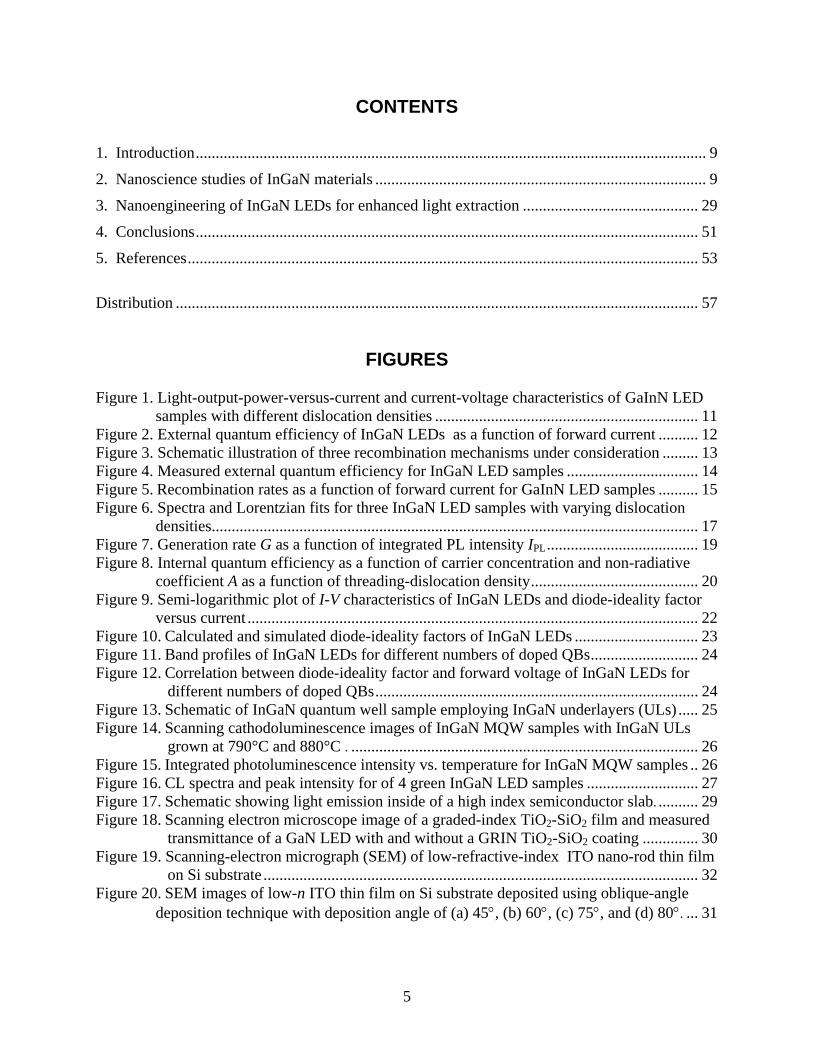
CONTENTS
1. Introduction ................................................................................................................................ 9
2. Nanoscience studies of InGaN materials ................................................................................... 9
3. Nanoengineering of InGaN LEDs for enhanced light extraction ............................................ 29
4. Conclusions .............................................................................................................................. 51
5. References ................................................................................................................................ 53
Distribution ................................................................................................................................... 57
FIGURES Figure 1. Light-output-power-versus-current and current-voltage characteristics of GaInN LED
samples with different dislocation densities .................................................................. 11 Figure 2. External quantum efficiency of InGaN LEDs as a function of forward current .......... 12 Figure 3. Schematic illustration of three recombination mechanisms under consideration ......... 13 Figure 4. Measured external quantum efficiency for InGaN LED samples ................................. 14 Figure 5. Recombination rates as a function of forward current for GaInN LED samples .......... 15 Figure 6. Spectra and Lorentzian fits for three InGaN LED samples with varying dislocation
densities.......................................................................................................................... 17 Figure 7. Generation rate G as a function of integrated PL intensity IPL ...................................... 19 Figure 8. Internal quantum efficiency as a function of carrier concentration and non-radiative
coefficient A as a function of threading-dislocation density .......................................... 20 Figure 9. Semi-logarithmic plot of I-V characteristics of InGaN LEDs and diode-ideality factor
versus current ................................................................................................................. 22 Figure 10. Calculated and simulated diode-ideality factors of InGaN LEDs ............................... 23 Figure 11. Band profiles of InGaN LEDs for different numbers of doped QBs ........................... 24 Figure 12. Correlation between diode-ideality factor and forward voltage of InGaN LEDs for
different numbers of doped QBs ................................................................................. 24 Figure 13. Schematic of InGaN quantum well sample employing InGaN underlayers (ULs) ..... 25 Figure 14. Scanning cathodoluminescence images of InGaN MQW samples with InGaN ULs
grown at 790°C and 880°C . ....................................................................................... 26 Figure 15. Integrated photoluminescence intensity vs. temperature for InGaN MQW samples .. 26 Figure 16. CL spectra and peak intensity for of 4 green InGaN LED samples ............................ 27 Figure 17. Schematic showing light emission inside of a high index semiconductor slab. .......... 29 Figure 18. Scanning electron microscope image of a graded-index TiO2-SiO2 film and measured
transmittance of a GaN LED with and without a GRIN TiO2-SiO2 coating .............. 30 Figure 19. Scanning-electron micrograph (SEM) of low-refractive-index ITO nano-rod thin film
on Si substrate ............................................................................................................. 32 Figure 20. SEM images of low-n ITO thin film on Si substrate deposited using oblique-angle
deposition technique with deposition angle of (a) 45, (b) 60, (c) 75, and (d) 80. ... 31
6
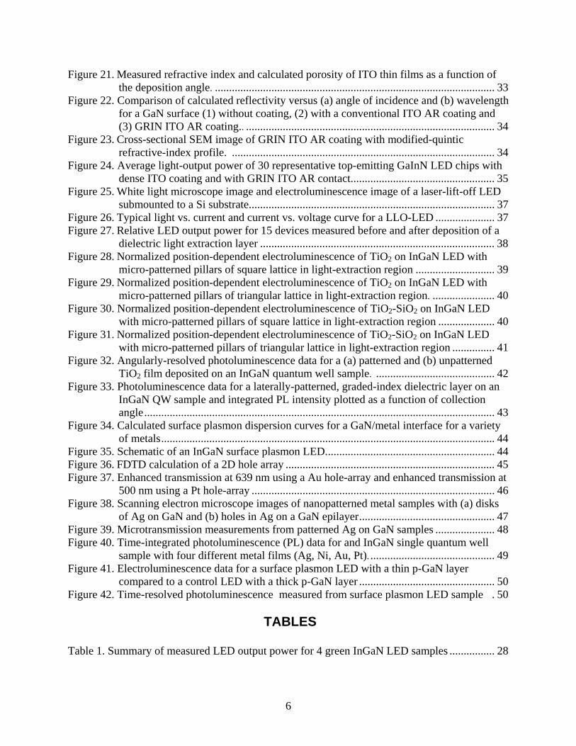
Figure 21. Measured refractive index and calculated porosity of ITO thin films as a function of the deposition angle. ................................................................................................... 33
Figure 22. Comparison of calculated reflectivity versus (a) angle of incidence and (b) wavelength for a GaN surface (1) without coating, (2) with a conventional ITO AR coating and (3) GRIN ITO AR coating.. ........................................................................................ 34
Figure 23. Cross-sectional SEM image of GRIN ITO AR coating with modified-quintic refractive-index profile. ............................................................................................. 34
Figure 24. Average light-output power of 30 representative top-emitting GaInN LED chips with dense ITO coating and with GRIN ITO AR contact. .................................................. 35
Figure 25. White light microscope image and electroluminescence image of a laser-lift-off LED submounted to a Si substrate....................................................................................... 37
Figure 26. Typical light vs. current and current vs. voltage curve for a LLO-LED ..................... 37 Figure 27. Relative LED output power for 15 devices measured before and after deposition of a
dielectric light extraction layer ................................................................................... 38 Figure 28. Normalized position-dependent electroluminescence of TiO2 on InGaN LED with
micro-patterned pillars of square lattice in light-extraction region ............................ 39 Figure 29. Normalized position-dependent electroluminescence of TiO2 on InGaN LED with
micro-patterned pillars of triangular lattice in light-extraction region. ...................... 40 Figure 30. Normalized position-dependent electroluminescence of TiO2-SiO2 on InGaN LED
with micro-patterned pillars of square lattice in light-extraction region .................... 40 Figure 31. Normalized position-dependent electroluminescence of TiO2-SiO2 on InGaN LED
with micro-patterned pillars of triangular lattice in light-extraction region ............... 41 Figure 32. Angularly-resolved photoluminescence data for a (a) patterned and (b) unpatterned
TiO2 film deposited on an InGaN quantum well sample. .......................................... 42 Figure 33. Photoluminescence data for a laterally-patterned, graded-index dielectric layer on an
InGaN QW sample and integrated PL intensity plotted as a function of collection angle ............................................................................................................................ 43
Figure 34. Calculated surface plasmon dispersion curves for a GaN/metal interface for a variety of metals ...................................................................................................................... 44
Figure 35. Schematic of an InGaN surface plasmon LED. ........................................................... 44 Figure 36. FDTD calculation of a 2D hole array .......................................................................... 45 Figure 37. Enhanced transmission at 639 nm using a Au hole-array and enhanced transmission at
500 nm using a Pt hole-array ...................................................................................... 46 Figure 38. Scanning electron microscope images of nanopatterned metal samples with (a) disks
of Ag on GaN and (b) holes in Ag on a GaN epilayer ................................................ 47 Figure 39. Microtransmission measurements from patterned Ag on GaN samples ..................... 48 Figure 40. Time-integrated photoluminescence (PL) data for and InGaN single quantum well
sample with four different metal films (Ag, Ni, Au, Pt). ............................................ 49 Figure 41. Electroluminescence data for a surface plasmon LED with a thin p-GaN layer
compared to a control LED with a thick p-GaN layer ................................................ 50 Figure 42. Time-resolved photoluminescence measured from surface plasmon LED sample . 50
TABLES
Table 1. Summary of measured LED output power for 4 green InGaN LED samples ................ 28

7
NOMENCLATURE AFM Atomic force microscopy AR Anti-reflection CL Cathodoluminescence DBR Distributed Bragg reflector EBL Electron block layer EL Electroluminescence EQE External quantum efficiency FDTD Finite-difference time-domain GRIN Graded refractive index IQE Internal quantum efficiency ITO Indium tin oxide LDRD Laboratory Directed Research and Development LI Light output vs. current LED Light-emitting diode LLO Laser lift-off MOVPE Metal-organic vapor phase epitaxy MQW Multi-quantum well NINE National Institute for Nanoengineering PhC Photonic crystal PL Photoluminescence QB Quantum barrier QW Quantum well RPI Rensselaer Polytechnic Institute SNL Sandia National Laboratories TE Transverse electric TM Transverse magnetic SSL Solid-state lighting TRPL Time-resolved photoluminescence UL Underlayer XRD X-ray diffraction

8
9
1. Introduction
Solid state lighting (SSL) based on semiconductor light-emitting diodes (LEDs) has the potential to have a dramatic global impact. If LED electrical-to-optical energy conversion efficiency goals of 50% or greater can be achieved, worldwide electricity consumption due to lighting could be decreased by more than 50%, and total consumption of electricity could be decreased by more than 10%. Yet, to realize this future benefit, we must overcome significant technical challenges. The most fundamental challenges involve understanding the nanoscale science that governs light generation and extraction from visible LED semiconductor materials and developing nanoscale engineering concepts to achieve the significant increases in LED optical efficiency that are required to make SSL a reality.
This report is an overview of work done in a 3-year LDRD project entitled “Nanoengineering for Solid-State Lighting”. The project was supported by Sandia’s National Institute for Nanoengineering (NINE) program and had a primary goal of exploring both nanoscience and nanoengineering approaches to improving LED efficiency for SSL applications. The work was done in close collaboration with the groups of Professor E. Fred Schubert, Professor Christian Wetzel and Professor Shawn-Yu Lin at Rensselaer Polytechnic Institute (RPI). Our collaborative effort focused on developing and applying innovative concepts to achieve energy efficient SSL by enhancing optical efficiency of LED materials in two primary ways: (1) study and manipulation of nanoscale InGaN materials properties, and particularly nanoscale crystalline defects, to fundamentally improve internal quantum efficiency of light emitting materials, and (2) nanoscale engineering of dielectric and metallic materials and integration with LED heterostructures for enhanced light extraction. In the following sections we outline advances we have made in each of these thrust areas.
2. Nanoscience studies of InGaN materials A major roadblock to the realization of energy efficient SSL is the limited internal quantum efficiency (IQE) of InGaN-based visible LEDs. While violet and blue LEDs have been shown to have IQE of ~70 % at low current densities [2], LED efficiency is greatly reduced at longer (green) wavelengths and under high current density operation (so-called “efficiency droop”). Previous studies have revealed that InGaN alloys are dominated by a range of nanoscale materials properties and phenomena that play a crucial role in the light emission process. Our efforts in this program have had an emphasis on examining the influence of extended crystalline defects (e.g., threading dislocations and “v-defects”) on carrier recombination processes and IQE of InGaN structures. In the following subsections, we present several studies that examine various ways in which extended defects and heterostructure design of InGaN quantum wells (QWs) impact IQE. Given that efficiency droop at high current densities is a critical roadblock to high power, high efficiency SSL, our first topic focuses on examining the impact of threading dislocations on efficiency droop of InGaN LEDs. In subsection 2.2, we further apply photoluminescence (PL) studies of InGaN LEDs to quantify both the IQE vs. carrier density relationship and the non-radiative coefficient A as a function of dislocation density. In our studies of efficiency droop, we discovered that particular InGaN QW heterostructure designs enabled significantly reduced voltages and ideality factors in InGaN LEDs. In
10
particular, n-type doping of GaN barrier layers in the InGaN MQW active region had a strong impact on these device parameters and our investigation of that phenomenon is presented in subsection 2.3. Finally, in subtopic 2.4, we shift emphasis to another type of common extended defect in InGaN: hexagonal pit defects (so-called “v-defects”) that are particularly prevalent in green and longer wavelength InGaN QW structures. Our studies of these defects include both an approach to controllably nucleate v-defects by employing low-growth-temperature InGaN epilayers (“underlayers”) beneath QW layers as well as PL, cathodoluminescence (CL), and electroluminescence (EL) studies of the impact of underlayers and v-defects on InGaN IQE. 2.1 The impact of Threading Dislocations on Efficiency Droop of
InGaN LEDs1
The efficiency droop, prominent in GaInN-based light-emitting pn-junction devices, is the gradual decrease of the power efficiency as the injection current increases. This phenomenon is a severe problem affecting predominantly high-power light-emitting diodes (LEDs) and semiconductor injection lasers, both of which operate at inherently high current densities. Understanding and mitigating efficiency droop is especially critical to attaining viable LEDs for solid-state lighting applications.
The efficiency droop results from a non-radiative carrier loss mechanism that has little relevance at low forward currents but becomes larger as the current increases. Several explanations for efficiency droop have been proposed, including carrier leakage at high forward currents [2-4] – and recently, Auger recombination [5]. Junction heating [6] and carrier delocalization from In-rich low-defect-density regions at high carrier densities [7, 8] have also been suggested as explanations for this effect. In addition, it has been shown that the reduced dislocation density attainable for growth on GaN bulk substrates (compared with sapphire substrates) can influence the magnitude efficiency droop [9].
In this work, we seek to clarify the efficiency droop mechanism by analyzing the light output of GaInN LEDs with a rate equation model that allows us to determine the relative radiative and nonradiative recombination rates, as well as the additional carrier loss term that produces the droop at high currents. We examine the effect of dislocation density on efficiency droop through the evaluation of GaInN LEDs grown on GaN-on-sapphire templates with low and high threading dislocation densities (5.3 108 cm–2 and 5.7 109 cm–2). We compare the characteristics of the three recombination terms for LEDs on these two templates – with a particular focus on the droop-inducing carrier-loss mechanism – as a function of forward current. This approach enables us to characterize the competition between recombination mechanisms in GaInN LEDs as a function of forward current and dislocation density, providing direct insight into the nature of the carrier loss mechanism that dominates in the high current regime.
The GaInN LEDs used in this study are grown on c-plane sapphire using metal-organic chemical vapor deposition in a Veeco D-125 reactor. Threading dislocation densities in the GaN templates used for LED growths are controlled by varying nucleation-layer-growth and film-coalescence parameters [10, 11] and are verified after growth using x-ray diffraction [12]. For consistency, LED structures are concurrently grown in a subsequent growth run using n-type
1 This work was published in Applied Physics Letters and may be found at http://link.aip.org/link/?apl/91/231114. Copyright 2007 American Institute of Physics.
11
GaN-on-sapphire templates with different dislocation densities. The LED heterostructure is characterized by x-ray diffraction (XRD) and in-situ optical reflectance [13] and consists of five 2.4-nm-thick Ga0.87In0.13N quantum wells sandwiched between 7.5-nm-thick Si-doped GaN barriers followed by a 30-nm-thick p-type Al0.15Ga0.85N electron-block layer and a 400-nm-thick p-type GaN contact layer. The resulting active region emits at a wavelength of 440 nm. Devices are processed as mesa structures of 200 200 μm2 areas through inductively coupled plasma etching. N-type contacts consist of a TiAlNiAu multilayer stack, and a semitransparent NiO/Au contact is applied to the p-side of the device, enabling a top-emitting device geometry. Following fabrication, the light-output versus current characteristics of the devices are measured directly with the devices in wafer form using pulsed conditions with an 80 μs pulse width and a period of 50 ms.
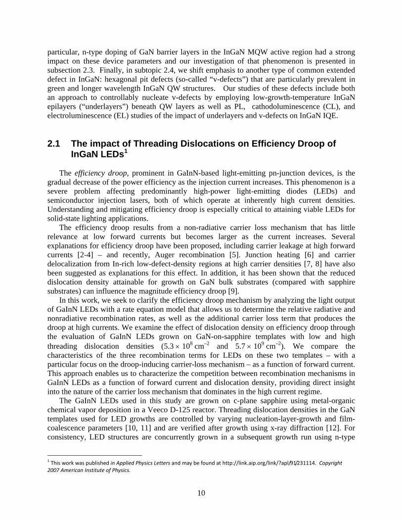
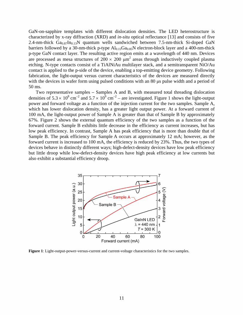
Two representative samples – Samples A and B, with measured total threading dislocation densities of 5.3 108 cm–2 and 5.7 109 cm–2 – are investigated. Figure 1 shows the light-output power and forward voltage as a function of the injection current for the two samples. Sample A, which has lower dislocation density, has a greater light output power. At a forward current of 100 mA, the light-output power of Sample A is greater than that of Sample B by approximately 67%. Figure 2 shows the external quantum efficiency of the two samples as a function of the forward current. Sample B exhibits little decrease in the efficiency as current increases, but has low peak efficiency. In contrast, Sample A has peak efficiency that is more than double that of Sample B. The peak efficiency for Sample A occurs at approximately 12 mA; however, as the forward current is increased to 100 mA, the efficiency is reduced by 23%. Thus, the two types of devices behave in distinctly different ways; high-defect-density devices have low peak efficiency but little droop while low-defect-density devices have high peak efficiency at low currents but also exhibit a substantial efficiency droop.
Figure 1: Light-output-power-versus-current and current-voltage characteristics for the two samples.
12
Figure 2: External quantum efficiency as a function of forward current
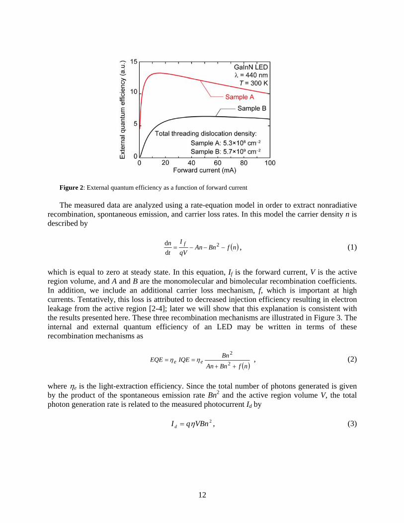
The measured data are analyzed using a rate-equation model in order to extract nonradiative
recombination, spontaneous emission, and carrier loss rates. In this model the carrier density n is described by
nfBnAnqV
I
t
n f 2
d
d , (1)
which is equal to zero at steady state. In this equation, If is the forward current, V is the active region volume, and A and B are the monomolecular and bimolecular recombination coefficients. In addition, we include an additional carrier loss mechanism, f, which is important at high currents. Tentatively, this loss is attributed to decreased injection efficiency resulting in electron leakage from the active region [2-4]; later we will show that this explanation is consistent with the results presented here. These three recombination mechanisms are illustrated in Figure 3. The internal and external quantum efficiency of an LED may be written in terms of these recombination mechanisms as
nfBnAn
BnIQEEQE ee
2
2 , (2)
where e is the light-extraction efficiency. Since the total number of photons generated is given by the product of the spontaneous emission rate Bn2 and the active region volume V, the total photon generation rate is related to the measured photocurrent Id by 2VBnqI d , (3)
13
where the factor depends upon the light-extraction efficiency, the fraction of emitted photons emitted that are collected by the detector, and the quantum efficiency of the detector; is taken to be equal for both samples. For the bimolecular recombination coefficient B, we have assumed a value of 110–10 cm3/s, which is a typical number [14]. When , B, and the active region volume V are known, an estimate of the carrier density at a given forward current can be obtained from Eqn. 3. The calculated recombination rates as a function of current are then used as the basis for our comparison of low and high dislocation density LEDs.
Figure 3: Schematic illustration of the three recombination mechanisms considered in this work
The monomolecular recombination rate can be determined by fitting the light-output-versus-
current curve at low forward current values, where f can be neglected. Using the extracted value for n, the light-output-versus-current curve in Figure 1 is then fitted by choosing the value for A. The form of the monomolecular recombination term – An – is valid under conditions of equal high-level injection of electrons and holes. Because this condition is not exactly met in practice, and to allow for a closer fit to the measured data, the exponent of the carrier density in the monomolecular recombination term is allowed to deviate slightly from 1. For samples A and B this exponent is 1.2 and 0.76, respectively. The nonradiative recombination term can also be written in terms of a carrier-density-dependent lifetime,
n
nR
nrnr (4)
At a density of 1018 cm-3, the nonradiative lifetimes are 12.3 ns and 6.4 ns for samples A and B, respectively.
Using the above estimates of the rate parameters A and B, Figure 4 compares the measured external quantum efficiency to Eqn. 2 with the leakage term set to zero (f = 0) for both samples as a function of forward current. The carrier density is also shown in the figure. When the current remains below 5 mA, a good match is achieved with only the monomolecular recombination and spontaneous emission terms. At approximately 10 mA, the peak efficiency in Sample A is reached and then the droop begins. At this point, the basic rate equation that includes only spontaneous emission and monomolecular recombination – which predicts a non-decreasing efficiency – should be expected to fail. To obtain the additional carrier loss term, f, that causes this failure, we can now simply take the difference between the fitted and measured curves shown in Figure 4.
14
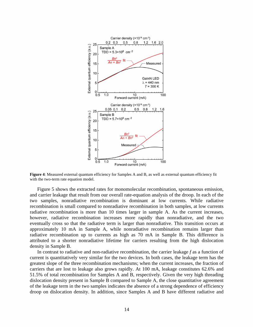
Figure 4: Measured external quantum efficiency for Samples A and B, as well as external quantum efficiency fit with the two-term rate equation model.
Figure 5 shows the extracted rates for monomolecular recombination, spontaneous emission,
and carrier leakage that result from our overall rate-equation analysis of the droop. In each of the two samples, nonradiative recombination is dominant at low currents. While radiative recombination is small compared to nonradiative recombination in both samples, at low currents radiative recombination is more than 10 times larger in sample A. As the current increases, however, radiative recombination increases more rapidly than nonradiative, and the two eventually cross so that the radiative term is larger than nonradiative. This transition occurs at approximately 10 mA in Sample A, while nonradiative recombination remains larger than radiative recombination up to currents as high as 70 mA in Sample B. This difference is attributed to a shorter nonradiative lifetime for carriers resulting from the high dislocation density in Sample B.
In contrast to radiative and non-radiative recombination, the carrier leakage f as a function of current is quantitatively very similar for the two devices. In both cases, the leakage term has the greatest slope of the three recombination mechanisms; when the current increases, the fraction of carriers that are lost to leakage also grows rapidly. At 100 mA, leakage constitutes 62.6% and 51.5% of total recombination for Samples A and B, respectively. Given the very high threading dislocation density present in Sample B compared to Sample A, the close quantitative agreement of the leakage term in the two samples indicates the absence of a strong dependence of efficiency droop on dislocation density. In addition, since Samples A and B have different radiative and
15
nonradiative rates and carrier densities at a given injection current, the leakage term is not a direct function of carrier density and is not dependent on the radiative and nonradiative recombination mechanisms in the active region. Instead, the leakage term f depends primarily on the forward current. These characteristics are consistent with the carrier leakage explanation for the efficiency droop.
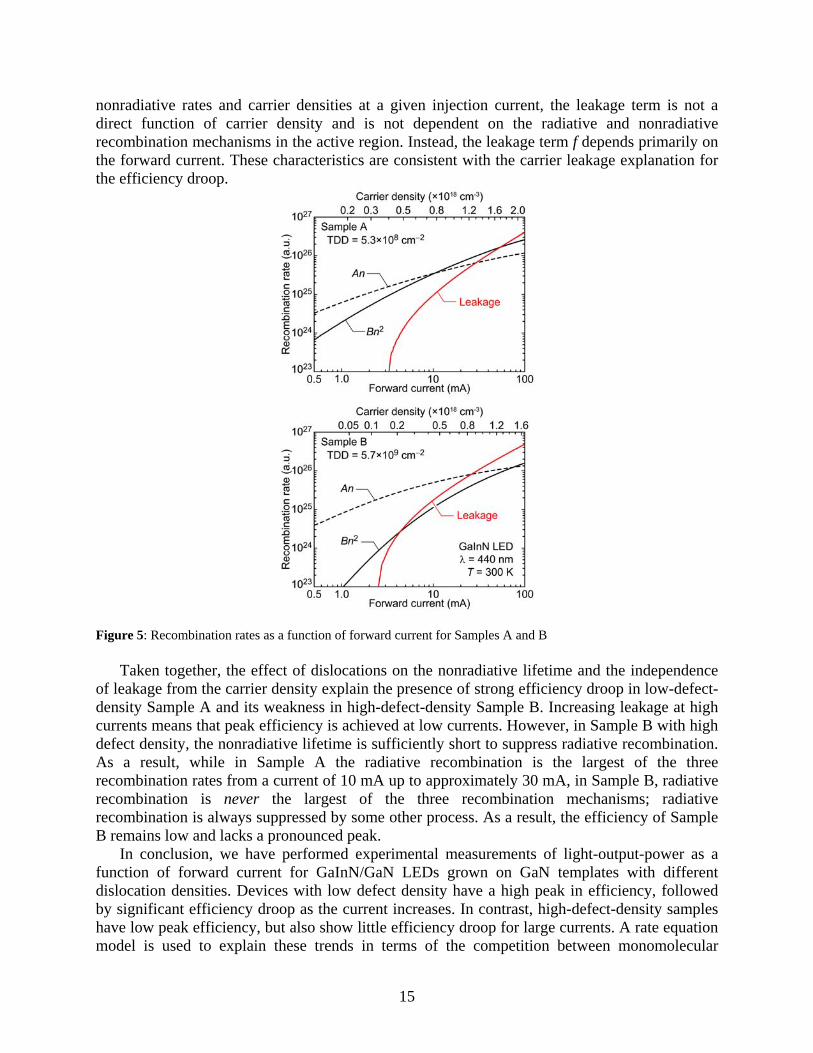
Figure 5: Recombination rates as a function of forward current for Samples A and B
Taken together, the effect of dislocations on the nonradiative lifetime and the independence of leakage from the carrier density explain the presence of strong efficiency droop in low-defect-density Sample A and its weakness in high-defect-density Sample B. Increasing leakage at high currents means that peak efficiency is achieved at low currents. However, in Sample B with high defect density, the nonradiative lifetime is sufficiently short to suppress radiative recombination. As a result, while in Sample A the radiative recombination is the largest of the three recombination rates from a current of 10 mA up to approximately 30 mA, in Sample B, radiative recombination is never the largest of the three recombination mechanisms; radiative recombination is always suppressed by some other process. As a result, the efficiency of Sample B remains low and lacks a pronounced peak.
In conclusion, we have performed experimental measurements of light-output-power as a function of forward current for GaInN/GaN LEDs grown on GaN templates with different dislocation densities. Devices with low defect density have a high peak in efficiency, followed by significant efficiency droop as the current increases. In contrast, high-defect-density samples have low peak efficiency, but also show little efficiency droop for large currents. A rate equation model is used to explain these trends in terms of the competition between monomolecular
16
nonradiative recombination, radiative recombination, and an additional recombination term that dominates at high currents. Our analysis reveals that this high-current recombination term is quantitatively very similar for LEDs of different dislocation densities, thereby indicating that dislocations are not driving the efficiency droop at high currents. Instead, the primary effect of dislocations is in the low current regime where high defect densities correlate with increased dominance of nonradiative recombination and a pronounced suppression of the peak efficiency. The high-current recombination term is independent of dislocation density, as well as the monomolecular nonradiative and radiative recombination rates. This independence, along with the strikingly similar forward-current dependence for each sample, is consistent with a carrier leakage mechanism at high currents. 2.2. Impact of Threading Dislocations on InGaN Quantum Well
Internal Quantum Efficiency and Non-Radiative Coefficient*
GaInN/GaN multiple-quantum-well (MQW) light-emitting diodes (LEDs) are highly efficient semiconductor sources of short-wavelength visible light. However, the direct and accurate measurement of the MQW internal quantum efficiency (IQE) as a function of carrier concentration remains to be a continuing challenge. Previously, the IQE of III-V semiconductor quantum wells has been determined by absolute intensity measurements using an integrating sphere [15], a steady-state thermal study [16], time-resolved photoluminescence (PL) [17], temperature-dependent relative IQE measurements [18,19], and methods based on a semiconductor rate equation analysis [20-22]. In the present work, we determine the IQE of GaInN/GaN MQWs from the dependence of integrated PL intensity on excitation power [20]. We apply this technique to a series of MQW samples with different threading-dislocation densities and establish both the IQE versus carrier concentration and the non-radiative coefficient, A. Our PL measurements employ selective optical pumping of the GaInN QW layers to avoid carrier-generation in the barrier layers and reduce carrier transport effects. This delineation is of interest to more clearly isolate recombination processes in GaInN MQWs, given the potential for carrier injection and carrier leakage to contribute to the “efficiency droop” in electroluminescence (EL)-based measurements of GaInN-based LEDs at high carrier densities [23-25].
The GaInN/GaN MQW LED heterostructures are grown on GaN-on-sapphire templates by metal-organic vapor-phase epitaxy. The threading-dislocation densities of the templates are controlled by varying nucleation-layer-growth and film-coalescence parameters [24,26,27]. Threading-dislocation densities are evaluated using x-ray diffraction (XRD) rocking-curve measurements of the Bragg peakwidths of the (0004) and (10-11) reflections of GaN. Threading-dislocation densities are extracted from the measured peakwidths using equations described in Ref. 28. For the edge-type threading dislocations predominating in typical GaN-on-sapphire templates, previous work finds that these XRD measurements of threading-dislocation density agree with transmission electron microscopy to within a standard error of ~33% [28]. To avoid extrinsic sources of IQE variation, the LED epi-structures are grown in the same growth run on three different templates. The MQW structure has five 2.4-nm-thick Ga0.87In0.13N QWs
* This work was published in Applied Physics Letters and may be found at http://link.aip.org/link/?apl/94/111109. Copyright
2009 American Institute of Physics.
17
sandwiched between 7.5-nm-thick Si-doped GaN quantum barriers, followed by a 30-nm-thick p-type Al0.15Ga0.85N electron-block layer and a 400-nm-thick p-type GaN contact layer [24]. For the three resulting LED wafers in this study, named A, B, and C, we have measured total threading-dislocation densities of 5.7×109 cm2, 1.2×109 cm2, and 5.3×108 cm2, respectively.
Our PL studies employ a 405-nm laser diode as an excitation source to enable photoexcited carrier generation only in the GaInN QWs. By applying this exclusive quantum well excitation, we avoid optical carrier generation in the barrier layers and reduce carrier transport effects occurring in EL measurements. The laser diode is operated in a pulsed mode, with a 100 s period and 1% duty cycle. To vary the carrier concentration, the laser diode injection current is increased from 50 mA to 180 mA, with a 10 mA interval, producing incident peak power densities ranging from 0.21 kWcm2 to 1.88 kWcm2.
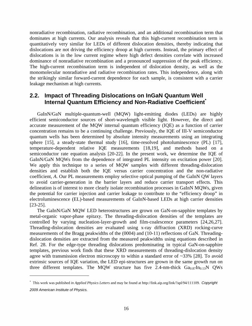
The resulting MQW emission spectra are modulated by a periodic interference term, as shown by three representative spectra that result from each of our three samples in Figure 6(a). The interference is caused by the formation of an optical resonator formed by the GaN/sapphire and GaN/air interfaces. Our measurements show that the spectra of GaInN/GaN MQWs grown on GaN substrates [23] have no such interference, and can be fitted very well by a Lorentzian distribution, as shown by Figure 6(b). Given this clear underlying dependence, we obtain integrated PL intensities by fitting our modulated spectra to a Lorentzian distribution. Figure 6(a) also shows the corresponding Lorentzian fits for the three spectra. To avoid the laser-emission tail during spectral fitting and integration, a limited PL-wavelength range from 425 nm to 500 nm is used.
Figure 6: (a) Representative spectra and the corresponding Lorentzian fits for three samples with varying dislocation densities, and (b) (insert) a representative spectrum and a Lorentzian fit for a GaInN/GaN MQW LED heterostructure grown on a bulk-GaN substrate.
Next, we present a theoretical model: The three main carrier-recombination mechanisms in a
bulk semiconductor are Shockley-Read-Hall (SRH) non-radiative recombination, expressed as An, bimolecular radiative recombination, Bn2, and Auger non-radiative recombination, Cn3, where A, B and C are the respective recombination coefficients and n is the carrier concentration. Auger recombination affects LED efficiency only at very high excitation; thus, in our experiments, the generation rate and the IQE at steady state can be expressed as:
18
2total BnAnRG (1)
GBnBnAnBnIQE 222 )( , (2) and the integrated PL intensity can be expressed as
2PL BnI , (3)
where is a constant determined by the volume of the excited active region and the total collection efficiency of luminescence. By eliminating n in Eq. 1 and Eq. 3, we can express the generation rate in terms of integrated PL intensity:
PLPL
1II
B
AG
. (4)
The connection between theory and experiment is completed by noting that the generation
rate can be separately calculated from experimental parameters using
)()1()()1( spotlaserspotlaser hARPlhAlRPG , (5)
where Plaser is the peak optical power incident on the sample, R (18%) is the Fresnel reflection at the sample surface, l (12 nm) is the total thickness of the GaInN QWs, Aspot (3.5×103 µm) is the area of the laser spot on the sample surface, h (3.07 eV) is the energy of a 405-nm photon, and α (5.4 µm1) is the absorption coefficient of the Ga0.87In0.13N well at 405 nm. The absorption coefficient is calculated from its square-root dependence on energy [29]:
gg EEE /)(0 , (6)
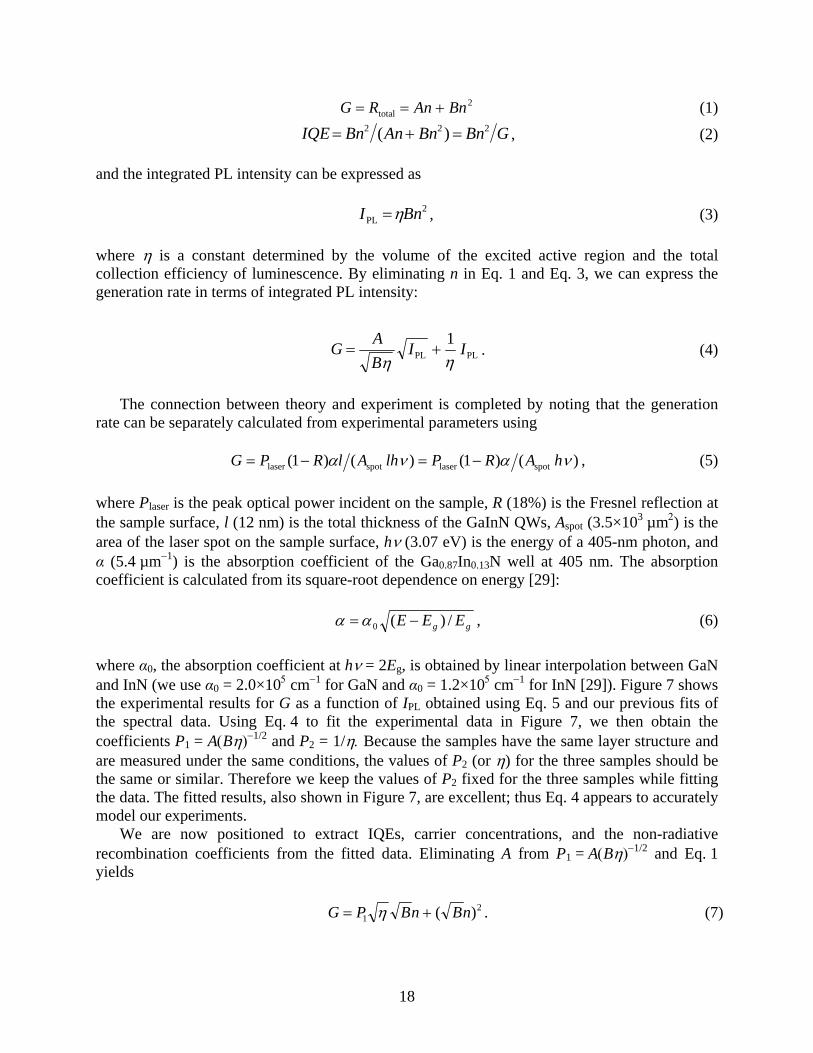
where α0, the absorption coefficient at h = 2Eg, is obtained by linear interpolation between GaN and InN (we use α0 = 2.0×10cm1 for GaN and α0 = 1.2×10cm1 for InN [29]). Figure 7 shows the experimental results for G as a function of IPL obtained using Eq. 5 and our previous fits of the spectral data. Using Eq. 4 to fit the experimental data in Figure 7, we then obtain the coefficients P1 = AB1/2 and P2 = 1/ Because the samples have the same layer structure and are measured under the same conditions, the values of P2 (or ) for the three samples should be the same or similar. Therefore we keep the values of P2 fixed for the three samples while fitting the data. The fitted results, also shown in Figure 7, are excellent; thus Eq. 4 appears to accurately model our experiments.
We are now positioned to extract IQEs, carrier concentrations, and the non-radiative recombination coefficients from the fitted data. Eliminating A from P1 = AB1/2 and Eq. 1 yields
21 )( nBnBPG . (7)
19
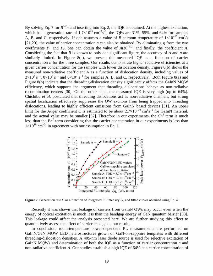
By solving Eq. 7 for B1/2n and inserting into Eq. 2, the IQE is obtained. At the highest excitation, which has a generation rate of 1.7×1026 cm3s1, the IQEs are 31%, 55%, and 64% for samples A, B, and C, respectively. If one assumes a value of B at room temperature of 1×1010 cm3/s [21,29], the value of carrier concentration n can also be obtained. By eliminating from the two coefficients P1 and P2, one can obtain the value of A(B)1/2, and finally, the coefficient A. Considering the fact that B is known to only one significant figure, the accuracy of A and n are similarly limited. In Figure 8(a), we present the measured IQE as a function of carrier concentration n for the three samples. Our results demonstrate higher radiative efficiencies at a given carrier concentration for the samples with lower dislocation density. Figure 8(b) shows the measured non-radiative coefficient A as a function of dislocation density, including values of 2×10⁸ s1, 8×10⁷ s1 and 6×10⁷ s1 for samples A, B, and C, respectively. Both Figure 8(a) and Figure 8(b) indicate that the threading-dislocation density significantly affects the GaInN MQW efficiency, which supports the argument that threading dislocations behave as non-radiative recombination centers [30]. On the other hand, the measured IQE is very high (up to 64%). Chichibu et al. postulated that threading dislocations act as non-radiative channels, but strong spatial localization effectively suppresses the QW excitons from being trapped into threading dislocations, leading to highly efficient emissions from GaInN based devices [31]. An upper limit for the Auger coefficient C is estimated to be about 2.7×1030 cm6s1 for GaInN material, and the actual value may be smaller [32]. Therefore in our experiments, the Cn3 term is much less than the Bn2 term considering that the carrier concentration in our experiments is less than 1×1018 cm3, in agreement with our assumption in Eq. 1.
Figure 7: Generation rate G as a function of integrated PL intensity IPL and fitted curves obtained using Eq. 4.
Recently it was shown that leakage of carriers from GaInN QWs may occur even when the energy of optical excitation is much less than the bandgap energy of GaN quantum barrier [33]. This leakage could affect the analysis presented here. We are further studying this effect to quantitatively assess the effect of carrier leakage on our results.
In conclusion, room-temperature power-dependent PL measurements are performed on GaInN/GaN MQW LED heterostructures grown on GaN-on-sapphire templates with different threading-dislocation densities. A 405-nm laser diode source is used for selective excitation of GaInN MQWs and determination of both the IQE as a function of carrier concentration n and non-radiative coefficient A. Our studies establish a high IQE of 64% at a carrier concentration of
20
1×1018 cm3 for the sample with the lowest dislocation density (5.3×108 cm2). The measured non-radiative recombination coefficient, A, varies from 6×10⁷ s1 to 2×10⁸ s1 as the dislocation density increases from 5.3×108 cm2 to 5.7×109 cm2, respectively, confirming the non-radiative nature of these defects.
Figure 8: (a) Internal quantum efficiency as a function of carrier concentration and (b) non-radiative coefficient A as a function of threading-dislocation density.
2.3. The Origin of High ideality Factors in InGaN LEDs*
In recent years, great progress has been made in developing high-efficiency, high-power GaN-based ultraviolet [34] and blue [35] light-emitting diodes (LEDs). In order to further improve the device performance, a number of material- and device-related problems must be resolved. As one of the commonly-used parameters, the diode-ideality factor is directly related to carrier transport, recombination, and resistivity. A high diode-ideality factor results in a high forward voltage, and thus limits the power efficiency. However, it is well known that III-N-based p-n junctions with multiple quantum wells (MQWs) can have abnormally high diode-ideality factors ( 75ideality n ) [36-41]. This phenomenon has been a scientific “puzzle” for more than a
decade, and the physical origin has not yet been fully identified.
* This work was published in Applied Physics Letters and may be found at http://link.aip.org/link/?apl/94/081113. Copyright
2009 American Institute of Physics.
21
Ideality factors between 1.0 to 2.0 are normally attributed to the competition between the carrier drift-diffusion process and the Sah-Noyce-Shockley generation-recombination process [42]. Ideality factors exceeding 2.0 have been suggested to originate from additional current paths including the trap-assisted tunneling [37-40] and carrier leakage [40]. However, no quantitative attempts have been reported to connect these two mechanisms to the abnormally high ideality factors found experimentally in GaN-based LEDs.
Shah et al. [36] proposed that GaN-based LEDs can be modeled as a series of rectifying unipolar heterojunctions and metal semiconductor junctions, each having an associated ideality factor. The Shockley diode equation for qkTV /3 can then be rewritten as the summation of voltages dropping across individual rectifying junctions denoted by the subscript i [36],
(1) lnln S, ideality, ideality,
iii
ii
ii In
q
kTIn
q
kTVV
where SI is the reverse saturation current, q is the elementary charge, k is the Boltzmann
constant, T is the absolute temperature, and idealityn is the ideality factor. This dependence reveals
that the ideality factors of individual rectifying junctions add up to the total device ideality factor as i inn ideality,ideality which can lead to a high ideality factor of 5 to 7 when the p-n junction of
the diode, a non-ohmic metal-semiconductor junction and other rectifying junctions are considered. Shah et al. measured the ideality factor of a GaN-based p-n diode and a GaN-based p-n diode having a p-type AlGaN/GaN superlattice on top of the p-n junction, and showed that the ideality factor decreases with improved ohmic behavior of metal-to-p-type-semiconductor contact. In this letter, we expand these considerations to the MQW active region of the LED and investigate the impact of unipolar heterojunctions formed in the MQW active region on the ideality factor. We report experimental results on the ideality factor of GaInN/GaN blue LEDs emitting at nm 450 with a controlled number of doped QBs, and show that the high ideality factor is primarily caused by the GaN heterojunction QBs in the MQW active region.
Four GaInN/GaN MQW LEDs, each comprising 5 Ga0.85In0.15N QWs, were grown on sapphire substrates using metal-organic vapor-phase epitaxy. (0002) x-ray diffraction scans and dynamic diffraction fits were performed to obtain the QW and QB thicknesses and the QW In composition. The MQW consists of 2.5-nm-thick GaInN QWs and 8.2-nm-thick GaN QBs followed by a 2030-nm-thick GaN spacer layer, an AlGaN electron-blocking layer (EBL), and a p-type GaN cladding layer. The four LED heterostructures are distinguished by the number of QBs that are intentionally Si-doped, and we employ doping in 1, 2, 3, and 4 of the QBs, as depicted in the inset of Figure 9(a). A barrier-doping level of 318 cm 103 n is determined by Hall-effect measurements of thick reference GaN layers grown under the same conditions as the doped QBs. The four LED heterostructures are fabricated into 2μm 300300 LED devices and characterized in terms of their electrical characteristics.
The I-V characteristics of the LEDs are measured using a semiconductor parameter analyzer. A dependence of voltage V on injection current I from 0.01 mA to 10 mA is measured and displayed using a logarithmic current scale for the four LED structures as shown on the left-hand side of Figure 9. The corresponding ideality factors are shown on the right-hand side of Figure 9 and are inferred from the measurement using
22
(2) )ln( 1
idealityV
IkT
qn
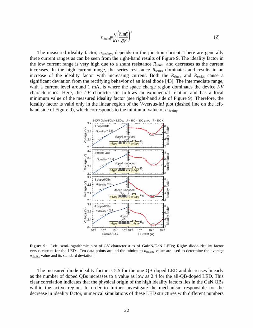
The measured ideality factor, nideality, depends on the junction current. There are generally
three current ranges as can be seen from the right-hand results of Figure 9. The ideality factor in the low current range is very high due to a shunt resistance Rshunt, and decreases as the current increases. In the high current range, the series resistance Rseries dominates and results in an increase of the ideality factor with increasing current. Both the Rshunt and Rseries cause a significant deviation from the rectifying behavior of an ideal diode [43]. The intermediate range, with a current level around 1 mA, is where the space charge region dominates the device I-V characteristics. Here, the I-V characteristic follows an exponential relation and has a local minimum value of the measured ideality factor (see right-hand side of Figure 9). Therefore, the ideality factor is valid only in the linear region of the V-versus-lnI plot (dashed line on the left-hand side of Figure 9), which corresponds to the minimum value of nideality.
Figure 9: Left: semi-logarithmic plot of I-V characteristics of GaInN/GaN LEDs; Right: diode-ideality factor versus current for the LEDs. Ten data points around the minimum nideality value are used to determine the average nideality value and its standard deviation.
The measured diode ideality factor is 5.5 for the one-QB-doped LED and decreases linearly as the number of doped QBs increases to a value as low as 2.4 for the all-QB-doped LED. This clear correlation indicates that the physical origin of the high ideality factors lies in the GaN QBs within the active region. In order to further investigate the mechanism responsible for the decrease in ideality factor, numerical simulations of these LED structures with different numbers
23
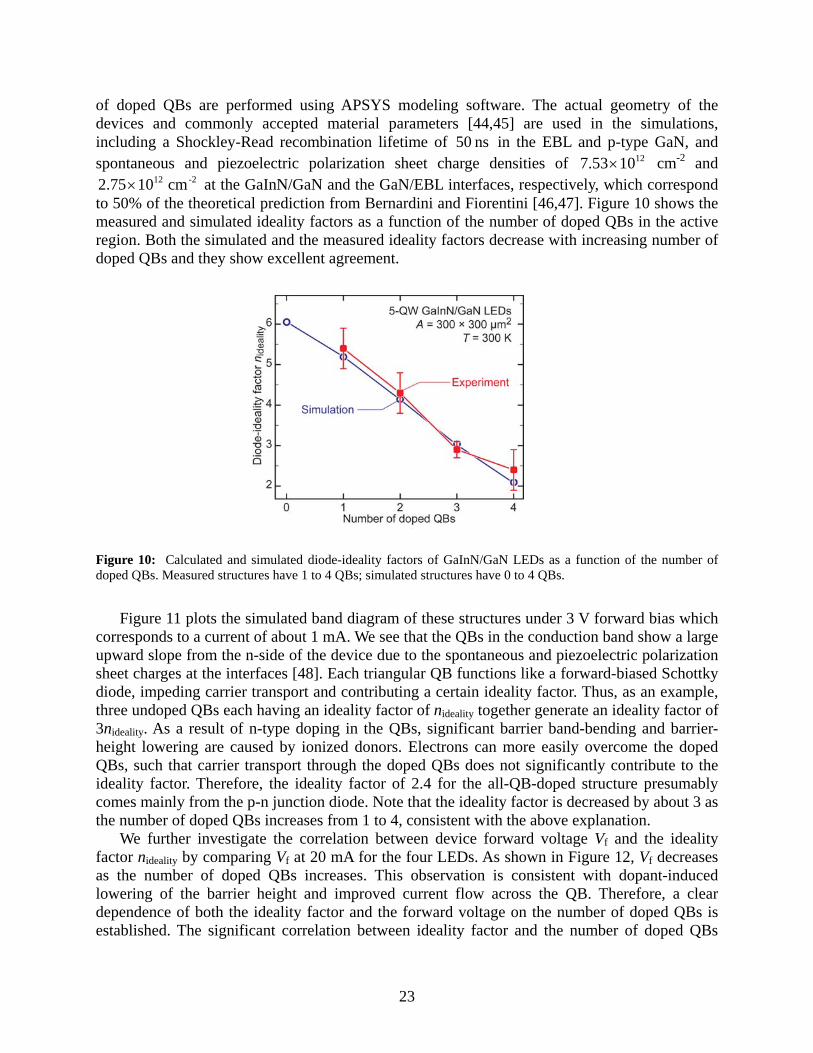
of doped QBs are performed using APSYS modeling software. The actual geometry of the devices and commonly accepted material parameters [44,45] are used in the simulations, including a Shockley-Read recombination lifetime of ns 50 in the EBL and p-type GaN, and spontaneous and piezoelectric polarization sheet charge densities of 121053.7 cm-2 and
-212 cm 10.752 at the GaInN/GaN and the GaN/EBL interfaces, respectively, which correspond to 50% of the theoretical prediction from Bernardini and Fiorentini [46,47]. Figure 10 shows the measured and simulated ideality factors as a function of the number of doped QBs in the active region. Both the simulated and the measured ideality factors decrease with increasing number of doped QBs and they show excellent agreement.
Figure 10: Calculated and simulated diode-ideality factors of GaInN/GaN LEDs as a function of the number of doped QBs. Measured structures have 1 to 4 QBs; simulated structures have 0 to 4 QBs.
Figure 11 plots the simulated band diagram of these structures under 3 V forward bias which
corresponds to a current of about 1 mA. We see that the QBs in the conduction band show a large upward slope from the n-side of the device due to the spontaneous and piezoelectric polarization sheet charges at the interfaces [48]. Each triangular QB functions like a forward-biased Schottky diode, impeding carrier transport and contributing a certain ideality factor. Thus, as an example, three undoped QBs each having an ideality factor of nideality together generate an ideality factor of 3nideality. As a result of n-type doping in the QBs, significant barrier band-bending and barrier-height lowering are caused by ionized donors. Electrons can more easily overcome the doped QBs, such that carrier transport through the doped QBs does not significantly contribute to the ideality factor. Therefore, the ideality factor of 2.4 for the all-QB-doped structure presumably comes mainly from the p-n junction diode. Note that the ideality factor is decreased by about 3 as the number of doped QBs increases from 1 to 4, consistent with the above explanation.
We further investigate the correlation between device forward voltage Vf and the ideality factor nideality by comparing Vf at 20 mA for the four LEDs. As shown in Figure 12, Vf decreases as the number of doped QBs increases. This observation is consistent with dopant-induced lowering of the barrier height and improved current flow across the QB. Therefore, a clear dependence of both the ideality factor and the forward voltage on the number of doped QBs is established. The significant correlation between ideality factor and the number of doped QBs
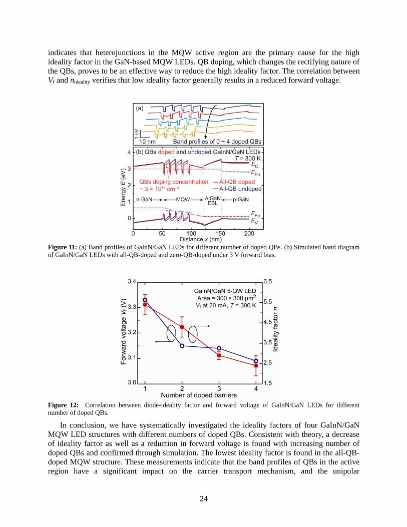
24
indicates that heterojunctions in the MQW active region are the primary cause for the high ideality factor in the GaN-based MQW LEDs. QB doping, which changes the rectifying nature of the QBs, proves to be an effective way to reduce the high ideality factor. The correlation between Vf and nideality verifies that low ideality factor generally results in a reduced forward voltage.
Figure 11: (a) Band profiles of GaInN/GaN LEDs for different number of doped QBs. (b) Simulated band diagram of GaInN/GaN LEDs with all-QB-doped and zero-QB-doped under 3 V forward bias.
Figure 12: Correlation between diode-ideality factor and forward voltage of GaInN/GaN LEDs for different number of doped QBs.
In conclusion, we have systematically investigated the ideality factors of four GaInN/GaN MQW LED structures with different numbers of doped QBs. Consistent with theory, a decrease of ideality factor as well as a reduction in forward voltage is found with increasing number of doped QBs and confirmed through simulation. The lowest ideality factor is found in the all-QB-doped MQW structure. These measurements indicate that the band profiles of QBs in the active region have a significant impact on the carrier transport mechanism, and the unipolar
25
heterojunctions inside the active region play a role in determining the ideality factor.
2.4. The impact of V-defects and InGaN “underlayers” on the quantum efficiency of InGaN MQWs and LEDs
Another common extended defect in InGaN materials is the so-called “v-defect”. This
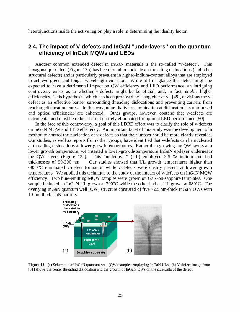
hexagonal pit defect (Figure 13b) has been found to nucleate on threading dislocations (and other structural defects) and is particularly prevalent in higher-indium-content alloys that are employed to achieve green and longer wavelength emission. While at first glance this defect might be expected to have a detrimental impact on QW efficiency and LED performance, an intriguing controversy exists as to whether v-defects might be beneficial, and, in fact, enable higher efficiencies. This hypothesis, which has been proposed by Hangleiter et al. [49], envisions the v-defect as an effective barrier surrounding threading dislocations and preventing carriers from reaching dislocation cores. In this way, nonradiative recombination at dislocations is minimized and optical efficiencies are enhanced. Other groups, however, contend that v-defects are detrimental and must be reduced if not entirely eliminated for optimal LED performance [50].
In the face of this controversy, a goal of this LDRD effort was to clarify the role of v-defects on InGaN MQW and LED efficiency. An important facet of this study was the development of a method to control the nucleation of v-defects so that their impact could be more clearly revealed. Our studies, as well as reports from other groups, have identified that v-defects can be nucleated at threading dislocations at lower growth temperatures. Rather than growing the QW layers at a lower growth temperature, we inserted a lower-growth-temperature InGaN epilayer underneath the QW layers (Figure 13a). This “underlayer” (UL) employed 2-9 % indium and had thicknesses of 50-300 nm. Our studies showed that UL growth temperatures higher than ~850°C eliminated v-defect formation while v-defects were clearly present at lower growth temperatures. We applied this technique to the study of the impact of v-defects on InGaN MQW efficiency. Two blue-emitting MQW samples were grown on GaN-on-sapphire templates. One sample included an InGaN UL grown at 790°C while the other had an UL grown at 880°C. The overlying InGaN quantum well (QW) structure consisted of five ~2.5 nm-thick InGaN QWs with 10-nm thick GaN barriers.
Figure 13: (a) Schematic of InGaN quantum well (QW) samples employing InGaN ULs. (b) V-defect image from [51] shows the center threading dislocation and the growth of InGaN QWs on the sidewalls of the defect.
Sapphire substrate
LT InGaNunderlayer
High tempGaN
Threading dislocations decorated by “ V -defects ”
InGaN QWs
Sapphire substrate
LT InGaNunderlayer
High tempGaN
Threading dislocations decorated by “ V -defects ”
InGaN QWs
(b) (a)
26
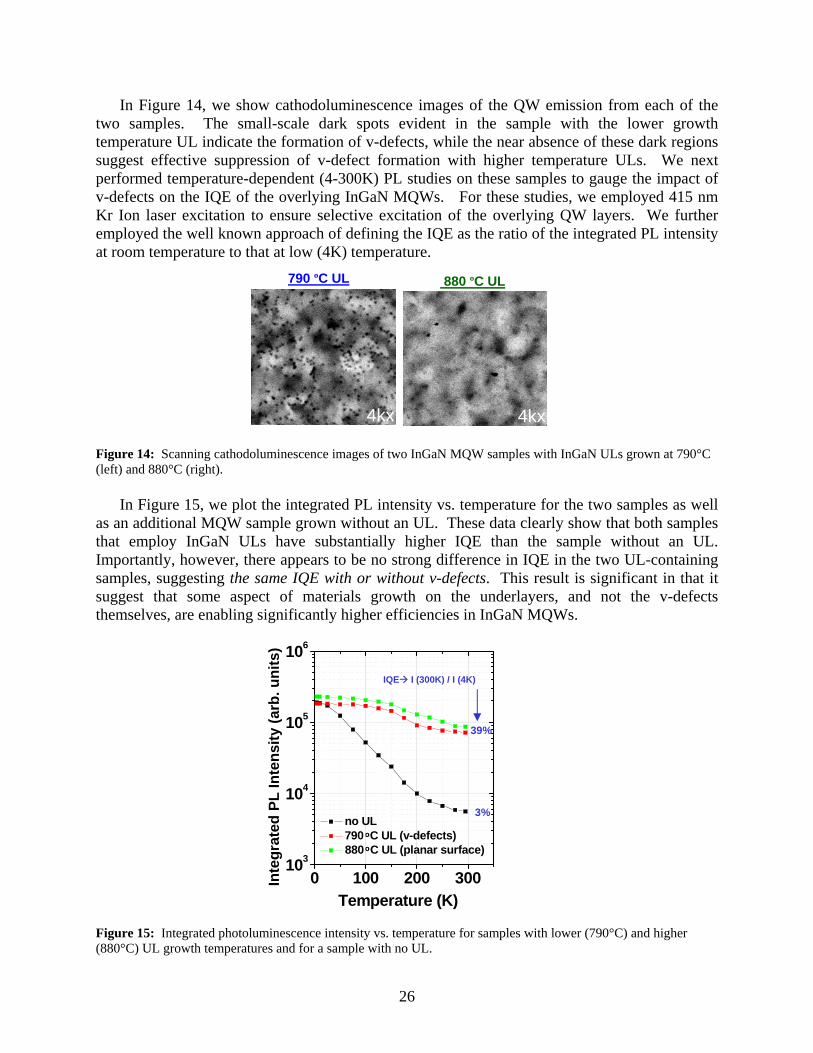
In Figure 14, we show cathodoluminescence images of the QW emission from each of the two samples. The small-scale dark spots evident in the sample with the lower growth temperature UL indicate the formation of v-defects, while the near absence of these dark regions suggest effective suppression of v-defect formation with higher temperature ULs. We next performed temperature-dependent (4-300K) PL studies on these samples to gauge the impact of v-defects on the IQE of the overlying InGaN MQWs. For these studies, we employed 415 nm Kr Ion laser excitation to ensure selective excitation of the overlying QW layers. We further employed the well known approach of defining the IQE as the ratio of the integrated PL intensity at room temperature to that at low (4K) temperature.
Figure 14: Scanning cathodoluminescence images of two InGaN MQW samples with InGaN ULs grown at 790°C (left) and 880°C (right).
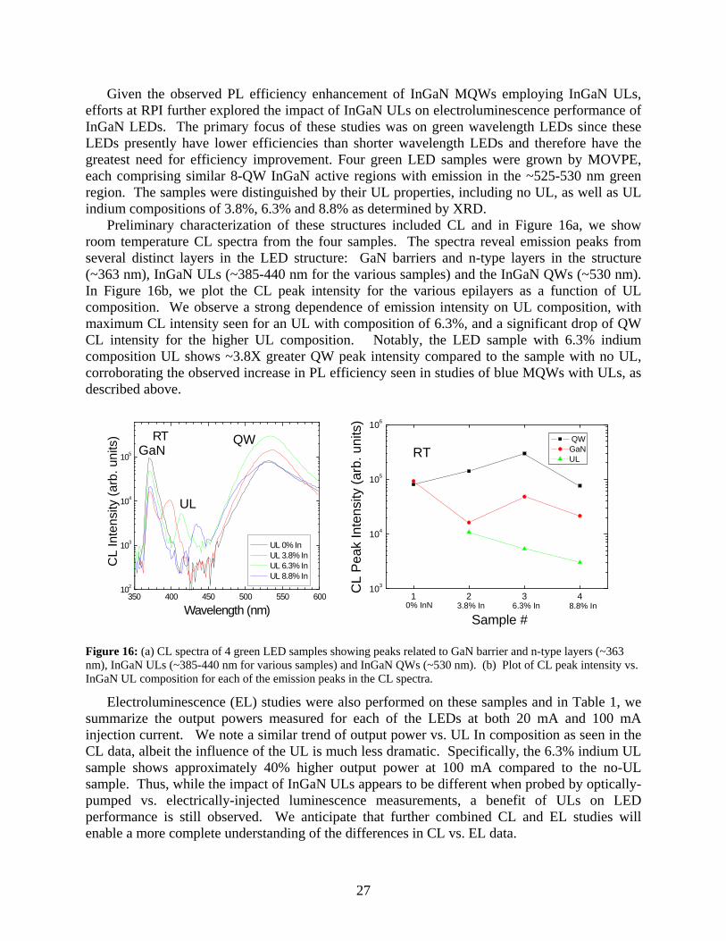
In Figure 15, we plot the integrated PL intensity vs. temperature for the two samples as well
as an additional MQW sample grown without an UL. These data clearly show that both samples that employ InGaN ULs have substantially higher IQE than the sample without an UL. Importantly, however, there appears to be no strong difference in IQE in the two UL-containing samples, suggesting the same IQE with or without v-defects. This result is significant in that it suggest that some aspect of materials growth on the underlayers, and not the v-defects themselves, are enabling significantly higher efficiencies in InGaN MQWs.
Figure 15: Integrated photoluminescence intensity vs. temperature for samples with lower (790°C) and higher (880°C) UL growth temperatures and for a sample with no UL.
4kx4kx
790 ºC UL 880 ºC UL
IQE I (300K) / I (4K)
39%
3%
º º
0 100 200 300103
104
105
106
Inte
gra
ted
PL
Inte
nsi
ty (
arb
. un
its)
Temperature (K)
no UL 790 C UL (v-defects) 880 C UL (planar surface)
27
Given the observed PL efficiency enhancement of InGaN MQWs employing InGaN ULs, efforts at RPI further explored the impact of InGaN ULs on electroluminescence performance of InGaN LEDs. The primary focus of these studies was on green wavelength LEDs since these LEDs presently have lower efficiencies than shorter wavelength LEDs and therefore have the greatest need for efficiency improvement. Four green LED samples were grown by MOVPE, each comprising similar 8-QW InGaN active regions with emission in the ~525-530 nm green region. The samples were distinguished by their UL properties, including no UL, as well as UL indium compositions of 3.8%, 6.3% and 8.8% as determined by XRD.
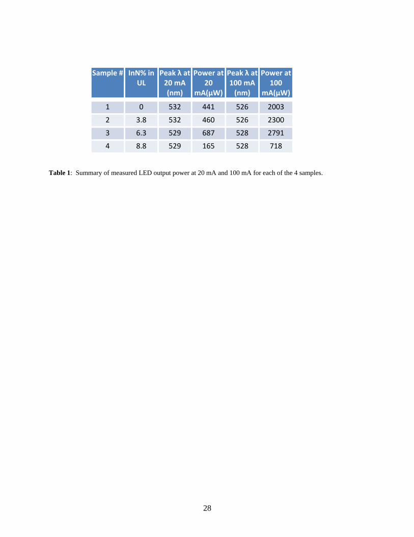
Preliminary characterization of these structures included CL and in Figure 16a, we show room temperature CL spectra from the four samples. The spectra reveal emission peaks from several distinct layers in the LED structure: GaN barriers and n-type layers in the structure (~363 nm), InGaN ULs (~385-440 nm for the various samples) and the InGaN QWs (~530 nm). In Figure 16b, we plot the CL peak intensity for the various epilayers as a function of UL composition. We observe a strong dependence of emission intensity on UL composition, with maximum CL intensity seen for an UL with composition of 6.3%, and a significant drop of QW CL intensity for the higher UL composition. Notably, the LED sample with 6.3% indium composition UL shows ~3.8X greater QW peak intensity compared to the sample with no UL, corroborating the observed increase in PL efficiency seen in studies of blue MQWs with ULs, as described above.
Figure 16: (a) CL spectra of 4 green LED samples showing peaks related to GaN barrier and n-type layers (~363 nm), InGaN ULs (~385-440 nm for various samples) and InGaN QWs (~530 nm). (b) Plot of CL peak intensity vs. InGaN UL composition for each of the emission peaks in the CL spectra.
Electroluminescence (EL) studies were also performed on these samples and in Table 1, we summarize the output powers measured for each of the LEDs at both 20 mA and 100 mA injection current. We note a similar trend of output power vs. UL In composition as seen in the CL data, albeit the influence of the UL is much less dramatic. Specifically, the 6.3% indium UL sample shows approximately 40% higher output power at 100 mA compared to the no-UL sample. Thus, while the impact of InGaN ULs appears to be different when probed by optically-pumped vs. electrically-injected luminescence measurements, a benefit of ULs on LED performance is still observed. We anticipate that further combined CL and EL studies will enable a more complete understanding of the differences in CL vs. EL data.
1 2 3 4103
104
105
106
8.8% In6.3% In0% InN 3.8% In
RT
CL
Pe
ak
Inte
nsi
ty (
arb
. un
its)
Sample #
QWGaNUL
350 400 450 500 550 600102
103
104
105
RT
CL
Inte
nsi
ty (
arb
. uni
ts)
Wavelength (nm)
UL 0% In UL 3.8% In UL 6.3% In UL 8.8% In
QW
UL
GaN
28
Table 1: Summary of measured LED output power at 20 mA and 100 mA for each of the 4 samples.
Sample # InN% in UL
Peak λ at 20 mA (nm)
Power at 20
mA(μW)
Peak λ at 100 mA (nm)
Power at 100
mA(μW)
1 0 532 441 526 2003
2 3.8 532 460 526 2300
3 6.3 529 687 528 2791
4 8.8 529 165 528 718
29
3. Nanoengineering of InGaN LEDs for Enhanced Light Extraction
3.1. Introduction Although LED technology for use in white lighting applications has advanced considerably in the last five years, improvements to light extraction are still required to reach the DOE’s final goal of 90% extraction efficiency. In addition to high extraction efficiencies, it would be desirable to eliminate encapsulants which are currently used in virtually all LED products as these materials have been shown to degrade over time particularly under high power operation. One of the fundamental problems with using LEDs as white light emitters relates to the high index semiconductor which traps the emitted photons inside the semiconductor chip. Both Fresnel reflection inside the escape cone and lateral waveguiding of emitted photons are detrimental to the overall device efficiency. Thus, the high refractive index of the semiconductor materials used for white light LEDs necessitates the use of some form of advanced light extraction for solid-state lighting devices. During the course of this LDRD project, a number of advanced light extraction methods have been investigated, all of which use nanoscale engineering of dielectric or metallic materials. Carefully designed layers of dielectric materials deposited on GaN have been shown to eliminate Fresnel reflection losses. Metallic layers can also be used to increase the efficiency of InGaN LEDs via surface-plasmon-enhanced emission. In both of these cases, nanoscale or microscale lateral patterning is used to extract waveguided modes out of the structure in order to reach the desired efficiency levels. In the following subsections, we overview the progress made on advanced light extraction approaches using both dielectric and metallic materials. 3.2. Nanoengineered dielectric materials for enhanced light
extraction
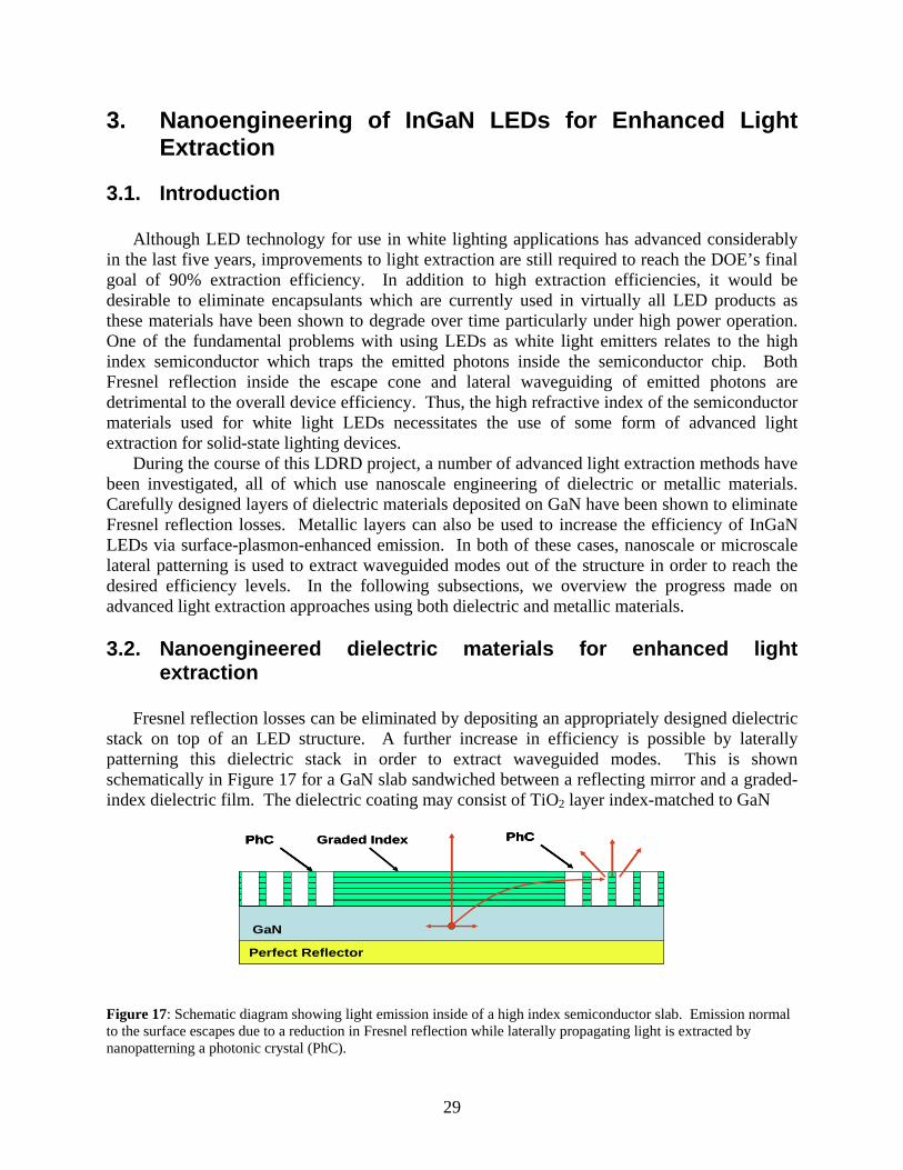
Fresnel reflection losses can be eliminated by depositing an appropriately designed dielectric stack on top of an LED structure. A further increase in efficiency is possible by laterally patterning this dielectric stack in order to extract waveguided modes. This is shown schematically in Figure 17 for a GaN slab sandwiched between a reflecting mirror and a graded-index dielectric film. The dielectric coating may consist of TiO2 layer index-matched to GaN
Figure 17: Schematic diagram showing light emission inside of a high index semiconductor slab. Emission normal to the surface escapes due to a reduction in Fresnel reflection while laterally propagating light is extracted by nanopatterning a photonic crystal (PhC).
Perfect Reflector
GaN
Graded Index PhCPhC
Perfect Reflector
GaN
Graded Index PhCPhCPhCPhC
30
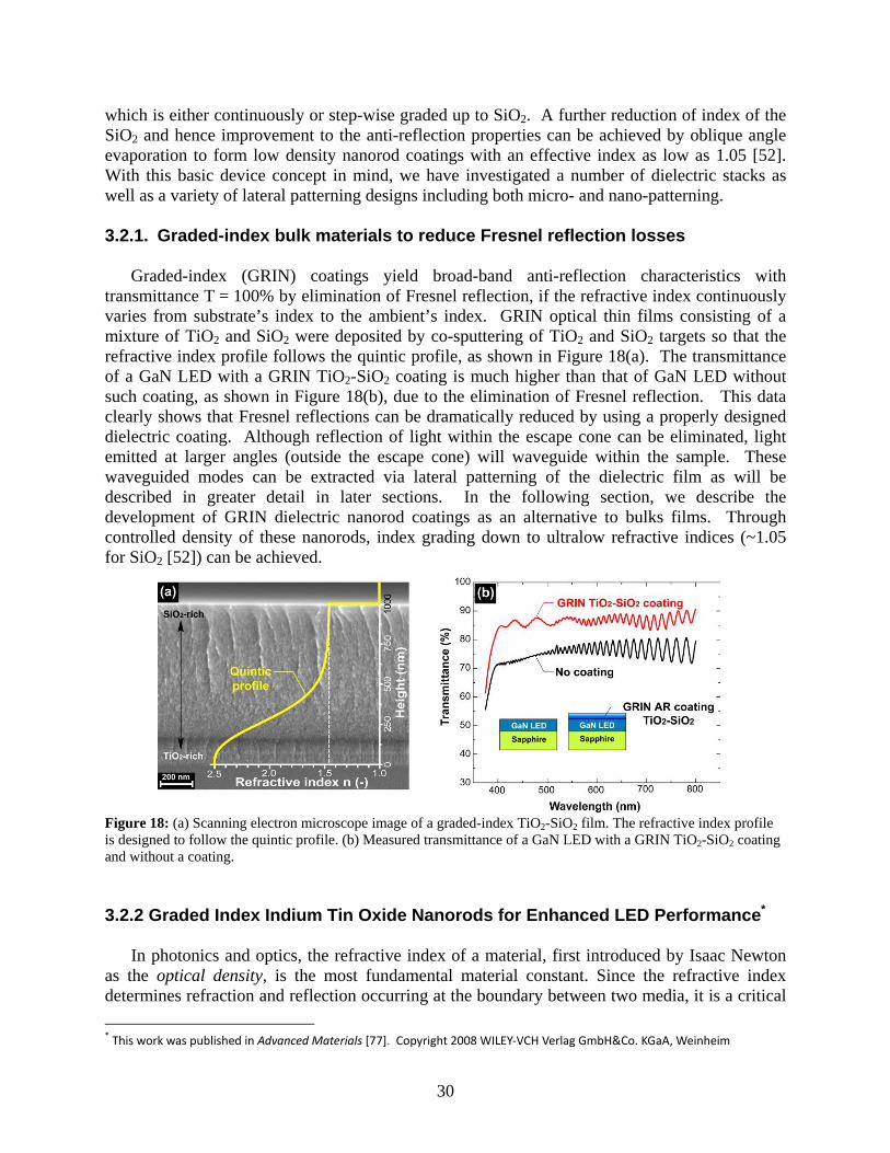
which is either continuously or step-wise graded up to SiO2. A further reduction of index of the SiO2 and hence improvement to the anti-reflection properties can be achieved by oblique angle evaporation to form low density nanorod coatings with an effective index as low as 1.05 [52]. With this basic device concept in mind, we have investigated a number of dielectric stacks as well as a variety of lateral patterning designs including both micro- and nano-patterning. 3.2.1. Graded-index bulk materials to reduce Fresnel reflection losses
Graded-index (GRIN) coatings yield broad-band anti-reflection characteristics with transmittance T = 100% by elimination of Fresnel reflection, if the refractive index continuously varies from substrate’s index to the ambient’s index. GRIN optical thin films consisting of a mixture of TiO2 and SiO2 were deposited by co-sputtering of TiO2 and SiO2 targets so that the refractive index profile follows the quintic profile, as shown in Figure 18(a). The transmittance of a GaN LED with a GRIN TiO2-SiO2 coating is much higher than that of GaN LED without such coating, as shown in Figure 18(b), due to the elimination of Fresnel reflection. This data clearly shows that Fresnel reflections can be dramatically reduced by using a properly designed dielectric coating. Although reflection of light within the escape cone can be eliminated, light emitted at larger angles (outside the escape cone) will waveguide within the sample. These waveguided modes can be extracted via lateral patterning of the dielectric film as will be described in greater detail in later sections. In the following section, we describe the development of GRIN dielectric nanorod coatings as an alternative to bulks films. Through controlled density of these nanorods, index grading down to ultralow refractive indices (~1.05 for SiO2 [52]) can be achieved.
Figure 18: (a) Scanning electron microscope image of a graded-index TiO2-SiO2 film. The refractive index profile is designed to follow the quintic profile. (b) Measured transmittance of a GaN LED with a GRIN TiO2-SiO2 coating and without a coating. 3.2.2 Graded Index Indium Tin Oxide Nanorods for Enhanced LED Performance* In photonics and optics, the refractive index of a material, first introduced by Isaac Newton as the optical density, is the most fundamental material constant. Since the refractive index determines refraction and reflection occurring at the boundary between two media, it is a critical
* This work was published in Advanced Materials [77]. Copyright 2008 WILEY‐VCH Verlag GmbH&Co. KGaA, Weinheim
31
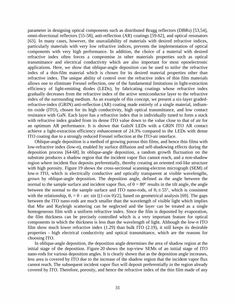
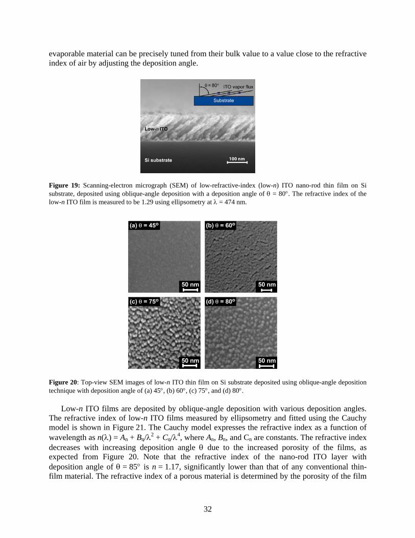
parameter in designing optical components such as distributed Bragg reflectors (DBRs) [53,54], omni-directional reflectors [55-58], anti-reflection (AR) coatings [59-62], and optical resonators [63]. In many cases, however, the unavailability of materials with desired refractive indices, particularly materials with very low refractive indices, prevents the implementation of optical components with very high performance. In addition, the choice of a material with desired refractive index often forces a compromise in other materials properties such as optical transmittance and electrical conductivity which are also important for most optoelectronic applications. Here, we show that oblique-angle deposition can be used to tailor the refractive index of a thin-film material which is chosen for its desired material properties other than refractive index. The unique ability of control over the refractive index of thin film materials allows one to eliminate Fresnel reflection, one of the fundamental limitations in light-extraction efficiency of light-emitting diodes (LEDs), by fabricating coatings whose refractive index gradually decreases from the refractive index of the active semiconductor layer to the refractive index of the surrounding medium. As an example of this concept, we present a six-layer graded-refractive-index (GRIN) anti-reflection (AR) coating made entirely of a single material, indium-tin oxide (ITO), chosen for its high conductivity, high optical transmittance, and low contact resistance with GaN. Each layer has a refractive index that is individually tuned to form a stack with refractive index graded from its dense ITO value down to the value close to that of air for an optimum AR performance. It is shown that GaInN LEDs with a GRIN ITO AR contact achieve a light-extraction efficiency enhancement of 24.3% compared to the LEDs with dense ITO coating due to a strongly reduced Fresnel reflection at the ITO-air interface. Oblique-angle deposition is a method of growing porous thin films, and hence thin films with low-refractive index (low-n), enabled by surface diffusion and self-shadowing effects during the deposition process [64-68]. In oblique-angle deposition, a random growth fluctuation on the substrate produces a shadow region that the incident vapor flux cannot reach, and a non-shadow region where incident flux deposits preferentially, thereby creating an oriented rod-like structure with high porosity. Figure 19 shows the cross-sectional scanning-electron micrograph (SEM) of low-n ITO, which is electrically conductive and optically transparent at visible wavelengths, grown by oblique-angle deposition. The deposition angle, defined as the angle between the normal to the sample surface and incident vapor flux, of = 80 results in the tilt angle, the angle between the normal to the sample surface and ITO nano-rods, of t 55, which is consistent with the relationship, t = - arc sin [(1-cos )/2], based on geometrical analysis [69]. The gaps between the ITO nano-rods are much smaller than the wavelength of visible light which implies that Mie and Rayleigh scattering can be neglected and the layer can be treated as a single homogeneous film with a uniform refractive index. Since the film is deposited by evaporation, the film thickness can be precisely controlled which is a very important feature for optical components in which the thickness is less than the wavelength of light. Although the low-n ITO film show much lower refractive index (1.29) than bulk ITO (2.19), it still keeps its desirable properties - high electrical conductivity and optical transmittance, which are the reasons for choosing ITO. In oblique-angle deposition, the deposition angle determines the area of shadow region at the initial stage of the deposition. Figure 20 shows the top-view SEMs of an initial stage of ITO nano-rods for various deposition angles. It is clearly shown that as the deposition angle increases, less area is covered by ITO due to the increase of the shadow region that the incident vapor flux cannot reach. The subsequent incident vapor flux will deposit preferentially in the region already covered by ITO. Therefore, porosity, and hence the refractive index of the thin film made of any
32
evaporable material can be precisely tuned from their bulk value to a value close to the refractive index of air by adjusting the deposition angle.
Figure 19: Scanning-electron micrograph (SEM) of low-refractive-index (low-n) ITO nano-rod thin film on Si substrate, deposited using oblique-angle deposition with a deposition angle of = 80. The refractive index of the low-n ITO film is measured to be 1.29 using ellipsometry at = 474 nm.
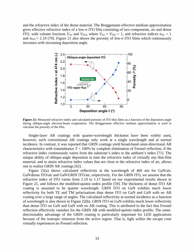
Figure 20: Top-view SEM images of low-n ITO thin film on Si substrate deposited using oblique-angle deposition technique with deposition angle of (a) 45, (b) 60, (c) 75, and (d) 80. Low-n ITO films are deposited by oblique-angle deposition with various deposition angles. The refractive index of low-n ITO films measured by ellipsometry and fitted using the Cauchy model is shown in Figure 21. The Cauchy model expresses the refractive index as a function of wavelength as n() = An + Bn/2 + Cn/ 4, where An, Bn, and Cn are constants. The refractive index decreases with increasing deposition angle due to the increased porosity of the films, as expected from Figure 20. Note that the refractive index of the nano-rod ITO layer with deposition angle of = 85 is n = 1.17, significantly lower than that of any conventional thin-film material. The refractive index of a porous material is determined by the porosity of the film
33
and the refractive index of the dense material. The Bruggemann effective medium approximation gives effective refractive index of a low-n ITO film consisting of two components, air and dense ITO, with volume fractions VAir and VITO, where VAir + VITO = 1, and refractive indices nAir = 1 and nITO = 2.19 [70]. Figure 21 also shows the porosity of low-n ITO films which continuously increases with increasing deposition angle.
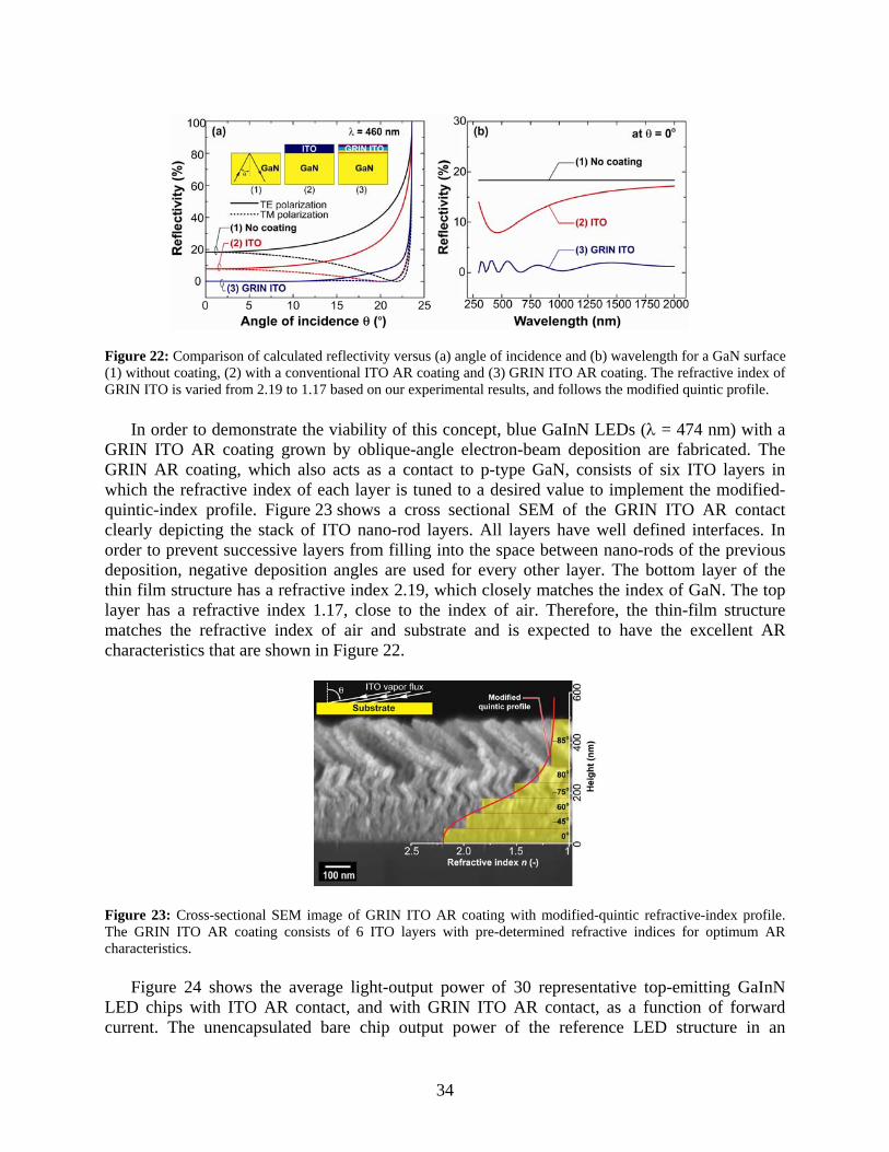
Figure 21: Measured refractive index and calculated porosity of ITO thin films as a function of the deposition angle during oblique-angle electron-beam evaporation. The Bruggemann effective medium approximation is used to calculate the porosity of the film. Single-layer AR coatings with quarter-wavelength thickness have been widely used, however, such conventional AR coatings only work at a single wavelength and at normal incidence. In contrast, it was reported that GRIN coatings yield broad-band omni-directional AR characteristics with transmittance T = 100% by complete elimination of Fresnel reflection, if the refractive index continuously varies from the substrate’s index to the ambient’s index [71]. The unique ability of oblique-angle deposition to tune the refractive index of virtually any thin-film material, and to attain refractive index values that are close to the refractive index of air, allows one to realize GRIN AR coatings [62]. Figure 22(a) shows calculated reflectivity at the wavelength of 460 nm for GaN/air, GaN/dense ITO/air and GaN/GRIN ITO/air, respectively. For the GRIN ITO, we assume that the refractive index of ITO varies from 2.19 to 1.17 based on our experimental results shown in Figure 21, and follows the modified-quintic-index profile [59]. The thickness of dense ITO AR coating is assumed to be quarter wavelength. GRIN ITO on GaN exhibits much lower reflectivity for both TE and TM polarizations than dense ITO on GaN and GaN with no AR coating over a large range of angles. The calculated reflectivity at normal incidence as a function of wavelength is also shown in Figure 22(b). GRIN ITO on GaN exhibits much lower reflectivity than dense ITO on GaN and GaN with no AR coating. This is attributed to the fact that Fresnel reflection effectively vanishes for the GRIN AR with modified-quintic-index profile. The omni-directionality advantage of the GRIN coating is particularly important for LED applications because of the isotropic emission from the active region. That is, light within the escape cone virtually experiences no Fresnel reflection.
34
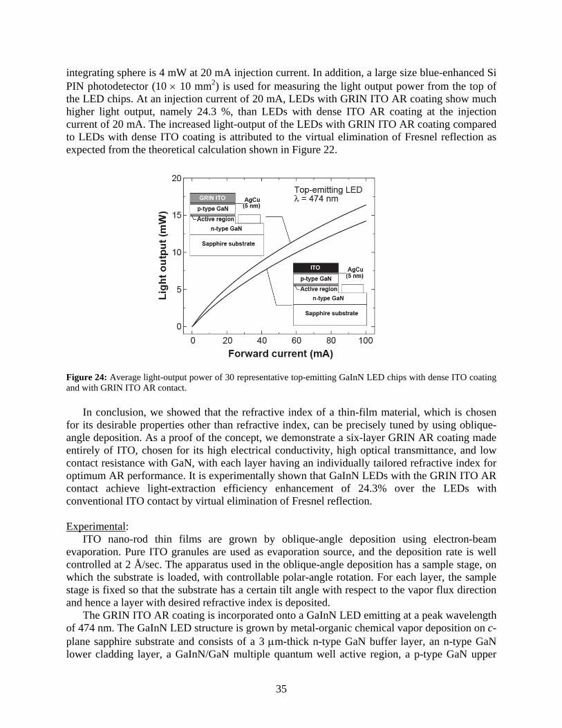
Figure 22: Comparison of calculated reflectivity versus (a) angle of incidence and (b) wavelength for a GaN surface (1) without coating, (2) with a conventional ITO AR coating and (3) GRIN ITO AR coating. The refractive index of GRIN ITO is varied from 2.19 to 1.17 based on our experimental results, and follows the modified quintic profile. In order to demonstrate the viability of this concept, blue GaInN LEDs ( = 474 nm) with a GRIN ITO AR coating grown by oblique-angle electron-beam deposition are fabricated. The GRIN AR coating, which also acts as a contact to p-type GaN, consists of six ITO layers in which the refractive index of each layer is tuned to a desired value to implement the modified-quintic-index profile. Figure 23 shows a cross sectional SEM of the GRIN ITO AR contact clearly depicting the stack of ITO nano-rod layers. All layers have well defined interfaces. In order to prevent successive layers from filling into the space between nano-rods of the previous deposition, negative deposition angles are used for every other layer. The bottom layer of the thin film structure has a refractive index 2.19, which closely matches the index of GaN. The top layer has a refractive index 1.17, close to the index of air. Therefore, the thin-film structure matches the refractive index of air and substrate and is expected to have the excellent AR characteristics that are shown in Figure 22.
Figure 23: Cross-sectional SEM image of GRIN ITO AR coating with modified-quintic refractive-index profile. The GRIN ITO AR coating consists of 6 ITO layers with pre-determined refractive indices for optimum AR characteristics. Figure 24 shows the average light-output power of 30 representative top-emitting GaInN LED chips with ITO AR contact, and with GRIN ITO AR contact, as a function of forward current. The unencapsulated bare chip output power of the reference LED structure in an
35
integrating sphere is 4 mW at 20 mA injection current. In addition, a large size blue-enhanced Si PIN photodetector (10 10 mm2) is used for measuring the light output power from the top of the LED chips. At an injection current of 20 mA, LEDs with GRIN ITO AR coating show much higher light output, namely 24.3 %, than LEDs with dense ITO AR coating at the injection current of 20 mA. The increased light-output of the LEDs with GRIN ITO AR coating compared to LEDs with dense ITO coating is attributed to the virtual elimination of Fresnel reflection as expected from the theoretical calculation shown in Figure 22.
Figure 24: Average light-output power of 30 representative top-emitting GaInN LED chips with dense ITO coating and with GRIN ITO AR contact. In conclusion, we showed that the refractive index of a thin-film material, which is chosen for its desirable properties other than refractive index, can be precisely tuned by using oblique-angle deposition. As a proof of the concept, we demonstrate a six-layer GRIN AR coating made entirely of ITO, chosen for its high electrical conductivity, high optical transmittance, and low contact resistance with GaN, with each layer having an individually tailored refractive index for optimum AR performance. It is experimentally shown that GaInN LEDs with the GRIN ITO AR contact achieve light-extraction efficiency enhancement of 24.3% over the LEDs with conventional ITO contact by virtual elimination of Fresnel reflection. Experimental: ITO nano-rod thin films are grown by oblique-angle deposition using electron-beam evaporation. Pure ITO granules are used as evaporation source, and the deposition rate is well controlled at 2 Å/sec. The apparatus used in the oblique-angle deposition has a sample stage, on which the substrate is loaded, with controllable polar-angle rotation. For each layer, the sample stage is fixed so that the substrate has a certain tilt angle with respect to the vapor flux direction and hence a layer with desired refractive index is deposited. The GRIN ITO AR coating is incorporated onto a GaInN LED emitting at a peak wavelength of 474 nm. The GaInN LED structure is grown by metal-organic chemical vapor deposition on c-plane sapphire substrate and consists of a 3 m-thick n-type GaN buffer layer, an n-type GaN lower cladding layer, a GaInN/GaN multiple quantum well active region, a p-type GaN upper
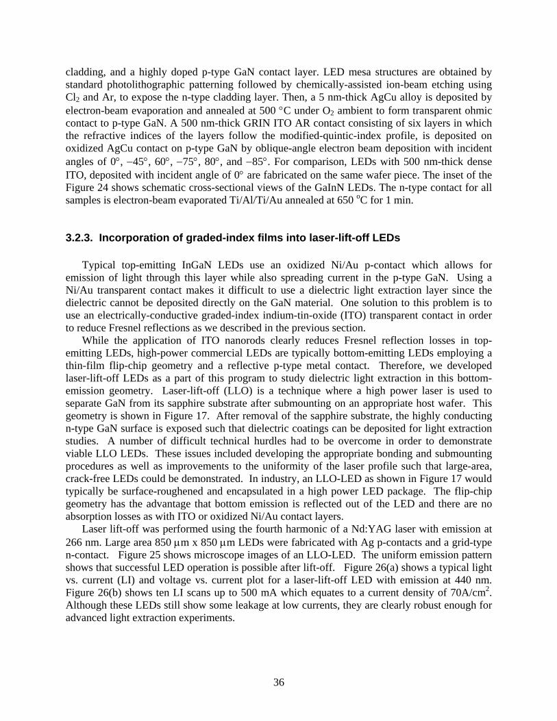
36
cladding, and a highly doped p-type GaN contact layer. LED mesa structures are obtained by standard photolithographic patterning followed by chemically-assisted ion-beam etching using Cl2 and Ar, to expose the n-type cladding layer. Then, a 5 nm-thick AgCu alloy is deposited by electron-beam evaporation and annealed at 500 C under O2 ambient to form transparent ohmic contact to p-type GaN. A 500 nm-thick GRIN ITO AR contact consisting of six layers in which the refractive indices of the layers follow the modified-quintic-index profile, is deposited on oxidized AgCu contact on p-type GaN by oblique-angle electron beam deposition with incident angles of 0, 45, 60, 75, 80, and 85. For comparison, LEDs with 500 nm-thick dense ITO, deposited with incident angle of 0 are fabricated on the same wafer piece. The inset of the Figure 24 shows schematic cross-sectional views of the GaInN LEDs. The n-type contact for all samples is electron-beam evaporated Ti/Al/Ti/Au annealed at 650 oC for 1 min. 3.2.3. Incorporation of graded-index films into laser-lift-off LEDs Typical top-emitting InGaN LEDs use an oxidized Ni/Au p-contact which allows for emission of light through this layer while also spreading current in the p-type GaN. Using a Ni/Au transparent contact makes it difficult to use a dielectric light extraction layer since the dielectric cannot be deposited directly on the GaN material. One solution to this problem is to use an electrically-conductive graded-index indium-tin-oxide (ITO) transparent contact in order to reduce Fresnel reflections as we described in the previous section. While the application of ITO nanorods clearly reduces Fresnel reflection losses in top-emitting LEDs, high-power commercial LEDs are typically bottom-emitting LEDs employing a thin-film flip-chip geometry and a reflective p-type metal contact. Therefore, we developed laser-lift-off LEDs as a part of this program to study dielectric light extraction in this bottom-emission geometry. Laser-lift-off (LLO) is a technique where a high power laser is used to separate GaN from its sapphire substrate after submounting on an appropriate host wafer. This geometry is shown in Figure 17. After removal of the sapphire substrate, the highly conducting n-type GaN surface is exposed such that dielectric coatings can be deposited for light extraction studies. A number of difficult technical hurdles had to be overcome in order to demonstrate viable LLO LEDs. These issues included developing the appropriate bonding and submounting procedures as well as improvements to the uniformity of the laser profile such that large-area, crack-free LEDs could be demonstrated. In industry, an LLO-LED as shown in Figure 17 would typically be surface-roughened and encapsulated in a high power LED package. The flip-chip geometry has the advantage that bottom emission is reflected out of the LED and there are no absorption losses as with ITO or oxidized Ni/Au contact layers. Laser lift-off was performed using the fourth harmonic of a Nd:YAG laser with emission at 266 nm. Large area 850 m x 850 m LEDs were fabricated with Ag p-contacts and a grid-type n-contact. Figure 25 shows microscope images of an LLO-LED. The uniform emission pattern shows that successful LED operation is possible after lift-off. Figure 26(a) shows a typical light vs. current (LI) and voltage vs. current plot for a laser-lift-off LED with emission at 440 nm. Figure 26(b) shows ten LI scans up to 500 mA which equates to a current density of 70A/cm2. Although these LEDs still show some leakage at low currents, they are clearly robust enough for advanced light extraction experiments.
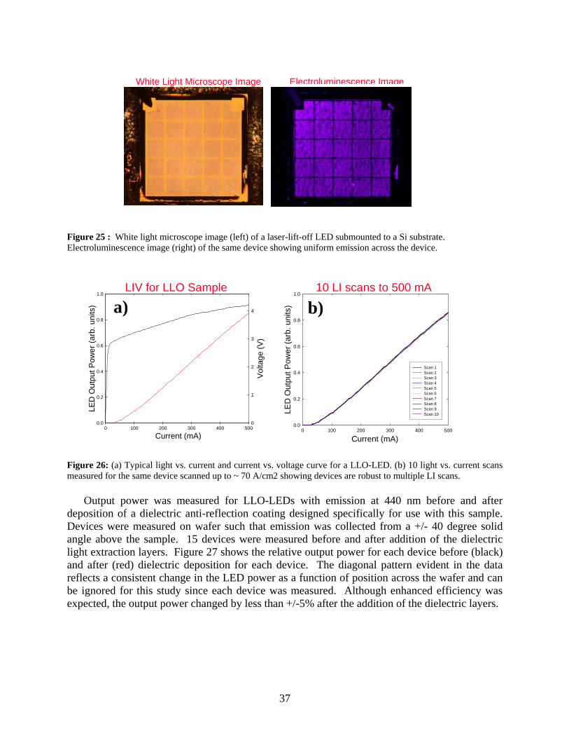
37
Figure 25 : White light microscope image (left) of a laser-lift-off LED submounted to a Si substrate. Electroluminescence image (right) of the same device showing uniform emission across the device.
Figure 26: (a) Typical light vs. current and current vs. voltage curve for a LLO-LED. (b) 10 light vs. current scans measured for the same device scanned up to ~ 70 A/cm2 showing devices are robust to multiple LI scans.
Output power was measured for LLO-LEDs with emission at 440 nm before and after deposition of a dielectric anti-reflection coating designed specifically for use with this sample. Devices were measured on wafer such that emission was collected from a +/- 40 degree solid angle above the sample. 15 devices were measured before and after addition of the dielectric light extraction layers. Figure 27 shows the relative output power for each device before (black) and after (red) dielectric deposition for each device. The diagonal pattern evident in the data reflects a consistent change in the LED power as a function of position across the wafer and can be ignored for this study since each device was measured. Although enhanced efficiency was expected, the output power changed by less than +/-5% after the addition of the dielectric layers.
Current (mA)0 100 200 300 400 500
LED
Out
put P
ower
(a
rb. u
nits
)
0.0
0.2
0.4
0.6
0.8
1.0
Scan 1Scan 2Scan 3Scan 4Scan 5Scan 6Scan 7Scan 8Scan 9Scan 10
10 LI scans to 500 mA
Current (mA)0 100 200 300 400 500
LE
D O
utp
ut P
owe
r (a
rb. u
nits
)
0.0
0.2
0.4
0.6
0.8
1.0
Vol
tage
(V
)
0
1
2
3
4 b)a) LIV for LLO Sample
Electroluminescence ImageWhite Light Microscope Image
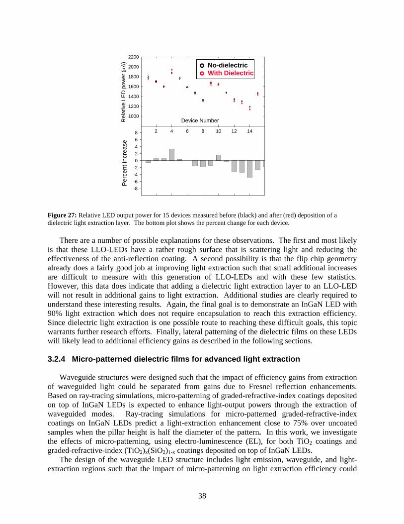
38
Figure 27: Relative LED output power for 15 devices measured before (black) and after (red) deposition of a dielectric light extraction layer. The bottom plot shows the percent change for each device. There are a number of possible explanations for these observations. The first and most likely is that these LLO-LEDs have a rather rough surface that is scattering light and reducing the effectiveness of the anti-reflection coating. A second possibility is that the flip chip geometry already does a fairly good job at improving light extraction such that small additional increases are difficult to measure with this generation of LLO-LEDs and with these few statistics. However, this data does indicate that adding a dielectric light extraction layer to an LLO-LED will not result in additional gains to light extraction. Additional studies are clearly required to understand these interesting results. Again, the final goal is to demonstrate an InGaN LED with 90% light extraction which does not require encapsulation to reach this extraction efficiency. Since dielectric light extraction is one possible route to reaching these difficult goals, this topic warrants further research efforts. Finally, lateral patterning of the dielectric films on these LEDs will likely lead to additional efficiency gains as described in the following sections. 3.2.4 Micro-patterned dielectric films for advanced light extraction Waveguide structures were designed such that the impact of efficiency gains from extraction of waveguided light could be separated from gains due to Fresnel reflection enhancements. Based on ray-tracing simulations, micro-patterning of graded-refractive-index coatings deposited on top of InGaN LEDs is expected to enhance light-output powers through the extraction of waveguided modes. Ray-tracing simulations for micro-patterned graded-refractive-index coatings on InGaN LEDs predict a light-extraction enhancement close to 75% over uncoated samples when the pillar height is half the diameter of the pattern. In this work, we investigate the effects of micro-patterning, using electro-luminescence (EL), for both TiO2 coatings and graded-refractive-index (TiO2)x(SiO2)1-x coatings deposited on top of InGaN LEDs. The design of the waveguide LED structure includes light emission, waveguide, and light-extraction regions such that the impact of micro-patterning on light extraction efficiency could
Device Number
2 4 6 8 10 12 14
Rel
ativ
e LE
D p
ower
( A
)1000
1200
1400
1600
1800
2000
2200
Per
cent
incr
ease
-8
-6
-4
-2
0
2
4
6
8
No-dielectric With Dielectric
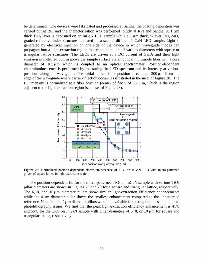
39
be determined. The devices were fabricated and processed at Sandia, the coating deposition was carried out at RPI and the characterization was performed jointly at RPI and Sandia. A 1 m thick TiO2 layer is deposited on an InGaN LED sample while a 1 m thick, 5-layer TiO2-SiO2 graded-refractive-index structure is coated on a second different InGaN LED sample. Light is generated by electrical injection on one side of the device in which waveguide modes can propagate into a light-extraction region that contains pillars of various diameters with square or triangular lattice structures. The LEDs are driven at a DC current of 5 mA and their light emission is collected 50 m above the sample surface via an optical multimode fiber with a core diameter of 105 m which is coupled to an optical spectrometer. Position-dependent electroluminescence is performed by measuring the LED spectrum and its intensity at various positions along the waveguide. The initial optical fiber position is centered 300 m from the edge of the waveguide where carrier-injection occurs, as illustrated in the inset of Figure 28. The EL intensity is normalized at a fiber position (center of fiber) of 350 m, which is the region adjacent to the light-extraction region (see inset of Figure 28).
Figure 28: Normalized position-dependent electroluminescence of TiO2 on InGaN LED with micro-patterned pillars of square lattice in light-extraction region. The position-dependent EL for the micro-patterned TiO2 on InGaN sample with various TiO2 pillar diameters are shown in Figures 28 and 29 for a square and triangular lattice, respectively. The 6, 8, and 10 m diameter pillars show similar light-extraction efficiency enhancements while the 4 m diameter pillar shows the smallest enhancement compared to the unpatterned reference. Note that the 2 m diameter pillars were not available for testing on this sample due to photolithography issues. We find that the peak light-extraction efficiency enhancement is 41% and 55% for the TiO2 on InGaN sample with pillar diameters of 6, 8, or 10 m for square and triangular lattice, respectively.
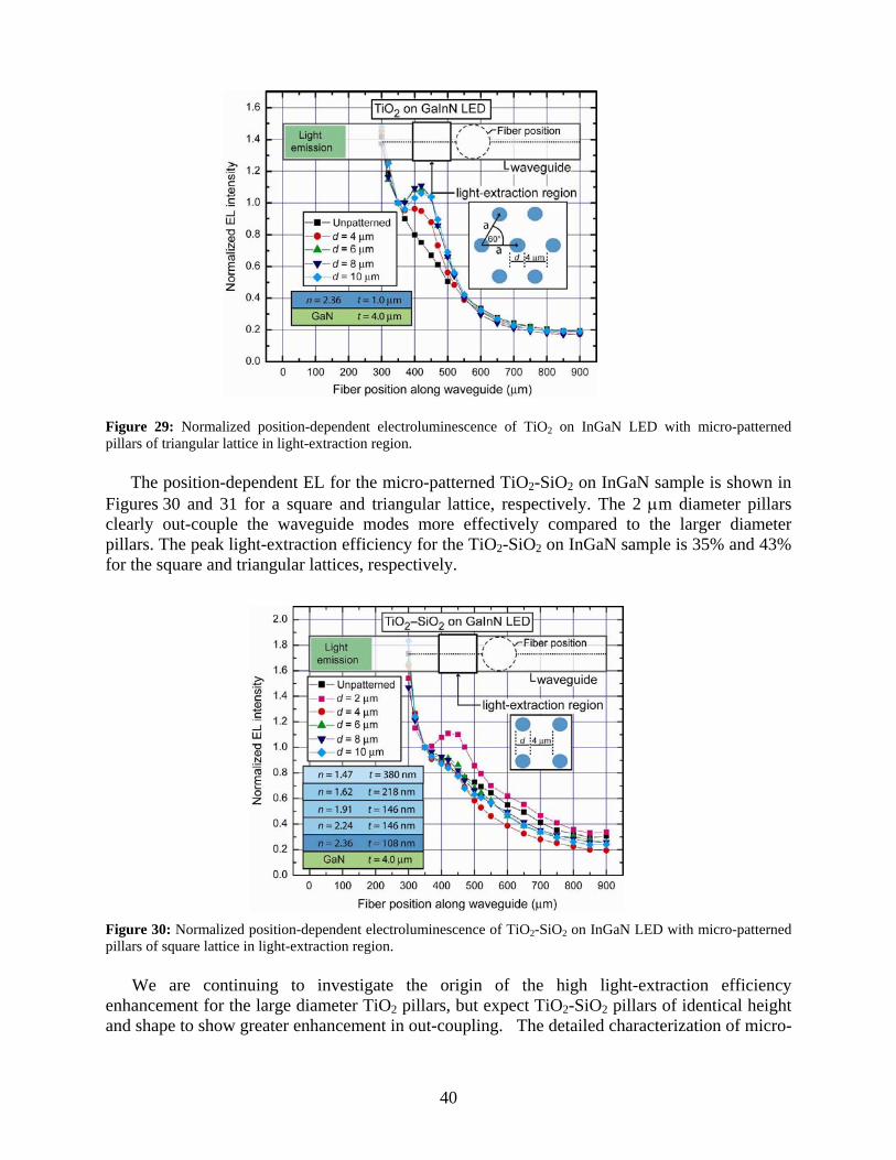
40
Figure 29: Normalized position-dependent electroluminescence of TiO2 on InGaN LED with micro-patterned pillars of triangular lattice in light-extraction region. The position-dependent EL for the micro-patterned TiO2-SiO2 on InGaN sample is shown in Figures 30 and 31 for a square and triangular lattice, respectively. The 2 m diameter pillars clearly out-couple the waveguide modes more effectively compared to the larger diameter pillars. The peak light-extraction efficiency for the TiO2-SiO2 on InGaN sample is 35% and 43% for the square and triangular lattices, respectively.
Figure 30: Normalized position-dependent electroluminescence of TiO2-SiO2 on InGaN LED with micro-patterned pillars of square lattice in light-extraction region. We are continuing to investigate the origin of the high light-extraction efficiency enhancement for the large diameter TiO2 pillars, but expect TiO2-SiO2 pillars of identical height and shape to show greater enhancement in out-coupling. The detailed characterization of micro-
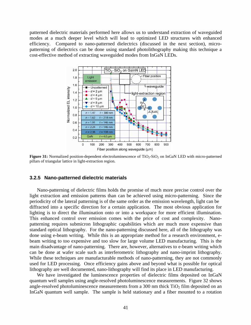
41
patterned dielectric materials performed here allows us to understand extraction of waveguided modes at a much deeper level which will lead to optimized LED structures with enhanced efficiency. Compared to nano-patterned dielectrics (discussed in the next section), micro-patterning of dielectrics can be done using standard photolithography making this technique a cost-effective method of extracting waveguided modes from InGaN LEDs.
Figure 31: Normalized position-dependent electroluminescence of TiO2-SiO2 on InGaN LED with micro-patterned pillars of triangular lattice in light-extraction region. 3.2.5 Nano-patterned dielectric materials
Nano-patterning of dielectric films holds the promise of much more precise control over the light extraction and emission patterns than can be achieved using micro-patterning. Since the periodicity of the lateral patterning is of the same order as the emission wavelength, light can be diffracted into a specific direction for a certain application. The most obvious application for lighting is to direct the illumination onto or into a workspace for more efficient illumination. This enhanced control over emission comes with the price of cost and complexity. Nano-patterning requires submicron lithographic capabilities which are much more expensive than standard optical lithography. For the nano-patterning discussed here, all of the lithography was done using e-beam writing. While this is an appropriate method for a research environment, e-beam writing to too expensive and too slow for large volume LED manufacturing. This is the main disadvantage of nano-patterning. There are, however, alternatives to e-beam writing which can be done at wafer scale such as interferometric lithography and nano-imprint lithography. While these techniques are manufacturable methods of nano-patterning, they are not commonly used for LED processing. Once efficiency gains above and beyond what is possible for optical lithography are well documented, nano-lithography will find its place in LED manufacturing. We have investigated the luminescence properties of dielectric films deposited on InGaN quantum well samples using angle-resolved photoluminescence measurements. Figure 32 shows angle-resolved photoluminescence measurements from a 300 nm thick TiO2 film deposited on an InGaN quantum well sample. The sample is held stationary and a fiber mounted to a rotation
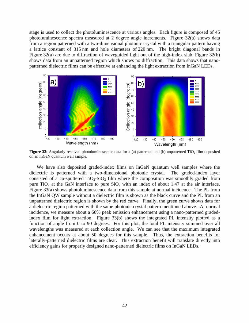
42
stage is used to collect the photoluminescence at various angles. Each figure is composed of 45 photoluminescence spectra measured at 2 degree angle increments. Figure 32(a) shows data from a region patterned with a two-dimensional photonic crystal with a triangular pattern having a lattice constant of 315 nm and hole diameters of 220 nm. The bright diagonal bands in Figure 32(a) are due to diffraction of waveguided light out of the high-index slab. Figure 32(b) shows data from an unpatterned region which shows no diffraction. This data shows that nano-patterned dielectric films can be effective at enhancing the light extraction from InGaN LEDs.
Figure 32: Angularly-resolved photoluminescence data for a (a) patterned and (b) unpatterned TiO2 film deposited on an InGaN quantum well sample. We have also deposited graded-index films on InGaN quantum well samples where the dielectric is patterned with a two-dimensional photonic crystal. The graded-index layer consisted of a co-sputtered TiO2-SiO2 film where the composition was smoothly graded from pure TiO2 at the GaN interface to pure SiO2 with an index of about 1.47 at the air interface. Figure 33(a) shows photoluminescence data from this sample at normal incidence. The PL from the InGaN QW sample without a dielectric film is shown as the black curve and the PL from an unpatterned dielectric region is shown by the red curve. Finally, the green curve shows data for a dielectric region patterned with the same photonic crystal pattern mentioned above. At normal incidence, we measure about a 60% peak emission enhancement using a nano-patterned graded-index film for light extraction. Figure 33(b) shows the integrated PL intensity plotted as a function of angle from 0 to 90 degrees. For this plot, the total PL intensity summed over all wavelengths was measured at each collection angle. We can see that the maximum integrated enhancement occurs at about 50 degrees for this sample. Thus, the extraction benefits for laterally-patterned dielectric films are clear. This extraction benefit will translate directly into efficiency gains for properly designed nano-patterned dielectric films on InGaN LEDs.
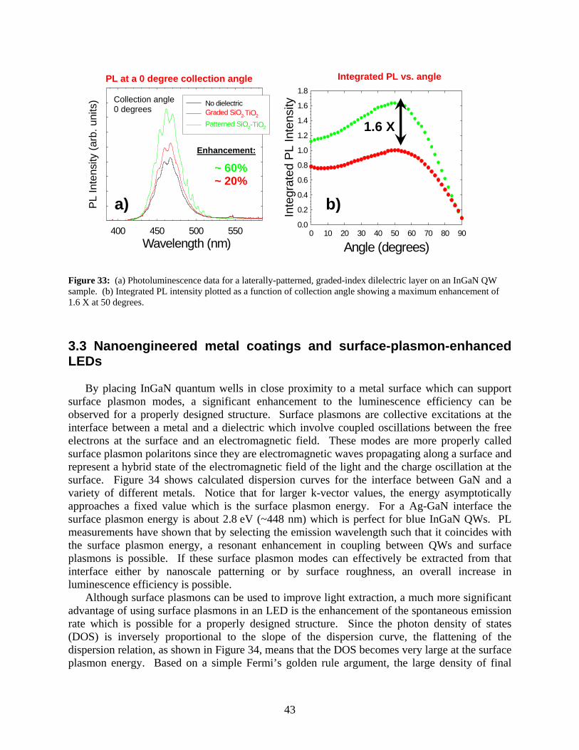
43
Figure 33: (a) Photoluminescence data for a laterally-patterned, graded-index dilelectric layer on an InGaN QW sample. (b) Integrated PL intensity plotted as a function of collection angle showing a maximum enhancement of 1.6 X at 50 degrees.
3.3 Nanoengineered metal coatings and surface-plasmon-enhanced LEDs
By placing InGaN quantum wells in close proximity to a metal surface which can support surface plasmon modes, a significant enhancement to the luminescence efficiency can be observed for a properly designed structure. Surface plasmons are collective excitations at the interface between a metal and a dielectric which involve coupled oscillations between the free electrons at the surface and an electromagnetic field. These modes are more properly called surface plasmon polaritons since they are electromagnetic waves propagating along a surface and represent a hybrid state of the electromagnetic field of the light and the charge oscillation at the surface. Figure 34 shows calculated dispersion curves for the interface between GaN and a variety of different metals. Notice that for larger k-vector values, the energy asymptotically approaches a fixed value which is the surface plasmon energy. For a Ag-GaN interface the surface plasmon energy is about 2.8 eV (~448 nm) which is perfect for blue InGaN QWs. PL measurements have shown that by selecting the emission wavelength such that it coincides with the surface plasmon energy, a resonant enhancement in coupling between QWs and surface plasmons is possible. If these surface plasmon modes can effectively be extracted from that interface either by nanoscale patterning or by surface roughness, an overall increase in luminescence efficiency is possible.
Although surface plasmons can be used to improve light extraction, a much more significant advantage of using surface plasmons in an LED is the enhancement of the spontaneous emission rate which is possible for a properly designed structure. Since the photon density of states (DOS) is inversely proportional to the slope of the dispersion curve, the flattening of the dispersion relation, as shown in Figure 34, means that the DOS becomes very large at the surface plasmon energy. Based on a simple Fermi’s golden rule argument, the large density of final
Angle (degrees)0 10 20 30 40 50 60 70 80 90
Inte
grat
ed P
L In
tens
ity
0.0
0.2
0.4
0.6
0.8
1.0
1.2
1.4
1.6
1.8
1.6 X
Integrated PL vs. angle PL at a 0 degree collection angle
Wavelength (nm)400 450 500 550
PL
Inte
nsity
(ar
b. u
nits
) No dielectricGraded SiO2-TiO2
Patterned SiO2-TiO2
Collection angle 0 degrees
~ 20%
Enhancement:
~ 60%
a) b)
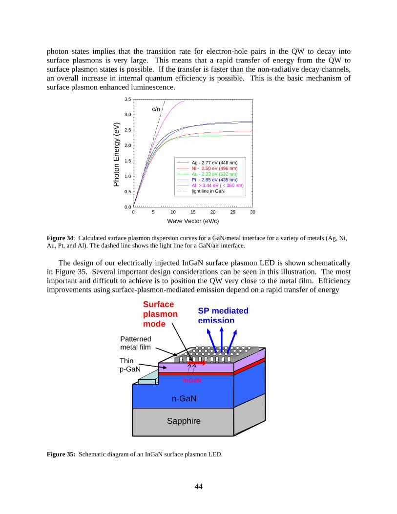
44
photon states implies that the transition rate for electron-hole pairs in the QW to decay into surface plasmons is very large. This means that a rapid transfer of energy from the QW to surface plasmon states is possible. If the transfer is faster than the non-radiative decay channels, an overall increase in internal quantum efficiency is possible. This is the basic mechanism of surface plasmon enhanced luminescence.
Figure 34: Calculated surface plasmon dispersion curves for a GaN/metal interface for a variety of metals (Ag, Ni, Au, Pt, and Al). The dashed line shows the light line for a GaN/air interface.
The design of our electrically injected InGaN surface plasmon LED is shown schematically in Figure 35. Several important design considerations can be seen in this illustration. The most important and difficult to achieve is to position the QW very close to the metal film. Efficiency improvements using surface-plasmon-mediated emission depend on a rapid transfer of energy
Figure 35: Schematic diagram of an InGaN surface plasmon LED.
Patterned metal film
Thin p-GaN
Surface plasmon mode
SP mediated emission
Sapphire
n-GaN
InGaN
Wave Vector (eV/c)
0 5 10 15 20 25 30
Pho
ton
Ene
rgy
(eV
)
0.0
0.5
1.0
1.5
2.0
2.5
3.0
3.5
Ag - 2.77 eV (448 nm)Ni - 2.50 eV (496 nm)Au - 2.33 eV (532 nm)Pt - 2.85 eV (435 nm)Al > 3.44 eV ( < 360 nm)light line in GaN
c/n
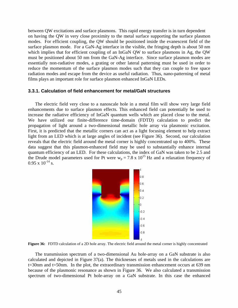
45
between QW excitations and surface plasmons. This rapid energy transfer is in turn dependent on having the QW in very close proximity to the metal surface supporting the surface plasmon modes. For efficient coupling, the QW should be positioned inside the evanescent field of the surface plasmon mode. For a GaN-Ag interface in the visible, the fringing depth is about 50 nm which implies that for efficient coupling of an InGaN QW to surface plasmons in Ag, the QW must be positioned about 50 nm from the GaN-Ag interface. Since surface plasmon modes are essentially non-radiative modes, a grating or other lateral patterning must be used in order to reduce the momentum of the surface plasmon modes such that they can couple to free space radiation modes and escape from the device as useful radiation. Thus, nano-patterning of metal films plays an important role for surface plasmon enhanced InGaN LEDs.
3.3.1. Calculation of field enhancement for metal/GaN structures
The electric field very close to a nanoscale hole in a metal film will show very large field enhancements due to surface plasmon effects. This enhanced field can potentially be used to increase the radiative efficiency of InGaN quantum wells which are placed close to the metal. We have utilized our finite-difference time-domain (FDTD) calculation to predict the propagation of light around a two-dimensional metallic hole array via plasmonic excitation. First, it is predicted that the metallic corners can act as a light focusing element to help extract light from an LED which is at large angles of incident (see Figure 36). Second, our calculation reveals that the electric field around the metal corner is highly concentrated up to 400%. These data suggest that this plasmon-enhanced field may be used to substantially enhance internal quantum efficiency of an LED. For these calculations, the index of GaN was taken to be 2.5 and the Drude model parameters used for Pt were wp = 7.8 x 10¹⁵ Hz and a relaxation frequency of 0.95 x 10⁻¹⁴ s.
Figure 36: FDTD calculation of a 2D hole array. The electric field around the metal corner is highly concentrated The transmission spectrum of a two-dimensional Au hole-array on a GaN substrate is also calculated and depicted in Figure 37(a). The thicknesses of metals used in the calculations are t=30nm and t=50nm. In the plot, the extraordinary transmission enhancement occurs at 639 nm because of the plasmonic resonance as shown in Figure 36. We also calculated a transmission spectrum of two-dimensional Pt hole-array on a GaN substrate. In this case the enhanced
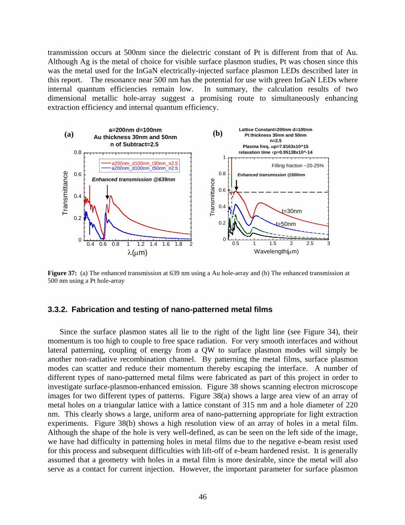
46
transmission occurs at 500nm since the dielectric constant of Pt is different from that of Au. Although Ag is the metal of choice for visible surface plasmon studies, Pt was chosen since this was the metal used for the InGaN electrically-injected surface plasmon LEDs described later in this report. The resonance near 500 nm has the potential for use with green InGaN LEDs where internal quantum efficiencies remain low. In summary, the calculation results of two dimensional metallic hole-array suggest a promising route to simultaneously enhancing extraction efficiency and internal quantum efficiency.
Figure 37: (a) The enhanced transmission at 639 nm using a Au hole-array and (b) The enhanced transmission at 500 nm using a Pt hole-array
3.3.2. Fabrication and testing of nano-patterned metal films
Since the surface plasmon states all lie to the right of the light line (see Figure 34), their momentum is too high to couple to free space radiation. For very smooth interfaces and without lateral patterning, coupling of energy from a QW to surface plasmon modes will simply be another non-radiative recombination channel. By patterning the metal films, surface plasmon modes can scatter and reduce their momentum thereby escaping the interface. A number of different types of nano-patterned metal films were fabricated as part of this project in order to investigate surface-plasmon-enhanced emission. Figure 38 shows scanning electron microscope images for two different types of patterns. Figure 38(a) shows a large area view of an array of metal holes on a triangular lattice with a lattice constant of 315 nm and a hole diameter of 220 nm. This clearly shows a large, uniform area of nano-patterning appropriate for light extraction experiments. Figure 38(b) shows a high resolution view of an array of holes in a metal film. Although the shape of the hole is very well-defined, as can be seen on the left side of the image, we have had difficulty in patterning holes in metal films due to the negative e-beam resist used for this process and subsequent difficulties with lift-off of e-beam hardened resist. It is generally assumed that a geometry with holes in a metal film is more desirable, since the metal will also serve as a contact for current injection. However, the important parameter for surface plasmon
0
0.2
0.4
0.6
0.8
0.4 0.6 0.8 1 1.2 1.4 1.6 1.8 2
a=200nm d=100nmAu thickness 30nm and 50nm
n of Subtract=2.5
a200nm_d100nm_t30nm_n2.5a200nm_d100nm_t50nm_n2.5
Tra
nsm
itta
nce
(m)
Enhanced transmission @639nm
(a)
0
0.2
0.4
0.6
0.8
1
0.5 1 1.5 2 2.5 3
Lattice Constant=200nm d=100nmPt thickness 30nm and 50nm
n=2.5Plasma freq. p=7.8163x10^15
relaxation time p=0.95138x10^-14
Tra
nsm
ittan
ce
Wavelength(m)
t=30nm
t=50nm
Filling fraction ~20-25%
Enhanced transmission @500nm
(b)
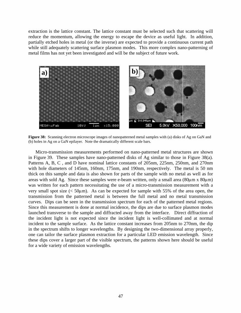
47
extraction is the lattice constant. The lattice constant must be selected such that scattering will reduce the momentum, allowing the energy to escape the device as useful light. In addition, partially etched holes in metal (or the inverse) are expected to provide a continuous current path while still adequately scattering surface plasmon modes. This more complex nano-patterning of metal films has not yet been investigated and will be the subject of future work.
Figure 38: Scanning electron microscope images of nanopatterned metal samples with (a) disks of Ag on GaN and (b) holes in Ag on a GaN epilayer. Note the dramatically different scale bars. Micro-transmission measurements performed on nano-patterned metal structures are shown in Figure 39. These samples have nano-patterned disks of Ag similar to those in Figure 38(a). Patterns A, B, C , and D have nominal lattice constants of 205nm, 225nm, 250nm, and 270nm with hole diameters of 145nm, 160nm, 175nm, and 190nm, respectively. The metal is 50 nm thick on this sample and data is also shown for parts of the sample with no metal as well as for areas with sold Ag. Since these samples were e-beam written, only a small area (80m x 80m) was written for each pattern necessitating the use of a micro-transmission measurement with a very small spot size (< 50m). As can be expected for sample with 55% of the area open, the transmission from the patterned metal is between the full metal and no metal transmission curves. Dips can be seen in the transmission spectrum for each of the patterned metal regions. Since this measurement is done at normal incidence, the dips are due to surface plasmon modes launched transverse to the sample and diffracted away from the interface. Direct diffraction of the incident light is not expected since the incident light is well-collimated and at normal incident to the sample surface. As the lattice constant increases from 205nm to 270nm, the dip in the spectrum shifts to longer wavelengths. By designing the two-dimensional array properly, one can tailor the surface plasmon extraction for a particular LED emission wavelength. Since these dips cover a larger part of the visible spectrum, the patterns shown here should be useful for a wide variety of emission wavelengths.
a) b)
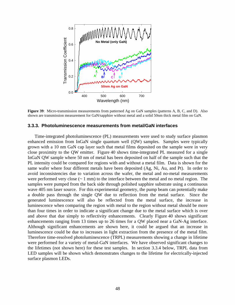
48
Figure 39: Micro-transmission measurements from patterned Ag on GaN samples (patterns A, B, C, and D). Also shown are transmission measurement for GaN/sapphire without metal and a solid 50nm thick metal film on GaN. 3.3.3. Photoluminescence measurements from metal/GaN interfaces Time-integrated photoluminescence (PL) measurements were used to study surface plasmon enhanced emission from InGaN single quantum well (QW) samples. Samples were typically grown with a 10 nm GaN cap layer such that metal films deposited on the sample were in very close proximity to the QW emitter. Figure 40 shows time-integrated PL measured for a single InGaN QW sample where 50 nm of metal has been deposited on half of the sample such that the PL intensity could be compared for regions with and without a metal film. Data is shown for the same wafer where four different metals have been deposited (Ag, Ni, Au, and Pt). In order to avoid inconsistencies due to variation across the wafer, the metal and no-metal measurements were performed very close (~ 1 mm) to the interface between the metal and no metal region. The samples were pumped from the back side through polished sapphire substrate using a continuous wave 405 nm laser source. For this experimental geometry, the pump beam can potentially make a double pass through the single QW due to reflection from the metal surface. Since the generated luminescence will also be reflected from the metal surface, the increase in luminescence when comparing the region with metal to the region without metal should be more than four times in order to indicate a significant change due to the metal surface which is over and above that due simply to reflectivity enhancements. Clearly Figure 40 shows significant enhancements ranging from 13 times up to 26 times for a QW placed near a GaN-Ag interface. Although significant enhancements are shown here, it could be argued that an increase in luminescence could be due to increases in light extraction from the presence of the metal film. Therefore time-resolved photoluminescence (TRPL) measurements showing a change in lifetime were performed for a variety of metal-GaN interfaces. We have observed significant changes to the lifetimes (not shown here) for these test samples. In section 3.3.4 below, TRPL data from LED samples will be shown which demonstrates changes to the lifetime for electrically-injected surface plasmon LEDs.
Wavelength (nm)400 500 600 700
Tra
nsm
issi
on C
oeffi
cien
t
0.0
0.2
0.4
0.6
0.8
A B C D
No Metal (only GaN)
50nm Ag on GaN
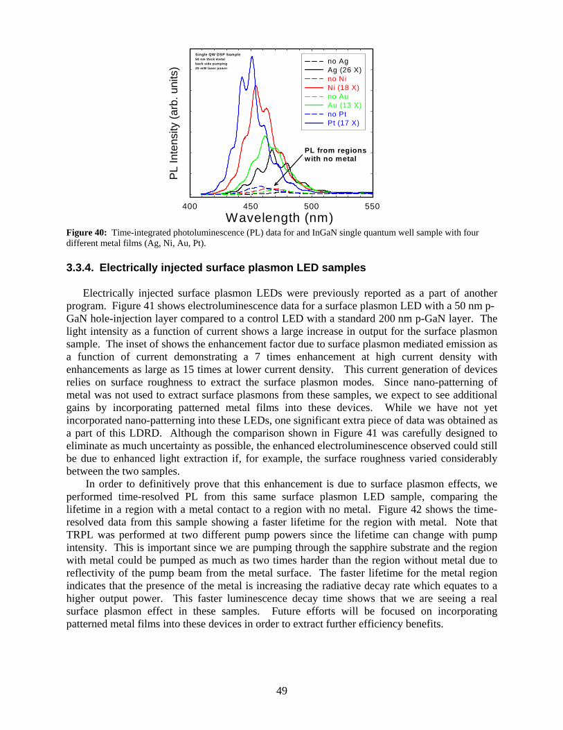
49
Figure 40: Time-integrated photoluminescence (PL) data for and InGaN single quantum well sample with four different metal films (Ag, Ni, Au, Pt). 3.3.4. Electrically injected surface plasmon LED samples Electrically injected surface plasmon LEDs were previously reported as a part of another program. Figure 41 shows electroluminescence data for a surface plasmon LED with a 50 nm p- GaN hole-injection layer compared to a control LED with a standard 200 nm p-GaN layer. The light intensity as a function of current shows a large increase in output for the surface plasmon sample. The inset of shows the enhancement factor due to surface plasmon mediated emission as a function of current demonstrating a 7 times enhancement at high current density with enhancements as large as 15 times at lower current density. This current generation of devices relies on surface roughness to extract the surface plasmon modes. Since nano-patterning of metal was not used to extract surface plasmons from these samples, we expect to see additional gains by incorporating patterned metal films into these devices. While we have not yet incorporated nano-patterning into these LEDs, one significant extra piece of data was obtained as a part of this LDRD. Although the comparison shown in Figure 41 was carefully designed to eliminate as much uncertainty as possible, the enhanced electroluminescence observed could still be due to enhanced light extraction if, for example, the surface roughness varied considerably between the two samples. In order to definitively prove that this enhancement is due to surface plasmon effects, we performed time-resolved PL from this same surface plasmon LED sample, comparing the lifetime in a region with a metal contact to a region with no metal. Figure 42 shows the time-resolved data from this sample showing a faster lifetime for the region with metal. Note that TRPL was performed at two different pump powers since the lifetime can change with pump intensity. This is important since we are pumping through the sapphire substrate and the region with metal could be pumped as much as two times harder than the region without metal due to reflectivity of the pump beam from the metal surface. The faster lifetime for the metal region indicates that the presence of the metal is increasing the radiative decay rate which equates to a higher output power. This faster luminescence decay time shows that we are seeing a real surface plasmon effect in these samples. Future efforts will be focused on incorporating patterned metal films into these devices in order to extract further efficiency benefits.
Wavelength (nm)400 450 500 550
PL
Inte
nsity
(ar
b. u
nits
)
no AgAg (26 X)no NiNi (18 X)no AuAu (13 X)no PtPt (17 X)
Single QW DSP Sample50 nm thick metal
back side pumping
20 mW laser power
PL from regionswith no metal
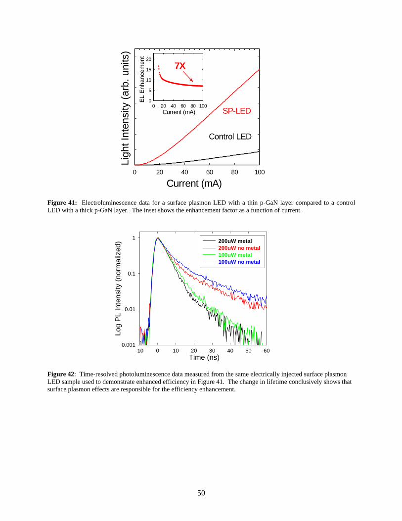
50
Current (mA)0 20 40 60 80 100
Ligh
t Int
ensi
ty (
arb.
uni
ts)
Current (mA)0 20 40 60 80 100
EL
Enh
ance
men
t
0
5
10
15
20
7X
SP-LED
Control LED
Figure 41: Electroluminescence data for a surface plasmon LED with a thin p-GaN layer compared to a control LED with a thick p-GaN layer. The inset shows the enhancement factor as a function of current.
Figure 42: Time-resolved photoluminescence data measured from the same electrically injected surface plasmon LED sample used to demonstrate enhanced efficiency in Figure 41. The change in lifetime conclusively shows that surface plasmon effects are responsible for the efficiency enhancement.
Time (ns)-10 0 10 20 30 40 50 60
Log
PL
Inte
nsity
(no
rmal
ized
)
0.001
0.01
0.1
1200uW metal 200uW no metal 100uW metal100uW no metal
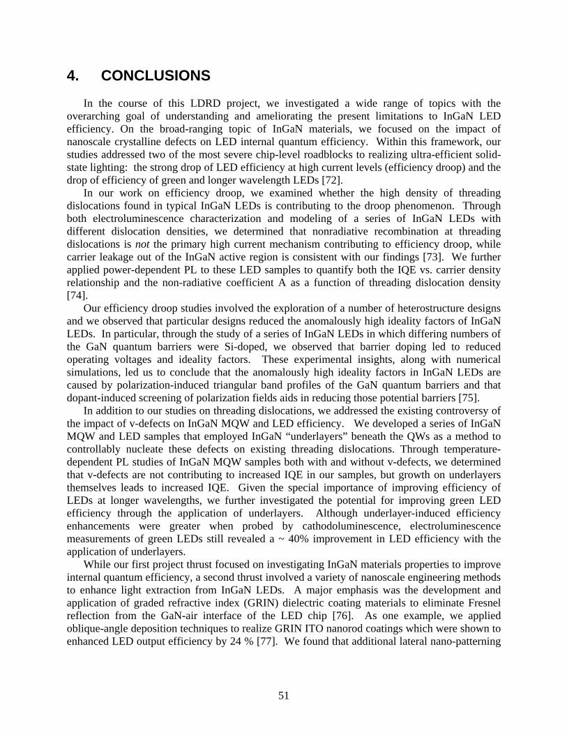
51
4. CONCLUSIONS In the course of this LDRD project, we investigated a wide range of topics with the overarching goal of understanding and ameliorating the present limitations to InGaN LED efficiency. On the broad-ranging topic of InGaN materials, we focused on the impact of nanoscale crystalline defects on LED internal quantum efficiency. Within this framework, our studies addressed two of the most severe chip-level roadblocks to realizing ultra-efficient solid-state lighting: the strong drop of LED efficiency at high current levels (efficiency droop) and the drop of efficiency of green and longer wavelength LEDs [72]. In our work on efficiency droop, we examined whether the high density of threading dislocations found in typical InGaN LEDs is contributing to the droop phenomenon. Through both electroluminescence characterization and modeling of a series of InGaN LEDs with different dislocation densities, we determined that nonradiative recombination at threading dislocations is not the primary high current mechanism contributing to efficiency droop, while carrier leakage out of the InGaN active region is consistent with our findings [73]. We further applied power-dependent PL to these LED samples to quantify both the IQE vs. carrier density relationship and the non-radiative coefficient A as a function of threading dislocation density [74]. Our efficiency droop studies involved the exploration of a number of heterostructure designs and we observed that particular designs reduced the anomalously high ideality factors of InGaN LEDs. In particular, through the study of a series of InGaN LEDs in which differing numbers of the GaN quantum barriers were Si-doped, we observed that barrier doping led to reduced operating voltages and ideality factors. These experimental insights, along with numerical simulations, led us to conclude that the anomalously high ideality factors in InGaN LEDs are caused by polarization-induced triangular band profiles of the GaN quantum barriers and that dopant-induced screening of polarization fields aids in reducing those potential barriers [75]. In addition to our studies on threading dislocations, we addressed the existing controversy of the impact of v-defects on InGaN MQW and LED efficiency. We developed a series of InGaN MQW and LED samples that employed InGaN “underlayers” beneath the QWs as a method to controllably nucleate these defects on existing threading dislocations. Through temperature-dependent PL studies of InGaN MQW samples both with and without v-defects, we determined that v-defects are not contributing to increased IQE in our samples, but growth on underlayers themselves leads to increased IQE. Given the special importance of improving efficiency of LEDs at longer wavelengths, we further investigated the potential for improving green LED efficiency through the application of underlayers. Although underlayer-induced efficiency enhancements were greater when probed by cathodoluminescence, electroluminescence measurements of green LEDs still revealed a ~ 40% improvement in LED efficiency with the application of underlayers. While our first project thrust focused on investigating InGaN materials properties to improve internal quantum efficiency, a second thrust involved a variety of nanoscale engineering methods to enhance light extraction from InGaN LEDs. A major emphasis was the development and application of graded refractive index (GRIN) dielectric coating materials to eliminate Fresnel reflection from the GaN-air interface of the LED chip [76]. As one example, we applied oblique-angle deposition techniques to realize GRIN ITO nanorod coatings which were shown to enhanced LED output efficiency by 24 % [77]. We found that additional lateral nano-patterning
52
and micro-patterning of GRIN dielectric layers helps to the extract waveguided modes and leads to even higher efficiencies. Beyond dielectric materials, we also investigated nanostructured metal coatings and the potential for surface-plasmon-induced improvements to LED efficiency. Our studies confirmed strong photoluminescence enhancement from InGaN QWs with various metal coatings and further demonstrated both enhanced LED output and reduced PL lifetimes of LEDs employing metal coatings in close proximity to QW layers. We note that while the main focus of this thrust area was to explore methods to enhance light extraction, the coupling of QW excitation to surface plasmon modes in nearby metal coating layers is likely most advantageous in its potential to increase internal quantum efficiency of InGaN LEDs rather than light extraction. Thus, surface-plasmon-enhanced emission is most promising for LEDs that presently have low internal quantum efficiencies, including green and longer wavelength LEDs. In summary, our joint SNL/RPI project has yielded a number of valuable insights and direct demonstrations of approaches to improve internal quantum efficiency and extraction efficiency of InGaN-based LEDs. These results indicate the continued importance of both nanoscale materials studies and nanoscale engineering of materials to maximize LED efficiencies and to realize ultra-efficient solid-state lighting.
53
5. REFERENCES 1. M. R. Krames, O. B. Shchekin, R. Mueller-Mach, G. O. Mueller, L. Zhou, G. Harbers, and
M. George Craford, J. Displ. Technol. 3, 160 (2007). 2. I. V. Rozhansky and D. A. Zakheim, Phys. Stat. Sol. (c) 3, 2160-2164 (2006). 3. I. V. Rozhansky and D. A. Zakheim, Phys. Stat. Sol. (a) 204, 227-230 (2007). 4. M. H. Kim, M. F. Schubert, Q. Dai, J. K. Kim, E. F. Schubert, J. Piprek, and Y. Park, Appl.
Phys. Lett. 91, 183507 (2007). 5. Y. C. Shen, G. O. Mueller, S. Watanabe, N. F. Gardner, A. Munkholm, and M. R. Krames,
Appl. Phys. Lett. 91, 141101 (2007). 6. A. A. Efremov, N. I. Bochkareva, R. I. Gorbunov, D. A. Larinovich, Yu. T. Rebane, D. V.
Tarkhin, and Yu. G. Shreter, Semiconductors 40, 605-610 (2006). 7. A. Y. Kim, W. Götz, D.A. Steigerwald, J. J. Wierer, N. F. Gardner, J. Sun, S. A. Stockman,
P. S. Martin, M. R. Krames, R. S. Kern, and F. M. Steranka, Phys. Stat. Sol. (a) 188, 15 (2001).
8. S. F. Chichibu, T. Azuhata, M. Sugiyama, T. Kitamura, Y. Ishida, H. Okumurac, H. Nakanishi, T. Sota, T. Mukai, J. Vac. Sci. Technol. B 19, 2177 (2001).
9. K. Akita, T. Kyono, Y. Yoshizumi, H. Kitabayashi, and K. Katayama, J. Appl. Phys. 101, 033104 (2007).
10. D. D. Koleske, A. J. Fischer, A. A. Allerman, C. C. Mitchell, K. C. Cross, S. R. Kurtz, J. J. Figiel, K. W. Fullmer, and W. G. Breiland, Appl. Phys. Lett. 81, 1940 (2002).
11. D. D. Koleske and S. R. Lee, manuscript in preparation. 12. S. R. Lee, A. M. West, A. A. Allerman, K. E. Waldrip, D. M. Follstaedt, P. P. Provencio, D.
D. Koleske, and C. R. Abernathy, Appl. Phys. Lett. 86, 241904 (2005). 13. W. G. Breiland and K. P. Killeen, J. Appl. Phys. 78, 6726 (1995). 14. E. F. Schubert, Light-Emitting Diodes, second edition, (Cambridge University Press,
Cambridge 2006). 15. T. Fleck, M. Schmidt, and C. Klingshirn, Phys. Stat. Sol. (a) 198, 248 (2003). 16. H. Gauck, T. H. Gfroerer, M. J. Renn, E. A. Cornell, and K. A. Bertness, Appl. Phys. A 64,
143 (1997). 17. R. K. Ahrenkiel, Solid-State Electronics 35, 239 (1992). 18. C. E. Martinez, N. M. Stanton, A. J. Kent, D. M. Graham, P. Dawson, M. J. Kappers, and
C. J. Humphreys, J. Appl. Phys. 98, 053509 (2005). 19. S. Watanabe, N. Yamada, M. Nagashima, Y. Ueki, C. Sasaki, Y. Yamada, T. Taguchi,
K. Tadatomo, H. Okagawa, and H. Kudo, Appl. Phys. Lett. 83, 4906 (2003). 20. D. Ding, S. R. Johnson, J. B. Wang, S. Q. Yu, and Y. H. Zhang, Proc. SPIE 6841, 68410D,
(2007). 21. H. Y. Ryu, K. H. Ha, J. H. Chae, K. S. Kim, J. K. Son, O. H. Nam, Y. J. Park, and J. I. Shim,
Appl. Phys. Lett. 89, 171106 (2006). 22. G. B. Ren, H. Summers, P. Blood, R. Perks, and D. Bour, Proc. SPIE 4283, 78 (2001). 23. M. H. Kim, M. F. Schubert, Q. Dai, J. K. Kim, E. F. Schubert, J. Piprek, and Y. Park, Appl.
Phys. Lett. 91,183507 (2007). 24. M. F. Schubert, S. Chhajed, J. K. Kim, E. F. Schubert, D. D. Koleske, M. H. Crawford, S. R.
Lee, A. J. Fischer, G. Thaler, and M. A. Banas, Appl. Phys. Lett. 91, 231114 (2007). 25. X. Ni, Q. Fan, R. Shimada, U. Ozgur, and H. Morkoc, Appl. Phys. Lett. 93, 171113 (2008)
54
26. D. D. Koleske, A. J. Fischer, A. A. Allerman, C. C. Mitchell, K. C. Cross, S. R. Kurtz, J. J. Figiel, K. W. Fullmer, and W. G. Breiland, Appl. Phys. Lett. 81, 1940 (2002).
27. D. D. Koleske and S. R. Lee (unpublished). 28. S. R. Lee, A. M. West, A. A. Allerman, K. E. Waldrip, D. M. Follstaedt, P. P. Provencio, D.
D. Koleske, and C. R. Abernathy, Appl. Phys. Lett. 86, 241904 (2005). 29. E. F. Schubert, Light-Emitting Diodes, 2nd ed. (Cambridge University Press, Cambridge,
UK, 2006). 30. J. S. Speck and S. J. Rosner, Physica B 273-274, 24 (1999). 31. S. F. Chichibu, H. Marchand, M. S. Minsky, S. Keller, P. T. Fini, J. P. Ibbetson, S. B.
Fleischer, J. S. Speck, J. E. Bowers, E. Hu, U. K. Mishra, S. P. DenBaarrs, T. Deguchi, T. Sota, and S. Nakamura, Appl. Phys. Lett. 74, 1460 (1999).
32. P. G. Eliseev, M. Osin’ski, H. Li, and I. V. Akimova, Appl. Phys. Lett. 75, 3838 (1999). 33. M. F. Schubert, J. Xu, Q. Dai, F. W. Mont, J. K. Kim, and E. F. Schubert, Appl. Phys. Lett.
94,081114 (2009). 34. A. J. Fischer, A. A. Allerman, M. H. Crawford, K. H. A. Bogart, S. R. Lee, R. J. Kaplar, W.
W. Chow, S. R. Kurtz, K. W. Fullmer, and J. J. Figiel, Appl. Phys. Lett. 84, 3394 (2004) 35. M. Koike, N. Shibata, H. Kato, and Y. Takahashi, IEEE J. Sel. Top. Quant. 8, 271 (2002) 36. J. M. Shah, Y. -L. Li, Th. Gessmann, and E. F. Schubert, J. Appl. Phys. 94, 2627 (2003) 37. H. C. Casey, Jr., J. Muth, S. Krishnankutty, and J. M. Zavada, Appl. Phys. Lett. 68, 2867
(1996) 38. P. Perlin, M Osiński, P. G. Eliseev, V. A. Smagley, J. Mu, M. Banas, and P. Sartori, Appl.
Phys. Lett. 69, 1680 (1996) 39. X. A. Cao, E. B. Stokes, P. M. Sandvik, S. F. LeBoeuf, J. Kretchmer, D. Walker, IEEE Elec.
Dev. Lett. 23, 535 (2002) 40. K. Mayes, A. Yasan, R. McClintock, D. Shiell, S. R. Darvish, P. Kung, and M. Razeghi,
Appl. Phys. Lett. 84, 1046 (2004) 41. T. Li, D. J. H. Lambert, M. M. Wong, C. J. Collins, B. Yang, A. L. Beck, U. Chowdhury, R.
D. Dupuis, and J. C. Campbell, IEEE J. Quantum Electron. 37, 538 (2001) 42. C. Sah, R. N. Noyce, and W. Shockley, Proc. IRE 45, 1228 (1957) 43. E. F. Schubert, Light-Emitting Diodes, 2nd ed. (Cambridge University Press, Cambridge,
UK, 2006) 44. G. Martin, A. Botchkarev, A. Rockett, and H. Morkoc, Appl. Phys. Lett. 68, 2541 (1996) 45. S. L. Chuang and C. S. Chang, Semicond. Sci. Technol. 12, 252 (1997) 46. F. Bernardini, V. Fiorentini, and D. Vanderbilt, Phys. Rev. B 56, 10024 (1997) 47. F. Bernardini, in Nitride Semiconductor Devices: Principles and Simulation, edited by J.
Piprek (Wiley-VCH, Weinheim, 2007), pp. 49–67 48. M. F. Schubert, J. Xu, J. K. Kim, E. F. Schubert, M. H. Kim, S. Yoon, S. M. Lee, C. Sone, T.
Sakong, and Y. Park, Appl. Phys. Lett. 93, 041102 (2008). 49. A. Hangleiter, F. Hitzel, C. Netzel, D. Fuhrmann, U. Rossow, G. Ade, and P. Hinze, Phys.
Rev. Lett. 95, 127402 (2005). 50. C. Wetzel and T. Detchprohm, MRS Internet J. Nitride Semicond. Res. 10, 2 (2005), and
references therein. 51. F. Scholz, A. Sohmer, J. Off, V. Syganow, A. Dornen, J.-S. Im, A. Hangleiter and H. Lakner,
Mat. Sci. And Eng. B 50, 238 (1997). 52. J.-Q. Xi, M. F. Schubert, J. K. Kim, E. F. Schubert, M. Chen, S.-Y. Lin, W. Liu and J. A.
Smart, Nat. Photonics 1, 176 (2007).
55
53. R. Sharma, E. D. Haberer, C. Meier, E. L. Hu, S. Nakamura, Appl. Phys. Lett. 87, 051107 (2005).
54. S.-T. Ho, S. L. McCall, R. E. Slusher, L. N. Pfeiffer, K. W. West, A. F. J. Levi, G. E. Blonder, and J. L. Jewell, Appl. Phys. Lett. 57, 1387 (1990).
55. J.-Q. Xi, M. Ojha, J. L. Plawsky, W. N. Gill, J. K. Kim, and E. F. Schubert, Appl. Phys. Lett. 87, 031111 (2005).
56. J.-Q. Xi, M. Ojha, W. Cho, J. L. Plawsky, W. N. Gill, T. Gessmann, and E. F. Schubert, Opt. Lett. 30, 1518 (2005).
57. Jong Kyu Kim, T. Gessmann, E. Fred Schubert, J.-Q. Xi, Hong Luo, J. Cho, C. Sone, Y. Park, Appl. Phys. Lett. 88, 013501 (2006).
58. Jong Kyu Kim, J.-Q. Xi, Hong Luo, E. Fred Schubert, J. Cho, C. Sone, Y. Park, Appl. Phys. Lett. 89, 141123 (2006).
59. W. H. Southwell, Opt. Lett. 8, 584 (1983). 60. J. A. Dobrowolski, D. Poitras, P. Ma, H. Vakil, M. Acree, Appl. Opt. 41, 3075 (2002). 61. D. Poitras, J. A. Dobrowolski, Appl. Opt. 43, 1286 (2004). 62. J.-Q. Xi, Martin F. Schubert, Jong Kyu Kim, E. Fred Schubert, Minfeng Chen, Shawn-Yu
Lin, W. Liu, J. A. Smart, Nature Photonics 1, 176 (2007). 63. Q. Xu, V. R. Almeida, R. R. Panepucci, M. Lipson, Opt. Lett. 29, 1626 (2004). 64. K. Robbie, M. J. Brett, J. Vac. Sci. Technol. A 15, 1460 (1997). 65. K. Robbie, G. Beydaghyan, T. Brown, C. Dean, J. Adams, and C. Buzea, Rev. Sci. Instrum.
75, 1089 (2004). 66. S. R. Kennedy, M. J. Brett, Appl. Opt. 42, 4573 (2003). 67. K. Robbie, J. C. Sit, M. J. Brett, J. Vac. Sci. Technol. B 16, 1115 (1998). 68. L. Abelmann, C. Lodder, Thin Solid Films 305, 1 (1997). 69. R. N. Tait, T. Smy, and M. J. Brett, Thin Solid Films 226, 196 (1993). 70. H. H. Peter, T. D. Stephen, H. F. Richard, T. Nir, Science 285, 233 (1999). 71. Lord Rayleigh, Proc. London Math. Soc. 11, 51 (1880). 72. M. H. Crawford, IEEE J. of Sel. Topics in Quantum Electron., 15, 1028 (2009). 73. M. F. Schubert, S. Chhajed, J. K. Kim, E. Fred Schubert, D. D. Koleske, M. H. Crawford, S.
R. Lee, A. J. Fischer, G. Thaler and M. A. Banas, Appl. Phys. Lett. 91, 231114 (2007). 74. Q. Dai, M. F. Schubert, M. H. Kim, J. K. Kim, E. F. Shubert, D. D. Koleske, M. H.
Crawford, S. R. Lee, A. J. Fischer, G. Thaler and M. A. Banas, Appl. Phys. Lett. 94, 111109 (2009).
75. D. Zhu, J. Xu, A. N. Noemaun, J. K. Kim, E. Fred Schubert, M. H. Crawford and D. D. Koleske, Appl. Phys. Lett. 94, 081113 (2009).
76. M. Chen, H. Chang, A. S. P. Chang, S.-Y. Lin, J.-Q. Xi, and E. F. Schubert, Appl. Optics 46, 6533 (2007).
77. J. K. Kim, S. Chhajed, M. F. Schubert, E. Fred Schubert, A. J. Fischer, M. H. Crawford, J. Cho, H. Kim and C. Sone, Advanced Materials 20, 801 (2008)

56
57
Distribution
All copies will be electronic copies 3 Rensselaer Polytechnic Institute Attn: Professor E. Fred Schubert Department of ECSE and Department of Physics 110 Eighth Street Troy, NY 12180 1 MS1086 Department File 1123 1 MS1086 Mary Crawford 1123 1 MS1086 Arthur Fischer 1123 1 MS1086 Stephen Lee 1123 1 MS1086 Daniel Barton 1123 1 MS1086 Daniel Koleske 1126 1 MS1415 Nancy Missert 1112 1 MS1427 Julia Phillips 1100 1 MS0123 D. Chavez, LDRD Office 1011 1 MS0899 Technical Library 9536