Embed Size (px)
Citation preview
Background Statement for SEMI Draft Document 5265ANEW STANDARD: SPECIFICATIONS FOR SAPPHIRE WAFERS INTENDED FOR USE FOR MANUFACTURING HIGH BRIGHTNESS-LIGHT EMITTING DIODE DEVICES Notice: This background statement is not part of the balloted item. It is provided solely to assist the recipient in reaching an informed decision based on the rationale of the activity that preceded the creation of this Document.
Notice: Recipients of this Document are invited to submit, with their comments, notification of any relevant patented technology or copyrighted items of which they are aware and to provide supporting documentation. In this context, “patented technology” is defined as technology for which a patent has issued or has been applied for. In the latter case, only publicly available information on the contents of the patent application is to be provided.
BackgroundSapphire wafers are widely used in producing HB-LED devices that are used in multiple applications e.g. LCD backlights, signage and solid-state lighting. Improving manufacturing efficiency and cost reductions are critical elements in enabling continued industry advance. 150 mm sapphire wafers represent a key inflection point to obtain these goals. A recent SEMI survey identified key parameters and dimensions critical to enabling manufacturing automation across multiple manufacturing steps. The consensus parameters and their values are included in the specification tables.
This document defines and specifies the physical geometry of 150 mm diameter sapphire wafers used in HB-LED manufacturing. Nominal values and tolerances to be addressed include general characteristics, wafer preparation characteristics, dimensional characteristics, and front surface inspection characteristics. Standard specifications and a specification format for order entry are included to cover all requirements of the industry.
The first draft of this document was balloted in cycle 2 of 2012 and the results of the vote were to have been adjudicated at the NA spring meetings of the HB-LED committee in San Jose in early April 2012. Although it turned out that there were several items that were noted to be incomplete the response on the ballot was insufficient to complete it. The document was revised to accommodate the suggestions and is being reballoted in cycle 4 of 2012 to be adjudicated at the SEMICON® West meetings of the committee in San Francisco in early July. At the same time, the SNARF was modified to include specifications for 100 mm sapphire wafers and this addition is also included in the present draft.
The following major changes were made from the first draft:
Material on crystal orientation, nominal edge exclusion, ID marking (much reduced to avoid specifying something we cannot yet be sure can be done) and edge chamfer was moved to appendices.
The order form, with some additional explanation as to what it is for, was moved to a related information section (not an official part of the specification, but guidance for the use of the industry).
The description of the test methods was moved to another related information section (as was done some little while ago with SEMI M1).
The scope section was shortened considerably.
The order of the items in the spec tables, order form and text were put in the same sequence.
The ordering information section was placed just in front of the requirements section, which contains the spec tables.
The spec tables were consolidated and returned to having value ranges instead of max-min.
In addition, editorial clarifications and corrections were made throughout.

Review and Adjudication InformationTask Force Review Committee Adjudication
Group: HB-LED Wafer Task Force North America HB-LED CommitteeDate: Thursday, July 12, 2012 Thursday, July 12, 2012Time & Timezone: 9:00 AM to 11:00 AM, Pacific Time 3:00 PM to 5:00 PM, Pacific TimeLocation: San Francisco Marriott Marquis Hotel San Francisco Marriott Marquis HotelCity, State/Country: San Francisco, California San Francisco, CaliforniaLeader(s): Julie Chao (Silian)
David Joyce (GT Advanced Technologies)Bill Quinn (Veeco)David Reid (Silian)Chris Moore (Semilab)Iain Black (Philips-Lumileds)
Standards Staff: Paul Trio (SEMI NA)408.943.7041 /[email protected]
Paul Trio (SEMI NA)408.943.7041 / [email protected]
This meeting’s details are subject to change, and additional review sessions may be scheduled if necessary. Contact Standards staff for confirmation.
Telephone and web information will be distributed to interested parties as the meeting date approaches. If you will not be able to attend these meetings in person but would like to participate by telephone/web, please contact Standards staff.
DRAFTDocument Number:
Date: 5/10/23
SEMI Draft Document 5265ANEW STANDARD: SPECIFICATIONS FOR SAPPHIRE WAFERS INTENDED FOR USE FOR MANUFACTURING HIGH BRIGHTNESS-LIGHT EMITTING DIODE DEVICES
This standard was technically approved by the global HB-LED Committee. This edition was approved for publication by the global Audits and Reviews Subcommittee on [date tbd]. It was available at www.semi.org in [month tbd].
1 Purpose 1.1 Sapphire wafers are widely used in producing High Brightness-Light Emitting Diode (HB-LED) devices that are used in multiple applications such as LCD backlights, signage and solid-state lighting. Improving manufacturing efficiency and cost reductions are critical elements in enabling continued industry advance. Sapphire wafers represent a key inflection point to obtain these goals. A recent SEMI survey identified key parameters and dimensions critical to enabling manufacturing automation across multiple manufacturing steps. These specifications are intended to provide the necessary information for specifying such wafers.
2 Scope 2.1 These specifications cover dimensional, wafer preparation, and crystallographic orientation characteristics for five categories of single-crystal single-side polished sapphire wafers used in HB-LED manufacturing as follows:
Category 4a – Flatted 100 mm diameter, 650 m thick, polished c-axis sapphire wafers
Category 6a – Flatted 150 mm diameter, 1,000 m thick, polished c-axis sapphire wafers
Category 6b – Flatted 150 mm diameter, 1,300 m thick, polished c-axis sapphire wafers
Category 6c – Notched 150 mm diameter, 1,000 m thick, polished c-axis sapphire wafers
Category 6d – Notched 150 mm diameter, 1,300 m thick, polished c-axis sapphire wafers
2.1.1 In addition, methods of measurements suitable for determining the characteristics in the specifications are indicated.
2.1.2 Those characteristics for which standardized values have been agreed upon are indicated in the specification tables.
2.1.3 A complete purchase specification requires that additional characteristics be specified along with test methods suitable for determining their magnitude. Guidance for such characteristics is provided in Related Information R1.
2.2 These specifications are directed specifically to sapphire wafers with one polished surface. Wafers polished on both sides, or unpolished, or with epitaxial film, are not covered; however, customers of such wafers may find that these specifications are useful guides in defining their requirements.
2.3 For referee purposes, SI (System International commonly called metric) units are used for all sapphire wafers.
NOTICE: SEMI Standards and Safety Guidelines do not purport to address all safety issues associated with their use. It is the responsibility of the users of the Documents to establish appropriate safety and health practices, and determine the applicability of regulatory or other limitations prior to use.
3 Referenced Standards and Documents 3.1 SEMI Standards
SEMI M1 — Specifications for Polished Single Crystal Silicon Wafers
SEMI M12 — Specification for Serial Alphanumeric Marking of the Front Surface of Wafers
SEMI M65 — Specifications for Sapphire Substrates to Use for Compound Semiconductor Epitaxial Wafers
SEMI MF26 — Test Method for Determining the Orientation of a Semi-conductive Single Crystal
This is a Draft Document of the SEMI International Standards program. No material on this page is to be construed as an official or adopted Standard or Safety Guideline. Permission is granted to reproduce and/or distribute this document, in whole or in part, only within the scope of SEMI International Standards committee (document development) activity. All other reproduction and/or distribution without the prior written consent of SEMI is prohibited.
Page 1 Doc. jn l SEMI
Semiconductor Equipment and Materials International3081 Zanker RoadSan Jose, CA 95134-2127Phone: 408.943.6900, Fax: 408.943.7943

DRAFTDocument Number:
Date: 5/10/23
SEMI MF523 — Practice for Unaided Visual Inspections of Polished Silicon Wafer Surfaces
SEMI MF533 — Test Method for Thickness and Thickness Variations of Silicon Wafers
SEMI MF534 — Test Method for Bow of Silicon Wafers
SEMI MF657 —Test Method for Measuring Warp and Total Thickness Variation on Silicon Wafers by Noncontact Scanning
SEMI MF671 — Test Method for Measuring Flat Length on Wafers and Other Electronic Materials
SEMI MF847 — Test Method for Measuring Crystallographic Orientation of Flats on Single Crystal Silicon Wafers by X-ray Techniques
SEMI MF928 — Test Method for Edge Contour of Circular Semiconductor Wafers and Rigid Disk Substrates
SEMI MF1152 — Test Method for Dimensions of Notches on Silicon Wafers
SEMI MF1530 — Test Method for Measuring Flatness, Thickness, and Total Thickness Variation on Silicon Wafers by Automated Non-contact Scanning
SEMI MF2074 — Guide for Measuring Diameter of Silicon and Other Semiconductor Wafers
3.2 ASQC Standard1
ANSI/ASQC Z1.4 — Sampling Procedures and Tables for Inspection by Attributes
3.3 ASTM Standard2
E122 — Standard Practice for Calculating Sample Size to Estimate, with Specified Precision, the Average for a Characteristic of a Lot or Process
3.4 JIS Standards3
H 0611 — Methods of measurement of thickness, thickness variation and bow of silicon wafer
H 0614 — Visual inspection for silicon wafers with specular surfaces
NOTICE: Unless otherwise indicated, all documents cited shall be the latest published versions.
4 Terminology 4.1 Terms and acronyms associated with silicon wafers and silicon technology are listed and defined in SEMI M59. Many of these terms and acronyms can be applied to sapphire wafers and their associated technology.
4.2 General Definitions
1: Many of these definitions are similar to but slightly different from those in SEMI M59. In many cases the definitions in SEMI M59 can be generalized to include sapphire terms, but this is not being done at the present time.
4.2.1 back surface — the exposed surface opposite to that upon which devices have been or will be fabricated.
4.2.2 bow, back surface, of a wafer — the positive or negative deviation of the center point of the back surface of an unconstrained, horizontally positioned wafer from a back-surface reference plane established by three points within the boundary of the fixed quality area.
4.2.3 constrained condition — the state of a wafer under test, when one side of the wafer is clamped to an ideally flat surface; for example, when pulled down by a vacuum onto an ideally clean flat chuck.
4.2.4 edge exclusion, nominal, EE — the distance from the FQA boundary to the periphery of a wafer of nominal dimensions.
1 American Society for Quality Control, 611 East Wisconsin Avenue, Milwaukee, WI 53202, USA. Website: http:// www.asqc.org .2 ASTM International, 100 Barr Harbor Drive, West Conshohoken. PA 19428-2959, USA. Telephone: 610.832.9585, Fax:610.832.9555,Website: http:// www.astm.org .3 Japanese Industrial Standards, Available through the Japanese Standards Association, 1-24, Akasaka 4-Chome, Minato-ku, Tokyo 107-8440, Japan. Telephone: 81.3.3583.8005; Fax: 81.3.3586.2014; http://www.jsa.or.jp
This is a Draft Document of the SEMI International Standards program. No material on this page is to be construed as an official or adopted Standard or Safety Guideline. Permission is granted to reproduce and/or distribute this document, in whole or in part, only within the scope of SEMI International Standards committee (document development) activity. All other reproduction and/or distribution without the prior written consent of SEMI is prohibited.
Page 2 Doc. jn l SEMI
Semiconductor Equipment and Materials International3081 Zanker RoadSan Jose, CA 95134-2127Phone: 408.943.6900, Fax: 408.943.7943

DRAFTDocument Number:
Date: 5/10/23
4.2.5 fixed quality area, FQA — the central area of a wafer surface, defined by a nominal edge exclusion, EE, over which the specified values of a parameter apply. Because the nominal edge exclusion relates to the nominal diameter of a wafer, the size of the FQA is independent of wafer diameter and flat length tolerances.
4.2.6 front surface — the exposed surface upon which devices have been or will be fabricated.
2: In cases where there is no difference between the front and back surfaces, then the surfaces may be determined arbitrarily, and are therefore interchangeable.
4.2.7 lot — for the purposes of commercial exchange of wafers, (a) all of the wafers of nominally identical size and characteristics contained in a single shipment, or (b) subdivisions of large shipments consisting of wafers as above that have been identified by the supplier as constituting a lot
4.2.8 median surface, of a wafer — the locus of points equidistant from the front and back surfaces of the wafer.
4.2.9 reference plane — a plane from which deviations of a specified surface of the wafer are measured.
4.2.10 sapphire — single crystal aluminum oxide (Al2O3) having a definite orientation.
4.2.11 sori, of a wafer — the algebraic difference between the most positive and most negative deviations of the front surface of a wafer that is not chucked from a reference plane that is a least squares fit to the front surface within the fixed quality area.
4.2.12 substrate — a wafer that is the basis for subsequent processing operations in the fabrication of devices.
4.2.13 thickness, of a wafer — the distance through the wafer between corresponding points on the front and back surfaces.4.2.14 total thickness variation (TTV) — the difference between the maximum and minimum values of the thickness of a wafer within the fixed quality area.
4.2.15 unconstrained condition —the state of a wafer under test, when the wafer is in a stress-free condition with deformation due only to gravity.
4.2.16 warp, back-surface, of a wafer — the algebraic difference between the maximum most positive and minimum most negative deviations of all points of the back surface of an unconstrained, horizontally positioned wafer from a back-surface reference plane that is established by three points within the boundary of the fixed quality area.
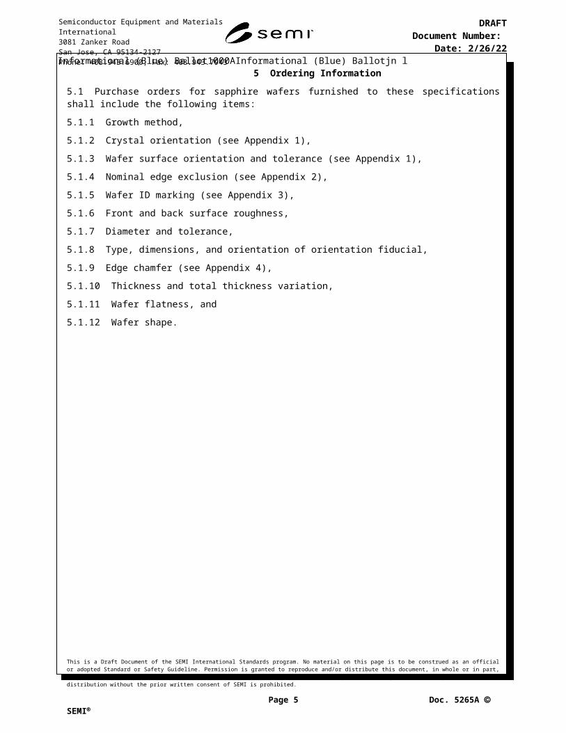
5 Ordering Information 5.1 Purchase orders for sapphire wafers furnished to these specifications shall include the following items:
5.1.1 Growth method,
5.1.2 Crystal orientation (see Appendix 1),
5.1.3 Wafer surface orientation and tolerance (see Appendix 1),
5.1.4 Nominal edge exclusion (see Appendix 2),
5.1.5 Wafer ID marking (see Appendix 3),
5.1.6 Front and back surface roughness,
5.1.7 Diameter and tolerance,
5.1.8 Type, dimensions, and orientation of orientation fiducial,
5.1.9 Edge chamfer (see Appendix 4),
5.1.10 Thickness and total thickness variation,
5.1.11 Wafer flatness, and
5.1.12 Wafer shape.
This is a Draft Document of the SEMI International Standards program. No material on this page is to be construed as an official or adopted Standard or Safety Guideline. Permission is granted to reproduce and/or distribute this document, in whole or in part, only within the scope of SEMI International Standards committee (document development) activity. All other reproduction and/or distribution without the prior written consent of SEMI is prohibited.
Page 3 Doc. jn l SEMI
Semiconductor Equipment and Materials International3081 Zanker RoadSan Jose, CA 95134-2127Phone: 408.943.6900, Fax: 408.943.7943

DRAFTDocument Number:
Date: 5/10/23
3: The traditional wafer shape terms “bow” and “warp” are measures of median surface variations. Because the main concern with the shape of sapphire wafers is the manner that they fit into epitaxial deposition equipment, the back surface variation is more significant than median surface variation. Therefore these terms have been modified to represent this fact. It should be possible to utilize the traditional values for these new parameters, but this remains to be established.
5.2 In addition, the purchase order must indicate the test method to be used in evaluating each of these items.
5.3 Also, bulk and front and back surface defects, such as bubbles, scratches, edge chips and indents, and surface contamination requirements together with appropriate test methodology should be included in the purchase order.
4: To be considered an edge chip the peripheral length and radial penetration must exceed a certain specified size.
5.4 The following items must also be included in the purchase order:
5.4.1 Sampling and lot acceptance procedures (see § 7),
5.4.2 Certification (if required) (see § 9) and
5.4.3 Packing and shipping container labeling requirements (see § 10).
5.5 Finally, several other characteristics may also be specified in purchase orders for sapphire wafers for any particular application. These can be selected from the items listed in the Sapphire Wafer Specification Format for Order Entry, Parts 1 and 2, which is given in Related Information 1 (see Table R1-1).
6 Requirements for Standardized Sapphire Wafers6.1 100 mm Sapphire Wafers for HB-LED Applications
6.1.1 One type of 100 mm diameter single-side polished c-axis sapphire wafers is commonly used in the high brightness LED (HB-LED) industry. Double-side polished wafers are also used, but these are not directly covered by this specification.
6.1.2 Standard specifications for this type of sapphire wafers are listed in Table 1.
5: Those necessary properties for which standardize values could not be agreed upon are listed “as specified in the purchase order or contract”. Values may be inserted when agreement in the industry is achieved. Meanwhile, see Related Information 1 for guidance in selecting such values.
6.1.3 If other types of wafers are required for an application or for research purposes, these may be ordered through the use of the sapphire wafer specification format for order entry, found in Table R1-1 in Related Information 1.
This is a Draft Document of the SEMI International Standards program. No material on this page is to be construed as an official or adopted Standard or Safety Guideline. Permission is granted to reproduce and/or distribute this document, in whole or in part, only within the scope of SEMI International Standards committee (document development) activity. All other reproduction and/or distribution without the prior written consent of SEMI is prohibited.
Page 4 Doc. jn l SEMI
Semiconductor Equipment and Materials International3081 Zanker RoadSan Jose, CA 95134-2127Phone: 408.943.6900, Fax: 408.943.7943
DRAFTDocument Number:
Date: 5/10/23
Table 1 Specifications for Flatted 100 mm Diameter, Polished Sapphire Wafers
Property Value
Wafer Category 4aThickness 650 ± 25 μmOrientation Fiducial FlatGrowth Method as specified in the purchase order or contractCrystal Orientation c-axis ±0.1ºWafer Surface Orientation Target as specified in the purchase order or contractWafer Surface Orientation Tolerance ±0.1ºNominal Edge Exclusion 2 mmWafer ID Marking on back surface as specified in purchase order or contractFront Surface polished, Ra ≤ 0.3 nmBack Surface fine ground, Ra = 1.0 ± 0.2 μmDiameter 100.0 ± 0.1 mmFlat Length 32.5 ± 1.0 mmFlat Misalignment a-plane ± 0.3ºEdge Chamfer as specified in the purchase order or contractTotal Thickness Variation (TTV) ≤20 mBack-surface Bow Target#1 as specified in the purchase order or contractBack-surface Bow Tolerance ±10 μmBack-surface Warp#2 ≤30 μmFlatness, SBIR as specified in the purchase order or contractScratches as specified in the purchase order or contractEdge Chips and Indents as specified in the purchase order or contractSurface Contamination as specified in the purchase order or contract
#1 Because it is sometimes desired to specify a slightly positive or negative value for bow, the target value is listed as “as specified in the pur-chase order or contract” and the deviation from this value is limited to 10 m larger or smaller, taking into account the sign of the bow.#2 Because warp can never be less than the magnitude of the bow of a wafer, no target value is specified. The maximum value of warp is given as 30 m and the minimum value can never be less than 0 m.
6.2 150 mm Sapphire Wafers for HB-LED Applications
6.2.1 Four types of 150 mm diameter single-side polished c-axis sapphire wafers are commonly used in the high brightness LED (HB-LED) industry. There are two thicknesses (1,000 and 1,300 m) and two types of fiducials (flat and notch).
6.3 Standard specifications for these four types of sapphire wafers are listed in Table 2.
6: Those necessary properties for which standardize values could not be agreed upon are listed “as specified in the purchase order or contract”. Values may be inserted when agreement in the industry is achieved. Meanwhile, see Related Information 1 for guidance in selecting such values.
6.4 If other types of wafers are required for an application or for research purposes, these may be ordered through the use of the sapphire wafer specification format for order entry, found in Table R1-1 in Related Information 1.
This is a Draft Document of the SEMI International Standards program. No material on this page is to be construed as an official or adopted Standard or Safety Guideline. Permission is granted to reproduce and/or distribute this document, in whole or in part, only within the scope of SEMI International Standards committee (document development) activity. All other reproduction and/or distribution without the prior written consent of SEMI is prohibited.
Page 5 Doc. jn l SEMI
Semiconductor Equipment and Materials International3081 Zanker RoadSan Jose, CA 95134-2127Phone: 408.943.6900, Fax: 408.943.7943
DRAFTDocument Number:
Date: 5/10/23
Table 2 Specifications for 150 mm Diameter, Polished c-Axis Sapphire Wafers
Property Value
Wafer Category 6a 6b 6c 6dThickness 1,000 μm 1,300 μm 1,000 μm 1,300 μmOrientation Fiducial Flat Flat Notch NotchGrowth Method as specified in the purchase order or contractCrystal Orientation c-axis ±0.1ºWafer Surface Orientation Target as specified in the purchase order or contractWafer Surface Orientation Tolerance ±0.1ºNominal Edge Exclusion 2 mmWafer ID Marking on back surface as specified in purchase order or contractFront Surface polished, Ra ≤ 0.3 nmBack Surface fine ground, Ra = 1.0 ± 0.2 μmDiameter 150.0 ± 0.2 mmFlat Length 47.5 ± 2.5 mm not applicableFlat Orientation a-plane ± 0.3º not applicableNotch Depth not applicable 1.00 mm +0.25 mm 0.00 mmNotch Angle not applicable 90 +5 1Orientation of Notch Axis not applicable a-axis ± 0.3ºEdge Chamfer (see Appendix 4) 200 ± 50 μmTotal Thickness Variation (TTV) ≤20 mBack-surface Bow Target#1 as specified in the purchase order or contractBack-surface Bow Tolerance ±10 μmBack-surface Warp#2 ≤30 μmFlatness, SBIR as specified in the purchase order or contractScratches as specified in the purchase order or contractEdge Chips and Indents as specified in the purchase order or contractSurface Contamination as specified in the purchase order or contract
#1 Because it is sometimes desired to specify a slightly positive or negative value for bow, the target value is listed as “as specified in the purchase order or contract” and the deviation from this value is limited to 10 m larger or smaller, taking into account the sign of the bow.
#2 Because warp can never be less than the magnitude of the bow of a wafer, no target value is specified. The maximum value of warp is given as 30 m and the minimum value can never be less than 0 m.
7 Sampling7.1 Unless otherwise specified, ASTM Practice E122 shall be used. When so specified, appropriate sample size shall be selected from each lot in accordance with ANSI/ASQC Z1.4. Each quality characteristic shall be assigned an acceptable quality level (AQL) and lot total percent defective (LTPD) value in accordance with ANSI/ASQC Z1.4-1993 definitions for critical, major, and minor classifications. If desired and so specified in the contract or order, each of these classifications may alternatively be assigned cumulative AQL and LTPD values. Inspection levels shall be agreed upon between the supplier and the customer.
8 Test Methods8.1 Measurements shall be made or certifiable to one of the SEMI or JIS standard test methods for the item as selected from Table R1-1 and specified in the purchase order (see also Related Information 2).
8.2 If several different standard test methods for an item are commonly used within a region, it is particularly important that the applicable method of test be identified in the purchase order.
This is a Draft Document of the SEMI International Standards program. No material on this page is to be construed as an official or adopted Standard or Safety Guideline. Permission is granted to reproduce and/or distribute this document, in whole or in part, only within the scope of SEMI International Standards committee (document development) activity. All other reproduction and/or distribution without the prior written consent of SEMI is prohibited.
Page 6 Doc. jn l SEMI
Semiconductor Equipment and Materials International3081 Zanker RoadSan Jose, CA 95134-2127Phone: 408.943.6900, Fax: 408.943.7943

DRAFTDocument Number:
Date: 5/10/23
8.3 If no method of test is specified in the purchase order and if standard test methods from different geographic regions are available, the default method shall be a method in common usage for the region of the purchaser of the wafer.
8.4 If no standard test method for an item is available, the test procedure to be used must be agreed upon between supplier and customer.
9 Certification9.1 Upon request of the customer in the contract or order, a manufacturer’s or supplier’s certification that the material was manufactured and tested in accordance with this specification, together with a report of the test results, shall be furnished at the time of shipment.
9.2 In the interest of controlling inspection costs, the supplier and the customer may agree that the material shall be certified as “capable of meeting” certain requirements. In this context, “capable of meeting” shall signify that the supplier is not required to perform the appropriate tests listed in Table R1-1, Part 2. However, if the customer performs the test and the material fails to meet the requirement, the material may be subject to rejection.
10 Packing and Marking10.1 Special packing requirements shall be subject to agreement between the supplier and the customer. Otherwise all wafers shall be handled, inspected, and packed in such a manner as to avoid chipping, scratches, and contamination, and in accordance with the best industry practices to provide ample protection against damage during shipment.
10.2 The substrates supplied under these specifications shall be identified by appropriately labeling the outside of each box or other container, and each subdivision thereof, in which it may reasonably be expected that the substrates will be stored prior to further processing. Identification shall include, as minimum, the nominal diameter, orientation, and lot number. The lot number, either (1) assigned by original manufacturer of the substrates, or (2) assigned subsequent to substrate’s manufacture, but providing reference to the original lot number, shall provide ready access to information concerning the fabrication history of the particular substrates in that lot. Such information shall be retained on file at the manufacturer’s facility for at least one year after the customer has accepted particular lot.
This is a Draft Document of the SEMI International Standards program. No material on this page is to be construed as an official or adopted Standard or Safety Guideline. Permission is granted to reproduce and/or distribute this document, in whole or in part, only within the scope of SEMI International Standards committee (document development) activity. All other reproduction and/or distribution without the prior written consent of SEMI is prohibited.
Page 7 Doc. jn l SEMI
Semiconductor Equipment and Materials International3081 Zanker RoadSan Jose, CA 95134-2127Phone: 408.943.6900, Fax: 408.943.7943

DRAFTDocument Number:
Date: 5/10/23
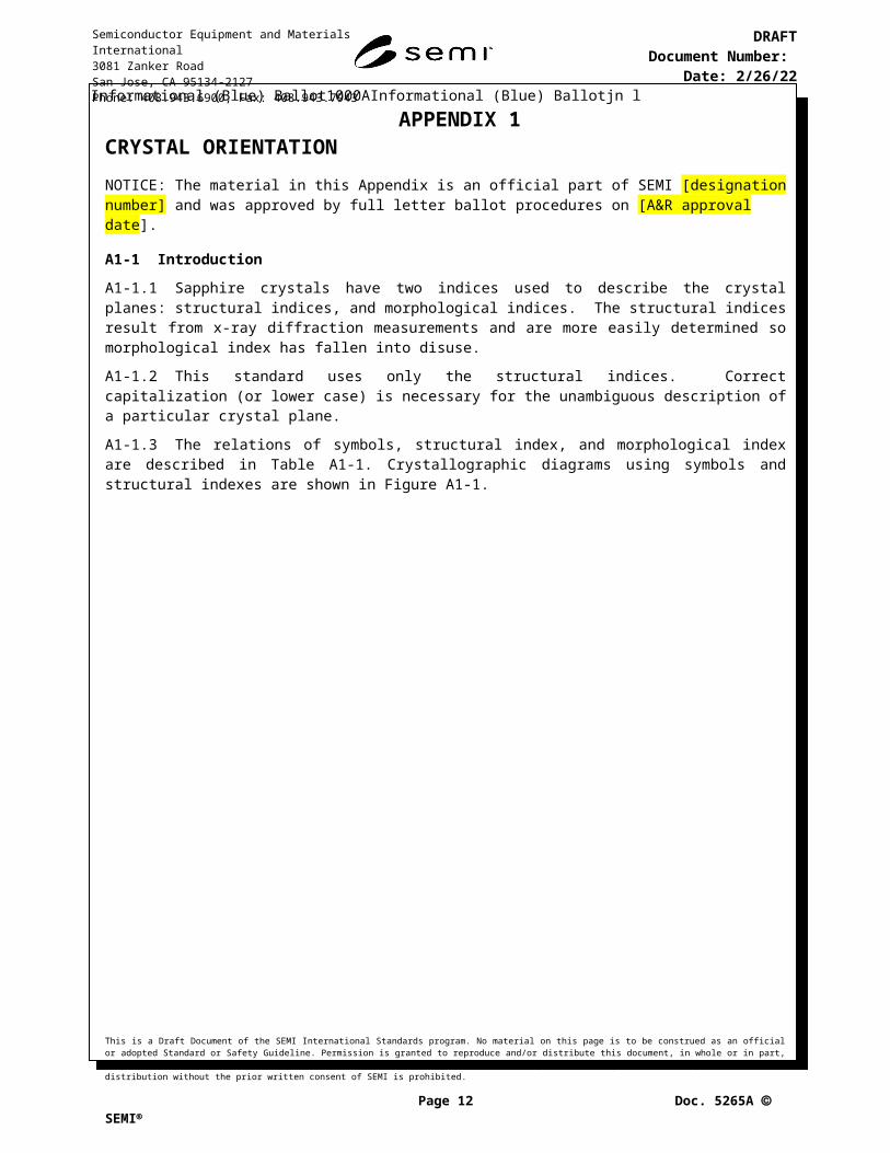
APPENDIX 1CRYSTAL ORIENTATIONNOTICE: The material in this Appendix is an official part of SEMI [designation number] and was approved by full letter ballot procedures on [A&R approval date].
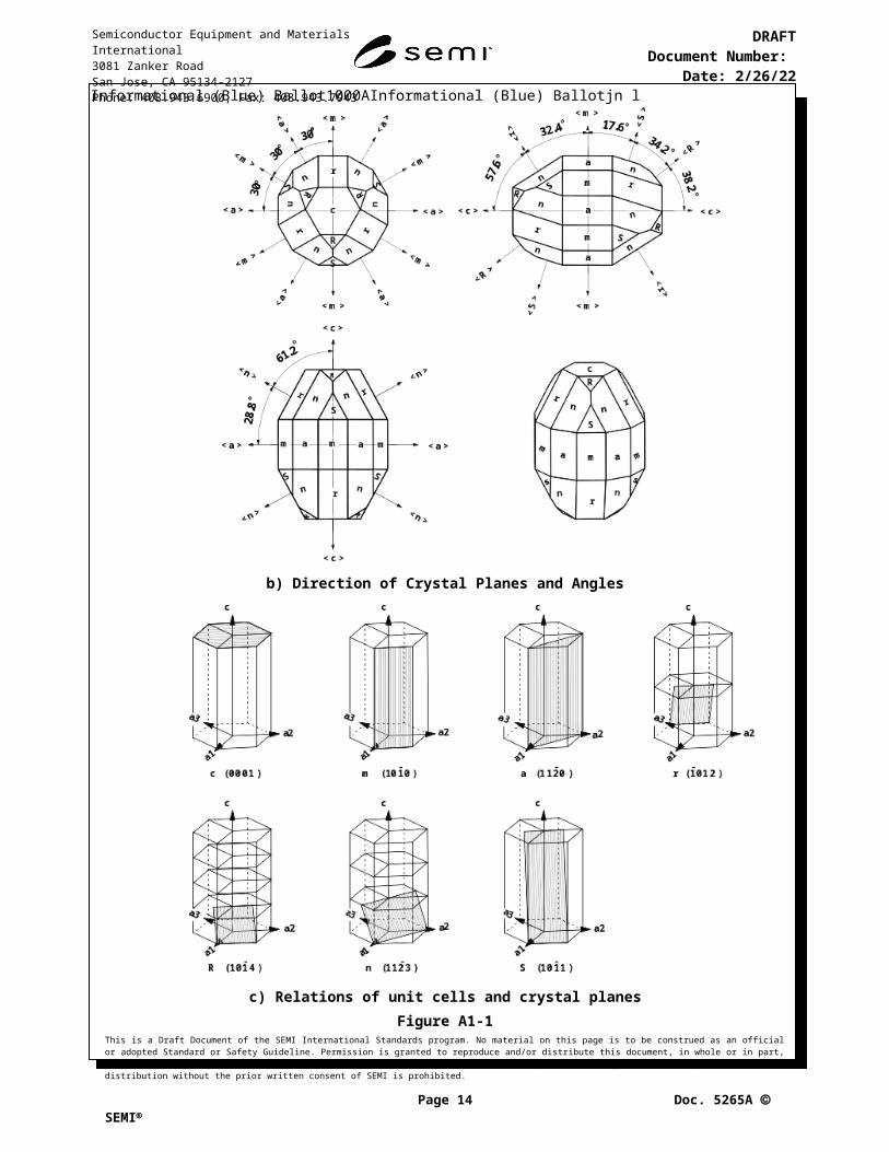
A1-1 IntroductionA1-1.1 Sapphire crystals have two indices used to describe the crystal planes: structural indices, and morphological indices. The structural indices result from x-ray diffraction measurements and are more easily determined so morphological index has fallen into disuse.
A1-1.2 This standard uses only the structural indices. Correct capitalization (or lower case) is necessary for the unambiguous description of a particular crystal plane.
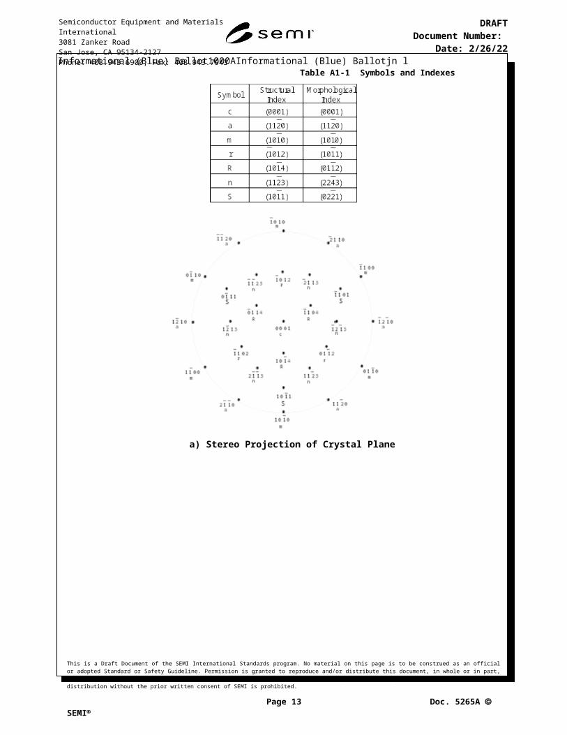
A1-1.3 The relations of symbols, structural index, and morphological index are described in Table A1-1. Crystallographic diagrams using symbols and structural indexes are shown in Figure A1-1.
Table A1-1 Symbols and Indexes
a) Stereo Projection of Crystal Plane
This is a Draft Document of the SEMI International Standards program. No material on this page is to be construed as an official or adopted Standard or Safety Guideline. Permission is granted to reproduce and/or distribute this document, in whole or in part, only within the scope of SEMI International Standards committee (document development) activity. All other reproduction and/or distribution without the prior written consent of SEMI is prohibited.
Page 8 Doc. jn l SEMI
Semiconductor Equipment and Materials International3081 Zanker RoadSan Jose, CA 95134-2127Phone: 408.943.6900, Fax: 408.943.7943
DRAFTDocument Number:
Date: 5/10/23
b) Direction of Crystal Planes and Angles
c) Relations of unit cells and crystal planesFigure A1-1
Crystallographic Diagrams of Sapphire
This is a Draft Document of the SEMI International Standards program. No material on this page is to be construed as an official or adopted Standard or Safety Guideline. Permission is granted to reproduce and/or distribute this document, in whole or in part, only within the scope of SEMI International Standards committee (document development) activity. All other reproduction and/or distribution without the prior written consent of SEMI is prohibited.
Page 9 Doc. jn l SEMI
Semiconductor Equipment and Materials International3081 Zanker RoadSan Jose, CA 95134-2127Phone: 408.943.6900, Fax: 408.943.7943

DRAFTDocument Number:
Date: 5/10/23
APPENDIX 2NOMINAL EDGE EXCLUSION AND FIXED QUALITY AREANOTICE: The material in this Appendix is an official part of SEMI [designation number] and was approved by full letter ballot procedures on [A&R approval date].
A2-1 IntroductionA2-1.1 The nominal edge exclusion, EE, specifies the diameter of the fixed quality area (FQA), which is given by the nominal diameter minus 2·EE (see Figure A2-1). The fixed quality area is a center-referenced region that is independent in size from the tolerances of wafer diameter and, for flatted wafers, flat length. For the purposes of defining the FQA, the periphery of a wafer of nominal dimensions at a location with a notch is assumed to follow the circumference of a circle with diameter equal to the nominal wafer diameter.
A2-1.2 The nominal edge exclusion is usually specified as 2 mm. However, it should be noted that not all processes and metrology can work as close to the wafer edge as implied by the nominal edge exclusion.
A2-1.3 Figure A2-1a shows the nominal wafer diameter, the nominal edge exclusion, and the fixed quality area for a flatted wafer. Note that the boundary of the fixed quality area follows the flat a distance equal to the nominal edge exclusion toward the center of the wafer.
A2-1.4 Figure A2-1b shows the nominal wafer diameter, the nominal edge exclusion, and the fixed quality area for a notched wafer. Note that the boundary of the fixed quality area is circular around the entire periphery of the wafer, ignoring the presence of the notch.
A2-1.5 Figure A2-1c is an expanded region of a portion of the wafer periphery showing the nominal wafer periphery, the wafer periphery limits of actual wafers, and the flatness quality area boundary.
A2-1.6 In addition, it is sometimes necessary to specify additional exclusion zones, such as those for wafer identification marks or wafer holding areas.
A2-1.7 Although use of edge-referenced properties is discouraged, some equipment and procedures are based on edge-referenced dimensions. When this occurs, the quality area is not fixed and some part of the fixed quality area may fall outside the evaluated area, which is generally not a desirable situation.
This is a Draft Document of the SEMI International Standards program. No material on this page is to be construed as an official or adopted Standard or Safety Guideline. Permission is granted to reproduce and/or distribute this document, in whole or in part, only within the scope of SEMI International Standards committee (document development) activity. All other reproduction and/or distribution without the prior written consent of SEMI is prohibited.
Page 10 Doc. jn l SEMI
Semiconductor Equipment and Materials International3081 Zanker RoadSan Jose, CA 95134-2127Phone: 408.943.6900, Fax: 408.943.7943

DRAFTDocument Number:
Date: 5/10/23
F ix e d Q u a l i t y A r e a
E E = N o m i n a l E d g e E x c l u s i o n
F Q A B o u n d a r y
N o m i n a l W a f e r P e r i p h e r yP r i m a r y F l a t
Second
ary F
lat
F ix e d Q u a l i t y A r e a
E E = N o m i n a l E d g e E x c l u s i o nE E = N o m i n a l E d g e E x c l u s i o n
F Q A B o u n d a r yF Q A B o u n d a r y
N o m i n a l W a f e r P e r i p h e r yN o m i n a l W a f e r P e r i p h e r yP r i m a r y F l a t
Second
ary F
lat
N o t c hN o m i n a l W a f e r P e r i p h e r y
F Q A B o u n d a r y
E E = N o m i n a l E d g e E x c l u s i o n
F i x e d Q u a l i t y A r e a
N o t c hN o t c hN o m i n a l W a f e r P e r i p h e r yN o m i n a l W a f e r P e r i p h e r y
F Q A B o u n d a r yF Q A B o u n d a r y
E E = N o m i n a l E d g e E x c l u s i o nE E = N o m i n a l E d g e E x c l u s i o n
F i x e d Q u a l i t y A r e aF i x e d Q u a l i t y A r e a
E E = N o m i n a l E d g e E x c l u s i o n
A c t u a l W a f e r P e r i p h e r y L im i t s F Q A B o u n d a r y
N o m i n a l W a f e r P e r i p h e r y
F i x e d Q u a l i t y A r e a E E = N o m i n a l E d g e E x c l u s i o n E E = N o m i n a l E d g e E x c l u s i o n
A c t u a l W a f e r P e r i p h e r y L im i t s A c t u a l W a f e r P e r i p h e r y L im i t s F Q A B o u n d a r y F Q A B o u n d a r y
N o m i n a l W a f e r P e r i p h e r y N o m i n a l W a f e r P e r i p h e r y
F i x e d Q u a l i t y A r e a
c . N o m i n a l a n d A c t u a l W a f e r P e r i p h e r i e s
b . N o t c h e d W a f e r
a . F l a t t e d W a f e r
E E = N o m i n a l E d g e E x c l u s i o n
F l a t
F i x e d Q u a l i t y A r e a
N o m i n a l W a f e r P e r i p h e r y
F Q A B o u n d a r y
Figure A2-1Fixed Quality Area
This is a Draft Document of the SEMI International Standards program. No material on this page is to be construed as an official or adopted Standard or Safety Guideline. Permission is granted to reproduce and/or distribute this document, in whole or in part, only within the scope of SEMI International Standards committee (document development) activity. All other reproduction and/or distribution without the prior written consent of SEMI is prohibited.
Page 11 Doc. jn l SEMI
Semiconductor Equipment and Materials International3081 Zanker RoadSan Jose, CA 95134-2127Phone: 408.943.6900, Fax: 408.943.7943

DRAFTDocument Number:
Date: 5/10/23
APPENDIX 3WAFER MARKS ON 100 AND 150 mm SAPPHIRE WAFERSNOTICE: The material in this Appendix is an official part of SEMI [designation number] and was approved by full letter ballot procedures on [A&R approval date].
A3-1 Message Content of Wafer Mark SymbolsA3-1.1 Each wafer mark symbol shall contain 10 message characters. Alphanumeric symbols shall also contain the two check characters of the alphanumeric error detecting method described in SEMI M12, which should be consulted for the details.
A3-1.2 Other mark symbols may also be employed as specified in the purchase order or contract. Such other symbols may have different error identification and correction methods.
A3-1.3 The message characters may include the following: A–Z, 0–9, and dash (–). These characters are included in the SEMI OCR Character Set, which also includes a period (.) that is not used in here. This is the same character set specified in SEMI M12. It is reproduced in Figure A3-1, and the outlines are given in SEMI AUX 015.4 The ten message characters shall contain two elements:
1. a vendor-assigned 8-character wafer identification code, followed by
2. a 2-character vendor identification code.
Figure A3-1SEMI OCR Character Set as Modified for this Application
A3-2 Locations of the ID Marks A3-2.1 All ID marks shall be placed on the back surface of the wafer on the side of the wafer near the fiducial.
7: Until appropriate experiments are completed the nature of the markings, the type of markings (other than alphanumeric), and the exact locations on the wafer cannot be specified. It is expected that such experiments will be completed soon after the end of 2012 at which time this appendix will be appropriately expanded.
4 SEMI OCR Character Outlines.
This is a Draft Document of the SEMI International Standards program. No material on this page is to be construed as an official or adopted Standard or Safety Guideline. Permission is granted to reproduce and/or distribute this document, in whole or in part, only within the scope of SEMI International Standards committee (document development) activity. All other reproduction and/or distribution without the prior written consent of SEMI is prohibited.
Page 12 Doc. jn l SEMI
Semiconductor Equipment and Materials International3081 Zanker RoadSan Jose, CA 95134-2127Phone: 408.943.6900, Fax: 408.943.7943
DRAFTDocument Number:
Date: 5/10/23
APPENDIX 4EDGE CHAMFERNOTICE: The material in this Appendix is an official part of SEMI [designation number] and was approved by full letter ballot procedures on [A&R approval date].
A4-1 IntroductionA4-1.1 The edge chamfer shall be 200 ± 50 m so that the edge of the wafer fits within the template shown in Figure A4-1 and Table A4-1, unless otherwise stated in the purchase order or contract.
Figure A4-1Sapphire Edge Template Showing Edge Chamfer
Table A4-2 Sapphire Wafer Taper Template Coordinates
Point x-coordinate y-coordinate
A 150 m 0 mB 250 m 0 mC 0 m 250 mD 0 m 150 m
This is a Draft Document of the SEMI International Standards program. No material on this page is to be construed as an official or adopted Standard or Safety Guideline. Permission is granted to reproduce and/or distribute this document, in whole or in part, only within the scope of SEMI International Standards committee (document development) activity. All other reproduction and/or distribution without the prior written consent of SEMI is prohibited.
Page 13 Doc. jn l SEMI
D
C
B
y-axis
x-axis Wafer front or back surfaceA
Wafer median plane
Semiconductor Equipment and Materials International3081 Zanker RoadSan Jose, CA 95134-2127Phone: 408.943.6900, Fax: 408.943.7943
DRAFTDocument Number:
Date: 5/10/23
RELATED INFORMATION 1 SAPPHIRE WAFER SPECIFICATION FORMAT FOR ORDER ENTRYNOTICE: This related information is not an official part of SEMI [designation number]. It was derived during the course of development of this standard. This related information was approved for publication by full letter ballot.
R1-1 IntroductionR1-1.1 For those properties for which standardized values have been agreed upon for the five standardized categories of sapphire wafers, the first column of the specification format for order entry in Table R1-1 contains the following symbol: .
R1-1.2 For those properties that have not yet had agreed upon standardized values, the format for order entry provides guidance as to appropriate values. At this stage, however, any value can be specified so long as supplier and customer agree that it can be manufactured.
R1-1.3 In addition, standardized sapphire wafers may not be suitable for all applications in the HB-LED industry. To facilitate the purchase of other types of sapphire
Table R1-1 Sapphire Wafer Specification Format for Order Entry, Parts 1 and 2Part 1 General Information
ITEM INFORMATION Date:
Customer NamePurchase Order NumberLine NumberItem NumberGeneral Specification NumberRevision LevelPart Number/Revision
Part 2 Polished Wafer or Substrate
ITEM SPECIFICATION MEASUREMENT METHOD
2-1 GENERAL CHARACTERISTICS2-1.1 Growth Process as specified in purchase order or contract
2-1.2 Crystal Orientation [ ] c-axis; [ ] Other (specify) __________ [ ] SEMI MF26 (X-Ray); [ ] SEMI MF26 (Optical); [ ] Other: (specify)____________
2-1.3.1 Wafer Surface Orientation Target
[ ] On-axis (c): 0.00º ± 0.1ºOff-orientation: [ ] c Misorientation to m: ____º ± 0.1º; [ ] c Misorientation to a: ____º ± 0.1º
[ ] SEMI MF26 (X-Ray); [ ] SEMI MF26 (Optical); [ ] Other: (specify)____________
2-1.3.2 Wafer Surface Orientation Tolerance
[ ] ±0.1º; [ ] Other: (specify)_______º [ ] As agreed between supplier and customer
2-1.6 Edge Exclusion [ ] 1 mm; [ ] 2 mm; [ ] Other: (specify)______mm [ ] As agreed between supplier and customer
2-2 WAFER PREPARATION CHARACTERISTICS2-2.1 Wafer ID Marking [ ] None; [ ] Alphanumeric;
[ ] Other: (specify) _______ 2-2.2 Front Surface Condition [ ] Polished (Ra≤ 0.3 nm); [ ] Other Ra ≤ _____nm [ ] As agreed between supplier and
customer 2-2.3 Back Surface Condition [ ] Fine Ground (Ra = 1.0 ± 0.2 m);
[ ] Other: Ra = _____ ± _______ μm[ ] As agreed between supplier and customer
2-3 DIMENSIONAL CHARACTERISTICS
This is a Draft Document of the SEMI International Standards program. No material on this page is to be construed as an official or adopted Standard or Safety Guideline. Permission is granted to reproduce and/or distribute this document, in whole or in part, only within the scope of SEMI International Standards committee (document development) activity. All other reproduction and/or distribution without the prior written consent of SEMI is prohibited.
Page 14 Doc. jn l SEMI
Semiconductor Equipment and Materials International3081 Zanker RoadSan Jose, CA 95134-2127Phone: 408.943.6900, Fax: 408.943.7943
DRAFTDocument Number:
Date: 5/10/23
ITEM SPECIFICATION MEASUREMENT METHOD 2-3.1 Diameter [ ] 100 ± 0.1 mm; [ ] 100 ± 0.4 mm;
[ ] 100 ± 0.5 mm; [ ] 100 ± ______ mm; [ ] 150 ± 0.2 mm; [ ] 150 ± 0.1 mm; [ ] 150 ± 0.25 mm; [ ] 150 ± ______ mm;
[ ] SEMI MF2074; [ ] Other: (specify)___________
2-3.2 Orientation Fiducial [ ] Flat; [ ] Notch 2-3.3 Fiducial Dimensions Flat Length [ ] 32.5 ±1.0 mm; [ ] 32.5 ± 2.0 mm;
[ ] 47.5 ± 2.5 mm; [ ] 45.0 ± 1.0 mm; [ ] Other: (specify)_______ ±________ mm Notch Depth [ ] 1.00 mm +0.25 mm 0.00 mm Notch Angle [ ] 90° +5° 1°
[ ] SEMI MF671 (Flat Length); [ ] SEMI MF1152 (Notch Dimensions); [ ] Other: (specify)___________
2-3.4 Fiducial Orientation[ ] a-plane (112 0)± __º; [ ] m-plane (1010 )± __º
[ ] As agreed between supplier and customer; [ ] SEMI MF847 (for flat only); [ ] Other: (specify)___________
#1 2-3.5 Edge Chamfer (see Figure A4-1)
[ ] 200 ± 50 μm; [ ] Other (specify)______ ±_______m
SEMI MF928: Method A [ ], Method B [ ]; [ ] Other: (specify)___________
2-3.6 Thickness 100 mm dia
150 mm dia
[ ] 650 ± 25 μm; [ ] 650 ± 15 μm;[ ] Other (specify) _______±_________ [ ] 1000 ± 25 µm; [ ] 1300 ± 25 μm; [ ] Other (specify) _______±_________
[ ] SEMI MF533; [ ] SEMI MF1530; [ ] JIS H 0611; [ ] Other: (specify)___________
2-3.7 Total Thickness Variation (TTV)
[ ] ≤10 µm; [ ] ≤20 μm; [ ] ≤25 μm; [ ] ≤50 μm; [ ] Other (specify) ≤ ____ μm
[ ] SEMI MF533 (5-point pattern); [ ] SEMI MF533 (5-point pattern); [ ] JIS H 0611; [ ] SEMI MF657 (partial scan); [ ] SEMI MF1530 (full scan); [ ] Other: (specify)___________
2-3.8 Back-surface Bow Target
[ ] Specify:_____m [ ] As agreed between supplier and customer;
2-3.9 Back-surface Bow Tolerance
[ ] ±10 m; [ ] ±15 µm [ ] Other (specify): ±_____m
[ ] As agreed between supplier and customer;
2-3.10 Back-surface Warp [ ] 30 µm, max; [ ] Other (specify) _____m, max [ ] As agreed between supplier and customer;
2-3.11 Flatness, SBIR [ ] ≤1 μm; [ ] ≤5 μm; [ ] Other __m Site Size ___ mm × ___ mm [ ]% Usable Area________ [ ] Include; [ ] Do not include partial sites Offset: x = [ ] mm, y = [ ] mm
[ ] SEMI MF1530; [ ] Other: (specify)___________
2-4 FRONT SURFACE INSPECTION CHARACTERISTICS2-4.1 Scratches [ ] Number ≤________; [ ] Length ____________;
[ ] Depth __________; [ ] Width ___________[ ] SEMI MF523; [ ] JIS H 0614; [ ] Other: (specify)___________
2-4.2 Edge Chips and Indents (See Note 4)
[ ] Number ≤ ___; [ ] Peripheral Length ≥ ___ μm; [ ] Radial Penetration ≥ _______μm
[ ] SEMI MF523; [ ] JIS H 0614; [ ] Other: (specify)___________
2-4.3 Surface Contamination [ ] ≤____ Particles / Wafer [ ] Particle Size ≤____ μm; [ ] Other _______
[ ] SEMI MF523; [ ] JIS H 0614; [ ] Other: (specify)___________
2-5 BACK SURFACE INSPECTION CHARACTERISTICS2-5.1 Scratches [ ] Number _________; [ ] Length ____________;
[ ] Depth ___________; Width ___________[ ] SEMI MF523; [ ] JIS H 0614; [ ] Other: (specify)___________
2-5.2 Edge Chips and Indents (See Note 4)
[ ] Number ≤ ___; [ ] Peripheral Length ≥ ___ μm; [ ] Radial Penetration ≥ _______μm
[ ] SEMI MF523; [ ] JIS H 0614; [ ] Other: (specify)___________
#1 The edge chamfer dimensions are standardized only for category 6a, 6b, 6c, and 6d wafers.
This is a Draft Document of the SEMI International Standards program. No material on this page is to be construed as an official or adopted Standard or Safety Guideline. Permission is granted to reproduce and/or distribute this document, in whole or in part, only within the scope of SEMI International Standards committee (document development) activity. All other reproduction and/or distribution without the prior written consent of SEMI is prohibited.
Page 15 Doc. jn l SEMI
Semiconductor Equipment and Materials International3081 Zanker RoadSan Jose, CA 95134-2127Phone: 408.943.6900, Fax: 408.943.7943
DRAFTDocument Number:
Date: 5/10/23
RELATED INFORMATION 2 TEST METHODSNOTICE: This related information is not an official part of SEMI [designation number]. It was derived during the course of development of this standard. This related information was approved for publication by full letter ballot.
R2-1 IntroductionR2-1.1 Information about the various test methods listed in Table R1-1 is provided in this Related Information section together with information about some additional test methods no longer in wide use throughout the industry. Where no test method is specified in table R1-1, the method to be used should be agreed upon between supplier and customer.
8: The following test methods are suggested, but supplier and customer can, if they wish, agree on other acceptable test methods.
9: Sapphire substrates are highly susceptible to surface damage. While the mechanical dimensions of a wafer can be measured by use of tools such as micrometer calipers and other conventional techniques, the substrate may be damaged physically in ways that are not immediately evident. Special attentions must therefore be paid in the selection and execution of measurement methods.
R2-2 General CharacteristicsR2-2.1 Growth Method — No standardized test method. Should be reported by supplier.
R2-2.2 Crystal and Wafer Surface Orientation — Determine using the x-ray method of SEMI MF26. Some modification of the calculations in this test method may be required.
R2-2.3 Edge Exclusion — No standardized test method.
R2-3 Wafer Preparation CharacteristicsR2-3.1 Wafer ID Marking — No standardized test method.
R2-3.2 Front and Back Surface Roughness — No standardized test method.
R2-4 DimensionsR2-4.1 Diameter — Determine by a method agreed upon between the supplier and the customer at locations specified in Configuration 1 of SEMI MF2074.
R2-4.2 Fiducial Dimensions — Unless otherwise specified, determine flat length in accordance with SEMI MF671, and determine the notch dimensions in accordance with SEMI MF1152.
R2-4.3 Fiducial Orientation — Determine in accordance with a method agreed upon between supplier and customer. SEMI MF847 should be suitable for measuring the orientation of a flat, but there is no standardized method for determining the orientation of a notch.
R2-4.4 Edge Chamfer— Determine by methods agreed upon between the supplier and the customer. Method B of SEMI MF928 is a non-destructive way of evaluating the shape of the edge profile (see Figure R4-1 and Table R4-1 for the shape and dimensions of an appropriate template.
R2-4.5 Thickness, Center Point — Unless otherwise specified, determine at the center of the wafer (Point 2 in Figure 5) in accordance with SEMI MF533.
R2-4.6 Total Thickness Variation — Unless otherwise specified, determine in accordance with SEMI MF533 using a five point or nine-point pattern as specified (see Note 10). Alternatively, determine over a partial scan using SEMI MF657 or over a full scan using SEMI MF1530.
10: The 5-point pattern of MF533 is widely used for flatted wafers and the 9-point pattern of MF533 is widely used for notched wafers.
R2-4.7 Back-surface Bow — Determine by methods agreed upon between the supplier and the customer. A mutually agreed upon modification of SEMI MF534 may be suitable.
R2-4.8 Back-surface Warp — Determine by methods agreed upon between the supplier and the customer. A mutually agreed upon modification of SEMI MF657 may be suitable.
This is a Draft Document of the SEMI International Standards program. No material on this page is to be construed as an official or adopted Standard or Safety Guideline. Permission is granted to reproduce and/or distribute this document, in whole or in part, only within the scope of SEMI International Standards committee (document development) activity. All other reproduction and/or distribution without the prior written consent of SEMI is prohibited.
Page 16 Doc. jn l SEMI
Semiconductor Equipment and Materials International3081 Zanker RoadSan Jose, CA 95134-2127Phone: 408.943.6900, Fax: 408.943.7943
DRAFTDocument Number:
Date: 5/10/23
R2-4.9 Flatness(SBIR) — Unless otherwise specified, determine in accordance with SEMI MF1530.
R2-5 Front and Back Surface Inspection CharacteristicsR2-5.1 Scratches — Unless otherwise specified, determine in accordance with SEMI MF523.
R2-5.2 Edge Chips and Indents — Unless otherwise specified, determine defects in accordance with SEMI MF523 (see Note 4).
R2-5.3 Surface Contamination — Unless otherwise specified, determine defects in accordance with SEMI MF523.
NOTICE: Semiconductor Equipment and Materials International (SEMI) makes no warranties or representations as to the suitability of the Standards and Safety Guidelines set forth herein for any particular application. The determination of the suitability of the Standard or Safety Guideline is solely the responsibility of the user. Users are cautioned to refer to manufacturer’s instructions, product labels, product data sheets, and other relevant literature, respecting any materials or equipment mentioned herein. Standards and Safety Guidelines are subject to change without notice.
By publication of this Standard or Safety Guideline, SEMI takes no position respecting the validity of any patent rights or copyrights asserted in connection with any items mentioned in this Standard or Safety Guideline. Users of this Standard or Safety Guideline are expressly advised that determination of any such patent rights or copyrights, and the risk of infringement of such rights are entirely their own responsibility.
This is a Draft Document of the SEMI International Standards program. No material on this page is to be construed as an official or adopted Standard or Safety Guideline. Permission is granted to reproduce and/or distribute this document, in whole or in part, only within the scope of SEMI International Standards committee (document development) activity. All other reproduction and/or distribution without the prior written consent of SEMI is prohibited.
Page 17 Doc. jn l SEMI
Semiconductor Equipment and Materials International3081 Zanker RoadSan Jose, CA 95134-2127Phone: 408.943.6900, Fax: 408.943.7943