Embed Size (px)
Citation preview
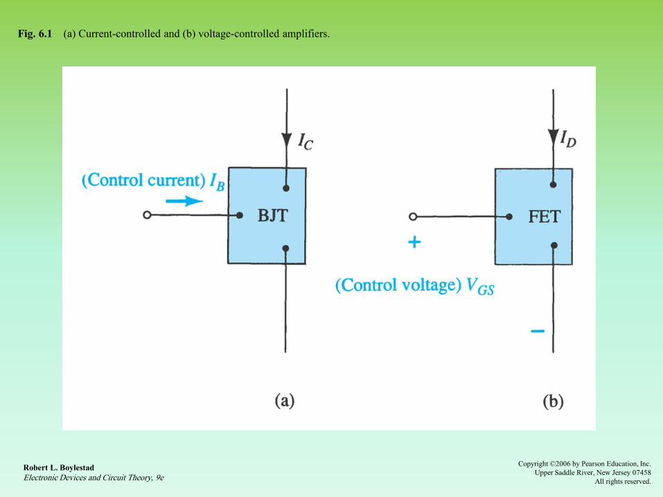
Fig. 6.1 (a) Current-controlled and (b) voltage-controlled amplifiers.
Robert L. Boylestad
Electronic Devices and Circuit Theory, 9e
Copyright ©2006 by Pearson Education, Inc.
Upper Saddle River, New Jersey 07458
All rights reserved.

Fig. 6.2 Drs. Ian Munro Ross (front) and G. C. Dacey jointly developed an experimental procedure for measuring the
characteristics of a field-effect transistor in 1955. (Photo Courtesy of AT&T Archives).
Robert L. Boylestad
Electronic Devices and Circuit Theory, 9e
Copyright ©2006 by Pearson Education, Inc.
Upper Saddle River, New Jersey 07458
All rights reserved.
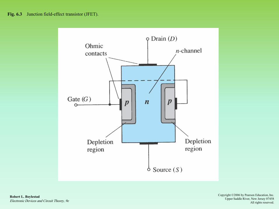
Fig. 6.3 Junction field-effect transistor (JFET).
Robert L. Boylestad
Electronic Devices and Circuit Theory, 9e
Copyright ©2006 by Pearson Education, Inc.
Upper Saddle River, New Jersey 07458
All rights reserved.

Fig. 6.4 Water analogy for the JFET control mechanism.
Robert L. Boylestad
Electronic Devices and Circuit Theory, 9e
Copyright ©2006 by Pearson Education, Inc.
Upper Saddle River, New Jersey 07458
All rights reserved.

Fig. 6.5 JFET at VGS = 0 V and VDS > 0 V.
Robert L. Boylestad
Electronic Devices and Circuit Theory, 9e
Copyright ©2006 by Pearson Education, Inc.
Upper Saddle River, New Jersey 07458
All rights reserved.

Fig. 6.6 Varying reverse-bias potentials across the p–n junction of an n-channel JFET.
Robert L. Boylestad
Electronic Devices and Circuit Theory, 9e
Copyright ©2006 by Pearson Education, Inc.
Upper Saddle River, New Jersey 07458
All rights reserved.

Fig. 6.7 ID versus VDS for VGS = 0 V.
Robert L. Boylestad
Electronic Devices and Circuit Theory, 9e
Copyright ©2006 by Pearson Education, Inc.
Upper Saddle River, New Jersey 07458
All rights reserved.

Fig. 6.8 Pinch-off (VGS = 0 V, VDS = VP).
Robert L. Boylestad
Electronic Devices and Circuit Theory, 9e
Copyright ©2006 by Pearson Education, Inc.
Upper Saddle River, New Jersey 07458
All rights reserved.

Fig. 6.9 Current source equivalent for VGS = 0 V, VDS > VP.
Robert L. Boylestad
Electronic Devices and Circuit Theory, 9e
Copyright ©2006 by Pearson Education, Inc.
Upper Saddle River, New Jersey 07458
All rights reserved.

Fig. 6.10 Application of a negative voltage to the gate of a JFET.
Robert L. Boylestad
Electronic Devices and Circuit Theory, 9e
Copyright ©2006 by Pearson Education, Inc.
Upper Saddle River, New Jersey 07458
All rights reserved.

Fig. 6.11 n-Channel JFET characteristics with IDSS = 8 mA and VP = -4 V.
Robert L. Boylestad
Electronic Devices and Circuit Theory, 9e
Copyright ©2006 by Pearson Education, Inc.
Upper Saddle River, New Jersey 07458
All rights reserved.

Fig. 6.12 p-Channel JFET.
Robert L. Boylestad
Electronic Devices and Circuit Theory, 9e
Copyright ©2006 by Pearson Education, Inc.
Upper Saddle River, New Jersey 07458
All rights reserved.
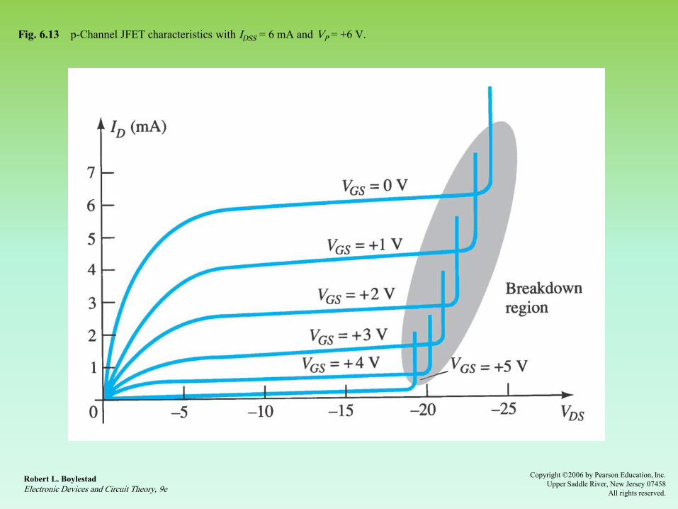
Fig. 6.13 p-Channel JFET characteristics with IDSS = 6 mA and VP = +6 V.
Robert L. Boylestad
Electronic Devices and Circuit Theory, 9e
Copyright ©2006 by Pearson Education, Inc.
Upper Saddle River, New Jersey 07458
All rights reserved.
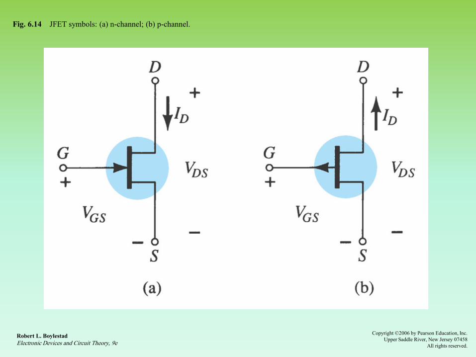
Fig. 6.14 JFET symbols: (a) n-channel; (b) p-channel.
Robert L. Boylestad
Electronic Devices and Circuit Theory, 9e
Copyright ©2006 by Pearson Education, Inc.
Upper Saddle River, New Jersey 07458
All rights reserved.

Fig. 6.15 (a) VGS = 0 V, ID = IDSS; (b) cutoff (ID = 0 A) VGS less than the pinch-off level; (c) ID is between 0 A and IDSS
for VGS ≤ 0 V and greater than the pinch-off level.
Robert L. Boylestad
Electronic Devices and Circuit Theory, 9e
Copyright ©2006 by Pearson Education, Inc.
Upper Saddle River, New Jersey 07458
All rights reserved.
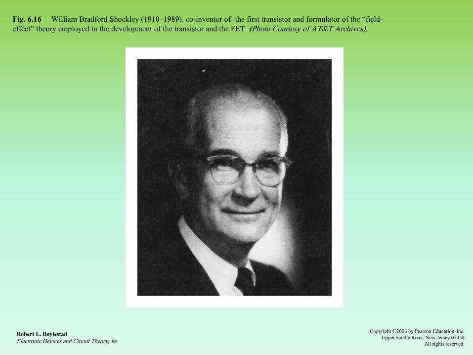
Fig. 6.16 William Bradford Shockley (1910–1989), co-inventor of the first transistor and formulator of the “field-
effect” theory employed in the development of the transistor and the FET. (Photo Courtesy of AT&T Archives).
Robert L. Boylestad
Electronic Devices and Circuit Theory, 9e
Copyright ©2006 by Pearson Education, Inc.
Upper Saddle River, New Jersey 07458
All rights reserved.

Fig. 6.17 Obtaining the transfer curve from the drain characteristics.
Robert L. Boylestad
Electronic Devices and Circuit Theory, 9e
Copyright ©2006 by Pearson Education, Inc.
Upper Saddle River, New Jersey 07458
All rights reserved.

Fig. 6.18 Transfer curve for Example 6.1.
Robert L. Boylestad
Electronic Devices and Circuit Theory, 9e
Copyright ©2006 by Pearson Education, Inc.
Upper Saddle River, New Jersey 07458
All rights reserved.

Fig. 6.19 Transfer curve for the p-channel device of Example 6.2.
Robert L. Boylestad
Electronic Devices and Circuit Theory, 9e
Copyright ©2006 by Pearson Education, Inc.
Upper Saddle River, New Jersey 07458
All rights reserved.
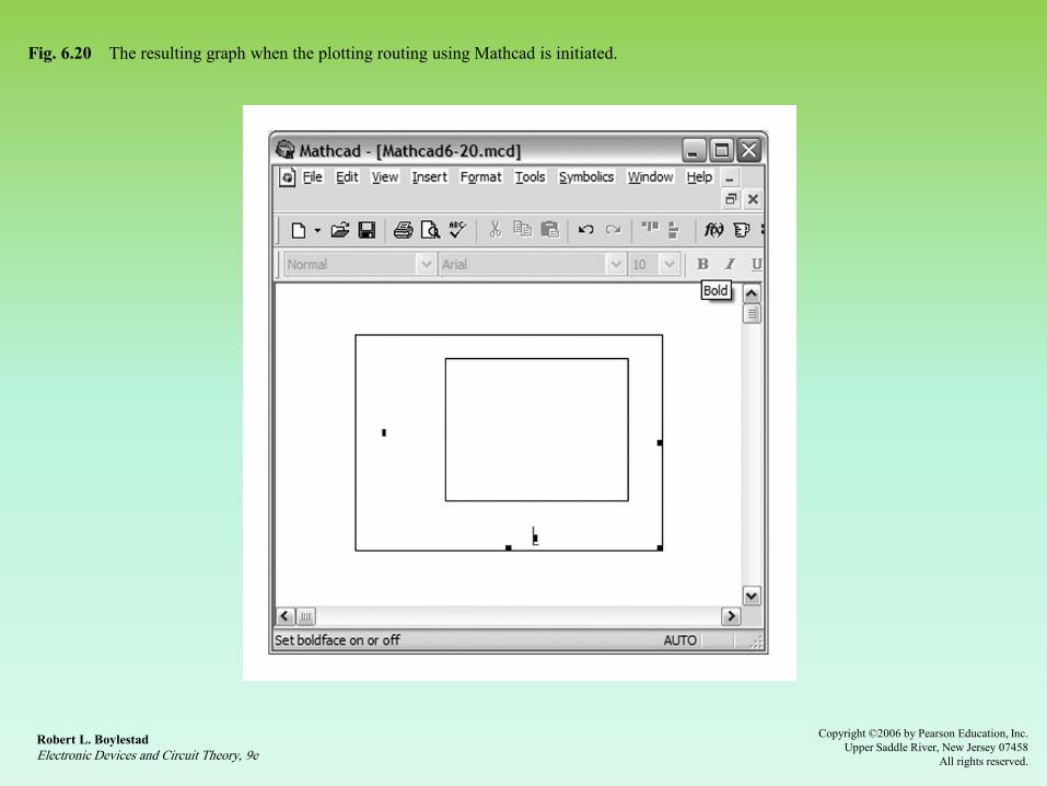
Fig. 6.20 The resulting graph when the plotting routing using Mathcad is initiated.
Robert L. Boylestad
Electronic Devices and Circuit Theory, 9e
Copyright ©2006 by Pearson Education, Inc.
Upper Saddle River, New Jersey 07458
All rights reserved.
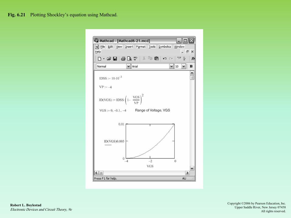
Fig. 6.21 Plotting Shockley’s equation using Mathcad.
Robert L. Boylestad
Electronic Devices and Circuit Theory, 9e
Copyright ©2006 by Pearson Education, Inc.
Upper Saddle River, New Jersey 07458
All rights reserved.

Fig. 6.22 2N5457 Motorola n-channel JFET.
Robert L. Boylestad
Electronic Devices and Circuit Theory, 9e
Copyright ©2006 by Pearson Education, Inc.
Upper Saddle River, New Jersey 07458
All rights reserved.
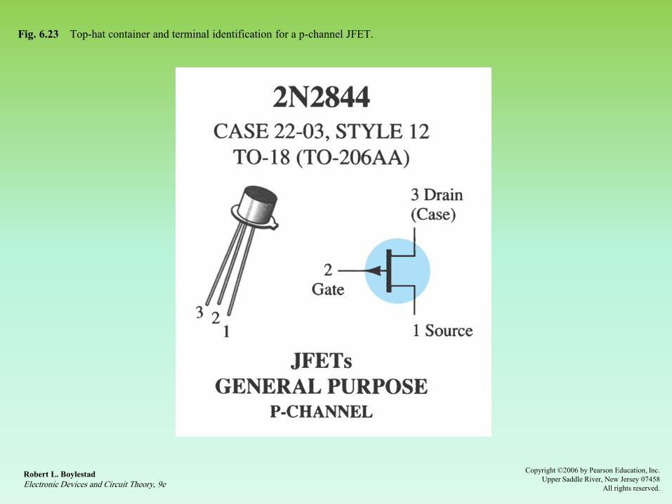
Fig. 6.23 Top-hat container and terminal identification for a p-channel JFET.
Robert L. Boylestad
Electronic Devices and Circuit Theory, 9e
Copyright ©2006 by Pearson Education, Inc.
Upper Saddle River, New Jersey 07458
All rights reserved.

Fig. 6.24 Normal operating region for linear amplifier design.
Robert L. Boylestad
Electronic Devices and Circuit Theory, 9e
Copyright ©2006 by Pearson Education, Inc.
Upper Saddle River, New Jersey 07458
All rights reserved.

Fig. 6.25 Drain characteristics for a 2N4416 JFET transistor as displayed on a curve tracer.
Robert L. Boylestad
Electronic Devices and Circuit Theory, 9e
Copyright ©2006 by Pearson Education, Inc.
Upper Saddle River, New Jersey 07458
All rights reserved.

Fig. 6.26 (a) JFET versus (b) BJT.
Robert L. Boylestad
Electronic Devices and Circuit Theory, 9e
Copyright ©2006 by Pearson Education, Inc.
Upper Saddle River, New Jersey 07458
All rights reserved.
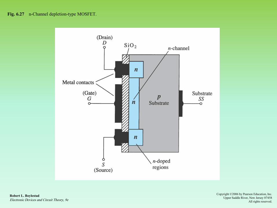
Fig. 6.27 n-Channel depletion-type MOSFET.
Robert L. Boylestad
Electronic Devices and Circuit Theory, 9e
Copyright ©2006 by Pearson Education, Inc.
Upper Saddle River, New Jersey 07458
All rights reserved.
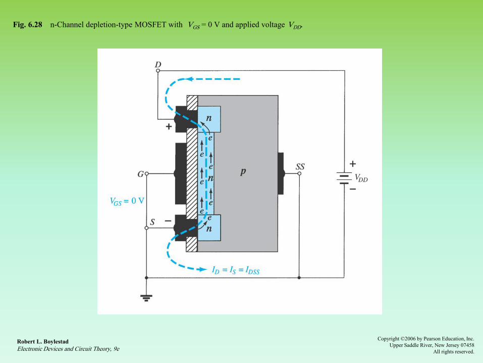
Fig. 6.28 n-Channel depletion-type MOSFET with VGS = 0 V and applied voltage VDD.
Robert L. Boylestad
Electronic Devices and Circuit Theory, 9e
Copyright ©2006 by Pearson Education, Inc.
Upper Saddle River, New Jersey 07458
All rights reserved.

Fig. 6.29 Drain and transfer characteristics for an n-channel depletion-type MOSFET.
Robert L. Boylestad
Electronic Devices and Circuit Theory, 9e
Copyright ©2006 by Pearson Education, Inc.
Upper Saddle River, New Jersey 07458
All rights reserved.

Fig. 6.30 Reduction in free carriers in a channel due to a negative potential at the gate terminal.
Robert L. Boylestad
Electronic Devices and Circuit Theory, 9e
Copyright ©2006 by Pearson Education, Inc.
Upper Saddle River, New Jersey 07458
All rights reserved.

Fig. 6.31 Transfer characteristics for an n-channel depletion-type MOSFET with IDSS = 10 mA and VP = -4 V.
Robert L. Boylestad
Electronic Devices and Circuit Theory, 9e
Copyright ©2006 by Pearson Education, Inc.
Upper Saddle River, New Jersey 07458
All rights reserved.
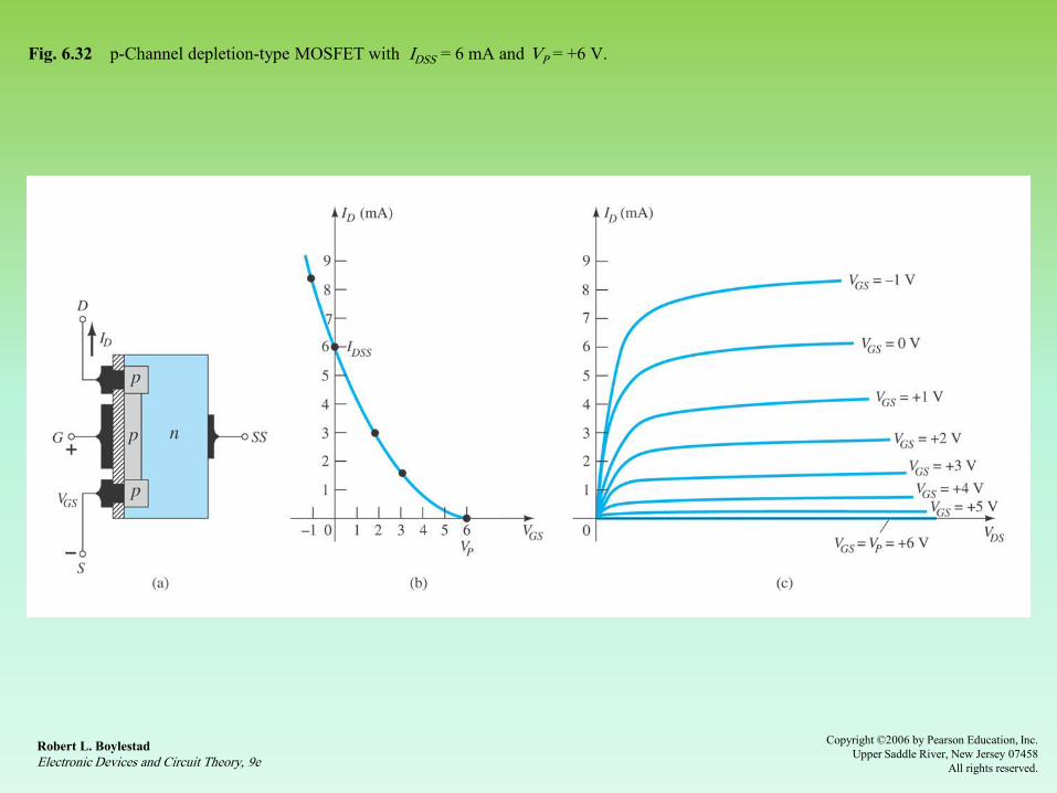
Fig. 6.32 p-Channel depletion-type MOSFET with IDSS = 6 mA and VP = +6 V.
Robert L. Boylestad
Electronic Devices and Circuit Theory, 9e
Copyright ©2006 by Pearson Education, Inc.
Upper Saddle River, New Jersey 07458
All rights reserved.

Fig. 6.33 Graphic symbols for (a) n-channel depletion-type MOSFETs and (b) p-channel depletion-type
MOSFETs.
Robert L. Boylestad
Electronic Devices and Circuit Theory, 9e
Copyright ©2006 by Pearson Education, Inc.
Upper Saddle River, New Jersey 07458
All rights reserved.
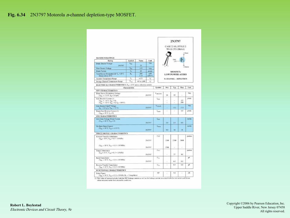
Fig. 6.34 2N3797 Motorola n-channel depletion-type MOSFET.
Robert L. Boylestad
Electronic Devices and Circuit Theory, 9e
Copyright ©2006 by Pearson Education, Inc.
Upper Saddle River, New Jersey 07458
All rights reserved.

Fig. 6.35 n-Channel enhancement-type MOSFET.
Robert L. Boylestad
Electronic Devices and Circuit Theory, 9e
Copyright ©2006 by Pearson Education, Inc.
Upper Saddle River, New Jersey 07458
All rights reserved.
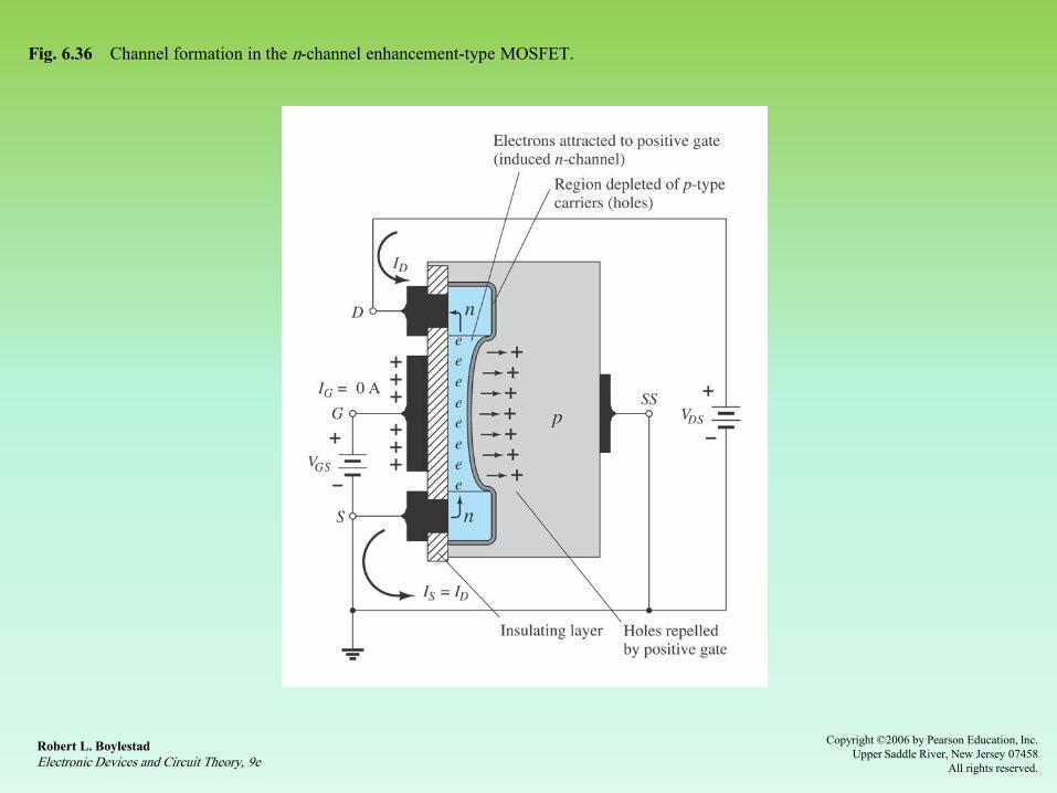
Fig. 6.36 Channel formation in the n-channel enhancement-type MOSFET.
Robert L. Boylestad
Electronic Devices and Circuit Theory, 9e
Copyright ©2006 by Pearson Education, Inc.
Upper Saddle River, New Jersey 07458
All rights reserved.

Fig. 6.37 Change in channel and depletion region with increasing level of VDS for a fixed value of VGS.
Robert L. Boylestad
Electronic Devices and Circuit Theory, 9e
Copyright ©2006 by Pearson Education, Inc.
Upper Saddle River, New Jersey 07458
All rights reserved.

Fig. 6.38 Drain characteristics of an n-channel enhancement-type MOSFET with VT = 2 V and k = 0.278 x 10⁻³
A/V2.
Robert L. Boylestad
Electronic Devices and Circuit Theory, 9e
Copyright ©2006 by Pearson Education, Inc.
Upper Saddle River, New Jersey 07458
All rights reserved.
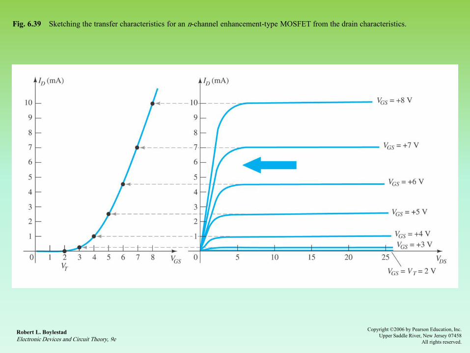
Fig. 6.39 Sketching the transfer characteristics for an n-channel enhancement-type MOSFET from the drain characteristics.
Robert L. Boylestad
Electronic Devices and Circuit Theory, 9e
Copyright ©2006 by Pearson Education, Inc.
Upper Saddle River, New Jersey 07458
All rights reserved.

Fig. 6.40 Plotting the transfer characteristics of an n-channel enhancement-type MOSFET with k = 0.5 x 10⁻³ A/V2 and VT = 4 V.
Robert L. Boylestad
Electronic Devices and Circuit Theory, 9e
Copyright ©2006 by Pearson Education, Inc.
Upper Saddle River, New Jersey 07458
All rights reserved.

Fig. 6.41 p-Channel enhancement-type MOSFET with VT = 2 V and k = 0.5 x 10⁻³ A/V2.
Robert L. Boylestad
Electronic Devices and Circuit Theory, 9e
Copyright ©2006 by Pearson Education, Inc.
Upper Saddle River, New Jersey 07458
All rights reserved.

Fig. 6.42 Symbols for (a) n-channel enhancement-type MOSFETs and (b) p-channel enhancement-type MOSFETs.
Robert L. Boylestad
Electronic Devices and Circuit Theory, 9e
Copyright ©2006 by Pearson Education, Inc.
Upper Saddle River, New Jersey 07458
All rights reserved.

Fig. 6.43 2N4351 Motorola n-channel enhancement-type MOSFET.
Robert L. Boylestad
Electronic Devices and Circuit Theory, 9e
Copyright ©2006 by Pearson Education, Inc.
Upper Saddle River, New Jersey 07458
All rights reserved.

Fig. 6.44 Solution to Example 6.4.
Robert L. Boylestad
Electronic Devices and Circuit Theory, 9e
Copyright ©2006 by Pearson Education, Inc.
Upper Saddle River, New Jersey 07458
All rights reserved.

Fig. 6.45 Zener-protected MOSFET.
Robert L. Boylestad
Electronic Devices and Circuit Theory, 9e
Copyright ©2006 by Pearson Education, Inc.
Upper Saddle River, New Jersey 07458
All rights reserved.

Fig. 6.46 VMOS construction.
Robert L. Boylestad
Electronic Devices and Circuit Theory, 9e
Copyright ©2006 by Pearson Education, Inc.
Upper Saddle River, New Jersey 07458
All rights reserved.

Fig. 6.47 CMOS with the connections indicated in Fig. 6.48.
Robert L. Boylestad
Electronic Devices and Circuit Theory, 9e
Copyright ©2006 by Pearson Education, Inc.
Upper Saddle River, New Jersey 07458
All rights reserved.

Fig. 6.48 CMOS inverter.
Robert L. Boylestad
Electronic Devices and Circuit Theory, 9e
Copyright ©2006 by Pearson Education, Inc.
Upper Saddle River, New Jersey 07458
All rights reserved.

Fig. 6.49 Relative resistance levels for Vi = 5 V(1-state).
Robert L. Boylestad
Electronic Devices and Circuit Theory, 9e
Copyright ©2006 by Pearson Education, Inc.
Upper Saddle River, New Jersey 07458
All rights reserved.

Fig. 6.50 Basic construction of an n-channel MESFET.
Robert L. Boylestad
Electronic Devices and Circuit Theory, 9e
Copyright ©2006 by Pearson Education, Inc.
Upper Saddle River, New Jersey 07458
All rights reserved.
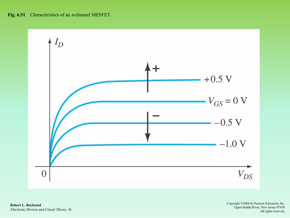
Fig. 6.51 Characteristics of an n-channel MESFET.
Robert L. Boylestad
Electronic Devices and Circuit Theory, 9e
Copyright ©2006 by Pearson Education, Inc.
Upper Saddle River, New Jersey 07458
All rights reserved.

Fig. 6.52 Symbol and basic biasing arrangement for an n-channel MESFET.
Robert L. Boylestad
Electronic Devices and Circuit Theory, 9e
Copyright ©2006 by Pearson Education, Inc.
Upper Saddle River, New Jersey 07458
All rights reserved.

Fig. 6.53 Enhancement-type MESFET: (a) construction; (b) symbol.
Robert L. Boylestad
Electronic Devices and Circuit Theory, 9e
Copyright ©2006 by Pearson Education, Inc.
Upper Saddle River, New Jersey 07458
All rights reserved.

Fig. 6.54 Network used to obtain the characteristics of the n-channel J2N3819 JFET.
Robert L. Boylestad
Electronic Devices and Circuit Theory, 9e
Copyright ©2006 by Pearson Education, Inc.
Upper Saddle River, New Jersey 07458
All rights reserved.

Fig. 6.55 Drain characteristics for the n-channel J2N3819 JFET of Fig. 6.54.
Robert L. Boylestad
Electronic Devices and Circuit Theory, 9e
Copyright ©2006 by Pearson Education, Inc.
Upper Saddle River, New Jersey 07458
All rights reserved.

Fig. 6.56 Transfer characteristics for the n-channel J2N3819 JFET of Fig. 6.54.
Robert L. Boylestad
Electronic Devices and Circuit Theory, 9e
Copyright ©2006 by Pearson Education, Inc.
Upper Saddle River, New Jersey 07458
All rights reserved.

Fig. 6.57 Problems 9 and 17.
Robert L. Boylestad
Electronic Devices and Circuit Theory, 9e
Copyright ©2006 by Pearson Education, Inc.
Upper Saddle River, New Jersey 07458
All rights reserved.
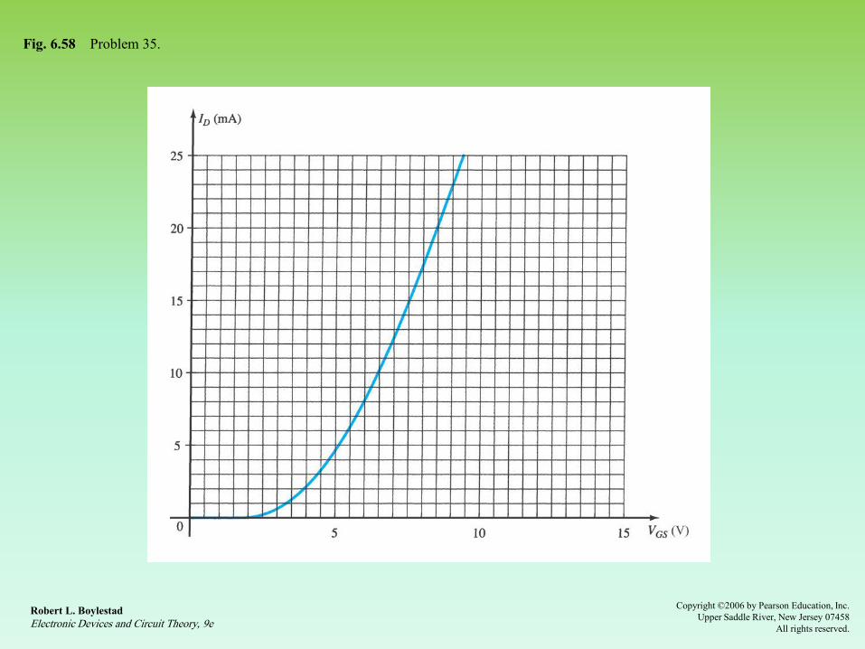
Fig. 6.58 Problem 35.
Robert L. Boylestad
Electronic Devices and Circuit Theory, 9e
Copyright ©2006 by Pearson Education, Inc.
Upper Saddle River, New Jersey 07458
All rights reserved.


![z ]site.iugaza.edu.ps/jarja/files/2015/04/...z ] 1 / s 4 t , k e](https://img.pdfslide.us/doc/110x75/5e306251fc79ed51511e5c02/-z-site-z-1-s-4-t-k-e-.jpg)