Embed Size (px)
Citation preview
Problem-Solving Companion
To accompany
Basic Engineering Circuit Analysis Eight Edition
J. David Irwin Auburn University
JOHN WILEY & SONS, INC.

Executive Editor Bill Zobrist Assistant Editor Kelly Boyle Marketing Manager Frank Lyman Senior Production Editor Jaime Perea Copyright © 2005, John Wiley & Sons, Inc. All rights reserved No part of this publication may be reproduced, stored in a retrieval system or transmitted in any form or by any means, electronic, mechanical, photocopying, recording, scanning, or otherwise, except as permitted under Sections 107 or 108 of the 1976 United States Copyright Act, without either the prior written permission of the Publisher, or authorization through payment of the appropriate per-copy fee to the Copyright Clearance Center, 222 Rosewood Drive, Danvers, MA 01923, (508) 750-8400, fax (508) 750-4470. Requests to the Publisher for permission should be addressed to the Permissions Department, John Wiley & Sons, Inc., 605 Third Avenue, New York, NY 10158-0012, (212) 850-6011, fax (212)850-6008, e-mail: [email protected]. ISBN 0-471-74026-8
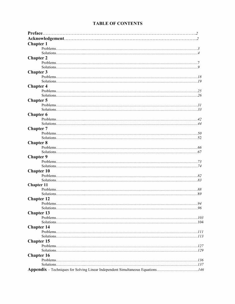
TABLE OF CONTENTS Preface……………………………………………………………………………………….2 Acknowledgement…………………..……………………………………………………….2 Chapter 1 Problems…………………..……………………………….……………………………………………3 Solutions…………………..…………………………………………………….………………………4 Chapter 2 Problems…………………..…………………………………………………….………………………7 Solutions…………………..…………………………………………………….………………………9 Chapter 3 Problems…………………..…………………………………………………….………………………18 Solutions…………………..…………………………………………………….………………………19 Chapter 4 Problems…………………..…………………………………………………….………………………25 Solutions…………………..…………………………………………………….………………………26 Chapter 5 Problems…………………..…………………………………………………….………………………31 Solutions…………………..…………………………………………………….………………………33 Chapter 6 Problems…………………..…………………………………………………….………………………42 Solutions…………………..…………………………………………………….………………………44 Chapter 7 Problems…………………..…………………………………………………….………………………50 Solutions…………………..…………………………………………………….………………………52 Chapter 8 Problems…………………..…………………………………………………….………………………66 Solutions…………………..…………………………………………………….………………………67 Chapter 9 Problems…………………..…………………………………………………….………………………73 Solutions…………………..…………………………………………………….………………………74 Chapter 10 Problems…………………..…………………………………………………….………………………82 Solutions…………………..…………………………………………………….………………………83 Chapter 11 Problems…………………..…………………………………………………….………………………88 Solutions…………………..…………………………………………………….………………………89 Chapter 12 Problems…………………..…………………………………………………….………………………94 Solutions…………………..…………………………………………………….………………………96 Chapter 13 Problems…………………..…………………………………………………….………………………103 Solutions…………………..…………………………………………………….………………………104 Chapter 14 Problems…………………..…………………………………………………….………………………111 Solutions…………………..…………………………………………………….………………………113 Chapter 15 Problems…………………..…………………………………………………….………………………127 Solutions…………………..…………………………………………………….………………………129 Chapter 16 Problems…………………..…………………………………………………….………………………136 Solutions…………………..…………………………………………………….………………………137 Appendix – Techniques for Solving Linear Independent Simultaneous Equations…………………………...146

2
STUDENT PROBLEM COMPANION
To Accompany
BASIC ENGINEERING CIRCUIT ANALYSIS, EIGHTH EDITION By
J. David Irwin and R. Mark Nelms PREFACE This Student Problem Companion is designed to be used in conjunction with Basic
Engineering Circuit Analysis, 8e, authored by J. David Irwin and R. Mark Nelms and published by John Wiley & Sons, Inc.. The material tracts directly the chapters in the book and is organized in the following manner. For each chapter there is a set of problems that are representative of the end-of-chapter problems in the book. Each of the problem sets could be thought of as a mini-quiz on the particular chapter. The student is encouraged to try to work the problems first without any aid. If they are unable to work the problems for any reason, the solutions to each of the problem sets are also included. An analysis of the solution will hopefully clarify any issues that are not well understood. Thus this companion document is prepared as a helpful adjunct to the book.
3
CHAPTER 1 PROBLEMS 1.1 Determine whether the element in Fig. 1.1 is absorbing or supplying power and how
much. -2A
+
-
12V
Fig. 1.1
1.2 In Fig. 1.2, element 2 absorbs 24W of power. Is element 1 absorbing or supplying power
and how much.
+
-
12V
-
+
6V
Fig. 1.2
1.3. Given the network in Fig.1.3 find the value of the unknown voltage VX.
1 2
3+-
+-
+
-
+ - + -4V 10V2A
2A4A
8V12V
6A
VX
Fig. 1.3
4
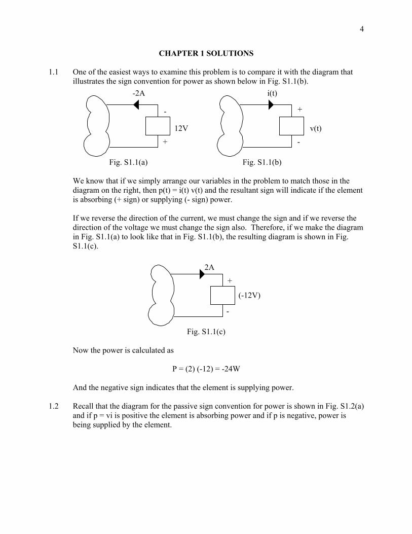
CHAPTER 1 SOLUTIONS 1.1 One of the easiest ways to examine this problem is to compare it with the diagram that
illustrates the sign convention for power as shown below in Fig. S1.1(b). -2A
+
-
12V
i(t)
+
-
v(t)
Fig. S1.1(a) Fig. S1.1(b) We know that if we simply arrange our variables in the problem to match those in the
diagram on the right, then p(t) = i(t) v(t) and the resultant sign will indicate if the element is absorbing (+ sign) or supplying (- sign) power.
If we reverse the direction of the current, we must change the sign and if we reverse the
direction of the voltage we must change the sign also. Therefore, if we make the diagram in Fig. S1.1(a) to look like that in Fig. S1.1(b), the resulting diagram is shown in Fig. S1.1(c).
2A
+
-
(-12V)
Fig. S1.1(c)
Now the power is calculated as
P = (2) (-12) = -24W And the negative sign indicates that the element is supplying power. 1.2 Recall that the diagram for the passive sign convention for power is shown in Fig. S1.2(a)
and if p = vi is positive the element is absorbing power and if p is negative, power is being supplied by the element.
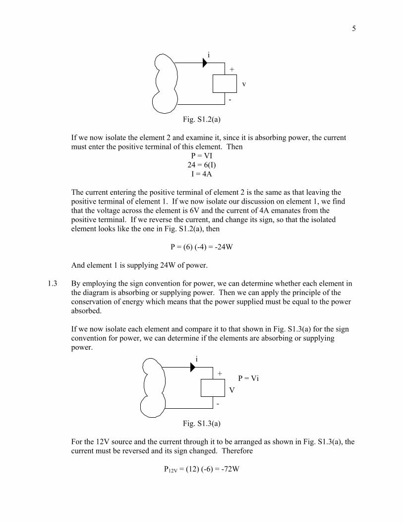
5
i
+
-
v
Fig. S1.2(a)
If we now isolate the element 2 and examine it, since it is absorbing power, the current
must enter the positive terminal of this element. Then P = VI
24 = 6(I) I = 4A
The current entering the positive terminal of element 2 is the same as that leaving the
positive terminal of element 1. If we now isolate our discussion on element 1, we find that the voltage across the element is 6V and the current of 4A emanates from the positive terminal. If we reverse the current, and change its sign, so that the isolated element looks like the one in Fig. S1.2(a), then
P = (6) (-4) = -24W
And element 1 is supplying 24W of power. 1.3 By employing the sign convention for power, we can determine whether each element in
the diagram is absorbing or supplying power. Then we can apply the principle of the conservation of energy which means that the power supplied must be equal to the power absorbed.
If we now isolate each element and compare it to that shown in Fig. S1.3(a) for the sign
convention for power, we can determine if the elements are absorbing or supplying power.
i
+
-
VP = Vi
Fig. S1.3(a)
For the 12V source and the current through it to be arranged as shown in Fig. S1.3(a), the
current must be reversed and its sign changed. Therefore
P12V = (12) (-6) = -72W
6
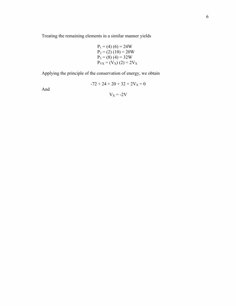
Treating the remaining elements in a similar manner yields P1 = (4) (6) = 24W P2 = (2) (10) = 20W P3 = (8) (4) = 32W PVX = (VX) (2) = 2VX Applying the principle of the conservation of energy, we obtain
-72 + 24 + 20 + 32 + 2VX = 0 And
VX = -2V
7
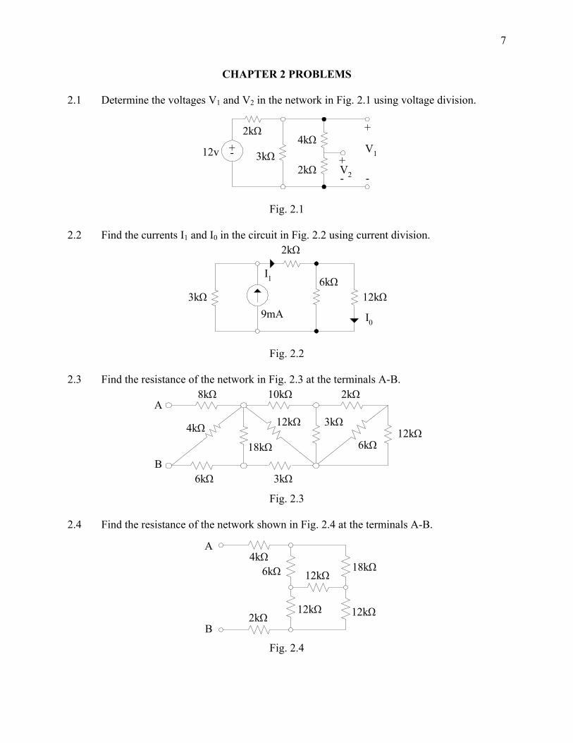
CHAPTER 2 PROBLEMS 2.1 Determine the voltages V1 and V2 in the network in Fig. 2.1 using voltage division.
2kΩ
3kΩ2kΩ
4kΩ12v +-
+
+
- -
V1
V2
Fig. 2.1
2.2 Find the currents I1 and I0 in the circuit in Fig. 2.2 using current division.
3kΩ
2kΩ
6kΩ12kΩ
9mA I0
I1
Fig. 2.2 2.3 Find the resistance of the network in Fig. 2.3 at the terminals A-B.
A
B
8kΩ 10kΩ 2kΩ
4kΩ
18kΩ
6kΩ 3kΩ
3kΩ
6kΩ12kΩ
12kΩ
Fig. 2.3
2.4 Find the resistance of the network shown in Fig. 2.4 at the terminals A-B.
A
B
4kΩ6kΩ
2kΩ
12kΩ
12kΩ 12kΩ
18kΩ
Fig. 2.4
8
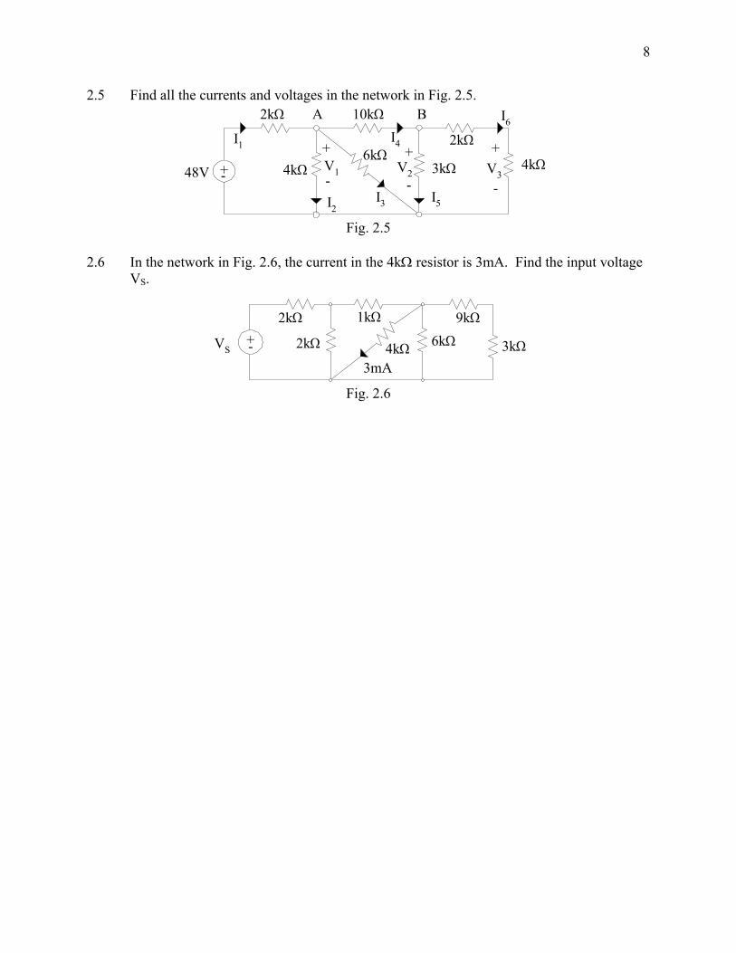
2.5 Find all the currents and voltages in the network in Fig. 2.5. 2kΩ 10kΩ
2kΩ
48V 4kΩ 3kΩ 4kΩ6kΩ
I1
V1 V2 V3
I2
I4
A B
I3 I5
I6
+
-
+ +
- -+-
Fig. 2.5
2.6 In the network in Fig. 2.6, the current in the 4kΩ resistor is 3mA. Find the input voltage
VS.
2kΩ 1kΩ
VS 4kΩ3mA
6kΩ 3kΩ2kΩ
9kΩ+-
Fig. 2.6
9
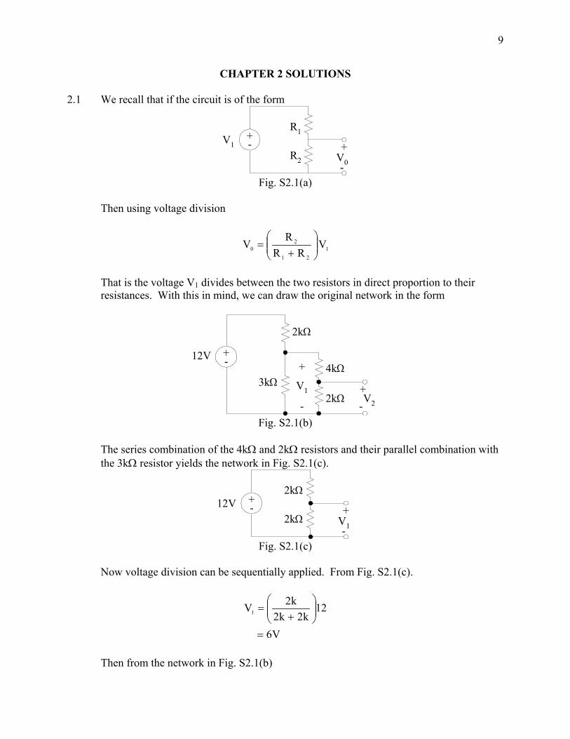
CHAPTER 2 SOLUTIONS 2.1 We recall that if the circuit is of the form
V1
R1
R2 V0
+- +
- Fig. S2.1(a)
Then using voltage division
121
20 V
RRR
V ⎟⎟⎠
⎞⎜⎜⎝
⎛+
=
That is the voltage V1 divides between the two resistors in direct proportion to their
resistances. With this in mind, we can draw the original network in the form
V1
2kΩ
V2
12V +- +
-
3kΩ4kΩ
2kΩ-+
Fig. S2.1(b)
The series combination of the 4kΩ and 2kΩ resistors and their parallel combination with
the 3kΩ resistor yields the network in Fig. S2.1(c).
12V2kΩ
V1
+- +
-2kΩ
Fig. S2.1(c)
Now voltage division can be sequentially applied. From Fig. S2.1(c).
V6
12k2k2
k2V1
=
⎟⎟⎠
⎞⎜⎜⎝
⎛+
=
Then from the network in Fig. S2.1(b)
10
V2
Vk4k2
k2V 12
=
⎟⎟⎠
⎞⎜⎜⎝
⎛+
=
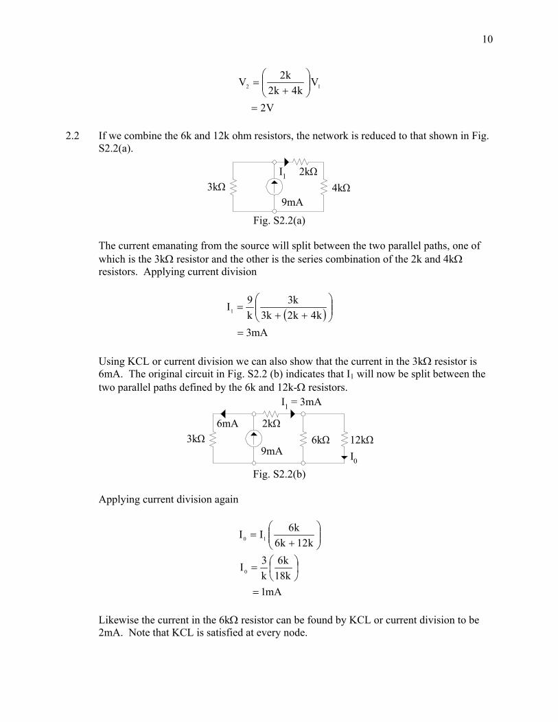
2.2 If we combine the 6k and 12k ohm resistors, the network is reduced to that shown in Fig.
S2.2(a).
3kΩ2kΩ
4kΩ9mA
I1
Fig. S2.2(a)
The current emanating from the source will split between the two parallel paths, one of
which is the 3kΩ resistor and the other is the series combination of the 2k and 4kΩ resistors. Applying current division
( )mA3
k4k2k3k3
k9I1
=
⎟⎟⎠
⎞⎜⎜⎝
⎛++
=
Using KCL or current division we can also show that the current in the 3kΩ resistor is
6mA. The original circuit in Fig. S2.2 (b) indicates that I1 will now be split between the two parallel paths defined by the 6k and 12k-Ω resistors.
3kΩ2kΩ
6kΩ9mA
I1 = 3mA
6mA12kΩI0
Fig. S2.2(b) Applying current division again
⎟⎟⎠
⎞⎜⎜⎝
⎛+
=k12k6
k6II 10
mA1
k18k6
k3I0
=
⎟⎠⎞
⎜⎝⎛=
Likewise the current in the 6kΩ resistor can be found by KCL or current division to be
2mA. Note that KCL is satisfied at every node.
11
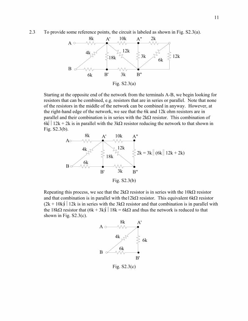
2.3 To provide some reference points, the circuit is labeled as shown in Fig. S2.3(a).
A
B
8k 10k 2k
4k18k
6k 3k
3k6k
12k12k
A' A"
B' B"
Fig. S2.3(a) Starting at the opposite end of the network from the terminals A-B, we begin looking for
resistors that can be combined, e.g. resistors that are in series or parallel. Note that none of the resistors in the middle of the network can be combined in anyway. However, at the right-hand edge of the network, we see that the 6k and 12k ohm resistors are in parallel and their combination is in series with the 2kΩ resistor. This combination of 6k⎪⎢12k + 2k is in parallel with the 3kΩ resistor reducing the network to that shown in Fig. S2.3(b).
A
B
8k 10k
2k = 3k (6k 12k + 2k)4k
18k6k
3k
12k
A' A"
B' B"
Fig. S2.3(b) Repeating this process, we see that the 2kΩ resistor is in series with the 10kΩ resistor
and that combination is in parallel with the12kΩ resistor. This equivalent 6kΩ resistor (2k + 10k)⎪⎢12k is in series with the 3kΩ resistor and that combination is in parallel with the 18kΩ resistor that (6k + 3k)⎪⎢18k = 6kΩ and thus the network is reduced to that shown in Fig. S2.3(c).
A
B
8k
4k6k
6k
A'
B'
Fig. S2.3(c)

12
At this point we see that the two 6kΩ resistors are in series and their combination in parallel with the 4kΩ resistor. This combination (6k + 6k)⎪⎢4k = 3kΩ which is in series with 8kΩ resistors yielding A total resistance RAB = 3k + 8k = 11kΩ.
2.4 An examination of the network indicates that there are no series or parallel combinations
of resistors in this network. However, if we redraw the network in the form shown in Fig. S2.4(a), we find that the networks have two deltas back to back.
A
B
4k
2k 12k 12k
12k6k 18k
Fig. S2.4(a)
If we apply the ∆→Y transformation to either delta, the network can be reduced to a
circuit in which the various resistors are either in series or parallel. Employing the ∆→Y transformation to the upper delta, we find the new elements using the following equations as illustrated in Fig. S2.4(b)
12k
R1
6k 18k
R3R2
Fig. S2.4(b)
( ) ( )
Ω=++
= k3k18k12k6
k18k6R1
( ) ( )Ω=
++= k2
k18k12k6k12k6R 2
( ) ( )Ω=
++= k6
k18k12k6k18k12R 3
The network is now reduced to that shown in Fig. S2.4(c).
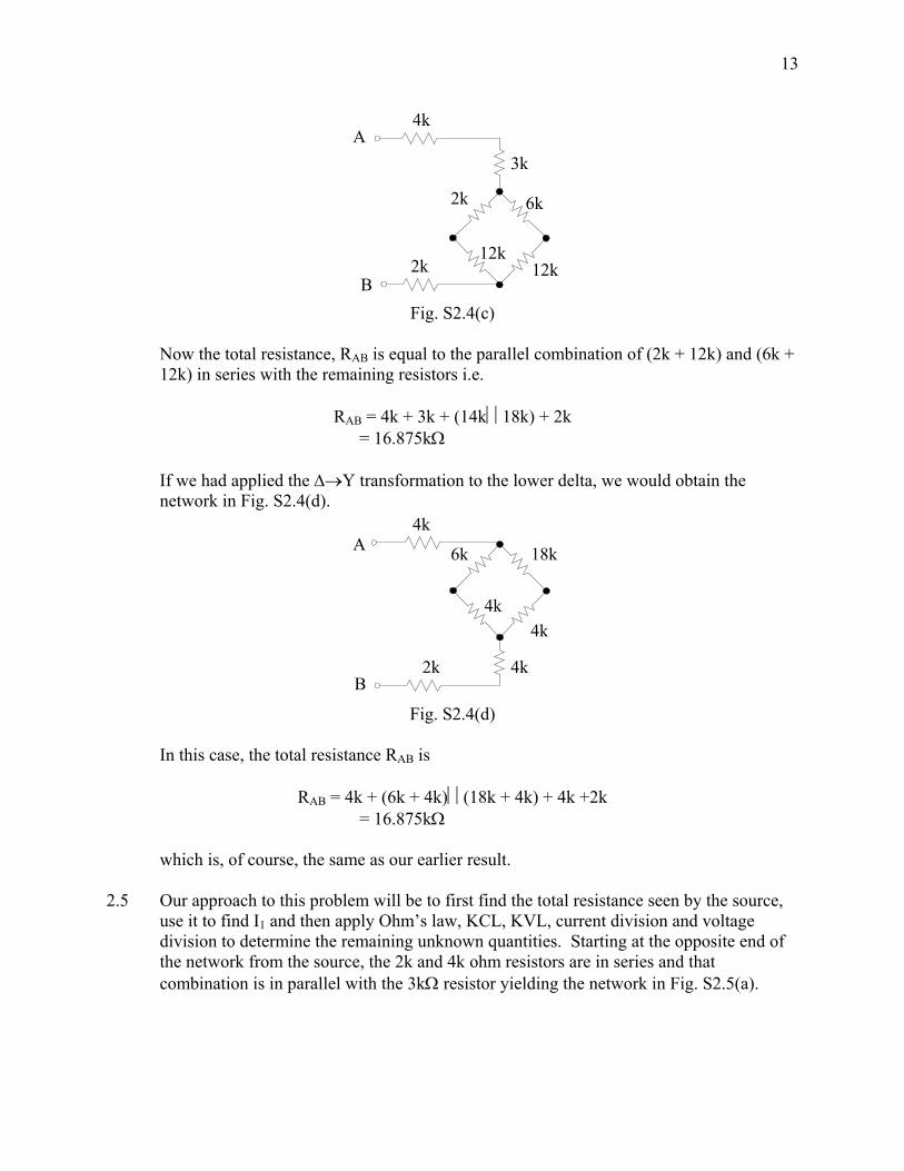
13
A
B
4k
2k12k
12k
3k
2k 6k
Fig. S2.4(c)
Now the total resistance, RAB is equal to the parallel combination of (2k + 12k) and (6k +
12k) in series with the remaining resistors i.e.
RAB = 4k + 3k + (14k⎪⎢18k) + 2k = 16.875kΩ If we had applied the ∆→Y transformation to the lower delta, we would obtain the
network in Fig. S2.4(d).
A
B
4k
2k
4k4k
4k
6k 18k
Fig. S2.4(d)
In this case, the total resistance RAB is
RAB = 4k + (6k + 4k)⎪⎢(18k + 4k) + 4k +2k = 16.875kΩ which is, of course, the same as our earlier result. 2.5 Our approach to this problem will be to first find the total resistance seen by the source,
use it to find I1 and then apply Ohm’s law, KCL, KVL, current division and voltage division to determine the remaining unknown quantities. Starting at the opposite end of the network from the source, the 2k and 4k ohm resistors are in series and that combination is in parallel with the 3kΩ resistor yielding the network in Fig. S2.5(a).
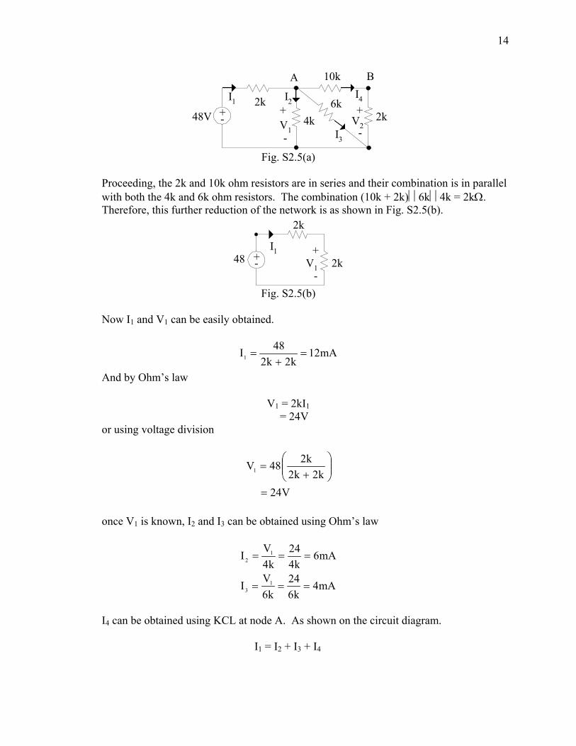
14
A B
2k
10k
V14k48V
6kI1 I2
I3
I4
2k+-+
-
+
-V2
Fig. S2.5(a)
Proceeding, the 2k and 10k ohm resistors are in series and their combination is in parallel
with both the 4k and 6k ohm resistors. The combination (10k + 2k)⎪⎢6k⎪⎢4k = 2kΩ. Therefore, this further reduction of the network is as shown in Fig. S2.5(b).
2k
2k48+
-V1
I1+-
Fig. S2.5(b)
Now I1 and V1 can be easily obtained.
mA12k2k2
48I1 =+
=
And by Ohm’s law
V1 = 2kI1 = 24V or using voltage division
V24k2k2
k248V1
=
⎟⎟⎠
⎞⎜⎜⎝
⎛+
=
once V1 is known, I2 and I3 can be obtained using Ohm’s law
mA6k4
24k4
VI 12 ===
mA4k6
24k6
VI 13 ===
I4 can be obtained using KCL at node A. As shown on the circuit diagram. I1 = I2 + I3 + I4
15
4Ik4
k6
k12
++=
mA2k2I4 ==
The voltage V2 is then V2 = V1 - 10kI4
( ) ⎟⎠⎞
⎜⎝⎛−=
k2k1024
= 4V or using voltage division
V46124
k2k10k2VV 12
=
⎟⎠⎞
⎜⎝⎛=
⎟⎟⎠
⎞⎜⎜⎝
⎛+
=
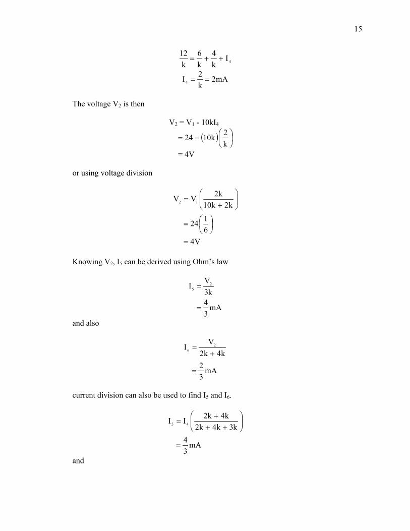
Knowing V2, I5 can be derived using Ohm’s law
mA34
k3V
I 25
=
=
and also
mA32
k4k2VI 2
6
=
+=
current division can also be used to find I5 and I6.
mA34
k3k4k2k4k2II 45
=
⎟⎟⎠
⎞⎜⎜⎝
⎛++
+=
and
16
mA32
k4k2k3k3II 46
=
⎟⎟⎠
⎞⎜⎜⎝
⎛++
=
Finally V3 can be obtained using KVL or voltage division
V38
k32k24
kI2VV 623
=
⎟⎠⎞
⎜⎝⎛−=
−=
and
V38
k2k4k4VV 23
=
⎟⎟⎠
⎞⎜⎜⎝
⎛+
=
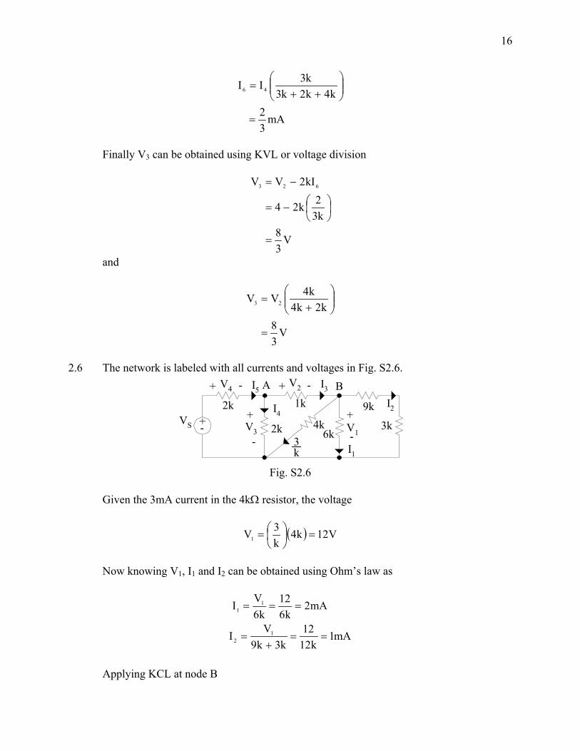
2.6 The network is labeled with all currents and voltages in Fig. S2.6.
A B
4k6k
3k
9k1k
2k
2k
V1
V2
V3
V4
VS
I1
I2
I3
I4
I5
+-+
-
+
-
+ - + -
3k
Fig. S2.6
Given the 3mA current in the 4kΩ resistor, the voltage
( ) V12k4k3V1 =⎟
⎠⎞
⎜⎝⎛=
Now knowing V1, I1 and I2 can be obtained using Ohm’s law as
mA2k6
12k6
VI 11 ===
mA1k12
12k3k9
VI 12 ==
+=
Applying KCL at node B
17
mA6
IIk3I 213
=
++=
Then using Ohm’s law
V2 = I3 (1k) = 6V
KVL can then be used to obtain V3 i.e.
V3 = V2 + V1 = 6 + 12 = 18V Then
mA9k2
VI 3
4
=
=
And
mA15k9
k6
III 435
=
+=
+=
using Ohm’s law
V4 = (2k) I5 = 30V and finally
VS = V4 + V3 = 48V
18
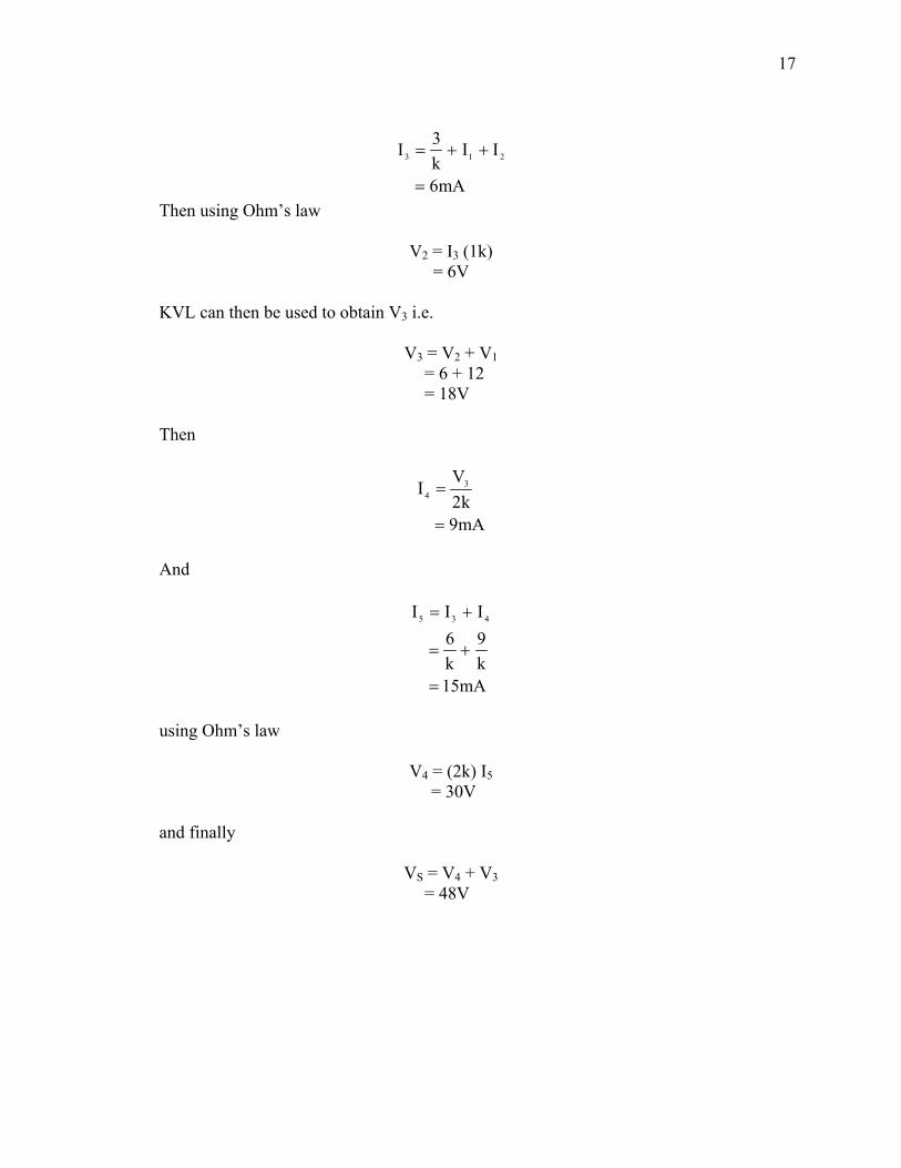
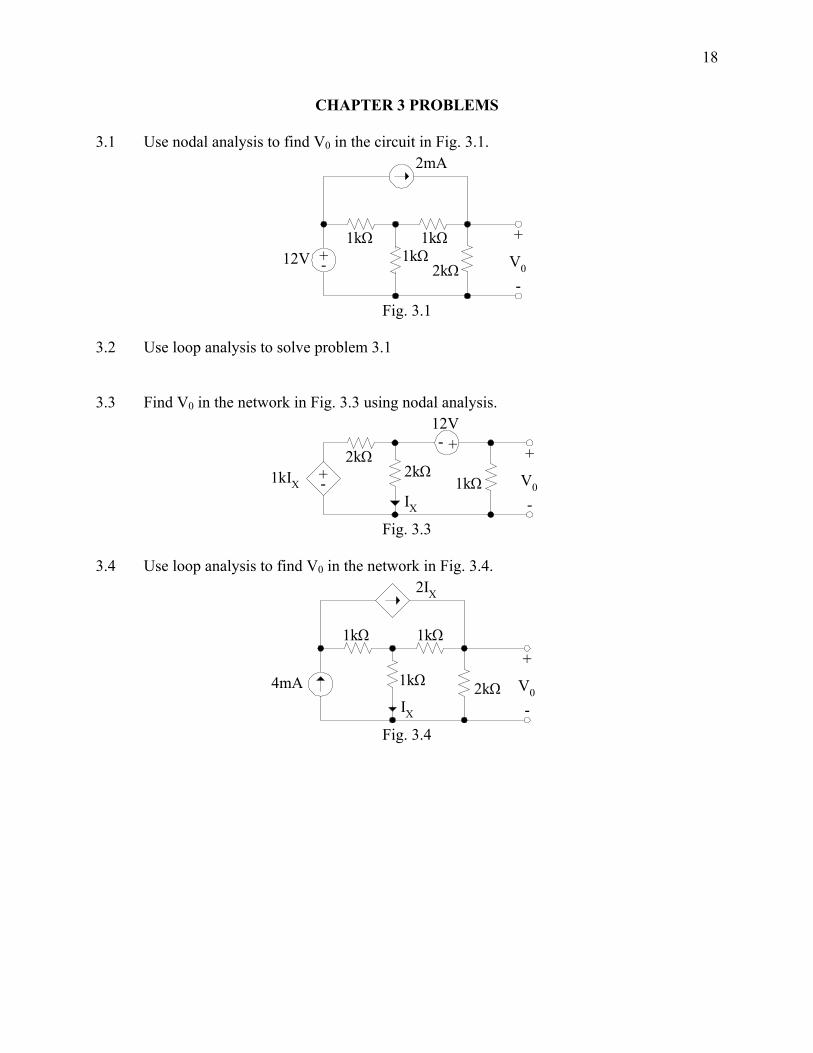
CHAPTER 3 PROBLEMS 3.1 Use nodal analysis to find V0 in the circuit in Fig. 3.1.
+-
+
-
1kΩ 1kΩ1kΩ
2kΩ
2mA
V012V
Fig. 3.1
3.2 Use loop analysis to solve problem 3.1 3.3 Find V0 in the network in Fig. 3.3 using nodal analysis.
+
-
2kΩ
12V
2kΩ1kΩ V0
1kIX
- +
+-IX
Fig. 3.3 3.4 Use loop analysis to find V0 in the network in Fig. 3.4.
4mA+
-
1kΩ 1kΩ
1kΩ 2kΩ V0
2IX
IX Fig. 3.4
19
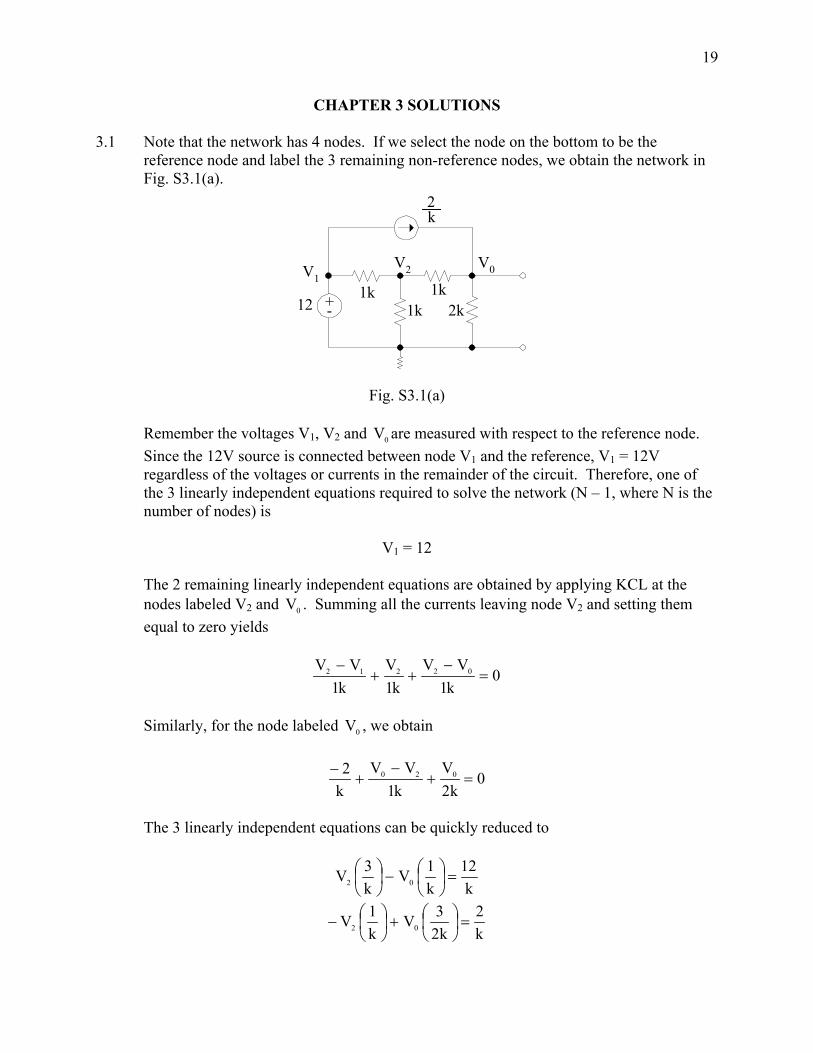
CHAPTER 3 SOLUTIONS 3.1 Note that the network has 4 nodes. If we select the node on the bottom to be the
reference node and label the 3 remaining non-reference nodes, we obtain the network in Fig. S3.1(a).
+-1k 1k
1k 2k
V0
12
V2V1
2k
Fig. S3.1(a)
Remember the voltages V1, V2 and 0V are measured with respect to the reference node.
Since the 12V source is connected between node V1 and the reference, V1 = 12V regardless of the voltages or currents in the remainder of the circuit. Therefore, one of the 3 linearly independent equations required to solve the network (N – 1, where N is the number of nodes) is
V1 = 12
The 2 remaining linearly independent equations are obtained by applying KCL at the
nodes labeled V2 and 0V . Summing all the currents leaving node V2 and setting them equal to zero yields
0k1
VVk1
Vk1
VV 02212 =−
++−
Similarly, for the node labeled 0V , we obtain
0k2
Vk1
VVk2 020 =+
−+
−
The 3 linearly independent equations can be quickly reduced to
k12
k1V
k3V 02 =⎟
⎠⎞
⎜⎝⎛−⎟
⎠⎞
⎜⎝⎛
k2
k23V
k1V 02 =⎟
⎠⎞
⎜⎝⎛+⎟
⎠⎞
⎜⎝⎛−
20
or
3V2 – 0V = 12
2V23V 02 =+−
Solving these equations using any convenient method yields V2 = 740 V and 0V =
736 V.
We can quickly check the accuracy of our calculations. Fig. S3.1(b) illustrates the circuit and the quantities that are currently known.
+-1k 1k
1k 2k
I2
147k
A
847 V
I4
I3
I1
407
V367
V
Fig. S3.1(b)
All unknown branch currents can be easily calculated as follows.
Ak7
44k1
740
784
I1 =−
=
Ak7
40k1740
I2 ==
Ak74
k1736
740
I3 =−
=
Ak7
18k2736
I4 ==
KCL is satisfied at every node and thus we are confident that our calculations are correct. 3.2 The network contains 3 “window panes” and therefore 3 linearly independent loop
equations will be required to determine the unknown currents and voltages. To begin we arbitrarily assign the loop currents as shown in Fig. S3.2.
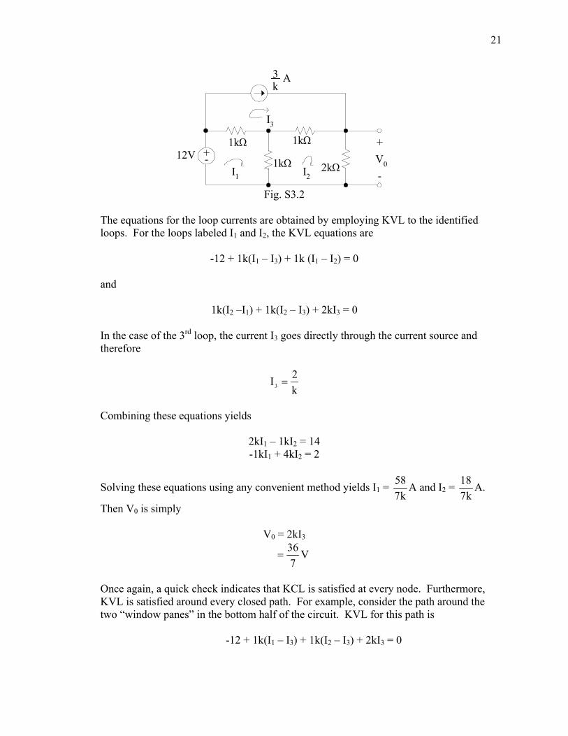
21
+-1kΩ 1kΩ
1kΩ 2kΩV0
12V
I3
I1 I2
+
-
3k
A
Fig. S3.2
The equations for the loop currents are obtained by employing KVL to the identified
loops. For the loops labeled I1 and I2, the KVL equations are
-12 + 1k(I1 – I3) + 1k (I1 – I2) = 0 and
1k(I2 –I1) + 1k(I2 – I3) + 2kI3 = 0 In the case of the 3rd loop, the current I3 goes directly through the current source and
therefore
k2I3 =
Combining these equations yields
2kI1 – 1kI2 = 14 -1kI1 + 4kI2 = 2
Solving these equations using any convenient method yields I1 = k7
58 A and I2 = k7
18 A.
Then V0 is simply
V0 = 2kI3
V736
=
Once again, a quick check indicates that KCL is satisfied at every node. Furthermore,
KVL is satisfied around every closed path. For example, consider the path around the two “window panes” in the bottom half of the circuit. KVL for this path is
-12 + 1k(I1 – I3) + 1k(I2 – I3) + 2kI3 = 0
22
0k7
18k2k7
14k7
18k1k7
14k7
58k112 =⎟⎠⎞
⎜⎝⎛+⎟
⎠⎞
⎜⎝⎛ −+⎟
⎠⎞
⎜⎝⎛ −+−
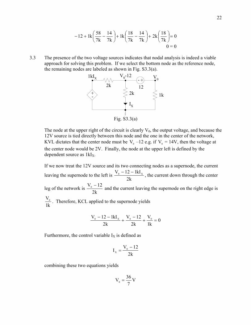
0 = 0 3.3 The presence of the two voltage sources indicates that nodal analysis is indeed a viable
approach for solving this problem. If we select the bottom node as the reference node, the remaining nodes are labeled as shown in Fig. S3.3(a).
+-
1kIX
2k
V0-12+-
1k2k
IX
V0
12
Fig. S3.3(a)
The node at the upper right of the circuit is clearly V0, the output voltage, and because the
12V source is tied directly between this node and the one in the center of the network, KVL dictates that the center node must be 0V –12 e.g. if 0V = 14V, then the voltage at the center node would be 2V. Finally, the node at the upper left is defined by the dependent source as 1kIX.
If we now treat the 12V source and its two connecting nodes as a supernode, the current
leaving the supernode to the left is k2
kI112V X0 −−, the current down through the center
leg of the network is k2
12V0 − and the current leaving the supernode on the right edge is
k1V0 . Therefore, KCL applied to the supernode yields
0k1
Vk2
12Vk2
kI112V 00X0 =+−
+−−
Furthermore, the control variable IX is defined as
k212V
I 0X
−=
combining these two equations yields
V736V0 =
23
The voltages at the remaining non-reference nodes are
V748
784
73612
73612V0
−=−=−=−
And
V724
k2748
k1k2
12Vk1kI1 0
X
−=
⎟⎟⎟⎟
⎠
⎞
⎜⎜⎜⎜
⎝
⎛ −
=⎟⎠⎞
⎜⎝⎛ −
=
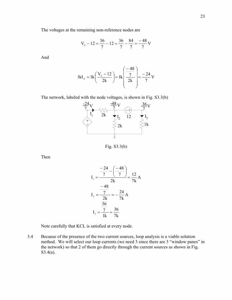
The network, labeled with the node voltages, is shown in Fig. S3.3(b)
+-
2k+-
1k2k
I1 12I2I3
-487 V-24
7 V 367 V
Fig. S3.3(b)
Then
Ak7
12k2
748
724
I1 =⎟⎠⎞
⎜⎝⎛ −
−−
=
Ak7
24k2
748
I2 −=
−
=
k7
36k1
736
I3 ==
Note carefully that KCL is satisfied at every node. 3.4 Because of the presence of the two current sources, loop analysis is a viable solution
method. We will select our loop currents (we need 3 since there are 3 “window panes” in the network) so that 2 of them go directly through the current sources as shown in Fig. S3.4(a).
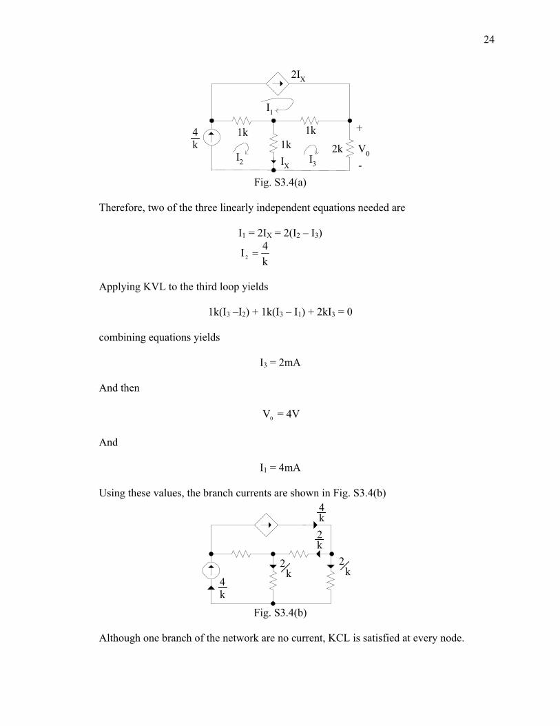
24
1k 1k1k 2k V0
I1
I2 I3
+
-
4k
IX
2IX
Fig. S3.4(a)
Therefore, two of the three linearly independent equations needed are
I1 = 2IX = 2(I2 – I3)
k4I2 =
Applying KVL to the third loop yields
1k(I3 –I2) + 1k(I3 – I1) + 2kI3 = 0 combining equations yields
I3 = 2mA And then
0V = 4V And
I1 = 4mA Using these values, the branch currents are shown in Fig. S3.4(b)
2
4k
k
k2
2k
k4
Fig. S3.4(b)
Although one branch of the network are no current, KCL is satisfied at every node.
25
CHAPTER 4 PROBLEMS 4.1 Derive the gain equation for the nonideal noninverting op-amp configuration and show
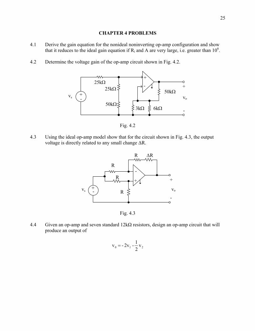
that it reduces to the ideal gain equation if Ri and A are very large, i.e. greater than 106. 4.2 Determine the voltage gain of the op-amp circuit shown in Fig. 4.2.
+
-
25kΩ
50kΩ
6kΩ3kΩ50kΩ
25kΩ
vovs
+-
+-
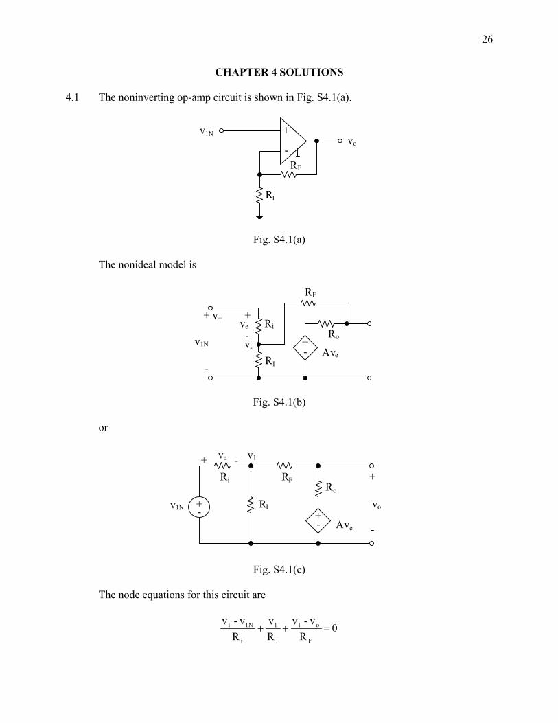
Fig. 4.2 4.3 Using the ideal op-amp model show that for the circuit shown in Fig. 4.3, the output
voltage is directly related to any small change ∆R.
+
-
R
∆RR
R
R vovs
+
-
+-
Fig. 4.3 4.4 Given an op-amp and seven standard 12kΩ resistors, design an op-amp circuit that will
produce an output of
210 v21 - 2v- v =
26
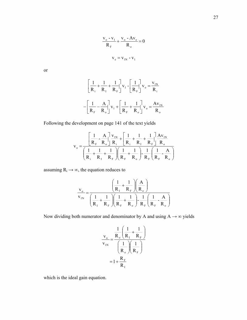
CHAPTER 4 SOLUTIONS 4.1 The noninverting op-amp circuit is shown in Fig. S4.1(a).
vo
v1N
RF
RI
+
-
Fig. S4.1(a) The nonideal model is
+
-RI
v-v1N
v+ ve Ri
Ave
Ro
RF
+
- +-
Fig. S4.1(b) or
+ -
RI vov1N
+
-
ve v1
Ri
Ave
Ro
RF
+- +
-
Fig. S4.1(c) The node equations for this circuit are
0 R
v- v
Rv
Rv- v
F
o1
I
1
i
1N1 =++
27
0 R
Av -v
R v- v
o
eo
F
1o =+
11Ne v- v v =
or
i
1No
F1
FIi Rv
vR1 - v
R1
R1
R1
=⎥⎦
⎤⎢⎣
⎡⎥⎦
⎤⎢⎣
⎡++
o
1No
oF1
oF RAv
vR1
R1 v
RA
R1
=⎥⎦
⎤⎢⎣
⎡++⎥
⎦
⎤⎢⎣
⎡−−
Following the development on page 141 of the text yields
⎟⎟⎠
⎞⎜⎜⎝
⎛⎟⎟⎠
⎞⎜⎜⎝
⎛+⎟⎟
⎠
⎞⎜⎜⎝
⎛++
⎥⎦
⎤⎢⎣
⎡+++⎥
⎦
⎤⎢⎣
⎡
=
oFFoFFIi
o
1N
FIii
1N
oFo
RA -
R1
R1 -
R1
R1
R1
R1
R1
RAv
R1
R1
R1
Rv
RA -
R1
v
assuming Ri → ∞, the equation reduces to
⎟⎟⎠
⎞⎜⎜⎝
⎛⎟⎟⎠
⎞⎜⎜⎝
⎛+⎟⎟
⎠
⎞⎜⎜⎝
⎛+
⎟⎟⎠
⎞⎜⎜⎝
⎛⎟⎟⎠
⎞⎜⎜⎝
⎛+
=
oFFoFFI
oFI
N1
o
RA -
R1
R1 -
R1
R1
R1
R1
RA
R1
R1
vv
Now dividing both numerator and denominator by A and using A → ∞ yields
I
F
Fo
FIo
N1
o
RR 1
R1
R1
R1
R1
R1
vv
+=
⎟⎟⎠
⎞⎜⎜⎝
⎛⎟⎟⎠
⎞⎜⎜⎝
⎛
⎟⎟⎠
⎞⎜⎜⎝
⎛+
=
which is the ideal gain equation.

28
4.2 The network in Fig. 4.2 can be reduced to that shown in Fig. S4.2(a) by combining resistors.
vovs
+
-
25kΩ50kΩ
2kΩ75kΩ
+-
+
-
Fig. S4.2(a) v+ is determined by the voltage divider at the input, i.e.
ss v43
75k 25k 75k v v =⎥⎦
⎤⎢⎣⎡
+=+
The op-amp is in a standard noninverting configuration and the gain is 26 2k
50k 1 =+ .
Therefore
( ) ( )so v43 26 v =
and
19.5 vv
s
o =
4.3 The node equations for the circuit in Fig. 4.3 are
0 RR
v- v
R v- v -o-s =
∆++
Rv
R v- vs ++ =
+− = v v
Then
29
2v
v v s== +−
0 RR
v21 - v
R
v21 - v soss
=∆+
+
( ) 0 R R 2
v -
R Rv
R2 v sos =
∆+∆++
( )
( ) ( )⎥⎦⎤
⎢⎣
⎡∆+
∆−=
⎥⎦
⎤⎢⎣
⎡∆+
=∆+
R R 2RR v
2R1 -
R R 21 v
R Rv
s
so
⎥⎦⎤
⎢⎣⎡ ∆
=2R
R- v v so
2RR-
vv
s
o ∆=
4.4 A weighted-summer circuit shown in Fig. S4.4(a) can be used to produce an output of the
form 22
11
o vRR - v
RR- v = .
vo
v1
RR1
R2
v2
+- +
-
+-
+
-
Fig. S4.4(a)
Note that
21
RR and 2
RR
21
==
Therefore if
30
R = 24kΩ (two 12kΩ resistors in series) R1 = 12kΩ R2 = 48kΩ (four 12kΩ resistors in series) then the design conditions are satisfied.
31
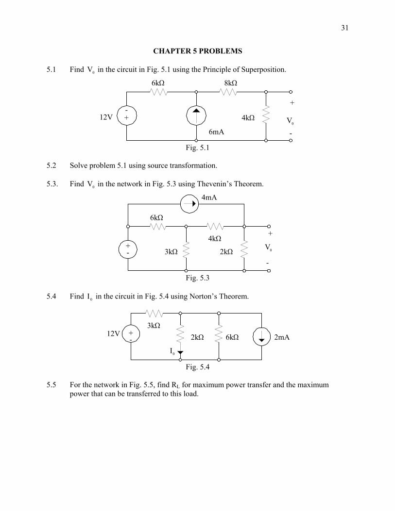
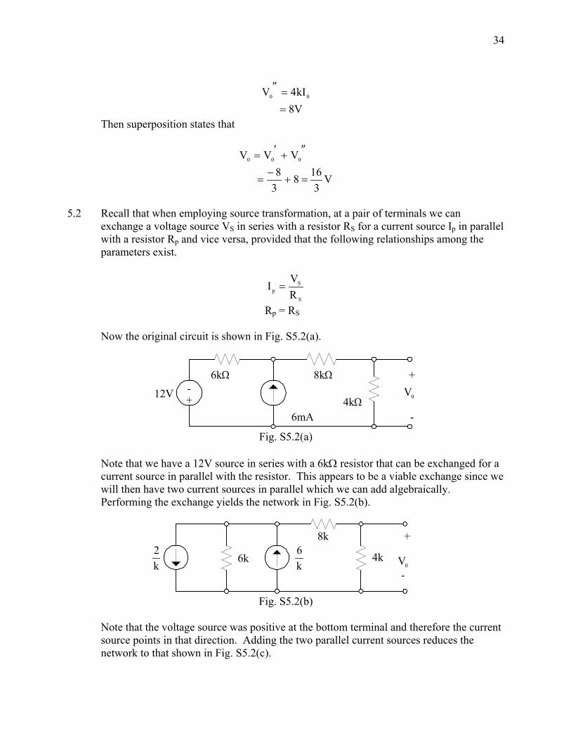
CHAPTER 5 PROBLEMS 5.1 Find 0V in the circuit in Fig. 5.1 using the Principle of Superposition.
+-
12V
6kΩ 8kΩ
6mA
4kΩ
+
-0V
Fig. 5.1
5.2 Solve problem 5.1 using source transformation. 5.3. Find 0V in the network in Fig. 5.3 using Thevenin’s Theorem.
6kΩ
2kΩ
4mA
4kΩ+
-
0V3kΩ+-
Fig. 5.3
5.4 Find 0I in the circuit in Fig. 5.4 using Norton’s Theorem.
+- 6kΩ2kΩ 2mA
3kΩ12V
0I
Fig. 5.4 5.5 For the network in Fig. 5.5, find RL for maximum power transfer and the maximum
power that can be transferred to this load.
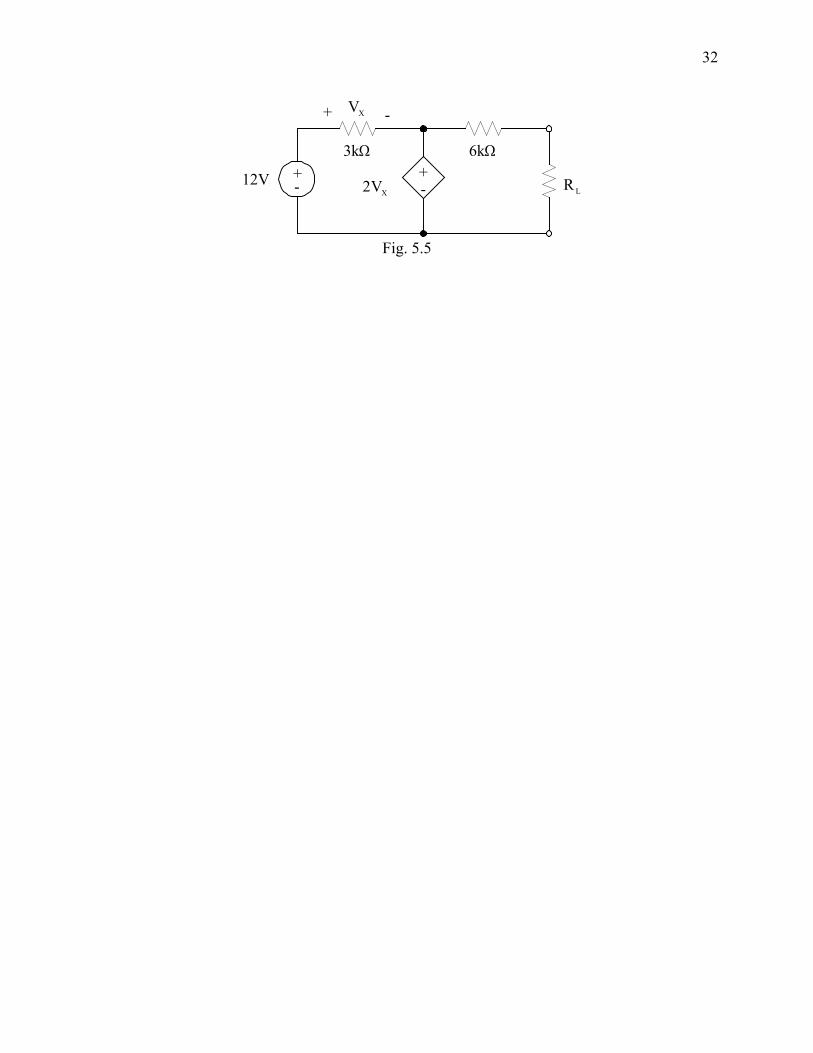
32
+-12V
3kΩ 6kΩ
+ -
+-XV2
XV
LR
Fig. 5.5
33
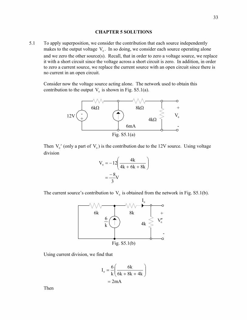
CHAPTER 5 SOLUTIONS 5.1 To apply superposition, we consider the contribution that each source independently
makes to the output voltage 0V . In so doing, we consider each source operating alone and we zero the other source(s). Recall, that in order to zero a voltage source, we replace it with a short circuit since the voltage across a short circuit is zero. In addition, in order to zero a current source, we replace the current source with an open circuit since there is no current in an open circuit.
Consider now the voltage source acting alone. The network used to obtain this
contribution to the output 0V is shown in Fig. S5.1(a).
+-12V
6kΩ 8kΩ
6mA4kΩ
+
-
0V
Fig. S5.1(a)
Then 0V ′ (only a part of 0V ) is the contribution due to the 12V source. Using voltage
division
V38
k8k6k4k412V0
−=
⎟⎟⎠
⎞⎜⎜⎝
⎛++
−=
The current source’s contribution to 0V is obtained from the network in Fig. S5.1(b).
6k 8k
4k
+
-
0V ′′k6
0I
Fig. S5.1(b)
Using current division, we find that
mA2k4k8k6
k6k6I0
=
⎟⎟⎠
⎞⎜⎜⎝
⎛++
=
Then
34
V8kI4V 00
==″
Then superposition states that
V3
16838
VVV 000
=+−
=
″+′=
5.2 Recall that when employing source transformation, at a pair of terminals we can
exchange a voltage source VS in series with a resistor RS for a current source Ip in parallel with a resistor Rp and vice versa, provided that the following relationships among the parameters exist.
S
Sp R
VI =
Rp = RS Now the original circuit is shown in Fig. S5.2(a).
+-12V
6kΩ 8kΩ
6mA4kΩ
+
-
0V
Fig. S5.2(a)
Note that we have a 12V source in series with a 6kΩ resistor that can be exchanged for a
current source in parallel with the resistor. This appears to be a viable exchange since we will then have two current sources in parallel which we can add algebraically. Performing the exchange yields the network in Fig. S5.2(b).
6k
8k
4k
+
-0Vk
6k2
Fig. S5.2(b)
Note that the voltage source was positive at the bottom terminal and therefore the current
source points in that direction. Adding the two parallel current sources reduces the network to that shown in Fig. S5.2(c).
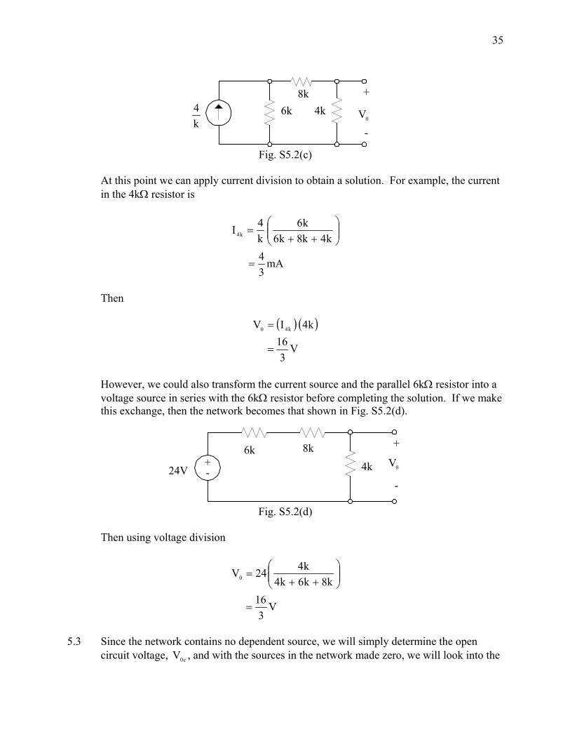
35
6k8k
4k
+
-0V
k4
Fig. S5.2(c)
At this point we can apply current division to obtain a solution. For example, the current
in the 4kΩ resistor is
mA34
k4k8k6k6
k4I k4
=
⎟⎟⎠
⎞⎜⎜⎝
⎛++
=
Then
( ) ( )
V3
16k4IV k40
=
=
However, we could also transform the current source and the parallel 6kΩ resistor into a
voltage source in series with the 6kΩ resistor before completing the solution. If we make this exchange, then the network becomes that shown in Fig. S5.2(d).
+-24V
6k 8k
4k
+
-
0V
Fig. S5.2(d)
Then using voltage division
V3
16k8k6k4
k424V0
=
⎟⎟⎠
⎞⎜⎜⎝
⎛++
=
5.3 Since the network contains no dependent source, we will simply determine the open
circuit voltage, c0V , and with the sources in the network made zero, we will look into the
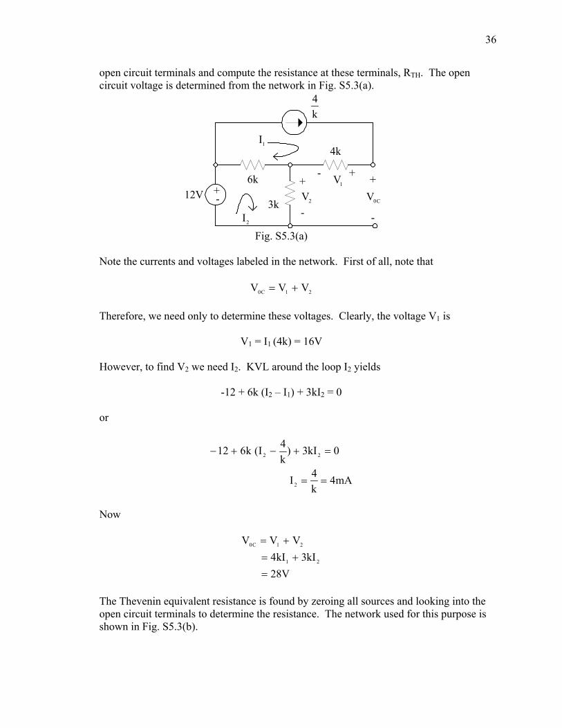
36
open circuit terminals and compute the resistance at these terminals, RTH. The open circuit voltage is determined from the network in Fig. S5.3(a).
12V +-
6k
4k
+
-
C0V3k
+
-2V
+-1V
1I
2I
k4
Fig. S5.3(a)
Note the currents and voltages labeled in the network. First of all, note that
21C0 VVV += Therefore, we need only to determine these voltages. Clearly, the voltage V1 is
V1 = I1 (4k) = 16V However, to find V2 we need I2. KVL around the loop I2 yields
-12 + 6k (I2 – I1) + 3kI2 = 0 or
mA4k4I
0kI3)k4I(k612
2
22
==
=+−+−
Now
V28kI3kI4
VVV
21
21C0
=+=
+=
The Thevenin equivalent resistance is found by zeroing all sources and looking into the
open circuit terminals to determine the resistance. The network used for this purpose is shown in Fig. S5.3(b).
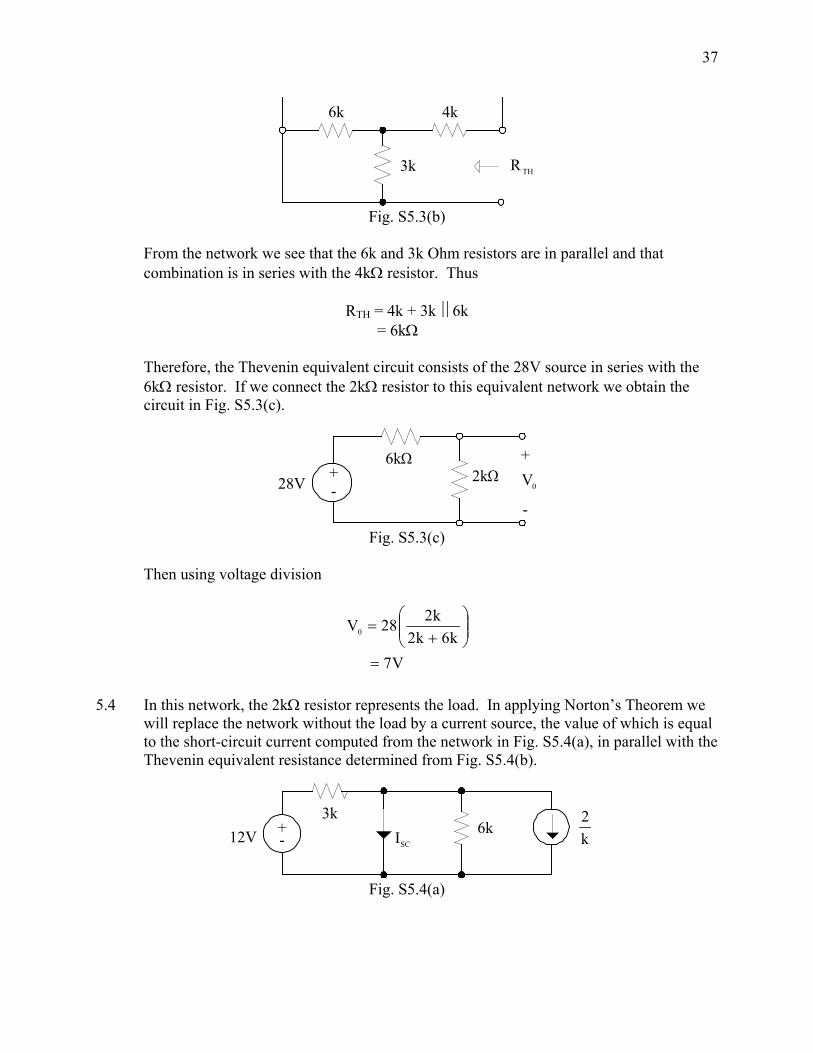
37
6k 4k
THR3k
Fig. S5.3(b)
From the network we see that the 6k and 3k Ohm resistors are in parallel and that
combination is in series with the 4kΩ resistor. Thus
RTH = 4k + 3k⎟ ⎜6k = 6kΩ Therefore, the Thevenin equivalent circuit consists of the 28V source in series with the
6kΩ resistor. If we connect the 2kΩ resistor to this equivalent network we obtain the circuit in Fig. S5.3(c).
6kΩ2kΩ
+
-0V28V
+-
Fig. S5.3(c)
Then using voltage division
V7k6k2
k228V0
=
⎟⎟⎠
⎞⎜⎜⎝
⎛+
=
5.4 In this network, the 2kΩ resistor represents the load. In applying Norton’s Theorem we
will replace the network without the load by a current source, the value of which is equal to the short-circuit current computed from the network in Fig. S5.4(a), in parallel with the Thevenin equivalent resistance determined from Fig. S5.4(b).
3k6k
SCI12V +- k
2
Fig. S5.4(a)
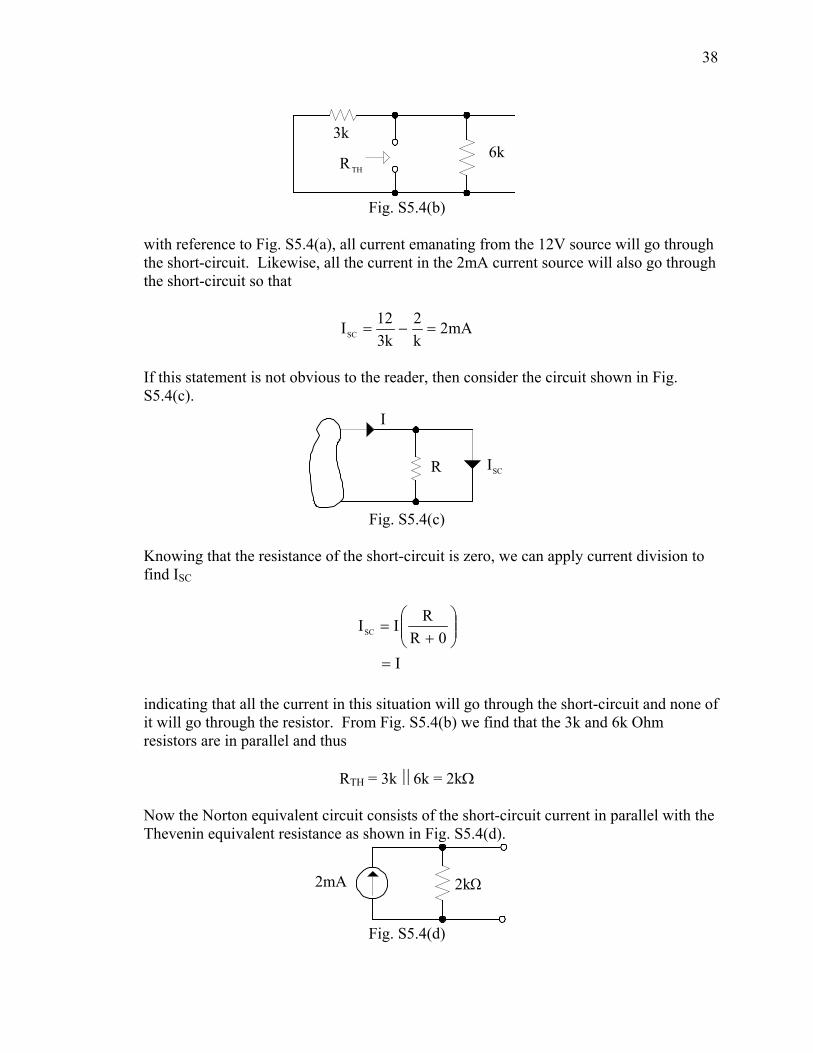
38
3k6k
THR
Fig. S5.4(b)
with reference to Fig. S5.4(a), all current emanating from the 12V source will go through
the short-circuit. Likewise, all the current in the 2mA current source will also go through the short-circuit so that
mA2k2
k312ISC =−=
If this statement is not obvious to the reader, then consider the circuit shown in Fig.
S5.4(c). I
R SCI
Fig. S5.4(c)
Knowing that the resistance of the short-circuit is zero, we can apply current division to
find ISC
I0R
RIISC
=
⎟⎟⎠
⎞⎜⎜⎝
⎛+
=
indicating that all the current in this situation will go through the short-circuit and none of
it will go through the resistor. From Fig. S5.4(b) we find that the 3k and 6k Ohm resistors are in parallel and thus
RTH = 3k⎟ ⎜6k = 2kΩ
Now the Norton equivalent circuit consists of the short-circuit current in parallel with the
Thevenin equivalent resistance as shown in Fig. S5.4(d).
2mA 2kΩ
Fig. S5.4(d)

39
Remember, at the terminals of the 2kΩ load, this network is equivalent to the original
network with the load removed. Therefore, if we now connect the load to the Norton equivalent circuit as shown in Fig. S5.4(e), the load current 0I can be calculated via current division as
mA1k2k2
k2k2I0
=
⎟⎟⎠
⎞⎜⎜⎝
⎛+
=
2k2kk2
0I Fig. S5.4(e)
5.5 The solution of this problem involves finding the Thevenin equivalent circuit at the
terminals of the load resistor RL and setting RL equal to the Thevenin equivalent resistance RTH.
To determine the Thevenin equivalent circuit, we first find the open circuit voltage as
shown in Fig. S5.5(a).
+-12
3k 6k
+ -
+- XV2 ′
XV′
C0V
+
-
Fig. S5.5(a) We employ the prime notation on the control variable Vx since the circuit in Fig. S5.5(a)
is different than the original network. Applying KVL to the left side of the network yields
-12 +Vx′ + 2Vx′ = 0
Vx′ = 4V Then the open circuit voltage is
V8V2V XC0
=
′=
since there is no current in the 6kΩ resistor and therefore no voltage drop across it.
40
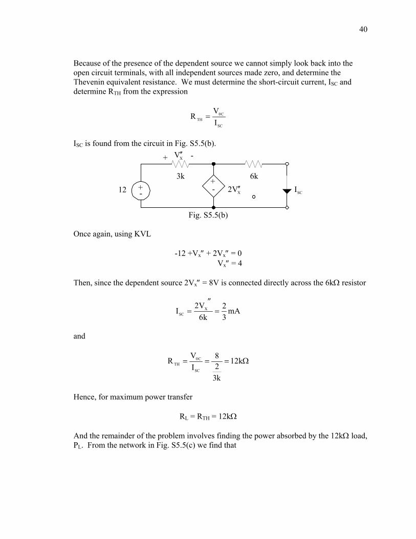
Because of the presence of the dependent source we cannot simply look back into the
open circuit terminals, with all independent sources made zero, and determine the Thevenin equivalent resistance. We must determine the short-circuit current, ISC and determine RTH from the expression
SC
C0TH I
VR =
ISC is found from the circuit in Fig. S5.5(b).
+-12
3k 6k
+ -
+- XV2 ′′
XV ′′
SCI
Fig. S5.5(b)
Once again, using KVL
-12 +Vx″ + 2Vx″ = 0 Vx″ = 4 Then, since the dependent source 2Vx″ = 8V is connected directly across the 6kΩ resistor
mA32
k6V2I X
SC =″
=
and
Ω=== k12
k328
IV
RSC
C0TH
Hence, for maximum power transfer
RL = RTH = 12kΩ And the remainder of the problem involves finding the power absorbed by the 12kΩ load,
PL. From the network in Fig. S5.5(c) we find that
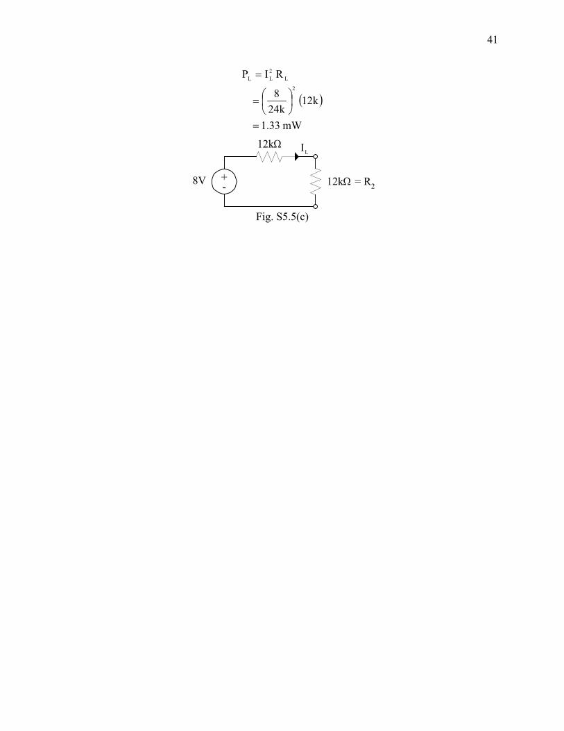
41
( )
mW33.1
k12k24
8
RIP2
L2LL
=
⎟⎠⎞
⎜⎝⎛=
=
+-
LI12kΩ
12kΩ = R28V
Fig. S5.5(c)
42
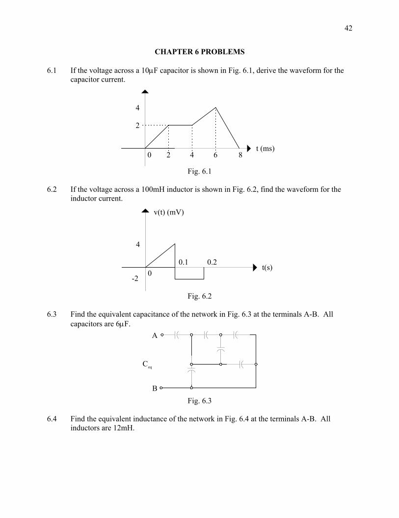
CHAPTER 6 PROBLEMS 6.1 If the voltage across a 10µF capacitor is shown in Fig. 6.1, derive the waveform for the
capacitor current.
4
2
4 6 80 2t (ms)
Fig. 6.1
6.2 If the voltage across a 100mH inductor is shown in Fig. 6.2, find the waveform for the
inductor current.
4
-2
0.2t(s)
00.1
v(t) (mV)
Fig. 6.2
6.3 Find the equivalent capacitance of the network in Fig. 6.3 at the terminals A-B. All
capacitors are 6µF. A
B
eqC
Fig. 6.3
6.4 Find the equivalent inductance of the network in Fig. 6.4 at the terminals A-B. All
inductors are 12mH.
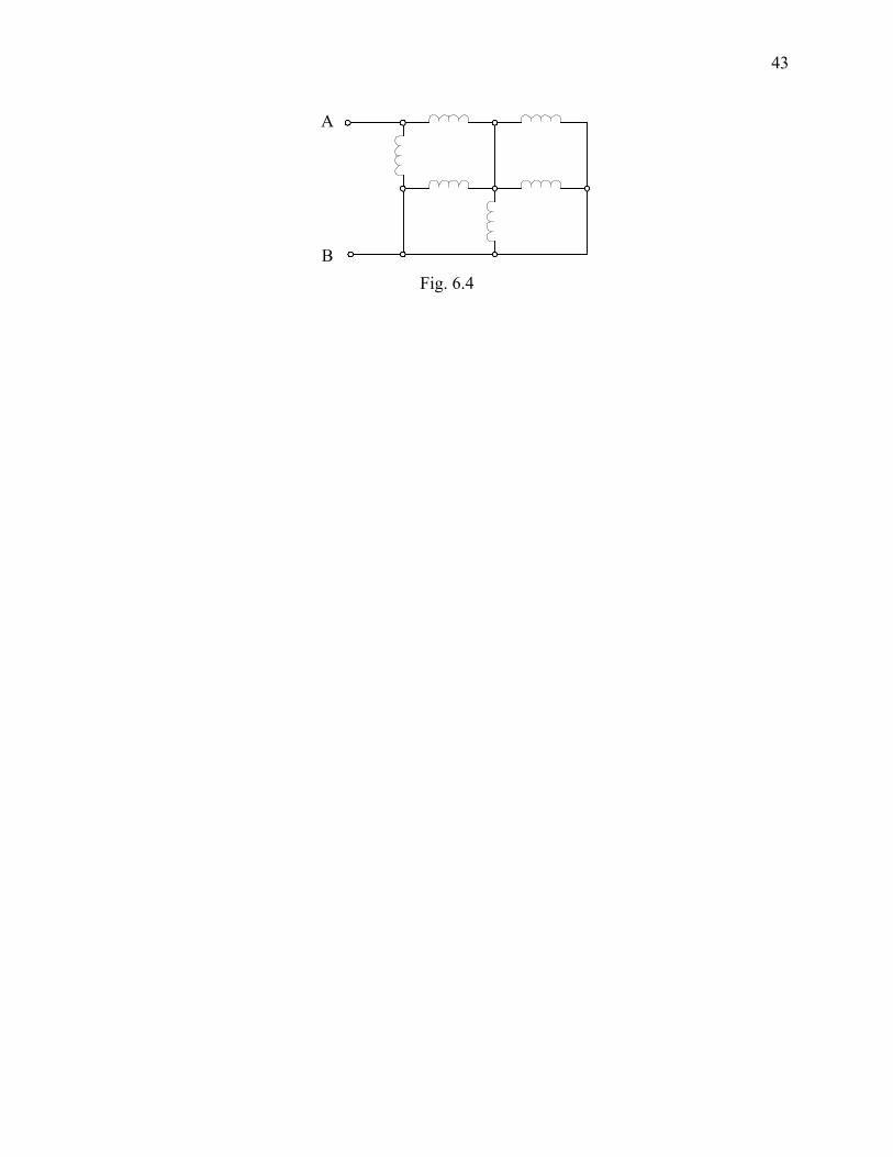
43
A
B Fig. 6.4
44
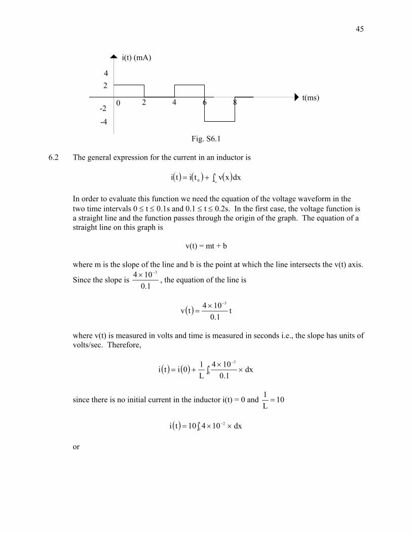
CHAPTER 6 SOLUTIONS 6.1 The equations for the waveforms in the 4 two millisecond time intervals are listed below.
( )
ms8t,0t0
ms8t6t102416
ms6t4t10222
ms4t22
ms2t0t1022
bmttv
3
3
3
><=
≤≤×
−+=
≤≤×
+−=
≤≤=
≤≤×
=
+=
−
−
−
Note that within each interval we have simply written the equation of a straight line using
the expression y = mx + b or equivalently v(t) = mt + b where m is the slope of the line and b is the point at which the line intersects the v(t) axis.
The equation for the current in a capacitor is
( )dt
tdvC)t(i =
Using this expression we can compute the current in each interval. For example, in the
interval from 0 ≤ t ≤ 2ms
( ) ( )
mA10
ms2t0t1022
dtd1010ti
36
=
≤≤⎟⎟⎠
⎞⎜⎜⎝
⎛×
×=−
−
( ) ( ) ( )
0
ms4t22dtd1010ti 6
=
≤≤×= −
( ) ( )
mA10
ms6t4t10222
dtd1010ti
36
=
≤≤⎟⎟⎠
⎞⎜⎜⎝
⎛×
+−×=−
−
( ) ( )
mA20
ms8t6t102416
dtd1010ti
36
−=
≤≤⎟⎟⎠
⎞⎜⎜⎝
⎛×
−×=−
−
The waveform for the capacitor current is shown in Fig. S6.1.
45
4
-24 t(ms)
0 2 6 8
-4
2
i(t) (mA)
Fig. S6.1
6.2 The general expression for the current in an inductor is
( ) ( ) ( )∫+= tt0 0
dxxvtiti In order to evaluate this function we need the equation of the voltage waveform in the
two time intervals 0 ≤ t ≤ 0.1s and 0.1 ≤ t ≤ 0.2s. In the first case, the voltage function is a straight line and the function passes through the origin of the graph. The equation of a straight line on this graph is
v(t) = mt + b
where m is the slope of the line and b is the point at which the line intersects the v(t) axis.
Since the slope is 1.0
104 3−× , the equation of the line is
( ) t1.0
104tv3−×
=
where v(t) is measured in volts and time is measured in seconds i.e., the slope has units of
volts/sec. Therefore,
( ) ( ) ∫ ××
+=−
t0
3
dx1.0
104L10iti
since there is no initial current in the inductor i(t) = 0 and 10L1
=
( ) ∫ ××= −t
02 dx10410ti
or
46
( )
mAt200At2.02
x4.0dx4.0ti
22
t0
t0
2
==
∫ =×=
Since the initial current for the second time interval is determined by the value of the
current at the end of the first time interval we calculate
( )mA2
mAt200ti 1.0t2
1.0t
=
= ==
Therefore, in the time interval 0.1 ≤ t ≤ 0.2s
( ) ( ) ( )∫+= t1.0 dxxv
L11.0iti
Note that in this interval v(x) is a constant –2mV or –2 × 10⁻³V. Hence,
( ) ( )
( )mAt204
1020102
dx10210102tit
1.033
t1.0
33
−=
××−×=
∫ ×−+×=−−
−−
If we now plot the two functions for the current within their respective time intervals we
obtain the plot in Fig. S6.2.
2
0.2t(s)
0 0.1
Fig. S6.2 6.3 To begin our analysis we first label all the capacitors and nodes in the network as shown
in Fig. S6.3(a).
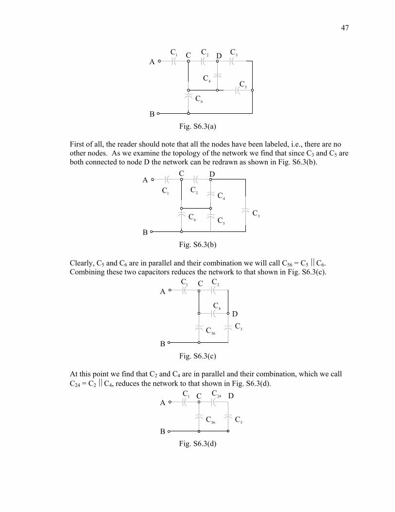
47
A
B
1C 2C 3C
4C5C
6C
C D
Fig. S6.3(a)
First of all, the reader should note that all the nodes have been labeled, i.e., there are no
other nodes. As we examine the topology of the network we find that since C3 and C5 are both connected to node D the network can be redrawn as shown in Fig. S6.3(b).
A
B
1C 2C
3C
4C
5C6C
C D
Fig. S6.3(b)
Clearly, C5 and C6 are in parallel and their combination we will call C56 = C5⎟ ⎜C6.
Combining these two capacitors reduces the network to that shown in Fig. S6.3(c).
A
B
1C 2C
3C
4C
56C
C
D
Fig. S6.3(c)
At this point we find that C2 and C4 are in parallel and their combination, which we call
C24 = C2⎟ ⎜C4, reduces the network to that shown in Fig. S6.3(d).
A
B
1C 24C
3C56C
C D
Fig. S6.3(d)
48
If we now use the given capacitor values, the network becomes that shown in Fig. S6.3(e).
A
B
6µF
6µF
12µF
12µF
Fig. S6.3(e)
Starting at the opposite end of the network from the terminals A-B and combining
elements we find that 6µF in series with 12µF is 4µF and this equivalent capacitance is in parallel with 12µF yielding 16µF, which in turn is in series with 6µF producing a total capacitance of
F36.4F16F6Ceq
µ=
µµ=
6.4 To aid our analysis, we will first label all inductors and nodes as shown in Fig. S6.4(a).
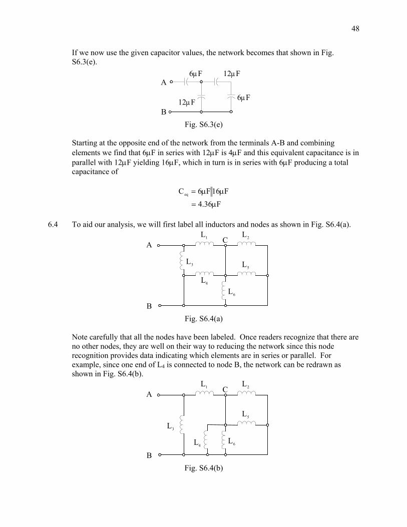
A
B
1L 2L
3L
4L
5L
6L
C
Fig. S6.4(a)
Note carefully that all the nodes have been labeled. Once readers recognize that there are
no other nodes, they are well on their way to reducing the network since this node recognition provides data indicating which elements are in series or parallel. For example, since one end of L4 is connected to node B, the network can be redrawn as shown in Fig. S6.4(b).
A
B
1L 2L
3L
4L
5L
6L
C
Fig. S6.4(b)
49
This diagram clearly indicates that L2 and L5 are in parallel. In addition, L4 and L6 are in
parallel. Therefore, if we combine elements so that L25 = L2⎟ ⎜L5 and L46 = L4⎟ ⎜L6, then the circuit can be reduced to that in Fig. S6.4(c).
A
B
1L 25L
3L 46L
C
Fig. S6.4(c)
However, we note now if we did not see it earlier that L25 is in parallel with L46 so that
the network can be reduced to that shown in Fig. S6.4(d).
A
B
1L
2456L3L
C
Fig. S6.4(d)
Where L2456 = L25⎟ ⎜L46. Since all inductors are 12mH, L2456 = 3mH which is in series
with 12mH and that combination is in parallel with 12mH yielding
LAB = 12mH⎟ ⎜15mH = 6.66mH
50
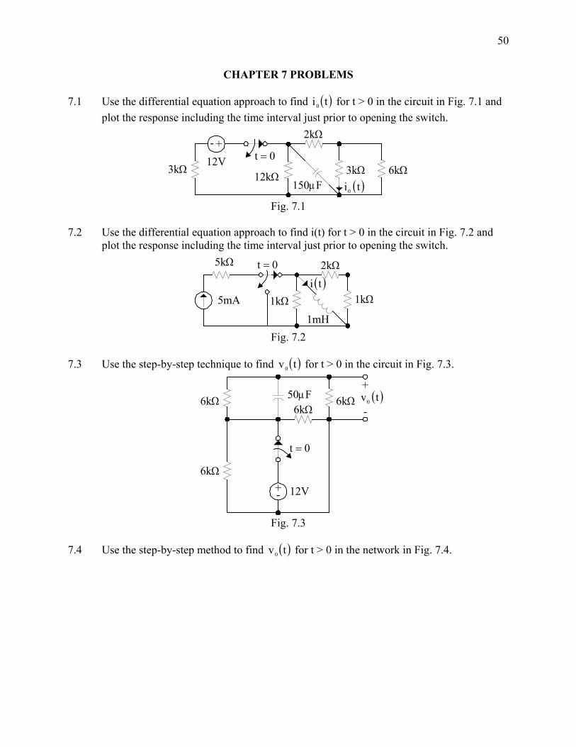
CHAPTER 7 PROBLEMS 7.1 Use the differential equation approach to find ( )ti 0 for t > 0 in the circuit in Fig. 7.1 and
plot the response including the time interval just prior to opening the switch.
+-
12V3kΩ
12kΩ
2kΩ
3kΩ 6kΩ0t =
( )ti0150µF
Fig. 7.1
7.2 Use the differential equation approach to find i(t) for t > 0 in the circuit in Fig. 7.2 and
plot the response including the time interval just prior to opening the switch.
5mA 1kΩ
2kΩ
1kΩ
1mH
0t =
( )ti
5kΩ
Fig. 7.2
7.3 Use the step-by-step technique to find ( )tv0 for t > 0 in the circuit in Fig. 7.3.
50µF6kΩ
6kΩ
12V
0t =
( )tv06kΩ
6kΩ
+
-
+-
Fig. 7.3 7.4 Use the step-by-step method to find ( )tv0 for t > 0 in the network in Fig. 7.4.

51
4Ω
12V
0t =
( )tv0
2Ω
12V
+
-+-
+- 2Ω
H31
Fig. 7.4
7.5 Given the network in Fig. 7.5, find (a) the differential equation that describes the current i(t) (b) the characteristic equation for the network (c) the network’s natural frequencies (d) the type of damping exhibited by the circuit (e) the general expression for i(t)
( )ti
( )tvS 14Ω
2H
0.05F
+-
Fig. 7.5
7.6 Find ( )ti 0 for t > 0 in the circuit in Fig. 7.6 and plot the response including the time
interval just prior to closing the switch.
12V
0t = 24Ω
F120
1
24Ω 24Ω2.4H
( )ti0
+-
Fig. 7.6
52
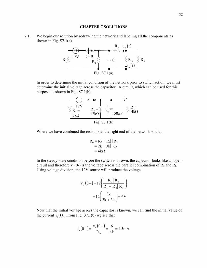
CHAPTER 7 SOLUTIONS 7.1 We begin our solution by redrawing the network and labeling all the components as
shown in Fig. S7.1(a)
+-
12VC
0t =
( )ti0
( )tiX
5R1R2R 4R
3R
Fig. S7.1(a)
In order to determine the initial condition of the network prior to switch action, we must
determine the initial voltage across the capacitor. A circuit, which can be used for this purpose, is shown in Fig. S7.1(b).
+-12V
Xi
Cv150µF
=1R3kΩ
=2R12kΩ
=6R4kΩ
+
-
Fig. S7.1(b) Where we have combined the resistors at the right end of the network so that
R6 = R3 + R4⎥⎜R5 = 2k + 3k⎥⎜6k = 4kΩ In the steady-state condition before the switch is thrown, the capacitor looks like an open-
circuit and therefore vC(0-) is the voltage across the parallel combination of R2 and R6. Using voltage division, the 12V source will produce the voltage
( )
V6k3k3
k312
RRRRR
120v621
62C
=⎟⎟⎠
⎞⎜⎜⎝
⎛+
=
⎟⎟⎠
⎞⎜⎜⎝
⎛
+=−
Now that the initial voltage across the capacitor is known, we can find the initial value of
the current ( )ti 0 . From Fig. S7.1(b) we see that
( ) ( )mA5.1
k46
R0v
0i6
Cx ==
−=−
53
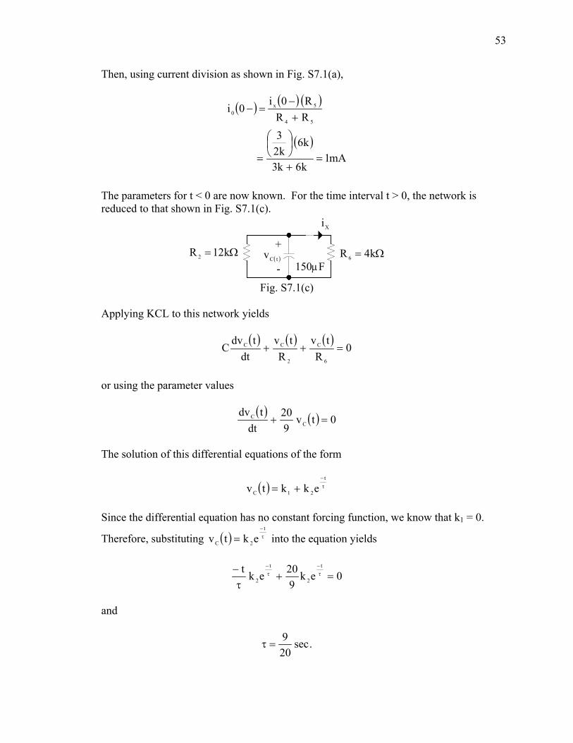
Then, using current division as shown in Fig. S7.1(a),
( ) ( ) ( )
( )mA1
k6k3
k6k23
RRR0i
0i54
5x0
=+
⎟⎠⎞
⎜⎝⎛
=
+−
=−
The parameters for t < 0 are now known. For the time interval t > 0, the network is
reduced to that shown in Fig. S7.1(c). Xi
Ω= k4R 6( )tCvΩ= k12R 2
+
- 150µF
Fig. S7.1(c) Applying KCL to this network yields
( ) ( ) ( )0
Rtv
Rtv
dttdv
C6
C
2
CC =++
or using the parameter values
( ) ( ) 0tv920
dttdv
CC =+
The solution of this differential equations of the form
( ) τ−
+=t
21C ekktv Since the differential equation has no constant forcing function, we know that k1 = 0.
Therefore, substituting ( ) τ−
=t
2C ektv into the equation yields
0ek920ekt t
2
t
2 =+τ
− τ−
τ−
and
.sec209
=τ
54
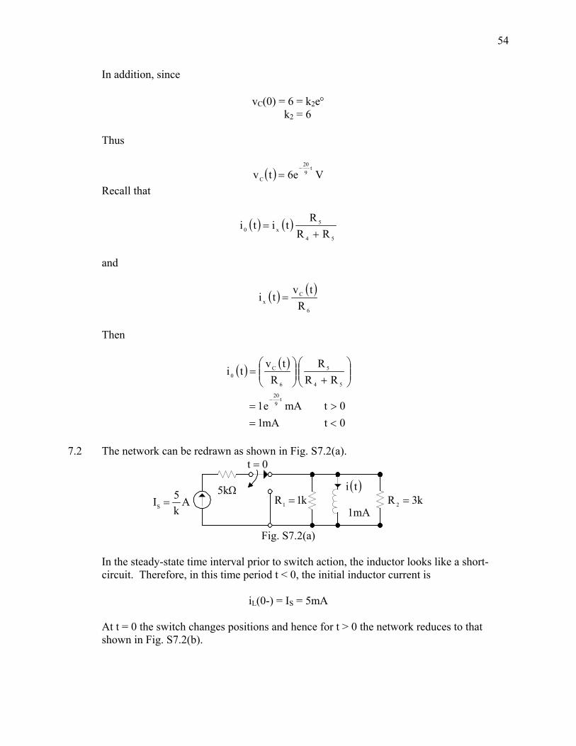
In addition, since
vC(0) = 6 = k2e° k2 = 6 Thus
( ) Ve6tvt
920
C
−=
Recall that
( ) ( )54
5x0 RR
Rtiti
+=
and
( ) ( )6
Cx R
tvti =
Then
( ) ( )
0tmA10tmAe1
RRR
Rtv
ti
t920
54
5
6
C0
<=>=
⎟⎟⎠
⎞⎜⎜⎝
⎛+⎟⎟
⎠
⎞⎜⎜⎝
⎛=
−
7.2 The network can be redrawn as shown in Fig. S7.2(a).
1mA
0t =
( )ti5kΩk1R1 = k3R 2 =A
k5IS =
Fig. S7.2(a)
In the steady-state time interval prior to switch action, the inductor looks like a short-
circuit. Therefore, in this time period t < 0, the initial inductor current is
iL(0-) = IS = 5mA At t = 0 the switch changes positions and hence for t > 0 the network reduces to that
shown in Fig. S7.2(b).
55
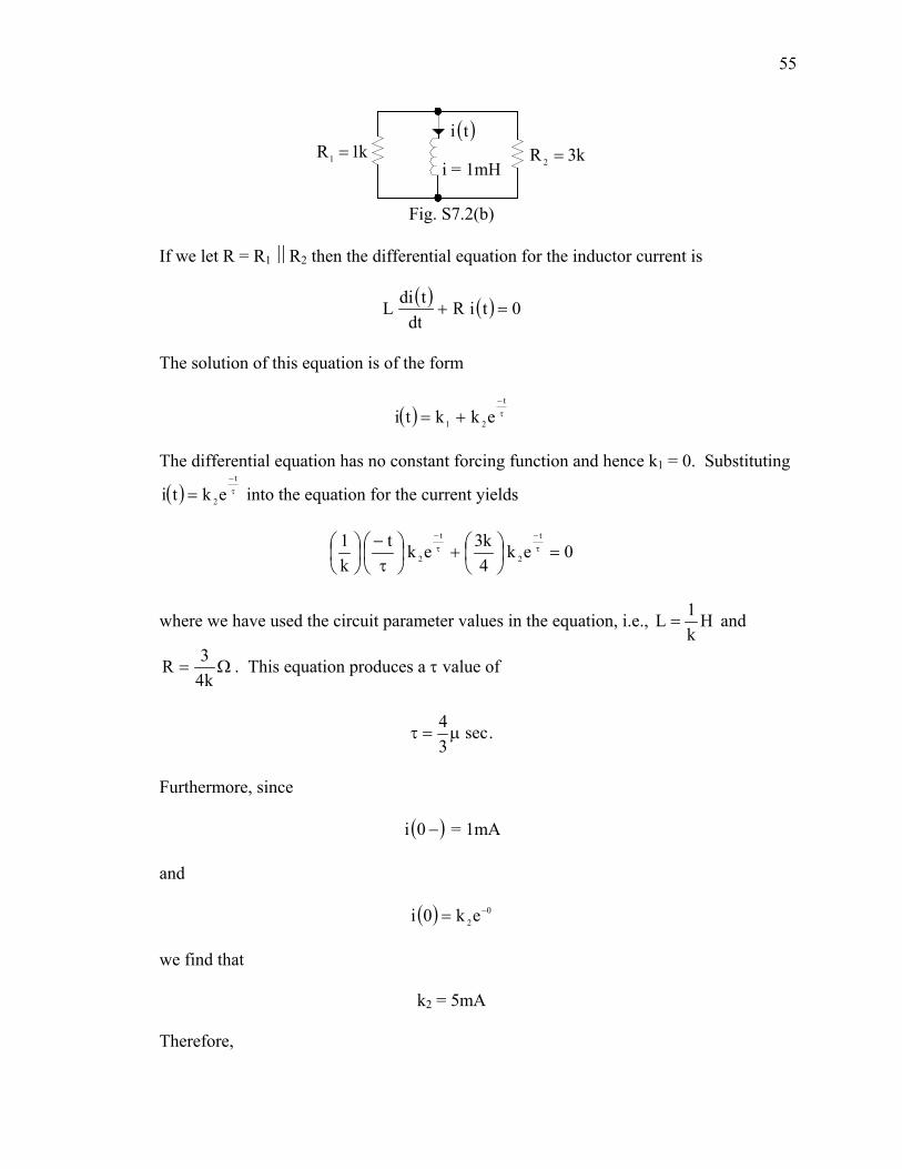
i = 1mH
( )tik3R 2 =k1R1 =
Fig. S7.2(b)
If we let R = R1⎟ ⎜R2 then the differential equation for the inductor current is
( ) ( ) 0tiRdt
tdiL =+
The solution of this equation is of the form
( ) τ−
+=t
21 ekkti The differential equation has no constant forcing function and hence k1 = 0. Substituting
( ) τ−
=t
2ekti into the equation for the current yields
0ek4k3ekt
k1 t
2
t
2 =⎟⎠⎞
⎜⎝⎛+⎟
⎠⎞
⎜⎝⎛
τ−
⎟⎠⎞
⎜⎝⎛ τ
−τ
−
where we have used the circuit parameter values in the equation, i.e., Hk1L = and
Ω=k43R . This equation produces a τ value of
.sec34
µ=τ
Furthermore, since
( )−0i = 1mA and
( ) 02ek0i −=
we find that
k2 = 5mA Therefore,
56
( )
0t,mAe5
0t,mA5tit105.7 5
>=
<=×−
7.3 The circuit is redrawn for convenience in Fig. S7.3(a).
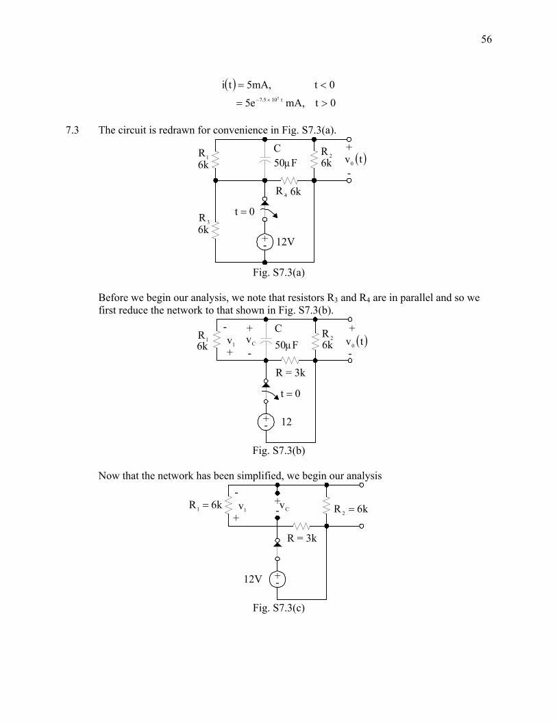
50µF
6k
6k
12V
0t =
( )tv0
+
-
6k
6k2R
1R
3R
4R
C
+-
Fig. S7.3(a) Before we begin our analysis, we note that resistors R3 and R4 are in parallel and so we
first reduce the network to that shown in Fig. S7.3(b).
50µF
R = 3k
6k
12
0t =
( )tv0
+
-
+-
2R1R C
1v+
-Cv
+
-6k
Fig. S7.3(b)
Now that the network has been simplified, we begin our analysis
R = 3k
12V +-
k6R 2 =k6R1 =1v
+
-Cv+
-
Fig. S7.3(c)
57
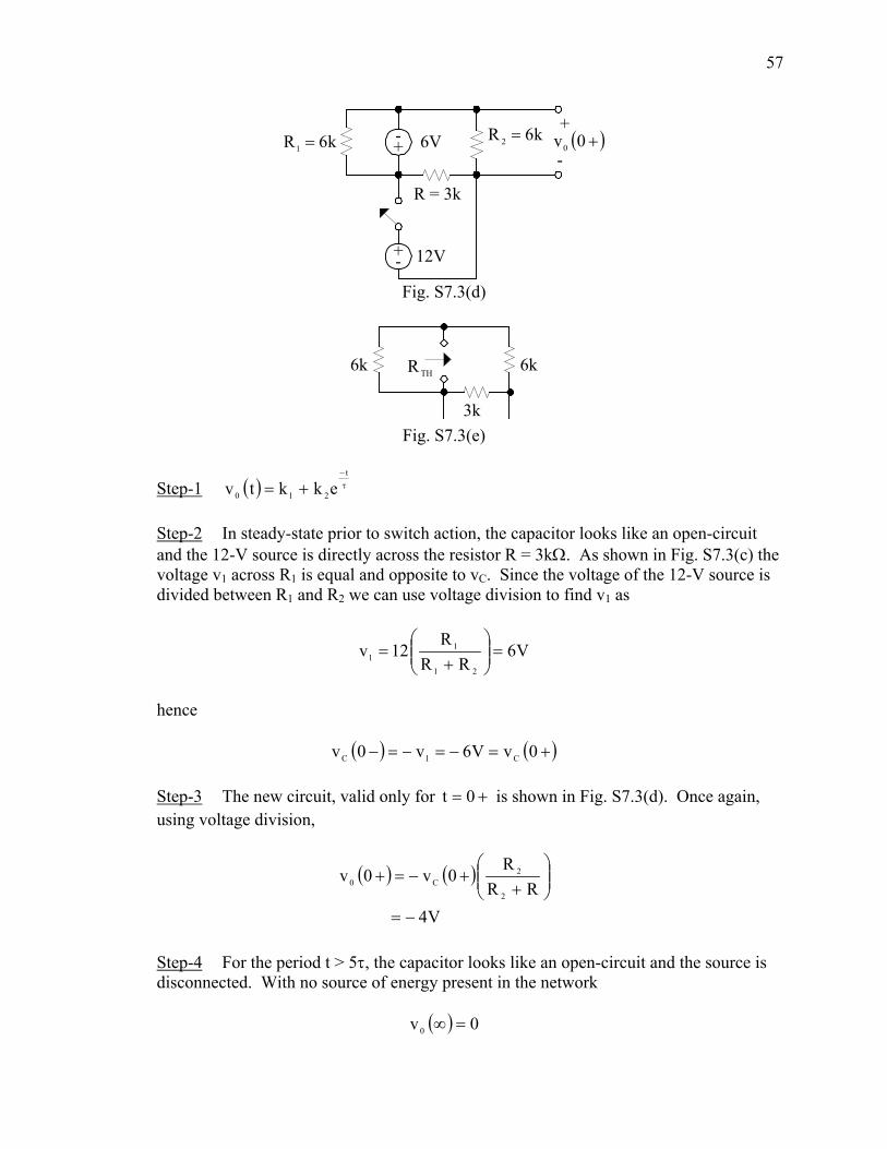
R = 3k
12V
( )+0v0
+
-k6R 2 =k6R1 = 6V+
-
+-
Fig. S7.3(d)
THR6k 6k
3k Fig. S7.3(e)
Step-1 ( ) τ−
+=t
210 ekktv Step-2 In steady-state prior to switch action, the capacitor looks like an open-circuit
and the 12-V source is directly across the resistor R = 3kΩ. As shown in Fig. S7.3(c) the voltage v1 across R1 is equal and opposite to vC. Since the voltage of the 12-V source is divided between R1 and R2 we can use voltage division to find v1 as
V6RR
R12v
21
11 =⎟⎟
⎠
⎞⎜⎜⎝
⎛+
=
hence
( ) ( )+=−=−=− 0vV6v0v C1C Step-3 The new circuit, valid only for += 0t is shown in Fig. S7.3(d). Once again,
using voltage division,
( ) ( )
V4RR
R0v0v
2
2C0
−=
⎟⎟⎠
⎞⎜⎜⎝
⎛+
+−=+
Step-4 For the period t > 5τ, the capacitor looks like an open-circuit and the source is
disconnected. With no source of energy present in the network
( ) 0v0 =∞
58
Step-5 The Thevenin equivalent resistance obtained by looking into the network from
the terminals of the capacitor with all sources made zero is derived from the circuit in Fig. S7.3(e)
RTH = (6k)⎟ ⎜(6k + 3k)
= 3.6kΩ Then the time constant of the network is
τ = RTHC = 0.18 sec. Step-6 Evaluating the constants in the solution, we find that ( ) 0vk 01 =∞=
( ) ( ) 4v0vk 002 −=∞−+= Therefore,
( ) Ve4tv 18.0t
0
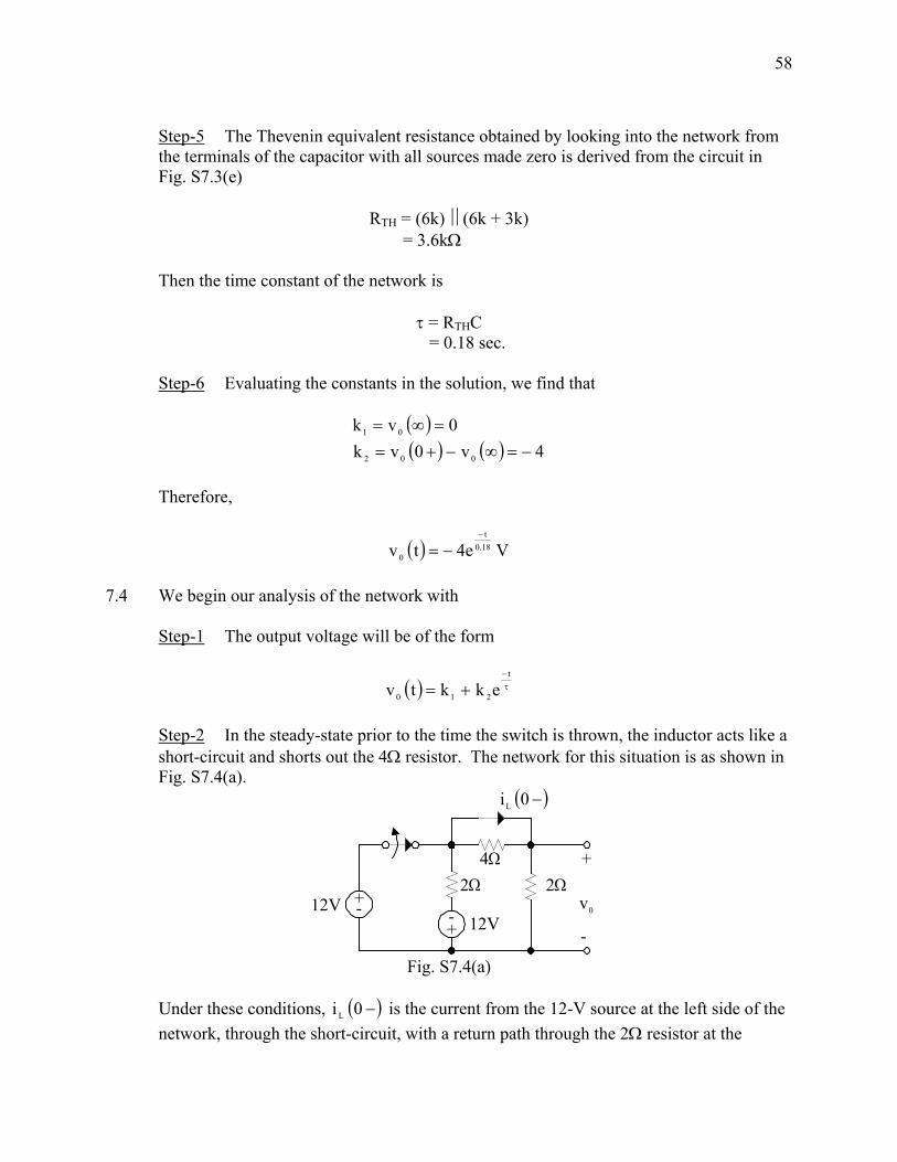
−
−= 7.4 We begin our analysis of the network with Step-1 The output voltage will be of the form
( ) τ−
+=t
210 ekktv Step-2 In the steady-state prior to the time the switch is thrown, the inductor acts like a
short-circuit and shorts out the 4Ω resistor. The network for this situation is as shown in Fig. S7.4(a).
0v12V2Ω
12V
2Ω4Ω
+
+- -
+
-
( )−0iL
Fig. S7.4(a)
Under these conditions, ( )−0iL is the current from the 12-V source at the left side of the
network, through the short-circuit, with a return path through the 2Ω resistor at the
59
output. What is the contribution of the 12V source in the center of the network? No contribution! Why? If we applied superposition and treated each source independently, we would quickly find that when the left-most source was replaced with a short-circuit, all the current from the other 12-V source would be diverted through this short-circuit. Therefore,
( ) ( )+===− 0iA62
120i LL
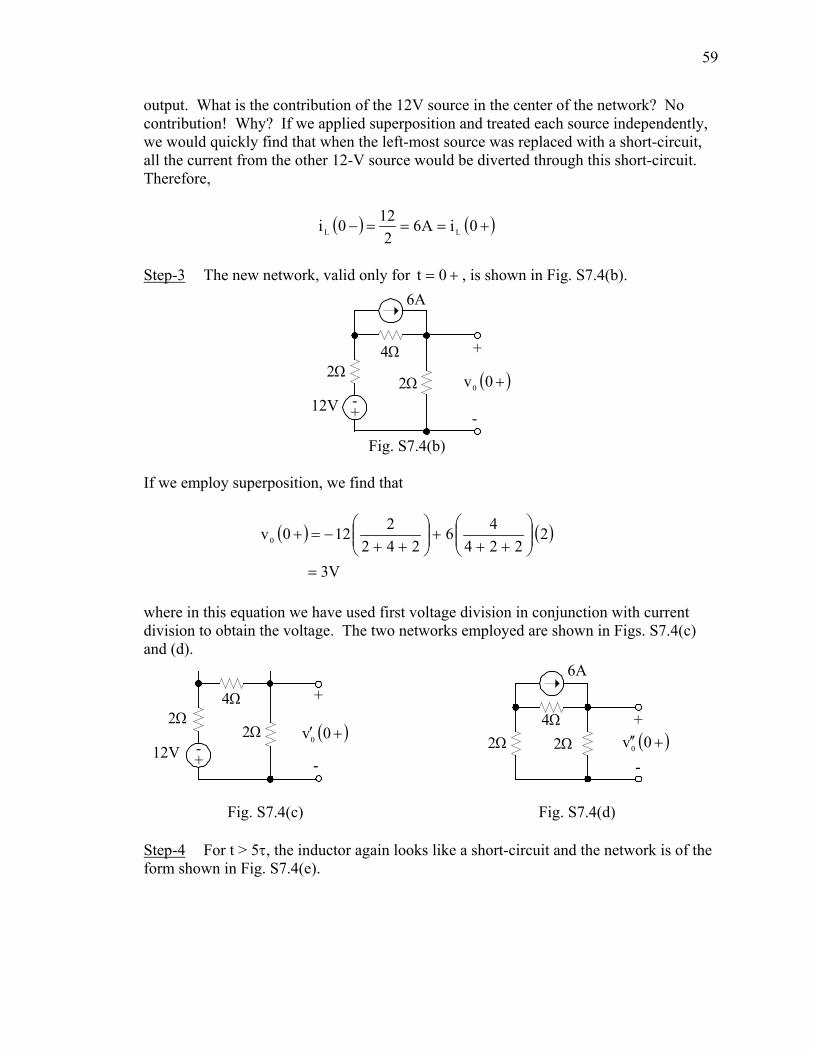
Step-3 The new network, valid only for += 0t , is shown in Fig. S7.4(b).
( )+0v0
6A
2Ω12V
2Ω4Ω
+-
+
-
Fig. S7.4(b) If we employ superposition, we find that
( ) ( )
V3
2224
46242
2120v0
=
⎟⎟⎠
⎞⎜⎜⎝
⎛++
+⎟⎟⎠
⎞⎜⎜⎝
⎛++
−=+
where in this equation we have used first voltage division in conjunction with current
division to obtain the voltage. The two networks employed are shown in Figs. S7.4(c) and (d).
( )+′ 0v02Ω
12V
2Ω4Ω
+-
+
-
( )+′′ 0v0
6A
2Ω2Ω4Ω +
-
Fig. S7.4(c) Fig. S7.4(d) Step-4 For t > 5τ, the inductor again looks like a short-circuit and the network is of the
form shown in Fig. S7.4(e).
60
( )∞0v2Ω12V
2Ω4Ω
+-
+
-
Fig. S7.4(e) A simple voltage divider indicates that the output voltage is
( ) V622
212v0 −=⎟⎟⎠
⎞⎜⎜⎝
⎛+
−=∞
Step-5 The Thevenin equivalent resistance obtained by looking into the circuit from the
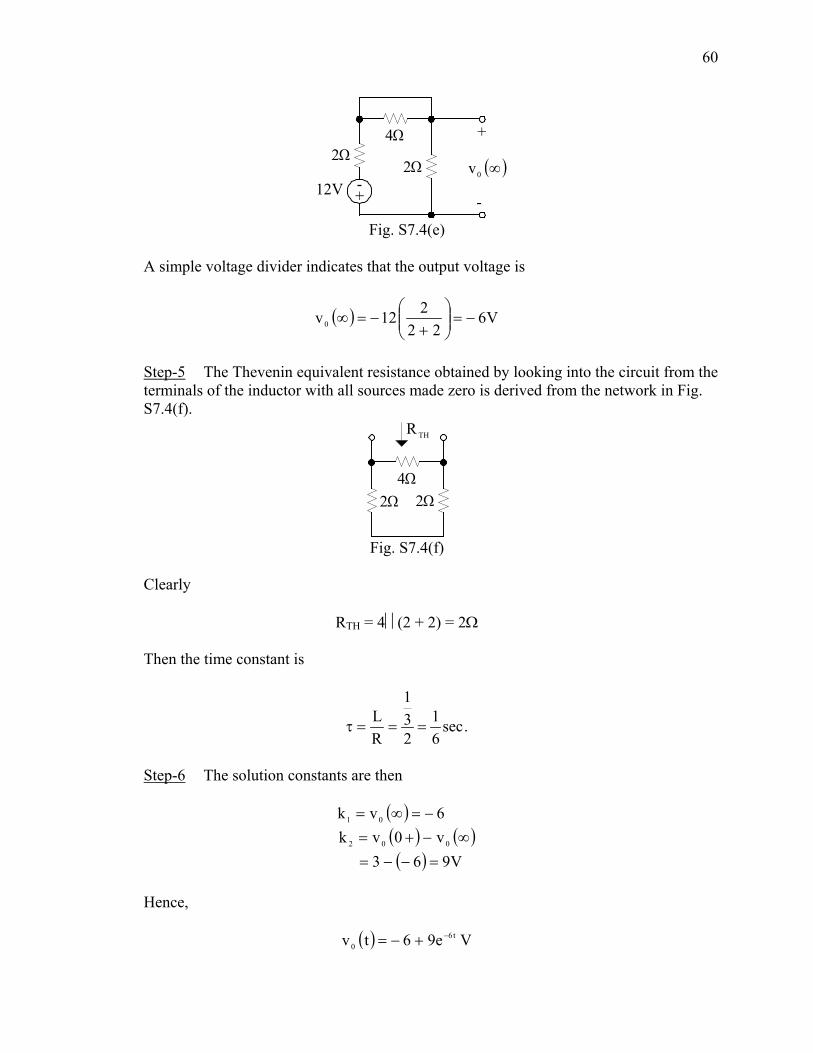
terminals of the inductor with all sources made zero is derived from the network in Fig. S7.4(f).
2Ω
THR
2Ω4Ω
Fig. S7.4(f)
Clearly
RTH = 4⎥⎜(2 + 2) = 2Ω Then the time constant is
.sec61
231
RL
===τ
Step-6 The solution constants are then ( ) 6vk 01 −=∞=
( ) ( )( ) V963
v0vk 002
=−−=∞−+=
Hence,
( ) Ve96tv t60
−+−=
61
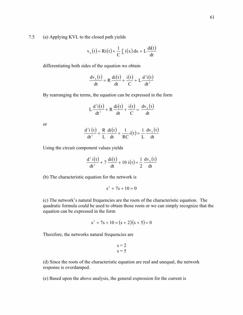
7.5 (a) Applying KVL to the closed path yields
( ) ( ) ( ) ( )dt
tdiLdxxiC1tRitv t
tS 0+∫+=
differentiating both sides of the equation we obtain
( ) ( ) ( ) ( )2
2S
dttidL
Cti
dttdiR
dttdv
++=
By rearranging the terms, the equation can be expressed in the form
( ) ( ) ( ) ( )dt
tdvCti
dttdiR
dttidL S
2
2
=++
or
( ) ( ) ( ) ( )dt
tdvL1ti
RC1
dttdi
LR
dttid S
2
2
=++
Using the circuit component values yields
( ) ( ) ( ) ( )dt
tdv21ti10
dttdi7
dttid S
2
2
=++
(b) The characteristic equation for the network is
010s7s2 =++ (c) The network’s natural frequencies are the roots of the characteristic equation. The
quadratic formula could be used to obtain those roots or we can simply recognize that the equation can be expressed in the form
( ) ( ) 05s2s10s7s2 =++=++
Therefore, the networks natural frequencies are
s = 2 s = 5
(d) Since the roots of the characteristic equation are real and unequal, the network
response is overdamped. (e) Based upon the above analysis, the general expression for the current is
62
( ) Aekekkti t5
2t2
10−− ++=
where 0k is the steady-state value and the constants k1 and k2 are determined from initial
conditions. 7.6 The network is re-labeled as shown in Fig. S7.6(a).
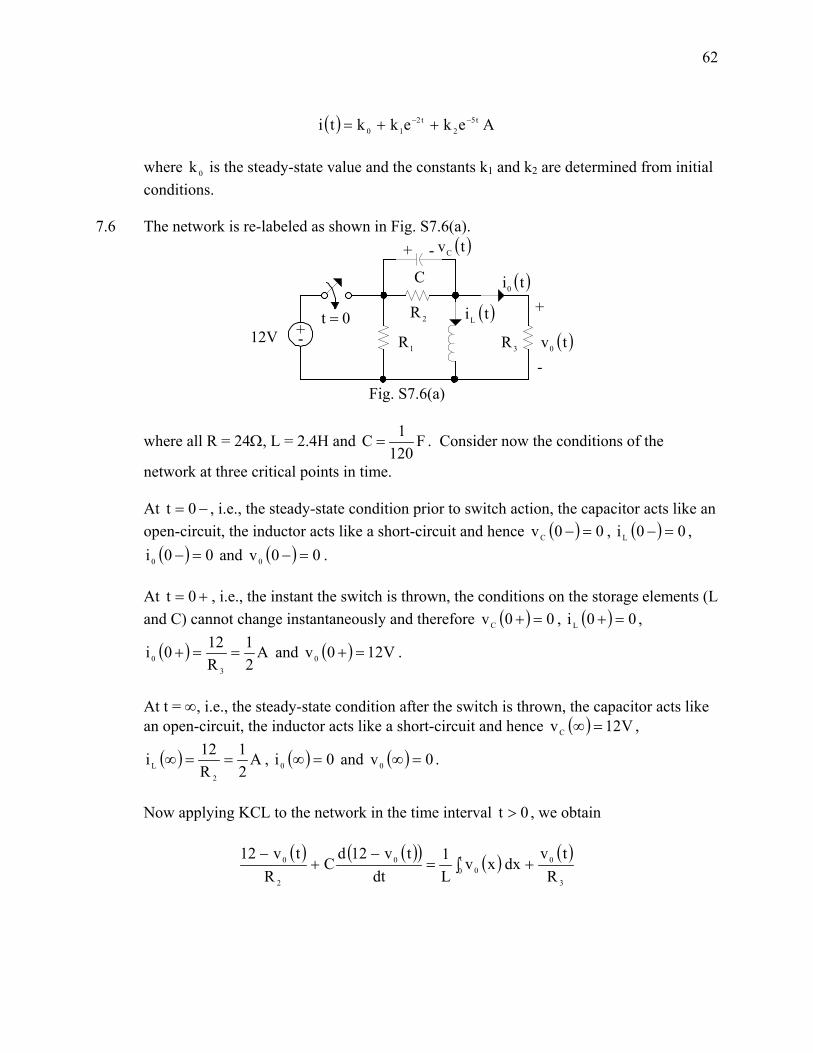
12V0t =
C
( )tvC
+( )ti0
+-
+ -
1R2R
3R-
( )tiL
( )tv0
Fig. S7.6(a)
where all R = 24Ω, L = 2.4H and F120
1C = . Consider now the conditions of the
network at three critical points in time. At −= 0t , i.e., the steady-state condition prior to switch action, the capacitor acts like an
open-circuit, the inductor acts like a short-circuit and hence ( ) 00vC =− , ( ) 00iL =− , ( ) 00i0 =− and ( ) 00v0 =− .
At += 0t , i.e., the instant the switch is thrown, the conditions on the storage elements (L
and C) cannot change instantaneously and therefore ( ) 00vC =+ , ( ) 00iL =+ ,
( ) A21
R120i
30 ==+ and ( ) V120v0 =+ .
At t = ∞, i.e., the steady-state condition after the switch is thrown, the capacitor acts like
an open-circuit, the inductor acts like a short-circuit and hence ( ) V12vC =∞ ,
( ) A21
R12i
2L ==∞ , ( ) 0i0 =∞ and ( ) 0v0 =∞ .
Now applying KCL to the network in the time interval 0t > , we obtain
( ) ( )( ) ( ) ( )3
0t0 0
0
2
0
Rtv
dxxvL1
dttv12d
CR
tv12+∫=
−+
−
63
where ( ) ( )3
00 R
tvti = expressing ( )tv0 in terms of ( )ti 0 and using the component values
reduces the equation to
( ) ( ) ( ) ( ) 0tidxxi10dt
tdi51ti
21
0t0 0
00 =−∫−−−
Combining terms and differentiating this expression yields
( ) ( ) ( ) 0ti50dt
tdi10
dttid
00
20
2
=++
Therefore, the characteristic equation for the network is
s2 + 10s + 50 = 0 Factoring this equation using the quadratic formula or any other convenient means yields
s1, s2 = -5 ± j5 = σ ± jω Since the roots of the characteristic equation are complex conjugates, the network is
underdamped and the general form of the current ( )ti 0 is
( ) ( )( )t5sinBt5cosAek
tsinBtcosAektit5
t0
++=
ω+ω+=−
σ−
where k is the steady-state term resulting from the presence of the voltage source in the
time interval t → ∞. We can now evaluate the constants k, A and B using the known conditions for the
network. For example,
( ) Ak210i0 +==+
and
( ) k0i0 ==∞
Therefore, 0k = and 21A = .
64
We need another equation in order to evaluate the constant B. If we return to our original equation and evaluate it at time += 0t , we have
( )
30t
0
2 R120
dttdv
1201
R1212
+=⎟⎠⎞
⎜⎝⎛ −
+−
+=
where ( ) V120v0 =+ , the integration interval is zero and the derivative function is our
unknown. Therefore,
( )60
dttdv
0t0 −=+=
or
( )5.2
dttdi
0t0 −=+=
The general form of the solution is
( ) ⎟⎠⎞
⎜⎝⎛ += − t5sinBt5cos
21eti t5
0
Then
( )t5cosB5et5sinBe5t5sin
25et5cos
21e5
dttdi t5t5t5t50 −−−− +−⎟
⎠⎞
⎜⎝⎛ −
+⎟⎠⎞
⎜⎝⎛−=
and
( )B5
25
dttdi
0t0 +
−=+=
Therefore,
B5255.2 +
−=−
or
0B = The general solution is then
65
( )
0tt5cose21
0t0ti
t5
0
>=
<=
−
A plot of this function is shown in Fig. S7.6(b).
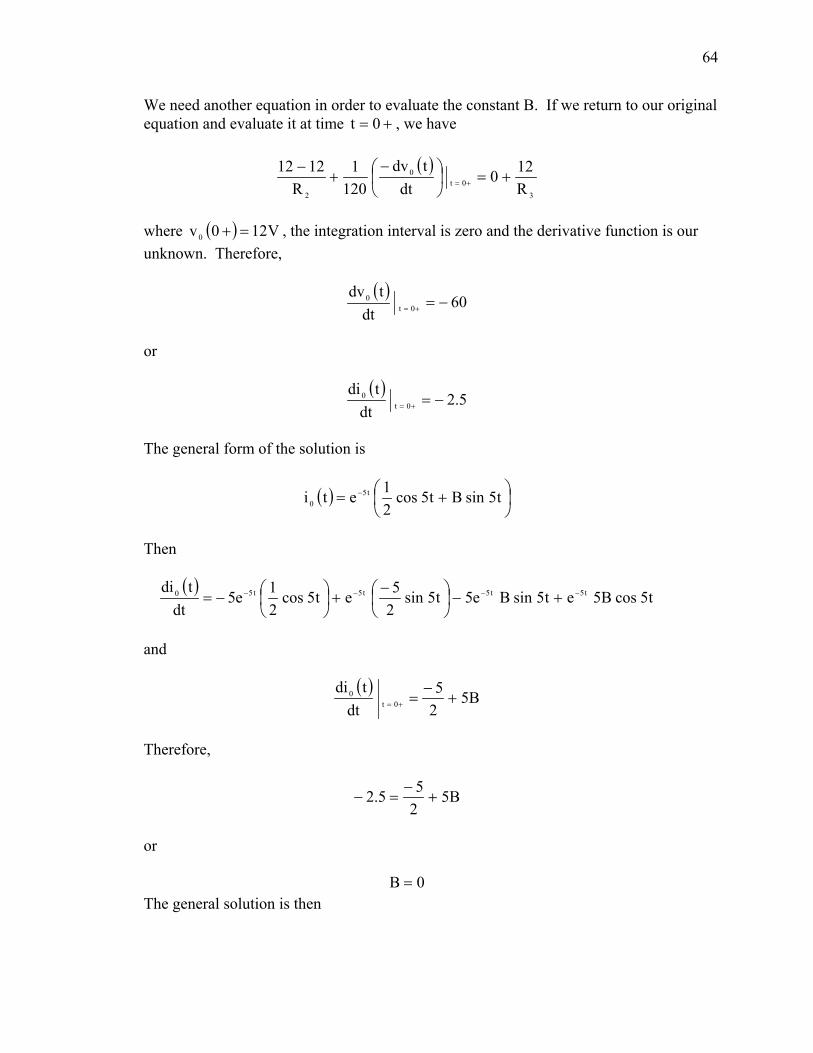
0.6
-0.2
0
0.2
0.4
0.60 0.2 0.4 0.8 1t (sec)
I 0 (t)
(A)
Fig. S7.6(b)
66
CHAPTER 8 PROBLEMS 8.1 Find the frequency domain impedance Z, shown in Fig. 8.1.
1Ω
j1ΩZ
1Ω
1Ω
-j1Ω
Fig. 8.1
8.2 If the impedance of the network in Fig. 8.2 is real at f = 60Hz, what is the value of the
inductor L?
2ΩL
Z
1Ω
10mF
Fig. 8.2
8.3 Use nodal analysis to find 0V in the network in Fig. 8.3.
2Ω1Ω
-j4Ω
- +
1Ωj2Ω
+
-
V012 °∠
0V
Fig. 8.3
8.4 Find 0V in the network in Fig. 8.4 using (a) loop analysis (b) superposition and (c)
Thevenin’s Theorem.
-+
4Ω
j2Ω
+
-
A02 °∠
0VV012 °∠
2Ω -j1Ω
Fig. 8.4
67
CHAPTER 8 SOLUTIONS 8.1. To begin our analysis, we note that the circuit can be labeled as shown in Fig. S8.1.
1Z
2Z 3ZZ
Fig. S8.1
In this case, Z1 consists of a 1Ω resistor, Z2 is the series combination of a 1Ω resistor and
a j1Ω inductor and Z2 consists of a –j1Ω capacitor in series with a 1Ω resistor. Therefore,
Z1 = 1Ω
Z2 = 1 + j1Ω Z3 = 1 – j1Ω
Starting at the opposite end of the network from the terminals at which Z is calculated we
note that Z2 and Z3 are in parallel and their combination is in series with Z1. Hence
( ) ( )
Ω=
+=
−++−+
+=
+=
2221
j1j1j1j11
ZZZZ 321
8.2 The general expression for the impedance of this network is
⎟⎟⎠
⎞⎜⎜⎝
⎛ω
+ω+=Cj
1Lj21Z
In order for Z to be purely resistive, the term ⎟⎟⎠
⎞⎜⎜⎝
⎛ω
+ωCj
1Lj must be real, i.e.
ZLC = RLC + j0
However, since ZLC can be written as
⎟⎠⎞
⎜⎝⎛
ω−ω=
C1LjZLC
68
it is clearly an imaginary term and RLC = 0. Therefore, in order for Z to be resistive
0C
1L =ω
−ω
or
( ) ( )H6.70310377
1C
1L
22
2
µ=
=
ω=
−
8.3 The presence of the voltage source indicates that nodal analysis is a viable approach to
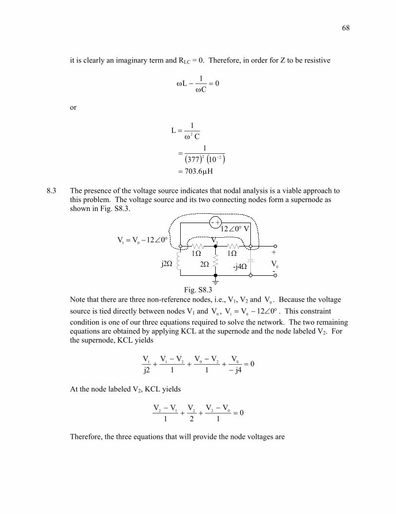
this problem. The voltage source and its two connecting nodes form a supernode as shown in Fig. S8.3.
V012 °∠
+
-0V
- +
-j4Ω
1Ω1Ω2Ωj2Ω
°∠−= 012VV 01 2V
Fig. S8.3
Note that there are three non-reference nodes, i.e., V1, V2 and 0V . Because the voltage source is tied directly between nodes V1 and 0V , °∠−= 012VV 01 . This constraint condition is one of our three equations required to solve the network. The two remaining equations are obtained by applying KCL at the supernode and the node labeled V2. For the supernode, KCL yields
04j
V1
VV1
VV2j
V 020211 =−
+−
+−
+
At the node labeled V2, KCL yields
01
VV2
V1
VV 02212 =−
++−
Therefore, the three equations that will provide the node voltages are
69
0VVV21VV
0V41jVVVVV
21j
12VV
02212
020211
01
=−++−
=+−+−+−
−=
Substituting the first equation in for the two remaining equations and combining terms
yields
12V25V2
6j12V241j2V
20
20
−=+−
−=−⎟⎠⎞
⎜⎝⎛ −
Solving for V2 in this last equation and substituting it into the one above it, we obtain
( ) 6j4.225.0j4.0V0 −=− and hence
V2.3657.13V0 °−∠= 8.4 (a) Since the network has two loops, or in this case two meshes, we will need two
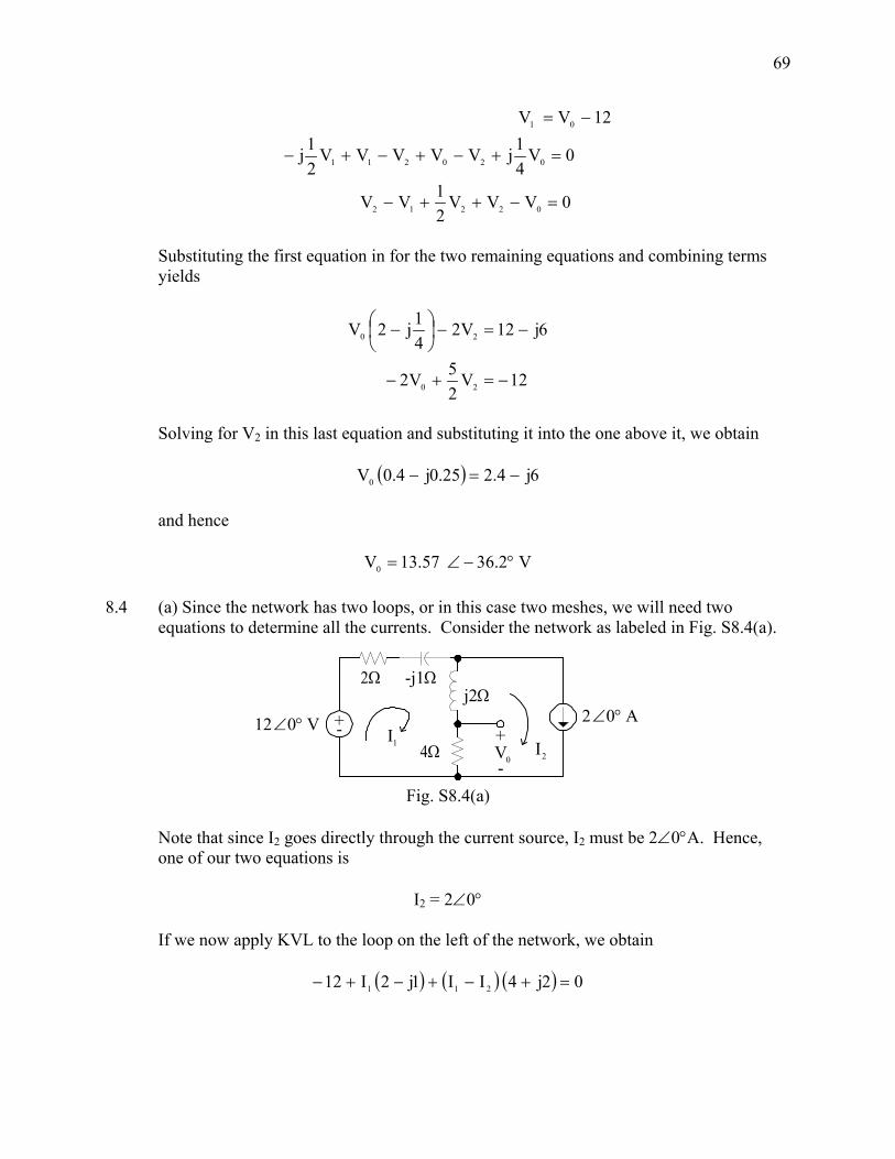
equations to determine all the currents. Consider the network as labeled in Fig. S8.4(a).
-+
4Ω
j2Ω
+
-
A02 °∠
0VV012 °∠
2Ω -j1Ω
1I2I
Fig. S8.4(a)
Note that since I2 goes directly through the current source, I2 must be 2∠0°A. Hence,
one of our two equations is
I2 = 2∠0° If we now apply KVL to the loop on the left of the network, we obtain
( ) ( ) ( ) 02j4II1j2I12 211 =+−+−+−
70
These two equations will yield the currents. Substituting the first equation into the second yields
( ) ( ) 02j422j41j2I12 1 =+−++−+−
and then
A85.135.31j64j20I1 °∠=
++
=
Finally,
( )
V57.442.5
21j64j204
II4V 210
°∠=
⎟⎟⎠
⎞⎜⎜⎝
⎛−
++
=
−=
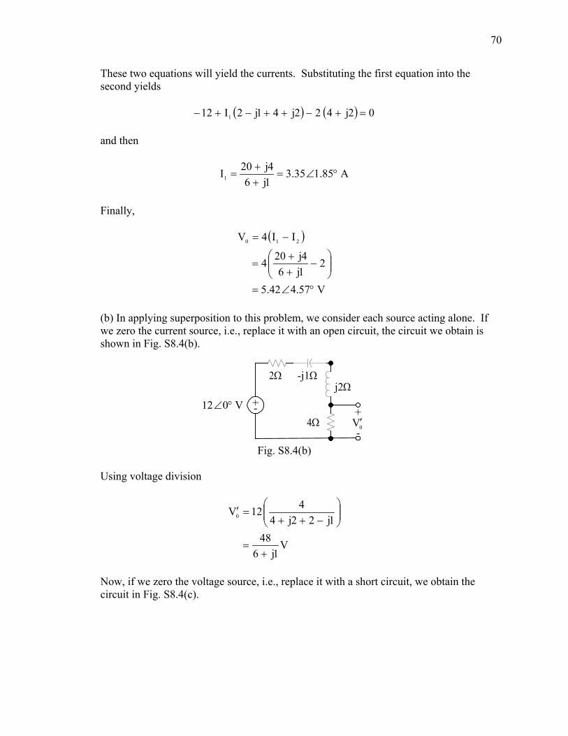
(b) In applying superposition to this problem, we consider each source acting alone. If
we zero the current source, i.e., replace it with an open circuit, the circuit we obtain is shown in Fig. S8.4(b).
-+
4Ω
j2Ω
+
-0V′V012 °∠
2Ω -j1Ω
Fig. S8.4(b)
Using voltage division
V1j6
481j22j4
412V0
+=
⎟⎟⎠
⎞⎜⎜⎝
⎛−++
=′
Now, if we zero the voltage source, i.e., replace it with a short circuit, we obtain the
circuit in Fig. S8.4(c).
71
4Ω
j2Ω
+
-0V ′′
A02 °∠
2Ω
-j1Ω
XI
Fig. S8.4(c)
Employing current division, the current IX is
A1j62j4
2j4j2j202IX
++−
=
⎟⎟⎠
⎞⎜⎜⎝
⎛++−
−°∠−=
Then,
1j68j16I4V X0 +
+−==′′
And finally,
V57.442.51j68j32
1j68j16
1j648
VVV 000
°∠=++
=
++−
++
=
′′+′=
(c) In applying Thevenin’s Theorem, we first break the network at the load and determine
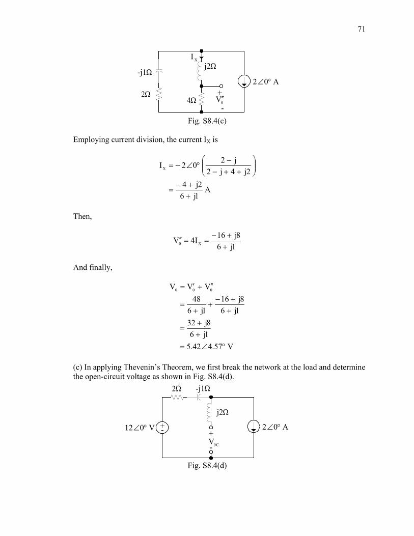
the open-circuit voltage as shown in Fig. S8.4(d).
j2Ω
+
- C0V
A02 °∠
2Ω -j1Ω
V012 °∠ +-
Fig. S8.4(d)
72
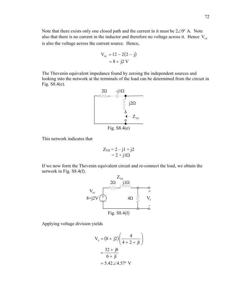
Note that there exists only one closed path and the current in it must be 2∠0° A. Note also that there is no current in the inductor and therefore no voltage across it. Hence OCV is also the voltage across the current source. Hence,
( )V2j8
j2212V C0
+=−−=
The Thevenin equivalent impedance found by zeroing the independent sources and
looking into the network at the terminals of the load can be determined from the circuit in Fig. S8.4(e).
j2Ω
THZ
2Ω -j1Ω
Fig. S8.4(e)
This network indicates that
ZTH = 2 – j1 + j2 = 2 + j1Ω If we now form the Thevenin equivalent circuit and re-connect the load, we obtain the
network in Fig. S8.4(f).
4Ω
THZ2Ω j1Ω
+-
-
+
0VC0V
8+j2V
Fig. S8.4(f)
Applying voltage division yields
( )
V57.442.51j68j32
1j2442j8V0
°∠=++
=
⎟⎟⎠
⎞⎜⎜⎝
⎛++
+=
73
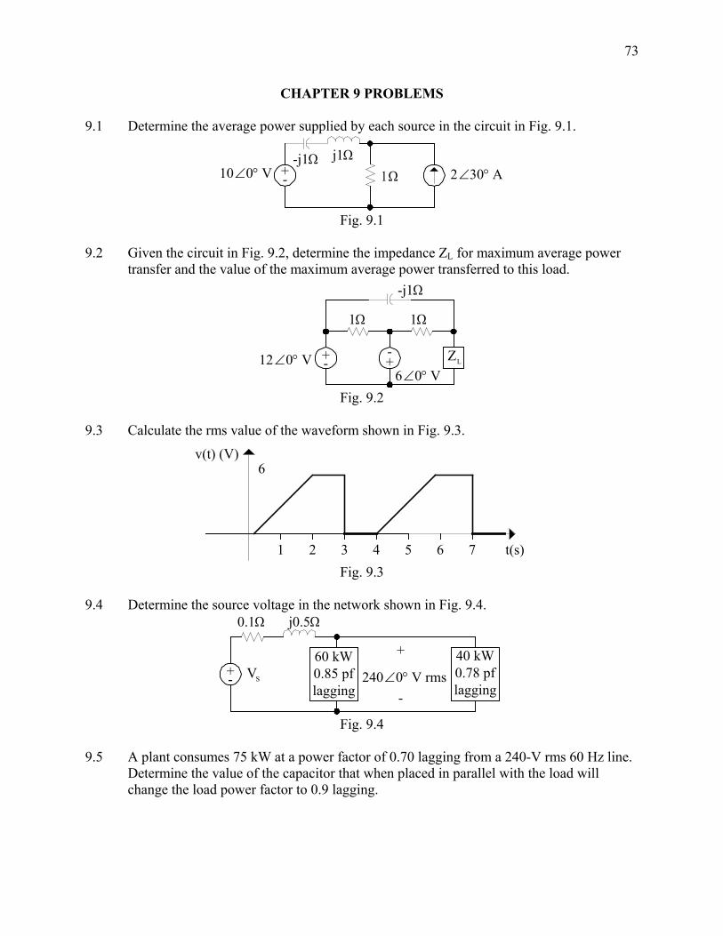
CHAPTER 9 PROBLEMS 9.1 Determine the average power supplied by each source in the circuit in Fig. 9.1.
1Ω+-
j1Ω-j1ΩV010 °∠ A302 °∠
Fig. 9.1
9.2 Given the circuit in Fig. 9.2, determine the impedance ZL for maximum average power
transfer and the value of the maximum average power transferred to this load.
V06 °∠
1Ω 1Ω
-j1Ω
V012 °∠ LZ+ +--
Fig. 9.2
9.3 Calculate the rms value of the waveform shown in Fig. 9.3.
1 t(s)765432
6v(t) (V)
Fig. 9.3
9.4 Determine the source voltage in the network shown in Fig. 9.4.
SV rmsV0240 °∠40 kW0.78 pflagging
60 kW0.85 pflagging
+-
+
-
0.1Ω j0.5Ω
Fig. 9.4
9.5 A plant consumes 75 kW at a power factor of 0.70 lagging from a 240-V rms 60 Hz line.
Determine the value of the capacitor that when placed in parallel with the load will change the load power factor to 0.9 lagging.
74
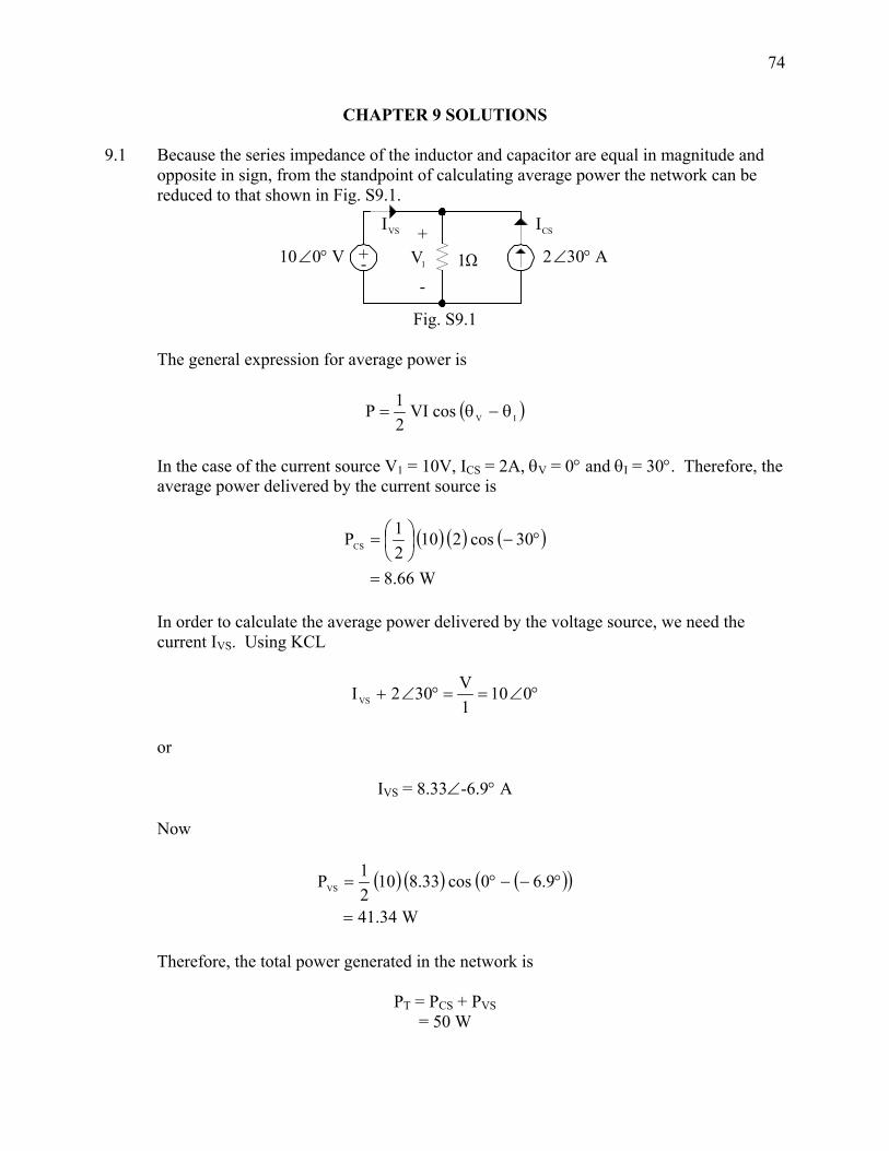
CHAPTER 9 SOLUTIONS 9.1 Because the series impedance of the inductor and capacitor are equal in magnitude and
opposite in sign, from the standpoint of calculating average power the network can be reduced to that shown in Fig. S9.1.
CSI
A302 °∠+
V010 °∠
-
+- 1Ω
VSI
1V
Fig. S9.1
The general expression for average power is
( )IVcosVI21P θ−θ=
In the case of the current source V1 = 10V, ICS = 2A, θV = 0° and θI = 30°. Therefore, the
average power delivered by the current source is
( ) ( ) ( )
W66.8
30cos21021PCS
=
°−⎟⎠⎞
⎜⎝⎛=
In order to calculate the average power delivered by the voltage source, we need the
current IVS. Using KCL
°∠==°∠+ 0101V302IVS
or
IVS = 8.33∠-6.9° A Now
( ) ( ) ( )( )
W34.41
9.60cos33.81021PVS
=
°−−°=
Therefore, the total power generated in the network is
PT = PCS + PVS = 50 W

75
Let us now calculate the average power absorbed by the resistor. We know that the
average power absorbed by the resistor must be
W501
1021
RV
21P
2
2m
R
=
⎟⎠
⎞⎜⎝
⎛=
=
In addition, the average power absorbed by the resistor can also be determined by
RI21P 2
mR =
However, we do not know the current in the resistor. Using KCL. IR = IVS + ICS
= 8.66∠-6.9° + 2∠30° = 10∠0° A Now
( ) ( )
W50
11021P 2
R
=
=
Thus, we find that the total average power generated is equal to the average power
absorbed. 9.2 We will first determine the Thevenin equivalent circuit for the network without the load
attached. The open-circuit voltage, V0C, can be determined from the network in Fig. S9.2(a).
C0VV012 °∠ +-
1Ω
RV
1Ω
-+
-j1Ω
++
-
-I
V06 °∠
Fig. S9.2(a) This open-circuit voltage can be calculated in a number of ways. For example, we can
compute the current I as
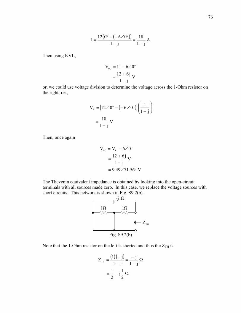
76
( )( ) A
j118
j106012I
−=
−°∠−−°
=
Then using KVL,
Vj1
j61206I1V C0
−+
=
°∠−=
or, we could use voltage division to determine the voltage across the 1-Ohm resistor on the right, i.e.,
( )[ ]
Vj1
18j1
106012VR
−=
⎟⎟⎠
⎞⎜⎜⎝
⎛−
°∠−−°∠=
Then, once again
V56.7149.9
Vj1
j61206VV RC0
°∠=−+
=
°∠−=
The Thevenin equivalent impedance is obtained by looking into the open-circuit
terminals with all sources made zero. In this case, we replace the voltage sources with short circuits. This network is shown in Fig. S9.2(b).
THZ
1Ω 1Ω
-j1Ω
Fig. S9.2(b)
Note that the 1-Ohm resistor on the left is shorted and thus the ZTH is
( ) ( )
Ω−=
Ω−−
=−−
=
21j
21
j1j
j1j1ZTH
77
Hence, for maximum average power transfer
*THL ZZ =
or
Ω+=21j
21ZL
Therefore, the network is reduced to that shown in Fig. S9.2(c).
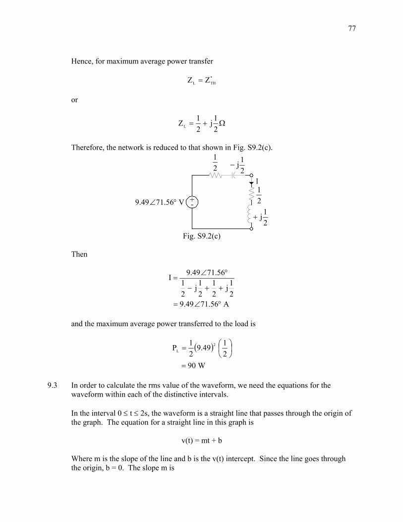
Ι
+-V56.7149.9 °∠ 21
21
21j+
21j−
Fig. S9.2(c)
Then
A56.7149.921j
21
21j
21
56.7149.9I
°∠=
++−
°∠=
and the maximum average power transferred to the load is
( )
W902149.9
21P 2
L
=
⎟⎠⎞
⎜⎝⎛=
9.3 In order to calculate the rms value of the waveform, we need the equations for the
waveform within each of the distinctive intervals. In the interval 0 ≤ t ≤ 2s, the waveform is a straight line that passes through the origin of
the graph. The equation for a straight line in this graph is
v(t) = mt + b Where m is the slope of the line and b is the v(t) intercept. Since the line goes through
the origin, b = 0. The slope m is
78
3s2V6m ==
Therefore, in the interval 0 ≤ t ≤ 2s,
v(t) = 3t The waveform has constant values in the intervals 2 ≤ t ≤ 3s and 3 ≤ t ≤ 4s, i.e.,
v(t) = 6 2 ≤ t ≤ 3s v(t) = 0 3 ≤ t ≤ 4s
Since the waveform repeats after 4s, the period of the waveform is
T = 4s Now that the data for the waveform is known,
( ) 214
0
2rms dttv
T1V ⎥⎦
⎤⎢⎣⎡
∫=
Therefore, in this case
( ) ( ) ( )
[ ]
( )
( )rmsV87.3
15
362441
t36t341
dt0dt6dtt341V
21
21
21
32
20
3
214
3
23
2
22
0
2rms
==
⎥⎦⎤
⎢⎣⎡ +=
⎥⎦⎤
⎢⎣⎡ +=
⎥⎦⎤
⎢⎣⎡
⎥⎦⎤
⎢⎣⎡ ∫+∫+∫=
9.4 We begin our analysis by labeling the various currents and voltages in the circuit as
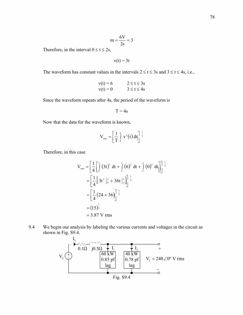
shown in Fig. S9.4.
SV 40 kW0.78 pf
lag
60 kW0.85 pf
lag
+-
+
-
0.1Ω j0.5Ω
SI
1I 2I
rmsV0240VL °∠=
Fig. S9.4
79
Our approach to determining VS is straight forward: We will compute the currents I1 and I2; add them using KCL to find IS; determine the voltage across the line impedance and finally use KVL to add the line voltage and load voltage to determine the source voltage.
The magnitude of the current I1 is
( )
( ) ( ).rmsA12.294
85.0240000,60pfV
PI1L
11
=
=
=
And the phase angle is
( )°−=
−=θ −
79.31
85.0cos 1I1
The negative sign is a result of the fact that the power factor is lagging. Thus
I1 = 294.12∠-31.79° A rms. The magnitude of the current I2 is
( )
( ) ( ).rmsA68.213
78.0240000,40pfV
PI2L
22
=
=
=
And the phase angle is
( )°−=
−=θ −
74.38
78.0cos 1I2
Thus
I2 = 213.68∠-38.74° A rms. Using KCL
80
.rmsA25.341.50474.3868.21379.3112.294
III 21S
°−∠=°−∠+°−∠=
+=
Then
( )( ) ( )
.rmsV02.2317.460024044.4404.257
02407.7851.025.341.50402405.0j1.0IV S2
°∠=°∠+°∠=
°∠+°∠°−∠=°∠++=
9.5 Since the original power factor is 0.7 lagging the power factor angle is
θOLD = cos-1 (0.7) = 45.57° Then
QOLD = POLD tan θOLD = 75,000 tan 45.57° = 76.52 kvar Hence
SOLD = 75,000 + j76,515 = 107.14∠45.57° kVA The new power factor angle we wish to achieve is
θNEW = cos-1 (new power factor) = cos-1 (0.9) = 25.84° Then
QNEW = POLD tan θNEW = 75,000 tan 25.84° = 36,324 kvar Now the difference between QNEW and QOLD is achieved by the capacitor, i.e.,
QCAP = QNEW - QOLD = 36,324 – 76,515 = -40,191 kvar
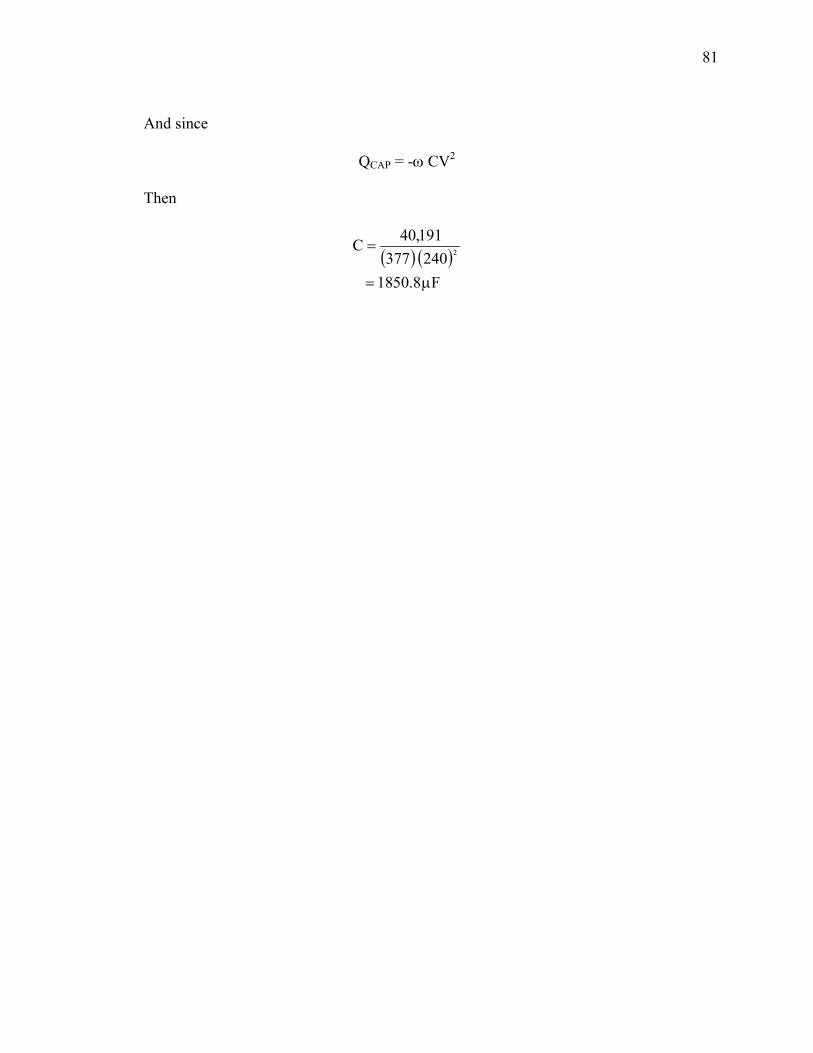
81
And since
QCAP = -ω CV2 Then
( ) ( )F8.1850
240377191,40C 2
µ=
=
82
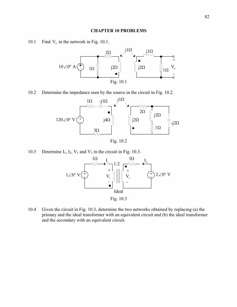
CHAPTER 10 PROBLEMS 10.1 Find 0V in the network in Fig. 10.1.
j1Ω
1Ωj2Ω
j1Ω
-
+
0VA010 °∠
2Ω
j2Ω1Ω
Fig. 10.1
10.2 Determine the impedance seen by the source in the circuit in Fig. 10.2.
j1Ω
1Ω
j2Ωj2Ω
V0120 °∠
1Ω
j4Ω
3Ω
-j1Ω
+-
2Ω
-j2Ω
Fig. 10.2
10.3 Determine I1, I2, V1 and V2 in the circuit in Fig. 10.3.
1:2
Ideal
V01 °∠
1Ω
+-
3Ω
+
-1V
1I 2I
+
-2V V02 °∠+-
Fig. 10.3
10.4 Given the circuit in Fig. 10.3, determine the two networks obtained by replacing (a) the
primary and the ideal transformer with an equivalent circuit and (b) the ideal transformer and the secondary with an equivalent circuit.
83
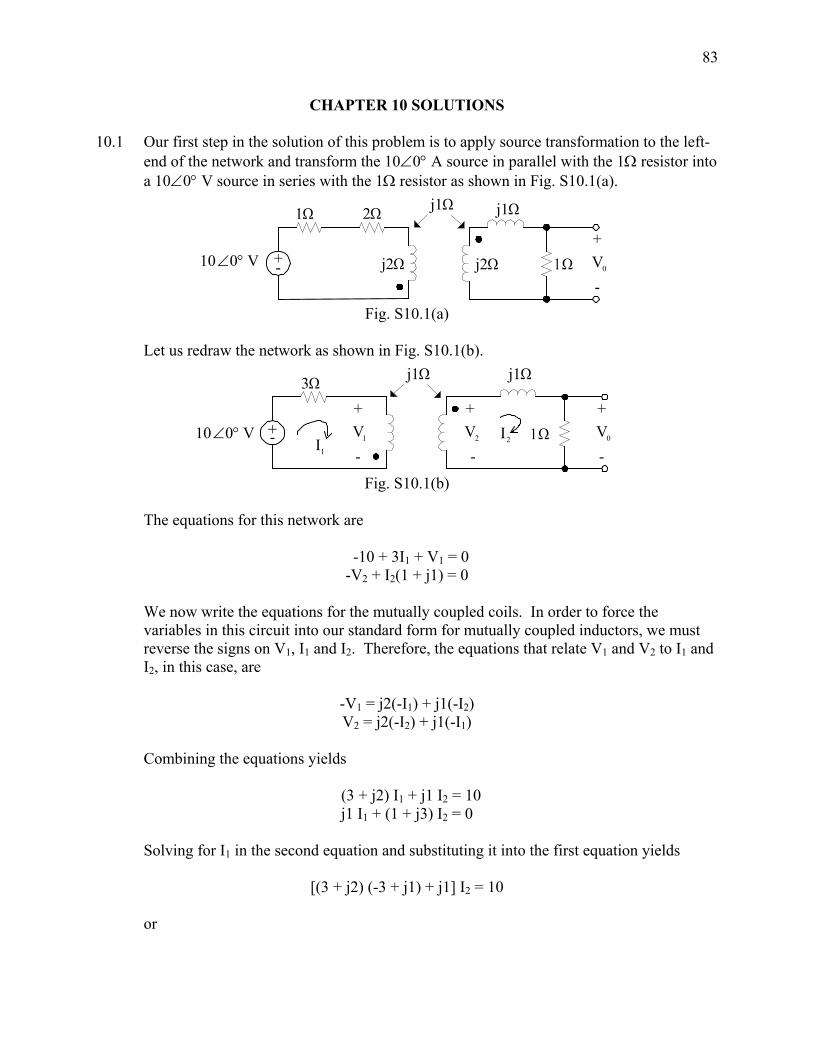
CHAPTER 10 SOLUTIONS 10.1 Our first step in the solution of this problem is to apply source transformation to the left-
end of the network and transform the 10∠0° A source in parallel with the 1Ω resistor into a 10∠0° V source in series with the 1Ω resistor as shown in Fig. S10.1(a).
j1Ω
1Ωj2Ω
j1Ω
-
+
0VV010 °∠
2Ω
j2Ω
1Ω
-+
Fig. S10.1(a)
Let us redraw the network as shown in Fig. S10.1(b).
j1Ω
1Ω
j1Ω
-
+
0VV010 °∠
3Ω
-+
-
+
1V1I -
+
2V2I
Fig. S10.1(b)
The equations for this network are -10 + 3I1 + V1 = 0
-V2 + I2(1 + j1) = 0 We now write the equations for the mutually coupled coils. In order to force the
variables in this circuit into our standard form for mutually coupled inductors, we must reverse the signs on V1, I1 and I2. Therefore, the equations that relate V1 and V2 to I1 and I2, in this case, are
-V1 = j2(-I1) + j1(-I2) V2 = j2(-I2) + j1(-I1)
Combining the equations yields (3 + j2) I1 + j1 I2 = 10
j1 I1 + (1 + j3) I2 = 0 Solving for I1 in the second equation and substituting it into the first equation yields
[(3 + j2) (-3 + j1) + j1] I2 = 10 or
84
A3.10894.02j11
10I2
°∠−=−−
=
And finally
V3.10894.0I1V 20
°∠−==
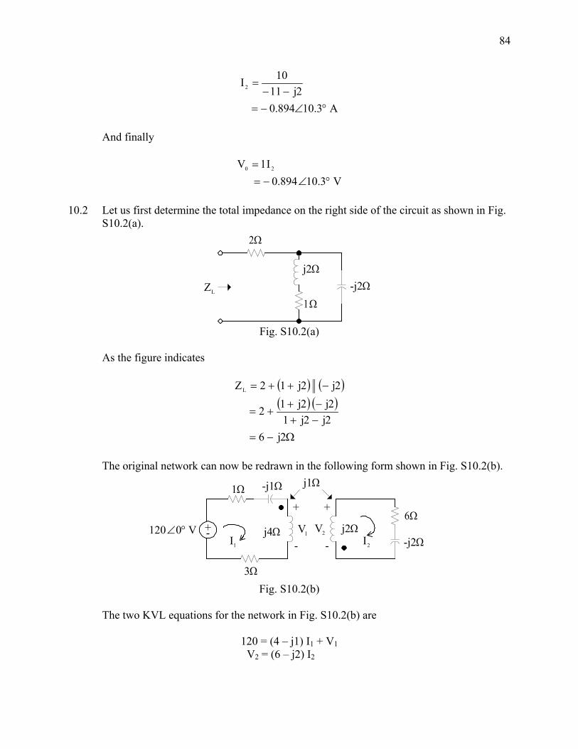
10.2 Let us first determine the total impedance on the right side of the circuit as shown in Fig.
S10.2(a).
j2Ω
LZ
2Ω
-j2Ω
1Ω
Fig. S10.2(a) As the figure indicates
( ) ( )( ) ( )
Ω−=−+−+
+=
−++=
2j62j2j12j2j12
2j2j12ZL
The original network can now be redrawn in the following form shown in Fig. S10.2(b).
j1Ω
6Ω
-j2ΩV0120 °∠
1Ω
-+-
+
1V1I -
+
2V2I
-j1Ω
j4Ω
3Ω
j2Ω
Fig. S10.2(b)
The two KVL equations for the network in Fig. S10.2(b) are
120 = (4 – j1) I1 + V1 V2 = (6 – j2) I2
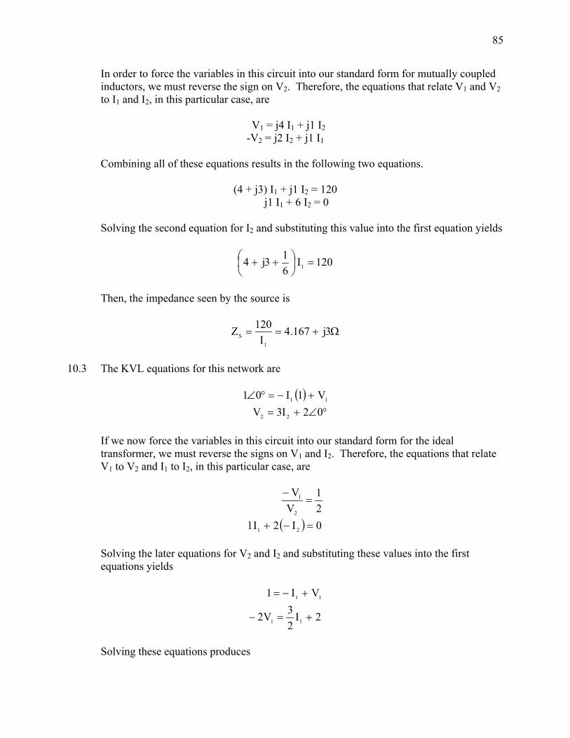
85
In order to force the variables in this circuit into our standard form for mutually coupled inductors, we must reverse the sign on V2. Therefore, the equations that relate V1 and V2 to I1 and I2, in this particular case, are
V1 = j4 I1 + j1 I2
-V2 = j2 I2 + j1 I1 Combining all of these equations results in the following two equations.
(4 + j3) I1 + j1 I2 = 120 j1 I1 + 6 I2 = 0 Solving the second equation for I2 and substituting this value into the first equation yields
120I613j4 1 =⎟
⎠⎞
⎜⎝⎛ ++
Then, the impedance seen by the source is
Ω+== 3j167.4I
120Z1
S
10.3 The KVL equations for this network are
( )°∠+=
+−=°∠02I3VV1I01
22
11
If we now force the variables in this circuit into our standard form for the ideal
transformer, we must reverse the signs on V1 and I2. Therefore, the equations that relate V1 to V2 and I1 to I2, in this particular case, are
( ) 0I2I121
VV
21
2
1
=−+
=−
Solving the later equations for V2 and I2 and substituting these values into the first
equations yields
2I23V2
VI1
11
11
+=−
+−=
Solving these equations produces
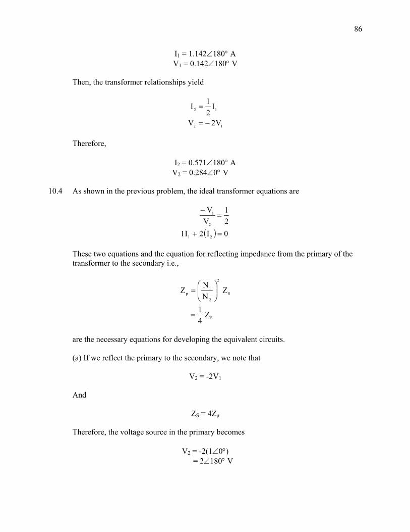
86
I1 = 1.142∠180° A V1 = 0.142∠180° V
Then, the transformer relationships yield
12
12
V2V
I21I
−=
=
Therefore,
I2 = 0.571∠180° A V2 = 0.284∠0° V 10.4 As shown in the previous problem, the ideal transformer equations are
( ) 0I2I121
VV
21
2
1
=+
=−
These two equations and the equation for reflecting impedance from the primary of the
transformer to the secondary i.e.,
S
S
2
2
1p
Z41
ZNNZ
=
⎟⎟⎠
⎞⎜⎜⎝
⎛=
are the necessary equations for developing the equivalent circuits. (a) If we reflect the primary to the secondary, we note that
V2 = -2V1 And
ZS = 4Zp Therefore, the voltage source in the primary becomes
V2 = -2(1∠0°) = 2∠180° V
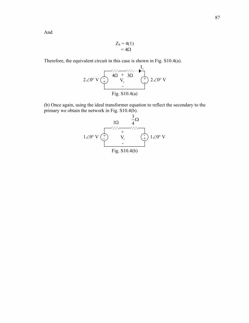
87
And
ZS = 4(1) = 4Ω Therefore, the equivalent circuit in this case is shown in Fig. S10.4(a).
2I
V02 °∠V02 °∠2V
4Ω 3Ω+
-+- +
-
Fig. S10.4(a) (b) Once again, using the ideal transformer equation to reflect the secondary to the
primary we obtain the network in Fig. S10.4(b).
Ω43
V01 °∠V01 °∠1V
1Ω
+
-+- +
-
Fig. S10.4(b)
88
CHAPTER 11 PROBLEMS 11.1 In a three-phase balanced wye-wye system, the source is an abc-sequence set of voltages
with Van = 120∠40° V rms. The per phase impedance of the load is 10 + j8Ω. If the line impedance per phase is 0.6 + j0.4Ω, find the line currents and load voltages.
11.2 An abc-sequence set of voltages feeds a balanced three-phase wye-wye system. If Van =
440∠40° V rms, VAN = 410∠39° V rms and the line impedance is 1.5 + j1.0Ω, find the load impedance.
11.3 In a balanced three-phase wye-delta system, the source has an abc-phase sequence and
Van = 120∠30° V rms. The line and load impedance are 0.6 + j0.4Ω and 24 + j12Ω, respectively. Find the delta currents in the load.
11.4 A balanced three-phase source serves two loads: Load 1: 32 kVA at 0.85 pf lagging. Load 2: 20 kVA at 0.6 pf lagging. The line voltage at the load is 208 V rms at 60Hz. Determine the line current and the
combined power factor at the load. 11.5 In a three-phase balanced system an abc-sequence wye-connected source with Van =
220∠0° V rms supplies power to a wye-connected load that consumes 36 kW of power in each phase at a pf of 0.75 lagging. Three capacitors, each with an impedance of –j2.0Ω, are connected in parallel with the original load in a wye configuration. Determine the power factor of the combined load as seen by the source.
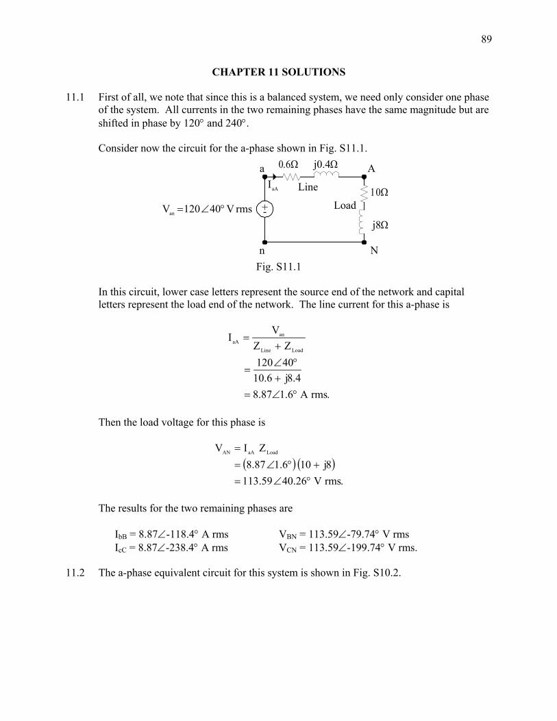
89
CHAPTER 11 SOLUTIONS 11.1 First of all, we note that since this is a balanced system, we need only consider one phase
of the system. All currents in the two remaining phases have the same magnitude but are shifted in phase by 120° and 240°.
Consider now the circuit for the a-phase shown in Fig. S11.1.
10Ω
0.6Ω j0.4Ω
+-
n
a
rmsV40120Van °∠=j8Ω
A
N
Load
LineaAI
Fig. S11.1
In this circuit, lower case letters represent the source end of the network and capital
letters represent the load end of the network. The line current for this a-phase is
.rmsA6.187.84.8j6.10
40120ZZ
VI
LoadLine
anaA
°∠=+
°∠=
+=
Then the load voltage for this phase is
( ) ( ).rmsV26.4059.113
8j106.187.8ZIV LoadaAAN
°∠=+°∠=
=
The results for the two remaining phases are IbB = 8.87∠-118.4° A rms VBN = 113.59∠-79.74° V rms IcC = 8.87∠-238.4° A rms VCN = 113.59∠-199.74° V rms. 11.2 The a-phase equivalent circuit for this system is shown in Fig. S10.2.
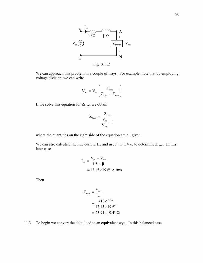
90
+1.5Ω j1Ω
+-
n
a
anV
-
A
N
ANVLOADZ
aAI
Fig. S11.2
We can approach this problem in a couple of ways. For example, note that by employing
voltage division, we can write
⎥⎦
⎤⎢⎣
⎡+
=LineLoad
LoadanAN ZZ
ZVV
If we solve this equation for ZLoad, we obtain
1VVZ
Z
AN
an
LineLoad
−=
where the quantities on the right side of the equation are all given. We can also calculate the line current IaA and use it with VAN to determine ZLoad. In this
later case
rmsA6.1915.171j5.1
VVI ANan
aA
°∠=+
−=
Then
Ω°∠=°∠
°∠=
=
4.1991.236.1915.17
39410IV
ZaA
ANLoad
11.3 To begin we convert the delta load to an equivalent wye. In this balanced case
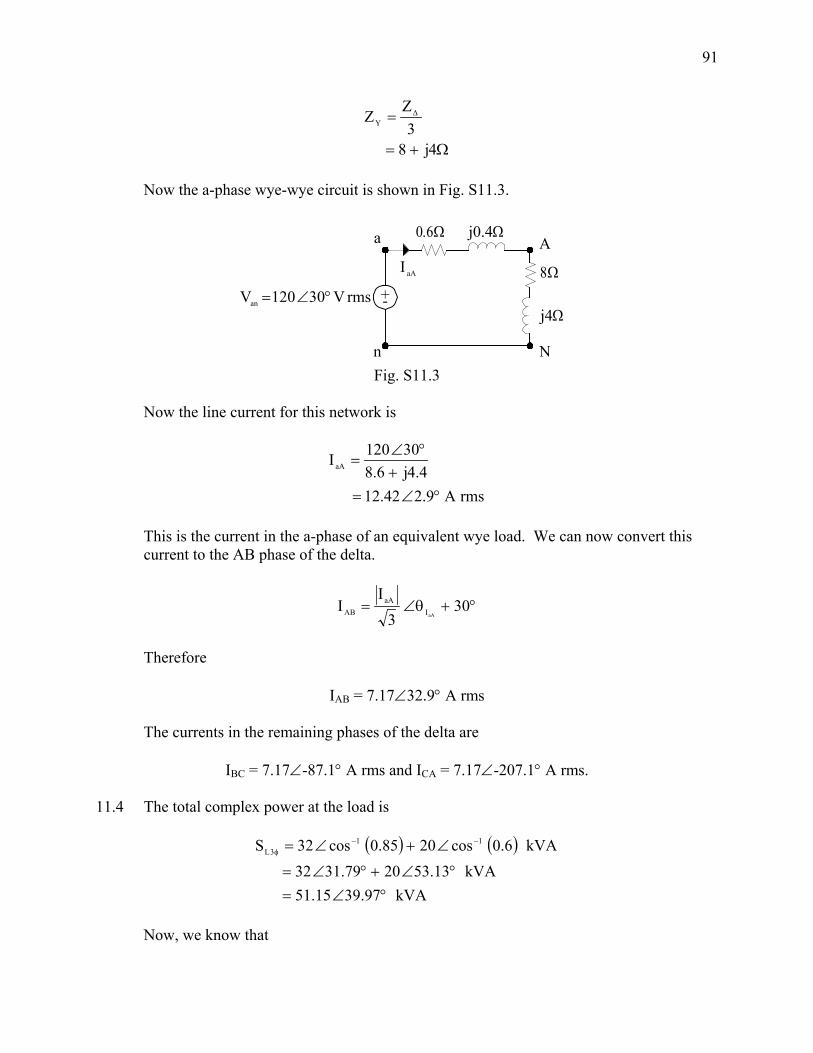
91
Ω+=
= ∆
4j83
ZZY
Now the a-phase wye-wye circuit is shown in Fig. S11.3.
8Ω
0.6Ω j0.4Ω
+-
n
a
rmsV30120Van °∠=j4Ω
A
N
aAI
Fig. S11.3
Now the line current for this network is
rmsA9.242.124.4j6.8
30120IaA
°∠=+
°∠=
This is the current in the a-phase of an equivalent wye load. We can now convert this
current to the AB phase of the delta.
°+θ∠= 303
II
aAIaA
AB
Therefore
IAB = 7.17∠32.9° A rms The currents in the remaining phases of the delta are
IBC = 7.17∠-87.1° A rms and ICA = 7.17∠-207.1° A rms. 11.4 The total complex power at the load is
( ) ( )
kVA97.3915.51kVA13.532079.3132
kVA6.0cos2085.0cos32S 113L
°∠=°∠+°∠=
∠+∠= −−φ
Now, we know that
92
LL3L IV3S =φ And hence
( )rmsA98.141
2083k15.51IL
=
=
And the power factor at the load is
pfLoad = cos(39.97°) = 0.766 lagging 11.5 The original situation, prior to adding the capacitors is
POLD = 36 kW
QOLD = POLD tAN θOLD = 36,000 tan 41.41° = 31,749 var where 41.41° = θOLD = cos-1 (0.75). Therefore,
SOLD = 36 + j31.749 kVA is the complex power for each phase. If we now add the capacitor, the real power is unaffected by this and thus
PNEW = POLD = 36 kW However,
QNEW = QOLD + QC Where QC is the reactive power supplied by the capacitor.
C
2
2C
ZrmsV
rmsCVjQ−
=
ω−=
or
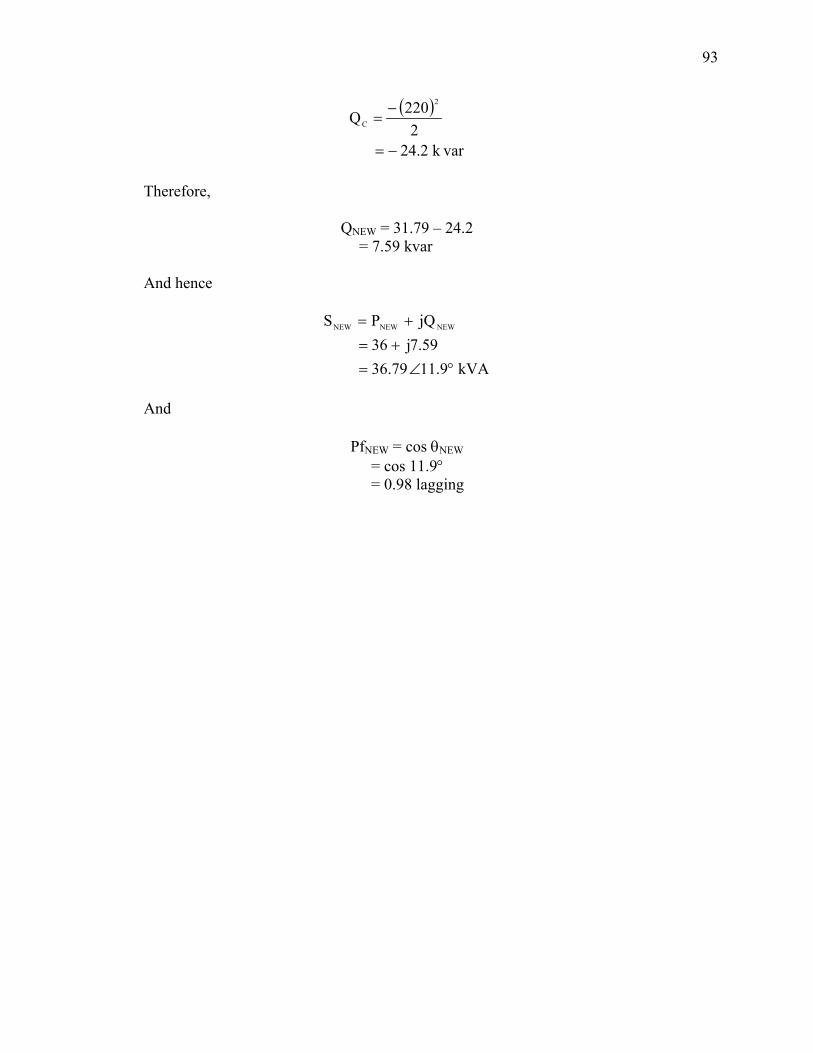
93
( )
vark2.242
220Q2
C
−=
−=
Therefore,
QNEW = 31.79 – 24.2 = 7.59 kvar And hence
kVA9.1179.3659.7j36jQPS NEWNEWNEW
°∠=+=
+=
And
PfNEW = cos θNEW = cos 11.9° = 0.98 lagging
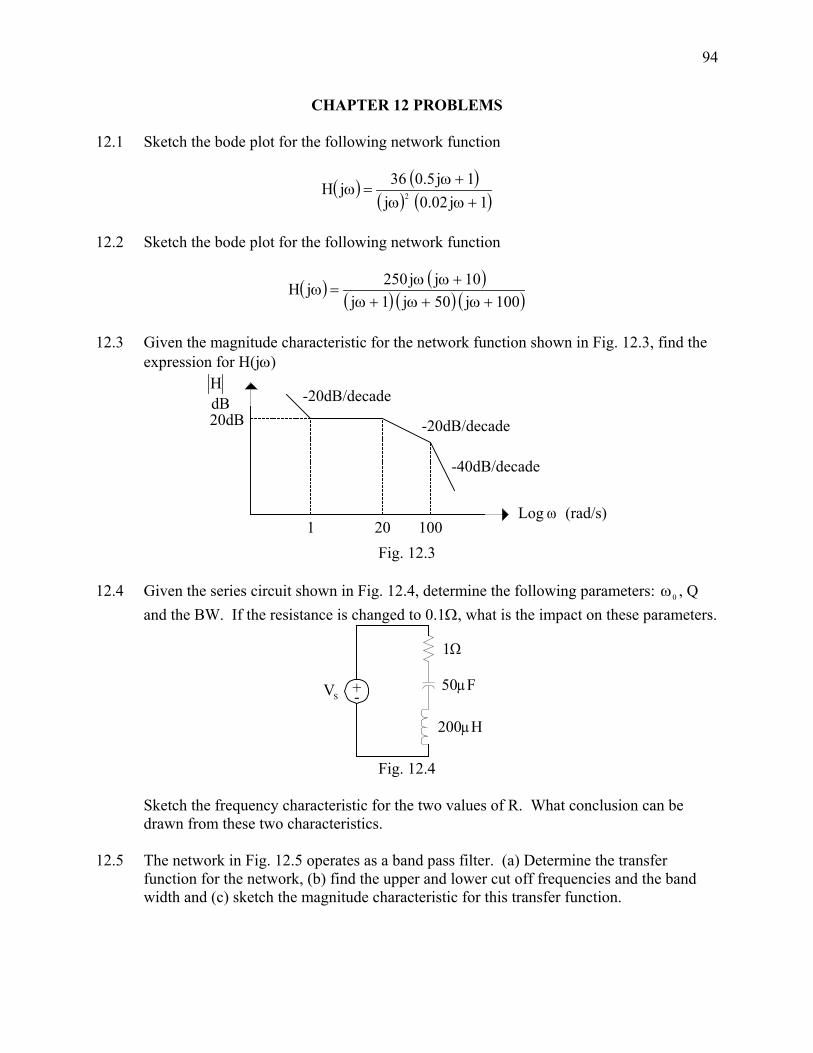
94
CHAPTER 12 PROBLEMS 12.1 Sketch the bode plot for the following network function
( ) ( )( ) ( )1j02.0j
1j5.036jH 2 +ωω+ω
=ω
12.2 Sketch the bode plot for the following network function
( ) ( )( ) ( ) ( )100j50j1j
10jj250jH+ω+ω+ω
+ωω=ω
12.3 Given the magnitude characteristic for the network function shown in Fig. 12.3, find the
expression for H(jω) HdB20dB
-20dB/decade
Log ω1 20 100
-20dB/decade
-40dB/decade
(rad/s)
Fig. 12.3 12.4 Given the series circuit shown in Fig. 12.4, determine the following parameters: 0ω , Q
and the BW. If the resistance is changed to 0.1Ω, what is the impact on these parameters.
1Ω
+-50µF
200µH
SV
Fig. 12.4
Sketch the frequency characteristic for the two values of R. What conclusion can be
drawn from these two characteristics. 12.5 The network in Fig. 12.5 operates as a band pass filter. (a) Determine the transfer
function for the network, (b) find the upper and lower cut off frequencies and the band width and (c) sketch the magnitude characteristic for this transfer function.
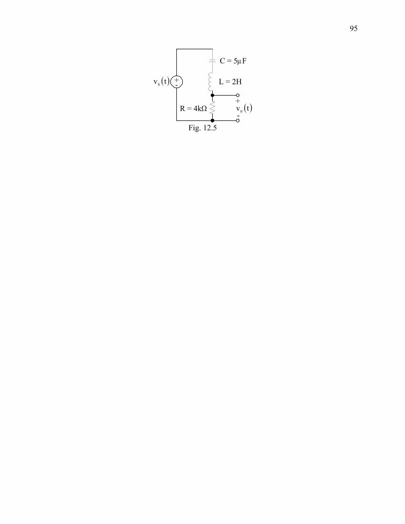
95
C = 5µF
+- L = 2H
R = 4kΩ
( )tvS
-
+( )tv0
Fig. 12.5
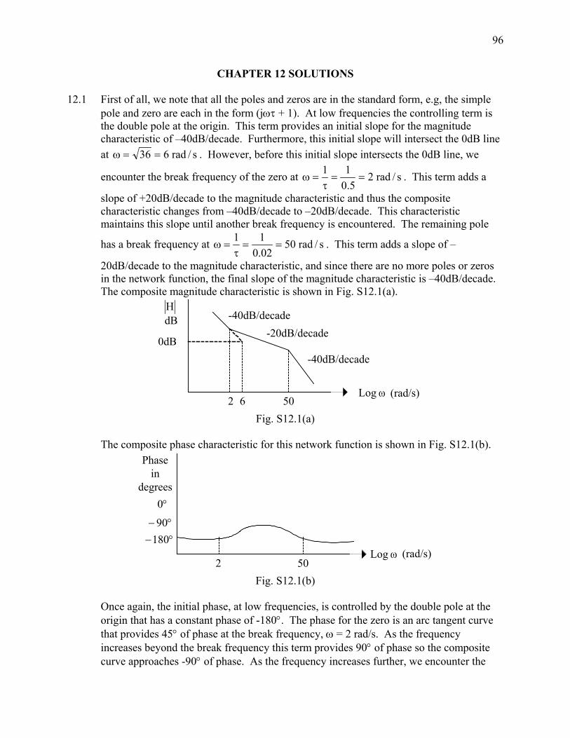
96
CHAPTER 12 SOLUTIONS 12.1 First of all, we note that all the poles and zeros are in the standard form, e.g, the simple
pole and zero are each in the form (jωτ + 1). At low frequencies the controlling term is the double pole at the origin. This term provides an initial slope for the magnitude characteristic of –40dB/decade. Furthermore, this initial slope will intersect the 0dB line at s/rad636 ==ω . However, before this initial slope intersects the 0dB line, we
encounter the break frequency of the zero at s/rad25.0
11==
τ=ω . This term adds a
slope of +20dB/decade to the magnitude characteristic and thus the composite characteristic changes from –40dB/decade to –20dB/decade. This characteristic maintains this slope until another break frequency is encountered. The remaining pole
has a break frequency at s/rad5002.011
==τ
=ω . This term adds a slope of –
20dB/decade to the magnitude characteristic, and since there are no more poles or zeros in the network function, the final slope of the magnitude characteristic is –40dB/decade. The composite magnitude characteristic is shown in Fig. S12.1(a).
HdB
0dB
-40dB/decade
Log ω2 6 50
-20dB/decade
-40dB/decade
(rad/s)
Fig. S12.1(a) The composite phase characteristic for this network function is shown in Fig. S12.1(b).
Phasein
degrees°0
°−180°− 90
2 50Log ω (rad/s)
Fig. S12.1(b)
Once again, the initial phase, at low frequencies, is controlled by the double pole at the
origin that has a constant phase of -180°. The phase for the zero is an arc tangent curve that provides 45° of phase at the break frequency, ω = 2 rad/s. As the frequency increases beyond the break frequency this term provides 90° of phase so the composite curve approaches -90° of phase. As the frequency increases further, we encounter the
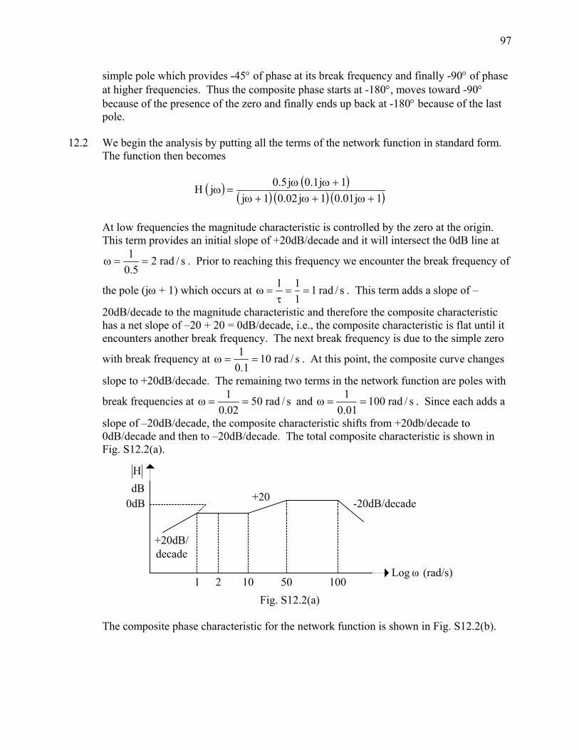
97
simple pole which provides -45° of phase at its break frequency and finally -90° of phase at higher frequencies. Thus the composite phase starts at -180°, moves toward -90° because of the presence of the zero and finally ends up back at -180° because of the last pole.
12.2 We begin the analysis by putting all the terms of the network function in standard form.
The function then becomes
( ) ( )( ) ( ) ( )1j01.01j02.01j
1j1.0j5.0jH+ω+ω+ω
+ωω=ω
At low frequencies the magnitude characteristic is controlled by the zero at the origin.
This term provides an initial slope of +20dB/decade and it will intersect the 0dB line at
s/rad25.0
1==ω . Prior to reaching this frequency we encounter the break frequency of
the pole (jω + 1) which occurs at s/rad1111
==τ
=ω . This term adds a slope of –
20dB/decade to the magnitude characteristic and therefore the composite characteristic has a net slope of –20 + 20 = 0dB/decade, i.e., the composite characteristic is flat until it encounters another break frequency. The next break frequency is due to the simple zero
with break frequency at s/rad101.0
1==ω . At this point, the composite curve changes
slope to +20dB/decade. The remaining two terms in the network function are poles with
break frequencies at s/rad5002.01
==ω and s/rad10001.01
==ω . Since each adds a
slope of –20dB/decade, the composite characteristic shifts from +20db/decade to 0dB/decade and then to –20dB/decade. The total composite characteristic is shown in Fig. S12.2(a).
HdB
0dB
+20dB/decade
Log ω1 10 100
-20dB/decade+20
2 50(rad/s)
Fig. S12.2(a)
The composite phase characteristic for the network function is shown in Fig. S12.2(b).
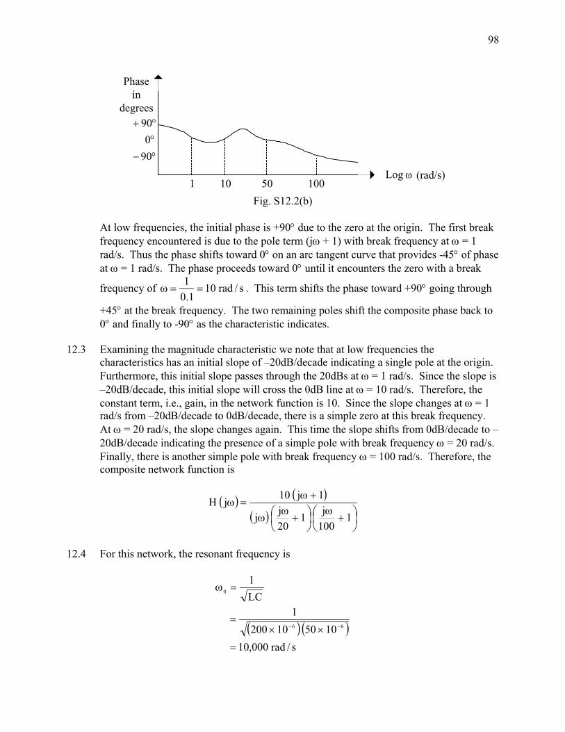
98
Phasein
degrees
°0°− 90
1 50Log ω
°+ 90
10 100(rad/s)
Fig. S12.2(b)
At low frequencies, the initial phase is +90° due to the zero at the origin. The first break
frequency encountered is due to the pole term (jω + 1) with break frequency at ω = 1 rad/s. Thus the phase shifts toward 0° on an arc tangent curve that provides -45° of phase at ω = 1 rad/s. The phase proceeds toward 0° until it encounters the zero with a break
frequency of s/rad101.0
1==ω . This term shifts the phase toward +90° going through
+45° at the break frequency. The two remaining poles shift the composite phase back to 0° and finally to -90° as the characteristic indicates.
12.3 Examining the magnitude characteristic we note that at low frequencies the
characteristics has an initial slope of –20dB/decade indicating a single pole at the origin. Furthermore, this initial slope passes through the 20dBs at ω = 1 rad/s. Since the slope is –20dB/decade, this initial slope will cross the 0dB line at ω = 10 rad/s. Therefore, the constant term, i.e., gain, in the network function is 10. Since the slope changes at ω = 1 rad/s from –20dB/decade to 0dB/decade, there is a simple zero at this break frequency. At ω = 20 rad/s, the slope changes again. This time the slope shifts from 0dB/decade to –20dB/decade indicating the presence of a simple pole with break frequency ω = 20 rad/s. Finally, there is another simple pole with break frequency ω = 100 rad/s. Therefore, the composite network function is
( ) ( )
( ) ⎟⎠⎞
⎜⎝⎛ +
ω⎟⎠⎞
⎜⎝⎛ +
ωω
+ω=ω
1100j1
20jj
1j10jH
12.4 For this network, the resonant frequency is
( ) ( )s/rad000,10
1050102001
LC1
66
0
=
××=
=ω
−−
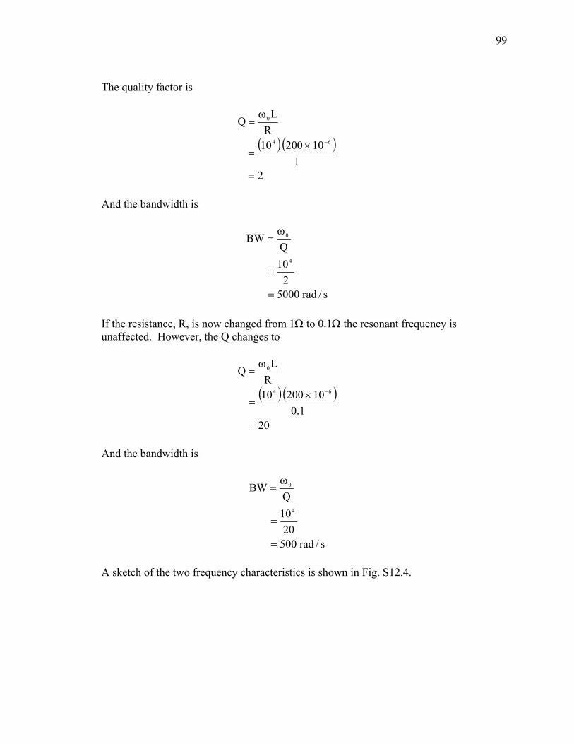
99
The quality factor is
( ) ( )
21
1020010R
LQ
64
0
=
×=
ω=
−
And the bandwidth is
s/rad50002
10Q
BW
4
0
=
=
ω=
If the resistance, R, is now changed from 1Ω to 0.1Ω the resonant frequency is
unaffected. However, the Q changes to
( ) ( )
201.0
1020010R
LQ
64
0
=
×=
ω=
−
And the bandwidth is
s/rad50020
10Q
BW
4
0
=
=
ω=
A sketch of the two frequency characteristics is shown in Fig. S12.4.
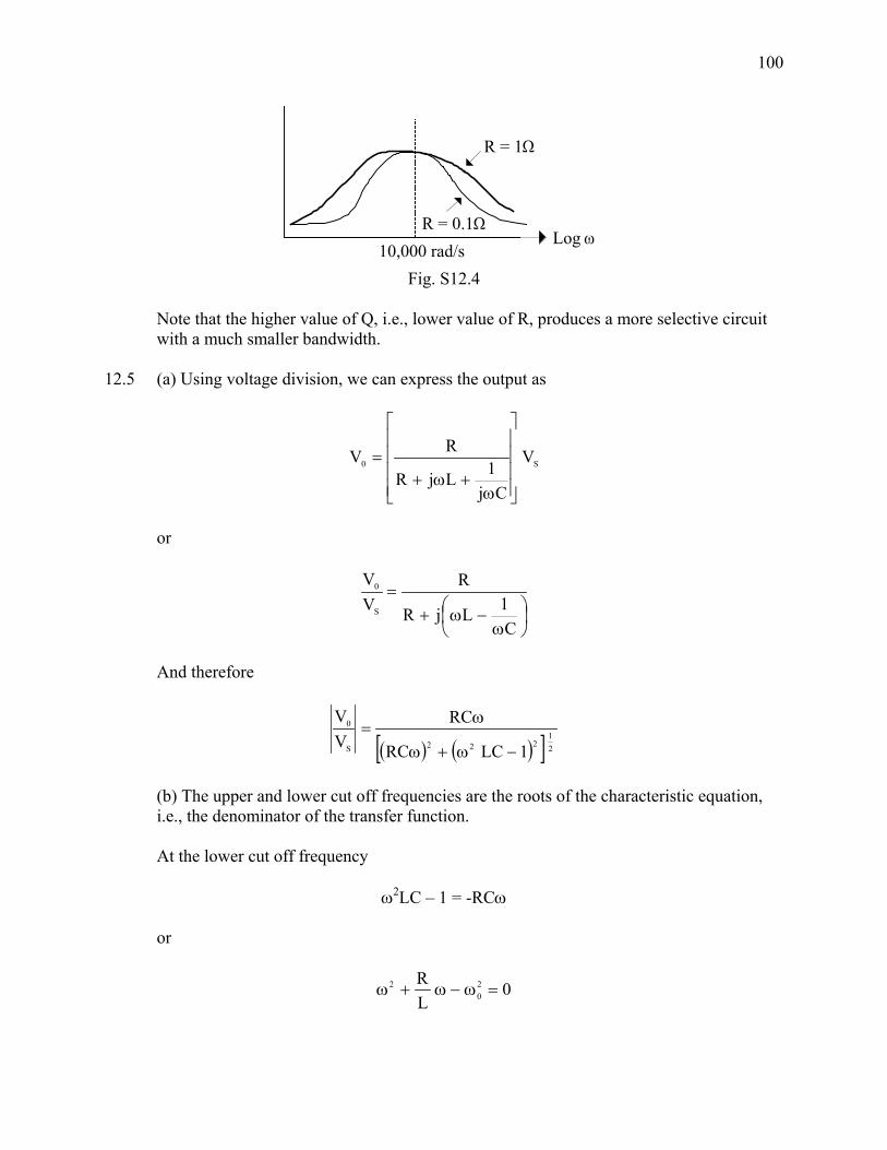
100
Log ω
R = 1Ω
R = 0.1Ω
10,000 rad/s
Fig. S12.4 Note that the higher value of Q, i.e., lower value of R, produces a more selective circuit
with a much smaller bandwidth. 12.5 (a) Using voltage division, we can express the output as
S0 V
Cj1LjR
RV
⎥⎥⎥⎥
⎦
⎤
⎢⎢⎢⎢
⎣
⎡
ω+ω+
=
or
⎟⎠⎞
⎜⎝⎛
ω−ω+
=
C1LjR
RVV
S
0
And therefore
( ) ( )[ ] 21
222S
0
1LCRC
RCVV
−ω+ω
ω=
(b) The upper and lower cut off frequencies are the roots of the characteristic equation,
i.e., the denominator of the transfer function. At the lower cut off frequency
ω2LC – 1 = -RCω or
0LR 2
02 =ω−ω+ω
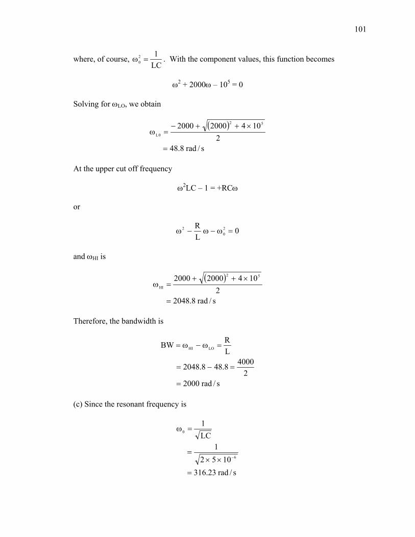
101
where, of course, LC12
0 =ω . With the component values, this function becomes
ω2 + 2000ω – 105 = 0
Solving for ωLO, we obtain
( )
s/rad8.482
10420002000 52
0L
=
×++−=ω
At the upper cut off frequency
ω2LC – 1 = +RCω or
0LR 2
02 =ω−ω−ω
and ωHI is
( )
s/rad8.20482
10420002000 52
HI
=
×++=ω
Therefore, the bandwidth is
s/rad20002
40008.488.2048
LRBW LOHI
=
=−=
=ω−ω=
(c) Since the resonant frequency is
s/rad23.3161052
1LC1
6
0
=
××=
=ω
−
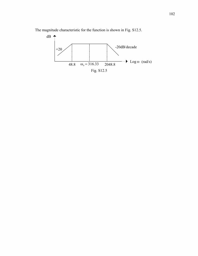
102
The magnitude characteristic for the function is shown in Fig. S12.5.
dB
Log ω48.8 2048.8
-20dB/decade+20
33.3160 =ω (rad/s)
Fig. S12.5

103
CHAPTER 13 PROBLEMS 13.1 If f(t) = e-at sin bt, find F(s) using (a) the definition of the Laplace Transform and (b) the
fact that L[e-at f(t)] = F(s + a). 13.2 Find f(t) if F(s) is given by the expression
( ) ( ) ( ) ( )6s4s2ss24sF
+++=
13.3 Find f(t) if F(s) is given by the expression
( ) ( )( )20s8ss
4s4sF2 ++
+=
13.4 Find f(t) if F(s) is given by the expression
( ) ( )( ) ( )3s1s2s
2s12sF2 +++
+=
13.5 Given the function
( ) ( )( ) ( )4s2ss
10s24sF++
+=
Find the initial and final values of the function by evaluating it in both the s-domain and
time domain.

104
CHAPTER 13 SOLUTIONS 13.1 (a) By definition
( ) ( ) dtetfsF st
0
−∞
∫=
And since f(t) = e-at sin bt
( ) dtebtsinesF st
0
at −∞
−∫=
Using Euler’s identity
( ) ( )
( ) ( )
∫−
=
⎥⎦
⎤⎢⎣
⎡ −∫=
∞ ++−−+−
−∞+−
0
tjbastjbas
jbtjbt
0
tas
dtj2ee
dtj2eeesF
Evaluating the integral
( ) 22 basb
jbas1
jbas1
j21
++=
⎥⎦
⎤⎢⎣
⎡++
−−+
=
(b) In this case f(t) = sin bt. Then
( ) dtbtsinesF0
st∫=∞
−
Again, using the Euler identity
( )
( ) ( )( )∫ −=
⎟⎟⎠
⎞⎜⎜⎝
⎛ −∫=
∞+−−−
−∞−
0
tjbstjbs
jbtjbt
0
ts
dteej2
1
dtj2eeesF
Evaluating the integral
105
22 bsb
jbs1
jbs1
j21
+=
⎥⎦
⎤⎢⎣
⎡+
−−
=
Then using the fact that L[e-at f(t)] = F(s + a) where in this case f(t) = sin bt and
( )22 bs
bsF+
=
we find that
( ) ( )[ ][ ]
( ) 22
at
at
basb
btsinetfeasF
++=
=
=+−
−
LL
13.2 The expression
( ) ( ) ( ) ( )6s4s2ss24sF
+++=
can be written in a partial fraction expansion of the form
( ) ( ) ( ) 6sk
4sk
2sk
6s4s2ss24 321
++
++
+=
+++
Multiplying the entire equation by the term s + 2 yields
( ) ( )( ) ( )
6s2sk
4s2skk
6s4ss24 32
1 ++
++
++=
++
If we now evaluate each term at s = -2, we find that the last two terms on the right side of
the equation vanish and we have
( ) ( )
1
1
2s
k6
k6s4s
s24
=−
=++
−=
Repeating this procedure for the two remaining terms in the denominator, i.e., (s + 4) and
(s + 6) yields
106
( ) ( )
2
2
4s
k24
k6s2s
s24
=
=++
−=
And
( ) ( )3
3
6s
k18
k4s2s
s24
=−
=++
−=
Now the function F(s) can be written in the form
( )6s
184s
242s
6sF+
−+
++
−=
The reader can check the validity of this expansion by recombining the terms to produce
the original expression. Once F(s) is in this latter form, we can use the transform pair
[ ]as
1e at
+=−L
And hence
( ) [ ] ( )tue18e24e6tf t6t4t2 −−− −+−= 13.3 We begin by writing the function in a partial fraction expansion. Therefore, we need to
know the roots of the quadratic term. We can either employ the quadratic formula or recognize that
s2 + 8s + 20 = s2 + 8s + 16 + 4
= (s + 4)2 + 4 = (s + 4 – j2) (s + 4 + j2) Hence, the function F(s) can be written as
( ) ( )( ) ( ) 2j4s
k2j4s
ks
k2j4s2j4ss
4s4sF*110
+++
−++=
++−++
=
Multiplying the entire equation by s and evaluating it at s = 0 yields
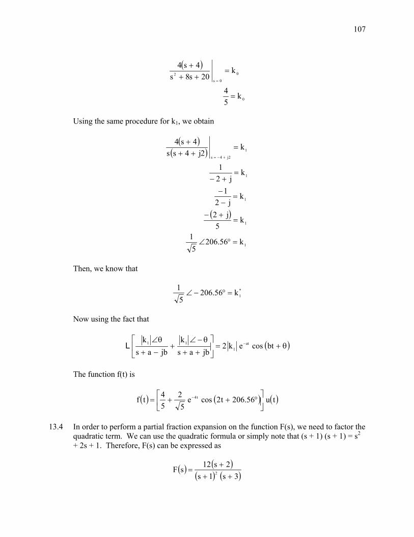
107
( )
0
0
0s2
k54
k20s8s
4s4
=
=++
+
=
Using the same procedure for k1, we obtain
( )( )
( )
1
1
1
1
1
2j4s
k56.2065
1
k5
j2
kj2
1
kj2
1
k2j4ss
4s4
=°∠
=+−
=−
−
=+−
=++
+
+−=
Then, we know that
*1k56.206
51
=°−∠
Now using the fact that
( )θ+=⎥⎦
⎤⎢⎣
⎡
++
θ−∠+
−+
θ∠− btcosek2
jbask
jbask at
111L
The function f(t) is
( ) ( ) ( )tu56.206t2cose5
254tf t4
⎥⎦
⎤⎢⎣
⎡°++= −
13.4 In order to perform a partial fraction expansion on the function F(s), we need to factor the
quadratic term. We can use the quadratic formula or simply note that (s + 1) (s + 1) = s2 + 2s + 1. Therefore, F(s) can be expressed as
( ) ( )( ) ( )3s1s
2s12sF 2 +++
=
108
or in the form
( ) ( )( ) ( ) ( ) 3s
k1s
k1s
k3s1s
2s12sF 22
12112 +
++
++
=++
+=
If we now multiply the entire equation by (s + 1)2, we obtain
( ) ( ) ( )3s1skk1sk
3s2s12 2
21211 +
++++=
++
Now evaluating this equation at s = -1 yields
( )
12
12
1s
k6
k3s
2s12
=
=++
−=
In order to evaluate k11 we differentiate each term of the equation with respect to s and
evaluate all terms at s = -1. Note that the derivative of k12 with respect to s is zero, the derivative of the last term in the equation with respect to s will still have an (s + 1) term in the numerator that will vanish when evaluated at s = -1, and the derivative of the first term on the right side of the equation with respect to s simply yields k11. Therefore,
( )
( ) ( ) ( ) ( )( )
11
11
1s
2
11
1s
k3
k3s
12s12123s
k3s
2s12dsd
=
=+
+−+
=⎥⎦
⎤⎢⎣
⎡++
−=
−=
Finally,
( )( )
2
2
3s
2
k3
k1s
2s12
=−
=+
+
−=
And therefore, F(s) can be expressed in the form
( )( ) 2s
31s
61s
3sF 2 +−
++
+=
109
Using the transform pairs, we find that
( ) [ ] ( )tue3te6e3tf t2tt −−− −+= 13.5 First, let us use the Theorems to evaluate the function in the s-domain. The initial value can be derived from the Theorem
lim f(t) = lim sF(s) t → 0 s → ∞ Therefore,
( ) ( )( ) ( )
0s8
s61
s240
s24
slim
8s6s240s24
slim
4s2s10s24
slim
ssFlim
2
2
2
=⎥⎥⎥⎥
⎦
⎤
⎢⎢⎢⎢
⎣
⎡
++
+
∞→=
⎥⎦
⎤⎢⎣
⎡++
+∞→
=
⎥⎦
⎤⎢⎣
⎡++
+∞→
=
The final value is derived from the expression
lim f(t) = lim sF(s) t → ∞ s → 0 Hence,
( ) ( )( ) ( )
308
2404s2s
10s240s
lim0sssFlim
=
=
⎥⎦
⎤⎢⎣
⎡++
+→
=→
The time function can be derived from a partial fraction expansion as
( ) ( )( ) ( ) 4s
k2s
ks
k4s2ss
10s24sF 210
++
++=
+++
=
where

110
( )
( ) ( )( )( )( )( ) 18k
2ss10s24
48k4ss10s24
30k4s2s
10s24
2
4s
1
2s
0
0s
==++
−==++
==++
+
−=
−=
=
Hence,
( )4s
182s
48s
30sF+
++
−=
and then
( ) [ ] ( )tue18e4830tf t4t2 −− +−= Given this expression, we find that
( ) [ ] 01848300ttflim
=+−=→
and
( ) [ ] 300030t
tflim=+−=
∞→
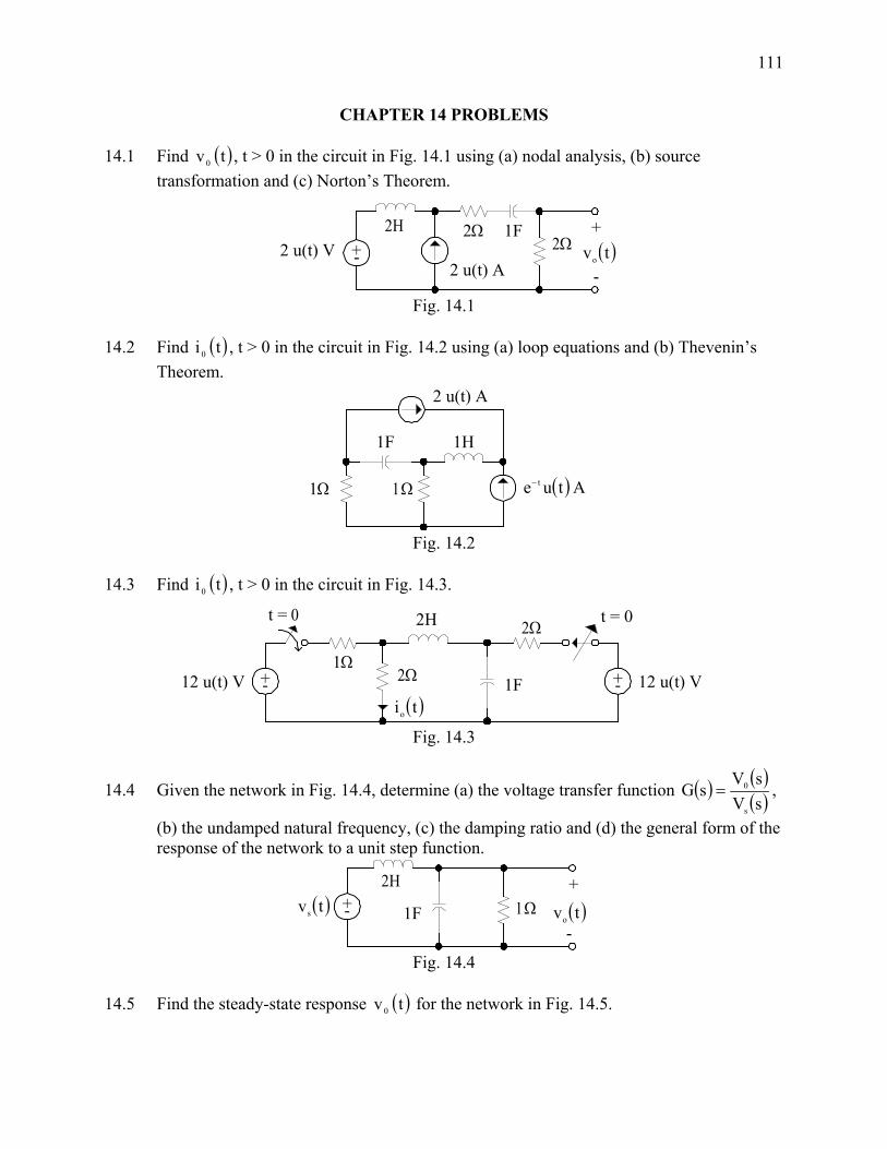
111
CHAPTER 14 PROBLEMS 14.1 Find ( )tv0 , t > 0 in the circuit in Fig. 14.1 using (a) nodal analysis, (b) source
transformation and (c) Norton’s Theorem.
2Ω2Η 2Ω
+-
+2 u(t) V
1F
-( )tvo
2 u(t) A
Fig. 14.1 14.2 Find ( )ti 0 , t > 0 in the circuit in Fig. 14.2 using (a) loop equations and (b) Thevenin’s
Theorem.
1Ω1Ω
1F
( ) Atue t−
2 u(t) A
1H
Fig. 14.2
14.3 Find ( )ti 0 , t > 0 in the circuit in Fig. 14.3.
2Ω
t = 0
1Ω+-12 u(t) V 1F
t = 0
12 u(t) V( )tio
+-
2Ω2H
Fig. 14.3
14.4 Given the network in Fig. 14.4, determine (a) the voltage transfer function ( ) ( )( )sVsV
sGs
0= ,
(b) the undamped natural frequency, (c) the damping ratio and (d) the general form of the response of the network to a unit step function.
1Ω
2Η+-
+
1F-( )tvo
( )tvs
Fig. 14.4
14.5 Find the steady-state response ( )tv0 for the network in Fig. 14.5.
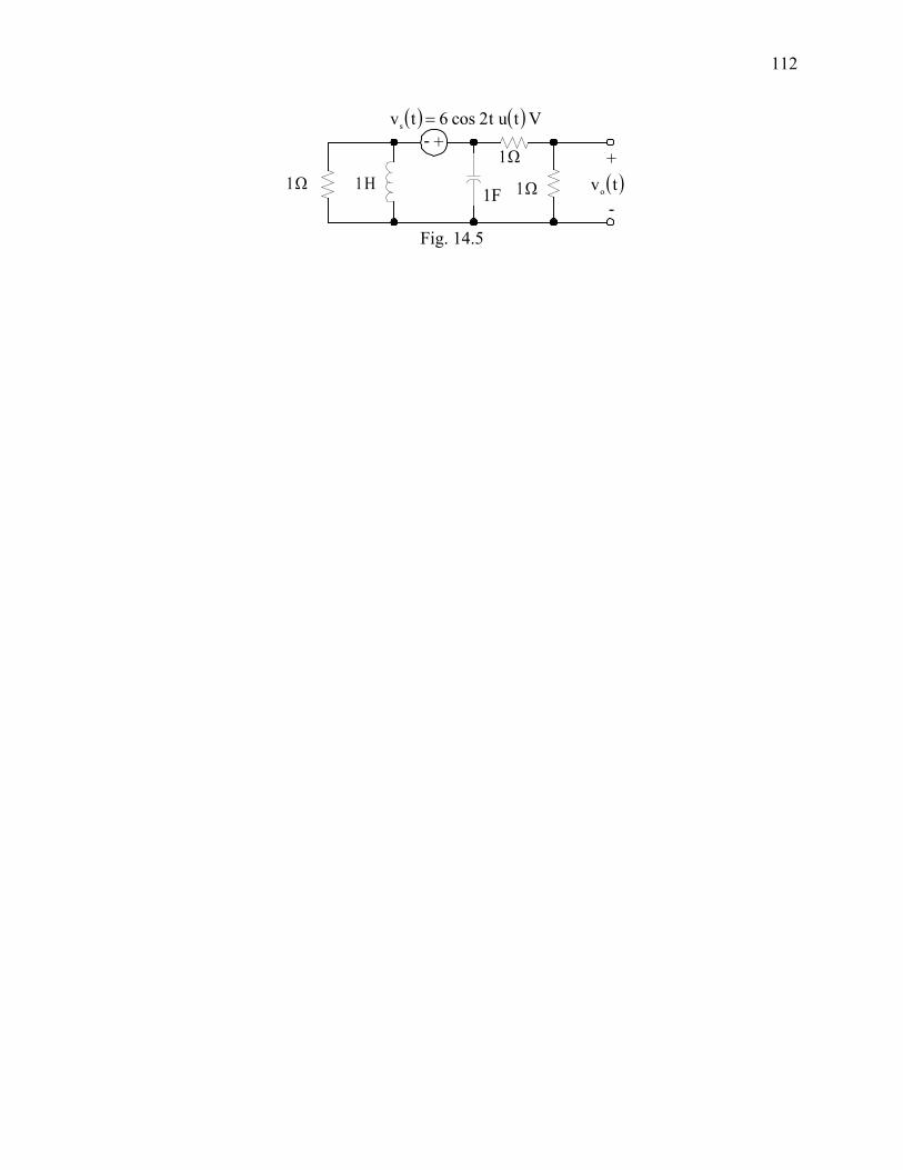
112
1Ω1Η
+-+
1F-( )tvo
( ) ( ) Vtut2cos6tvs =
1Ω1Ω
Fig. 14.5
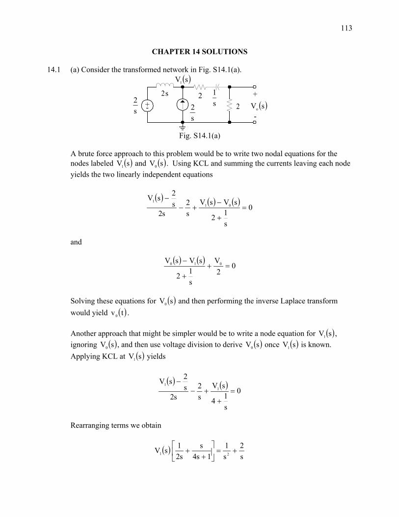
113
CHAPTER 14 SOLUTIONS 14.1 (a) Consider the transformed network in Fig. S14.1(a).
2
2s 2+-
+
-( )sVo
s1
s2s
2
( )sV1
Fig. S14.1(a)
A brute force approach to this problem would be to write two nodal equations for the
nodes labeled ( )sV1 and ( )sV0 . Using KCL and summing the currents leaving each node yields the two linearly independent equations
( ) ( ) ( )0
s12
sVsVs2
s2s2sV
011
=+
−+−
−
and
( ) ( )0
2V
s12
sVsV 010 =++
−
Solving these equations for ( )sV0 and then performing the inverse Laplace transform
would yield ( )tv0 . Another approach that might be simpler would be to write a node equation for ( )sV1 ,
ignoring ( )sV0 , and then use voltage division to derive ( )sV0 once ( )sV1 is known. Applying KCL at ( )sV1 yields
( ) ( )0
s14
sVs2
s2s2sV
11
=+
+−−
Rearranging terms we obtain
( )s2
s1
1s4s
s21sV
21 +=⎥⎦
⎤⎢⎣
⎡+
+

114
or
( ) ( ) 2
2
1 s1s2
1s4s21s4s2sV +
=⎥⎦
⎤⎢⎣
⎡+
++
Solving for ( )sV1 yields
( ) ( ) ( )( )1s4s2s
1s41s22sV21 ++
++=
Now applying voltage division
( ) ( )
( )1s4s2
1s24s14
2sVsV
2
10
+++
=
⎟⎟⎟⎟
⎠
⎞
⎜⎜⎜⎜
⎝
⎛
+=
This function can be written in partial fraction expansion form as
71.1sB
29.0sA
21s2s
2s42 +
++
=++
+
where
59.071.1s2s4A
29.0s
=+
+=
−=
and
41.329.0s2s4B
71.1s
=+
+=
−=
Therefore,
( ) [ ] ( ) Vtue41.3e59.0tv t71.1t29.00
−− +=
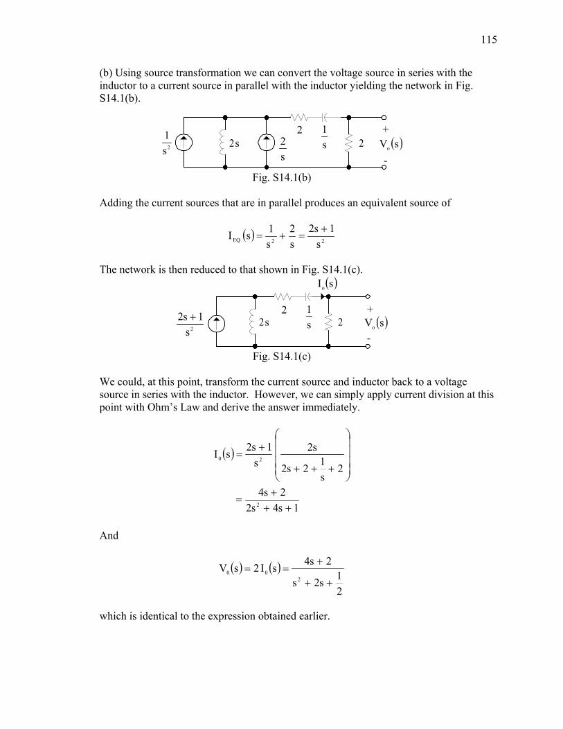
115
(b) Using source transformation we can convert the voltage source in series with the inductor to a current source in parallel with the inductor yielding the network in Fig. S14.1(b).
22s2 +
-( )sVos
1
s2
2s1
Fig. S14.1(b)
Adding the current sources that are in parallel produces an equivalent source of
( )22EQ s
1s2s2
s1sI +
=+=
The network is then reduced to that shown in Fig. S14.1(c).
22s2 +
-( )sVos
12s
1s2 +
( )sIo
Fig. S14.1(c)
We could, at this point, transform the current source and inductor back to a voltage
source in series with the inductor. However, we can simply apply current division at this point with Ohm’s Law and derive the answer immediately.
( )
1s4s22s4
2s12s2
s2s
1s2sI
2
20
+++
=
⎟⎟⎟⎟
⎠
⎞
⎜⎜⎜⎜
⎝
⎛
+++
+=
And
( ) ( )
21s2s
2s4sI2sV2
00
++
+==
which is identical to the expression obtained earlier.
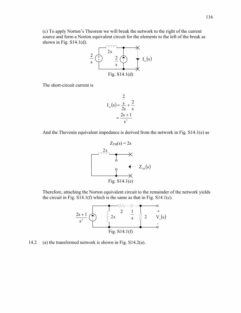
116
(c) To apply Norton’s Theorem we will break the network to the right of the current source and form a Norton equivalent circuit for the elements to the left of the break as shown in Fig. S14.1(d).
2s
s2 ( )sIsc
+-s2
Fig. S14.1(d)
The short-circuit current is
( )
2
sc
s1s2s2
s2s2
sI
+=
+=
And the Thevenin equivalent impedance is derived from the network in Fig. S14.1(e) as
ZTH(s) = 2s 2s
( )sZTH
Fig. S14.1(e)
Therefore, attaching the Norton equivalent circuit to the remainder of the network yields
the circuit in Fig. S14.1(f) which is the same as that in Fig. S14.1(c).
22s2 +
-( )sVos
12s
1s2 +
Fig. S14.1(f)
14.2 (a) the transformed network is shown in Fig. S14.2(a).
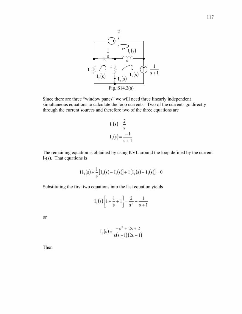
117
11 1s
1+
ss1
s2
( )sI1
( )sI3( )sI2 ( )sI0
Fig. S14.2(a) Since there are three “window panes” we will need three linearly independent
simultaneous equations to calculate the loop currents. Two of the currents go directly through the current sources and therefore two of the three equations are
( )
( )1s
1sI
s2sI
3
1
+−
=
=
The remaining equation is obtained by using KVL around the loop defined by the current
I2(s). That equations is
( ) ( ) ( )[ ] ( ) ( )[ ] 0sIsI1sIsIs1sI1 32122 =−+−+
Substituting the first two equations into the last equation yields
( )1s
1s21
s11sI
22 +−=⎥⎦
⎤⎢⎣⎡ ++
or
( ) ( ) ( )1s21ss2s2ssI
2
2 ++++−
=
Then
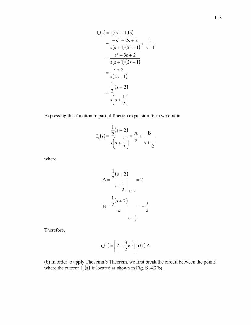
118
( ) ( ) ( )
( ) ( )
( ) ( )
( )
( )
⎟⎠⎞
⎜⎝⎛ +
+=
++
=
++++
=
++
++++−
=
−=
21ss
2s21
1s2s2s
1s21ss2s3s
1s1
1s21ss2s2s
sIsIsI
2
2
320
Expressing this function in partial fraction expansion form we obtain
( )( )
21s
BsA
21ss
2s21
sI0
++=
⎟⎠⎞
⎜⎝⎛ +
+=
where
( )
( )23
s
2s21
B
2
21s
2s21
A
21s
0s
−=+
=
=+
+=
−=
=
Therefore,
( ) ( ) Atue232ti 2
t
0 ⎥⎦
⎤⎢⎣
⎡ −=−
(b) In order to apply Thevenin’s Theorem, we first break the circuit between the points
where the current ( )sI0 is located as shown in Fig. S14.2(b).
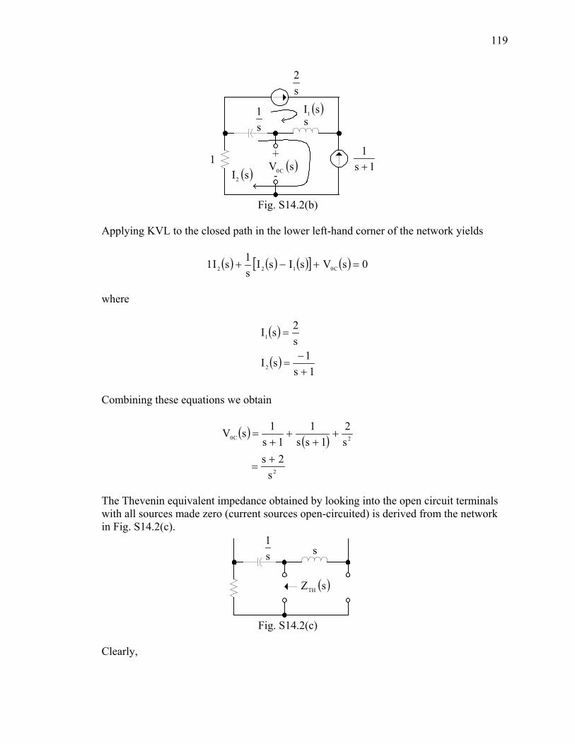
119
1 1s1+
ss1
s2
( )sI1
( )sI2
( )sV C0
+
-
Fig. S14.2(b)
Applying KVL to the closed path in the lower left-hand corner of the network yields
( ) ( ) ( )[ ] ( ) 0sVsIsIs1sI1 C0122 =+−+
where
( )
( )1s
1sI
s2sI
2
1
+−
=
=
Combining these equations we obtain
( ) ( )
2
2C0
s2s
s2
1ss1
1s1sV
+=
++
++
=
The Thevenin equivalent impedance obtained by looking into the open circuit terminals
with all sources made zero (current sources open-circuited) is derived from the network in Fig. S14.2(c).
ss1
( )sZTH
Fig. S14.2(c)
Clearly,
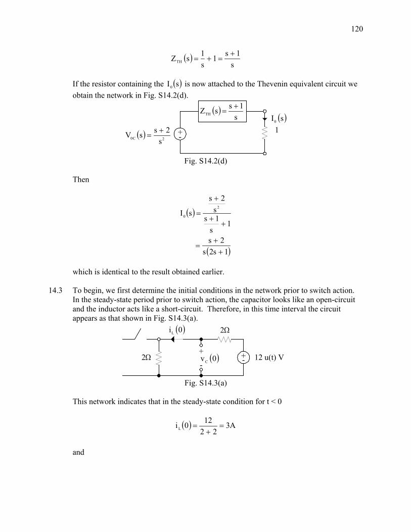
120
( )s
1s1s1sZTH
+=+=
If the resistor containing the ( )sI0 is now attached to the Thevenin equivalent circuit we
obtain the network in Fig. S14.2(d).
1( )2C0 s2ssV +
=
( )s
1ssZTH
+=
+-
( )sI0
Fig. S14.2(d)
Then
( )
( )1s2s2s
1s
1ss
2s
sI2
0
++
=
++
+
=
which is identical to the result obtained earlier. 14.3 To begin, we first determine the initial conditions in the network prior to switch action.
In the steady-state period prior to switch action, the capacitor looks like an open-circuit and the inductor acts like a short-circuit. Therefore, in this time interval the circuit appears as that shown in Fig. S14.3(a).
2Ω
2Ω
+-+
-( )0vC
( )0iL
12 u(t) V
Fig. S14.3(a)
This network indicates that in the steady-state condition for t < 0
( ) A322
120iL =+
=
and
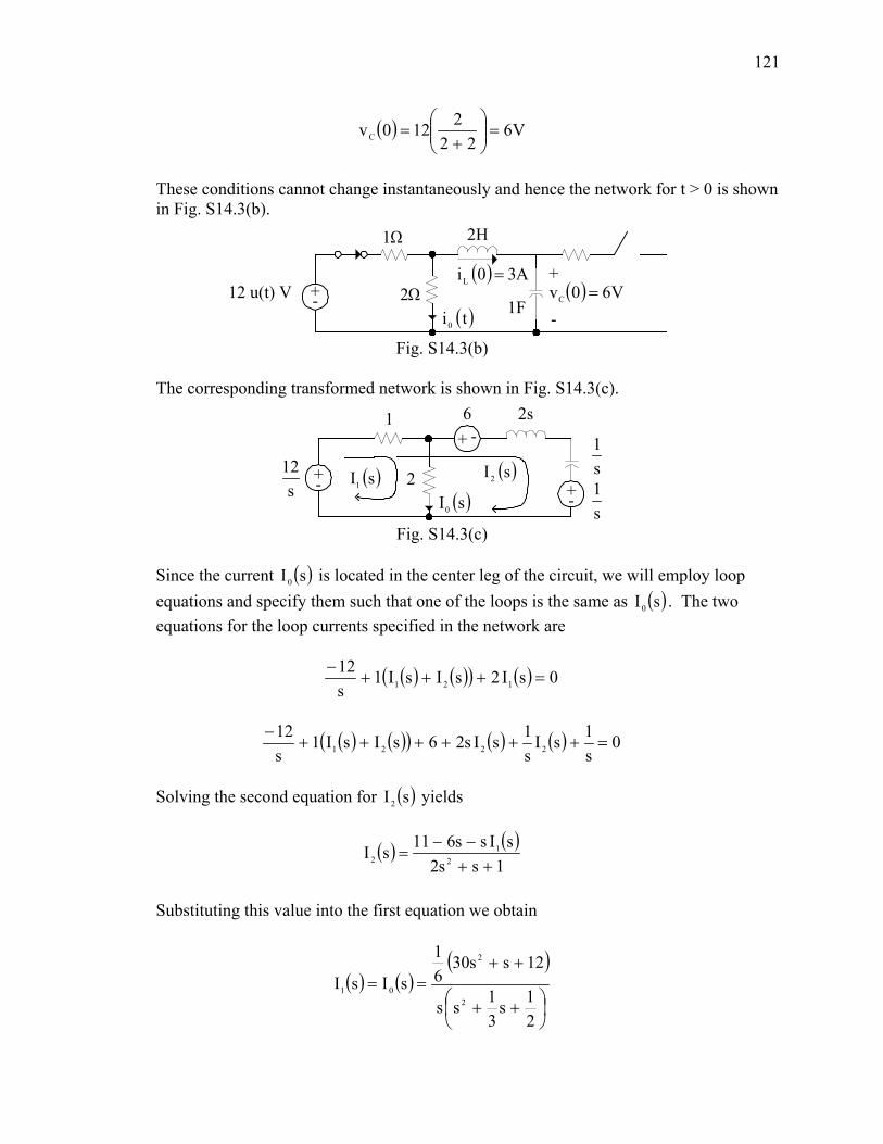
121
( ) V622
2120vC =⎟⎟⎠
⎞⎜⎜⎝
⎛+
=
These conditions cannot change instantaneously and hence the network for t > 0 is shown
in Fig. S14.3(b).
1F2Ω
1Ω
+
-( ) V60vC =
( ) A30iL =
( )ti0
2H
12 u(t) V +-
Fig. S14.3(b)
The corresponding transformed network is shown in Fig. S14.3(c).
2
1
( )sI2
( )sI0
2s
+-
+ -
s12
6
+-
s1
s1( )sI1
Fig. S14.3(c)
Since the current ( )sI0 is located in the center leg of the circuit, we will employ loop
equations and specify them such that one of the loops is the same as ( )sI0 . The two equations for the loop currents specified in the network are
( ) ( )( ) ( ) 0sI2sIsI1s12
121 =+++−
( ) ( )( ) ( ) ( ) 0s1sI
s1sIs26sIsI1
s12
2221 =++++++−
Solving the second equation for ( )sI2 yields
( ) ( )1ss2
sIss611sI
21
2 ++−−
=
Substituting this value into the first equation we obtain
( ) ( )( )
⎟⎠⎞
⎜⎝⎛ ++
++==
21s
31ss
12ss3061
sIsI2
2
01
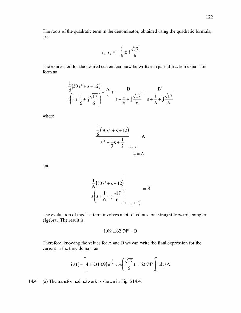
122
The roots of the quadratic term in the denominator, obtained using the quadratic formula, are
617j
61s,s 21 ±−=
The expression for the desired current can now be written in partial fraction expansion
form as
( )
617j
61s
B
617j
61s
BsA
617j
61ss
12ss3061
*2
+++
+−+=
⎟⎟⎠
⎞⎜⎜⎝
⎛±+
++
where
( )
A4
A
21s
31s
12ss3061
0s
2
2
=
=++
++
=
and
( )B
617j
61ss
12ss3061
617j
61s
2
=
⎟⎟⎠
⎞⎜⎜⎝
⎛++
++
+−=
The evaluation of this last term involves a lot of tedious, but straight forward, complex
algebra. The result is
B74.6209.1 =°∠ Therefore, knowing the values for A and B we can write the final expression for the
current in the time domain as
( ) ( ) ( ) Atu74.62t617cose09.124ti 6
t
0⎥⎥⎦
⎤
⎢⎢⎣
⎡⎟⎟⎠
⎞⎜⎜⎝
⎛°++=
−
14.4 (a) The transformed network is shown in Fig. S14.4.
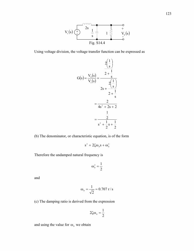
123
1 ( )sV0
2s+-
+
-s1( )sVs
Fig. S14.4
Using voltage division, the voltage transfer function can be expressed as
( ) ( )( )
21s
21s
21
2s2s42
s12
s12
s2
s12
s12
sVsV
sG
2
2
s
0
++=
++=
+
⎟⎠⎞
⎜⎝⎛
+
+
⎟⎠⎞
⎜⎝⎛
==
(b) The denominator, or characteristic equation, is of the form
200
2 s2s ω+ζω+ Therefore the undamped natural frequency is
212
0 =ω
and
s/r707.02
10 ==ω
(c) The damping ratio is derived from the expression
212 0 =ζω
and using the value for 0ω we obtain
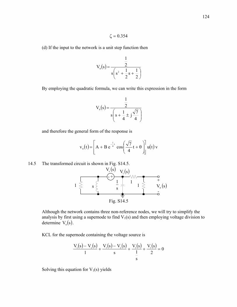
124
354.0=ζ
(d) If the input to the network is a unit step function then
( )⎟⎠⎞
⎜⎝⎛ ++
=
21s
21ss
21
sV2
0
By employing the quadratic formula, we can write this expression in the form
( )
⎟⎟⎠
⎞⎜⎜⎝
⎛±+
=
47j
41ss
21
sV0
and therefore the general form of the response is
( ) ( ) vtut47coseBAtv
t41
0⎥⎥⎦
⎤
⎢⎢⎣
⎡⎟⎟⎠
⎞⎜⎜⎝
⎛θ++=
−
14.5 The transformed circuit is shown in Fig. S14.5.
1 ( )sV0s+
-s1
( )sVs
1- +
1
( )sV1
Fig. S14.5
Although the network contains three non-reference nodes, we will try to simplify the
analysis by first using a supernode to find V1(s) and then employing voltage division to determine ( )sV0 .
KCL for the supernode containing the voltage source is
( ) ( ) ( ) ( ) ( ) ( )0
2sV
s1
sVs
sVsV1
sVsV 11s1s1 =++−
+−
Solving this equation for V1(s) yields
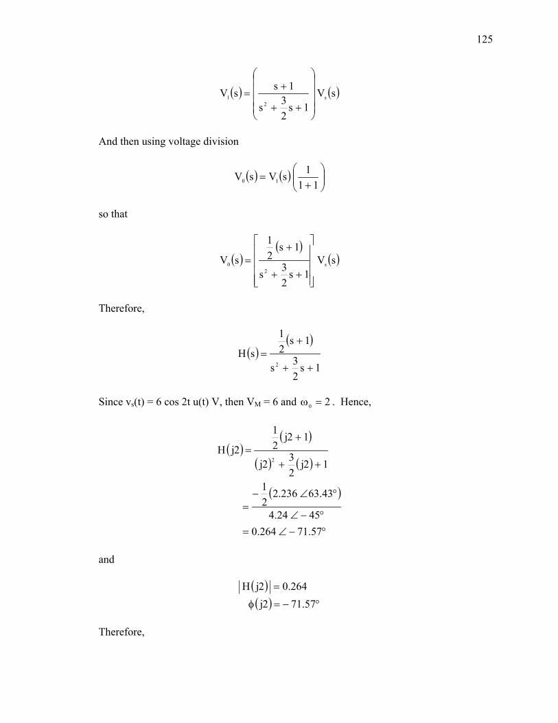
125
( ) ( )sV1s
23s
1ssV s2
1
⎟⎟⎟⎟
⎠
⎞
⎜⎜⎜⎜
⎝
⎛
++
+=
And then using voltage division
( ) ( ) ⎟⎟⎠
⎞⎜⎜⎝
⎛+
=11
1sVsV 10
so that
( )( )
( )sV1s
23s
1s21
sV s2
0
⎥⎥⎥⎥
⎦
⎤
⎢⎢⎢⎢
⎣
⎡
++
+=
Therefore,
( )( )
1s23s
1s21
sH2 ++
+=
Since vs(t) = 6 cos 2t u(t) V, then VM = 6 and 20 =ω . Hence,
( )( )
( ) ( )
( )
°−∠=°−∠
°∠−=
++
+=
57.71264.04524.4
43.63236.221
12j232j
12j21
2jH2
and
( )( ) °−=φ
=
57.712j264.02jH
Therefore,
126
( ) ( ) ( )( )( ) V57.71t2cos58.1
2jt2cos2jHVtv Mss0
°−=
φ+=
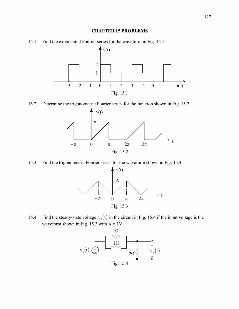
127
CHAPTER 15 PROBLEMS 15.1 Find the exponential Fourier series for the waveform in Fig. 15.1.
-3 -2 -1
1
2
v(t)
t(s)543210
Fig. 15.1 15.2 Determine the trigonometric Fourier series for the function shown in Fig. 15.2.
v(t)
0 t
π
π− π π2 π3
Fig. 15.2 15.3 Find the trigonometric Fourier series for the waveform shown in Fig. 15.3.
v(t)
0t
π− π π2
A
Fig. 15.3
15.4 Find the steady-state voltage ( )tv0 in the circuit in Fig. 15.4 if the input voltage is the
waveform shown in Fig. 15.3 with A = 1V.
1H( )tv02Ω
+-+
-( )tvs
1Ω
Fig. 15.4
128
15.5 Given the network in Fig. 15.4 with the input source ( ) ( ) Vtue10tv t2s
−= , use the transform technique to find ( )tv0 .
129
CHAPTER 15 SOLUTIONS
15.1 An examination of the waveform indicates that the period T = 3 and 3
2T2
0
π=
π=ω .
The Fourier coefficients are determined from the expression
( ) dtetvT1c tjn
T
0n
0ω−∫=
or in this case
[ ]( )[ ]
[ ]
⎟⎟⎠
⎞⎜⎜⎝
⎛⎟⎠⎞
⎜⎝⎛ π
−π
=
⎥⎥⎥
⎦
⎤
⎢⎢⎢
⎣
⎡
⎟⎟⎟
⎠
⎞
⎜⎜⎜
⎝
⎛ +−
π=
⎟⎟⎠
⎞⎜⎜⎝
⎛⎟⎠
⎞⎜⎝
⎛ +−π
=
⎥⎦
⎤⎢⎣
⎡ −+π
−=
−+ω
−=
−+−ω
−=
+ω
−=
⎥⎦⎤
⎢⎣⎡ ∫+∫=
π−
π−π
π−
π−π−
π−π−
ω−ω−
ω−ω−ω−
ω−ω−
ω−ω−
3ncose1
jn1
2eee22
n2j1
ee2n2j
1
2een2j
1
2eejn3
1
ee1e2jn3
1
ee2jn3
1
dte1dte231c
jn
3jn
3jn
nj
3n4j
3n2j
3n4j
3n2j
n2jjn
0
jnn2jjn
0
2
1
tjn1
0
tjn
0
tjn2
1
tjn1
0n
00
000
00
00
In addition
( )
1
dt1dt231
dttvT1c
2
1
1
0
3
00
=
⎥⎦⎤
⎢⎣⎡ ∫+∫=
∫=
Therefore,
130
( ) tjnjn
0nn
0e3
ncose1jn11tv ωπ−
∞
≠∞−=
⎟⎟⎠
⎞⎜⎜⎝
⎛⎟⎠⎞
⎜⎝⎛ π
−∑π
+=
15.2 Since the waveform does not exhibit any symmetry, we will have to determine the
coefficients nn0 banda,a . The 0a coefficient is
( ) dttv21a 0 ∫π
=π
π−
where, of course, v(t) = t in the interval π≤≤ t0 and zero elsewhere and 1T2
0 =π
=ω .
⎟⎟⎠
⎞⎜⎜⎝
⎛ π=
π=
∫π
=
π
π
42t
21
dtt21a
0
2
00
Recall that 0a is simply the average value of the waveform and therefore can be
calculated by dividing the area under the curve ( ( ) ( )22
1bh21Area
2π=ππ== ) by the
interval (2π) which yields 4π .
The an coefficient is
dtntcost22a
0n ∫
π=
π
Using a table of integrals, we find that
π
⎥⎦⎤
⎢⎣⎡ +
π=
02n ntsint
n1ntcos
n11a
The second term is zero at t = π and 0 and the first term can be written as
( )[ ]11n1a n
2n −−π
=
since the cosine term will be +1 or –1 depending upon the value of n. Thus
131
( )2
n
n n11a
π−−
=
In addition,
dttsint22b
0n ∫
π=
π
Once again, using a set of integral tables we find that
π
⎥⎦⎤
⎢⎣⎡ −
π=
02n ntcost
n1ntsin
n11b
The first term will be zero at each limit, but the second term is nonzero at the upper limit
and thus
( )
( )n
1
1n
b
n
nn
−−=
−ππ−
=
Therefore, the Fourier series expansion is
( ) ( ) ( ) ntsinn1ntcos
n11
4tv
n
1n2
n −−∑ ⎥
⎦
⎤⎢⎣
⎡π
−−+
π=
∞
=
15.3 To begin our analysis we first note that the waveform is an even function and therefore
0bn = for all n. Thus, we need to find only the 0a and an coefficients.
For this waveform, we note that T = 2π and 1T2
0 =π
=ω . 0a is now
( ) dttv21a 0 ∫π
=π
π−
However, recall that 0a is simply the average value and we can easily compute this
number without resorting to solving the above integral. This average value can be obtained by dividing the area by the base, i.e.
( ) AA212bh
212Area π=⎟
⎠⎞
⎜⎝⎛ π=⎟
⎠⎞
⎜⎝⎛=
132
The base is 2π and therefore
2A
2Aa 0 =π
π=
Because the function is even,
dtntcostA24a
0n ∫
ππ=
π
where the equation of the straight line function in the interval π≤≤ t0 is tAπ
. So,
dtntcostA2a0
2n ∫π
=π
Using a table of integrals, we find that
( )
( )( )
( )evennfor0
oddnfornA4
1ncosnA2
1ncosn1A2
ntsintn1ntcos
n1A2a
2
2
22
022n
=π−
=
−ππ
=
⎥⎦⎤
⎢⎣⎡ −π
π=
⎥⎦⎤
⎢⎣⎡ +
π=
π
Therefore,
( )( )
ntcosnA4
2Atv
oddn1n
2∑π−
+=∞
=
15.4 The input voltage for the circuit in Fig. 14.4 is given by the expression
( )( )
ntcosn4
21tv
oddn1n
2s ∑π−
+=∞
=
where 10 =ω . The output voltage for the network can be derived using voltage division
as
133
( ) ( ) ( ) ( )
( ) ( )ω⎥⎦
⎤⎢⎣
⎡ω+ω+
=
ω
ω+ω
+=ω
jVj32j12
jV
j1j12
2jV
s
s0
and since 10 =ω
( ) ( ) ( )nVjn32jn12nV s0 ⎥
⎦
⎤⎢⎣
⎡+
+=
Since ( )21dcVs =
( )
21
21
22dcV0
=
⎟⎠⎞
⎜⎝⎛
⎟⎠⎞
⎜⎝⎛=
Furthermore,
( ) ( )
( ) ( )
( ) ( )
( ) ( )°∠×=⎥
⎦
⎤⎢⎣
⎡++
π−
=ω
°∠×=⎥⎦
⎤⎢⎣
⎡++
π−
=ω
°∠×=⎥⎦
⎤⎢⎣
⎡++
π−
=ω
°∠=⎥⎦
⎤⎢⎣
⎡+
+π−
=ω
−
−
−
31.1771054.521j27j12
4947V
28.1761009.115j2
5j1225
45V
09.1741009.39j23j12
943V
69.168318.0j32j124V
3200
2200
2200
200
Hence,
( ) ( ) ( )
( ) ( ) …+°+×+°+×+
°+×+°++=
−−
−
31.177t7cos1054.528.176t5cos1009.1
09.174t3cos1009.369.168tcos318.021tv
32
20
15.5 The input function to the network can be expressed in the form
134
( )2j
10jVs +ω=ω
The transfer function for the network obtained in the previous problem is
( ) ( )ω+ω+
=ωj32j12jG
Then using the time convolution property of the Fourier transform we can express the
output of the circuit in the form
( ) ( ) ( )( )
( )
( ) ⎟⎠⎞
⎜⎝⎛ +ω+ω
+ω=
⎥⎦
⎤⎢⎣
⎡ω+⎥
⎦
⎤⎢⎣
⎡ω+ω+
=
ωω=ω
32j2j
1j3
20j2
10j32j12
jVjGjV s0
which can be written as a partial fraction expansion of the form
( )
( )32j
B2j
A
32j2j
1j3
20
+ω+
+ω=
⎟⎠⎞
⎜⎝⎛ +ω+ω
+ω
Evaluating the constants yields
( )
( )( ) 3
5B2j
1j320
5A
32j
1j320
32
j
2j
==+ω
+ω
==⎟⎠⎞
⎜⎝⎛ +ω
+ω
−=ω
−=ω
Therefore,
135
( )
32j
35
2j5jV0
+ω+
+ω=ω
And
( ) ( ) Vtue35e5tv
t32
t20 ⎥
⎦
⎤⎢⎣
⎡+=
−−
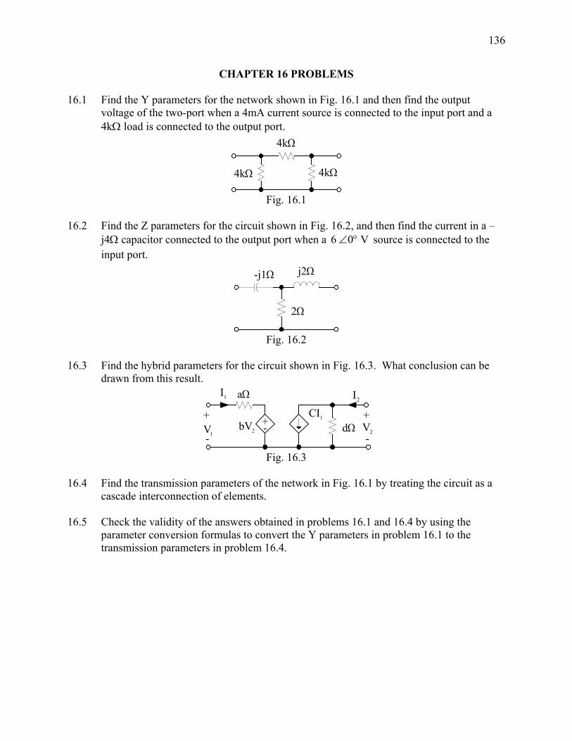
136
CHAPTER 16 PROBLEMS 16.1 Find the Y parameters for the network shown in Fig. 16.1 and then find the output
voltage of the two-port when a 4mA current source is connected to the input port and a 4kΩ load is connected to the output port.
4kΩ 4kΩ
4kΩ
Fig. 16.1
16.2 Find the Z parameters for the circuit shown in Fig. 16.2, and then find the current in a –
j4Ω capacitor connected to the output port when a V06 °∠ source is connected to the input port.
2Ω
j2Ω-j1Ω
Fig. 16.2
16.3 Find the hybrid parameters for the circuit shown in Fig. 16.3. What conclusion can be
drawn from this result.
2V+
-2bV +-
1V+
-
1CI2I1I aΩ
dΩ
Fig. 16.3
16.4 Find the transmission parameters of the network in Fig. 16.1 by treating the circuit as a
cascade interconnection of elements. 16.5 Check the validity of the answers obtained in problems 16.1 and 16.4 by using the
parameter conversion formulas to convert the Y parameters in problem 16.1 to the transmission parameters in problem 16.4.
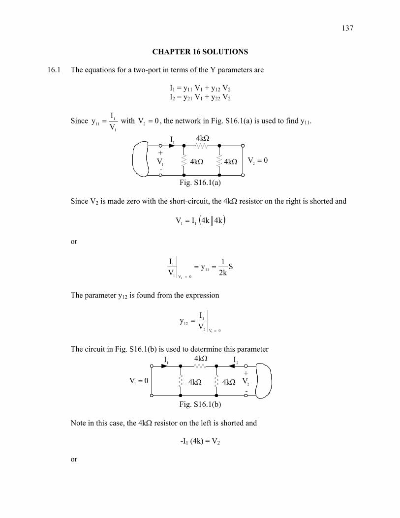
137
CHAPTER 16 SOLUTIONS 16.1 The equations for a two-port in terms of the Y parameters are
I1 = y11 V1 + y12 V2 I2 = y21 V1 + y22 V2
Since 1
111 V
Iy = with 0V2 = , the network in Fig. S16.1(a) is used to find y11.
1V+
-
1I
0V2 =4kΩ4kΩ
4kΩ
Fig. S16.1(a)
Since V2 is made zero with the short-circuit, the 4kΩ resistor on the right is shorted and
( )k4k4IV 11 = or
Sk21y
VI
11
0V1
1
2
===
The parameter y12 is found from the expression
0V2
112
1VI
y=
=
The circuit in Fig. S16.1(b) is used to determine this parameter
2V+
-
1I
0V1 = 4kΩ4kΩ
4kΩ2I
Fig. S16.1(b)
Note in this case, the 4kΩ resistor on the left is shorted and
-I1 (4k) = V2 or
138
Sk41y
VI
12
0V2
1
1
−==
=
We could continue this procedure and determine y21 and y22 in the exact same manner,
however, since the network looks the same from either port, we know that Sk41y21
−=
and Sk21y22 = . Therefore, the two-port equations for this network in terms of the Y
parameters are
212
211
Vk21V
k41I
Vk41V
k21I
+−
=
−=
If we now connect a 4mA current to the input and 4kΩ load to the output, the terminal
conditions are
22
1
Ik4V
Ak4I
−=
=
The two-port equations now become
212
21
Vk21V
k41
k4V
Vk41V
k21
k4
+−=−
−=
or
21
21
Vk43V
k410
Vk41V
k21
k4
+−=
−=
Simplifying
21
21
V3V0VV816
+−=−=

139
or
( )
V2316V
VV3816
2
22
=
−=
The network with the terminal conditions attached is shown in Fig. S16.1(c).
2V+
-
1V
4kΩ4kΩ4kΩ
2V
4kΩ4mA
Fig. S16.1(c)
The nodal equations for this network are
0k41
k41
k41V
k41V
k4
k41V
k41
k41V
21
21
=⎟⎠⎞
⎜⎝⎛ +++⎟
⎠⎞
⎜⎝⎛−
=⎟⎠⎞
⎜⎝⎛−⎟
⎠⎞
⎜⎝⎛ +
Note that these equations are identical to those obtained earlier. 16.2 The equations for a two-port in terms of the Z parameters are
V1 = z11 I1 + z12 I2 V2 = z21 I1 + z22 I2
Since 1
111 I
Vz = with 0I2 = , the network in Fig. S16.2(a) is used to derive z11.
2Ω
j2Ω
1V+
-0I2 =
1I -j1Ω
Fig. S16.2(a)
Note that with the output terminals open-circuited, 0I2 = . Then
Ω−===
1j2IV
z0I1
111
2
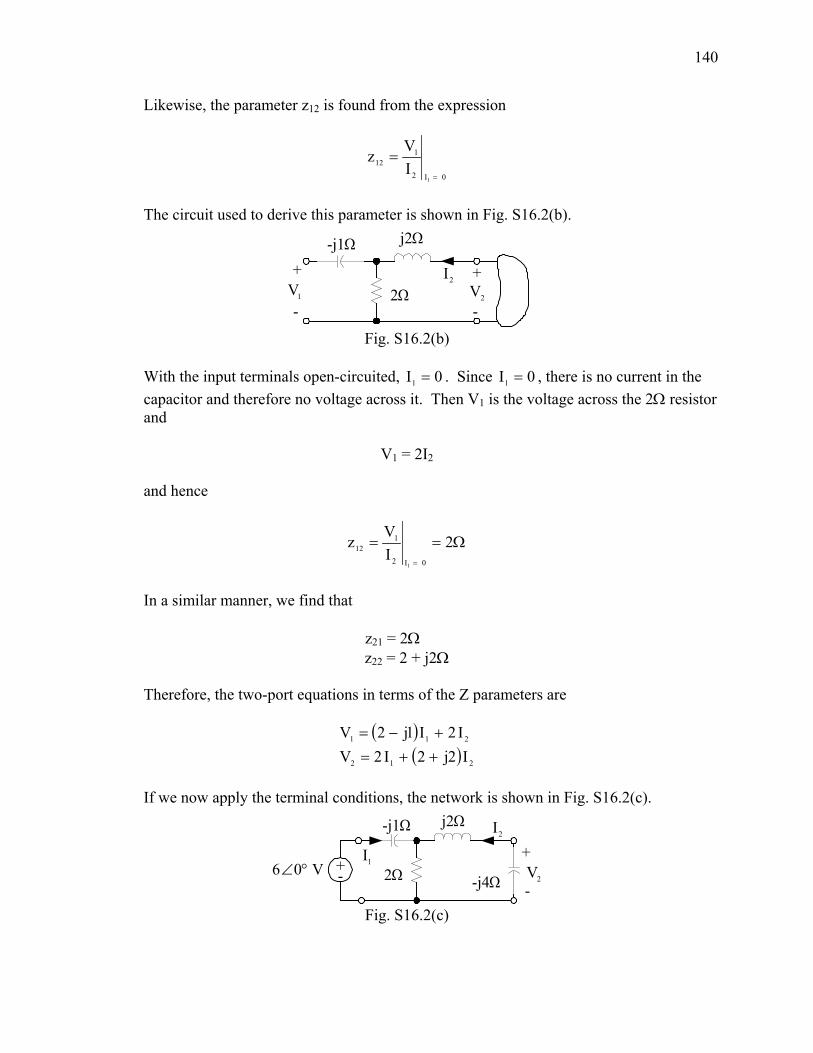
140
Likewise, the parameter z12 is found from the expression
0I2
112
1IV
z=
=
The circuit used to derive this parameter is shown in Fig. S16.2(b).
2Ω
j2Ω
1V+
-
2I
-j1Ω
2V+
-
Fig. S16.2(b) With the input terminals open-circuited, 0I1 = . Since 0I1 = , there is no current in the
capacitor and therefore no voltage across it. Then V1 is the voltage across the 2Ω resistor and
V1 = 2I2
and hence
Ω===
2IV
z0I2
112
1
In a similar manner, we find that z21 = 2Ω
z22 = 2 + j2Ω Therefore, the two-port equations in terms of the Z parameters are
( )( ) 212
211
I2j2I2VI2I1j2V
++=+−=
If we now apply the terminal conditions, the network is shown in Fig. S16.2(c).
2Ω
j2Ω
1I+-
2I-j1Ω
2V+
--j4ΩV06 °∠
Fig. S16.2(c)
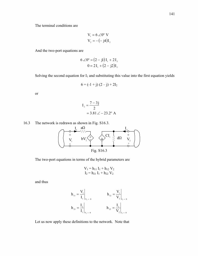
141
The terminal conditions are
( ) 22
1
I4jVV06V
−−=°∠=
And the two-port equations are
( )( ) 21
21
I2j2I20I2I1j206
−+=+−=°∠
Solving the second equation for I1 and substituting this value into the first equation yields
6 = (-1 + j) (2 – j) + 2I2 or
A2.2381.32
j37I2
°−∠=
−=
16.3 The network is redrawn as shown in Fig. S16.3.
2V+
-2bV +-
1V+
-
1CI2I1I aΩ
dΩ
Fig. S16.3
The two-port equations in terms of the hybrid parameters are
V1 = h11 I1 + h12 V2 I2 = h21 I1 + h22 V2
and thus
0I2
222
0V1
221
0I2
112
0V1
111
12
12
VI
hII
h
VVh
IVh
==
==
==
==
Let us now apply these definitions to the network. Note that
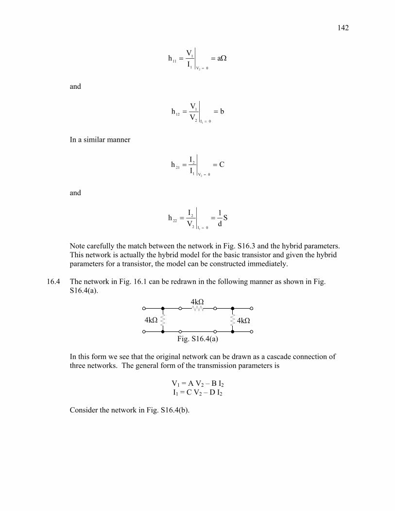
142
Ω===
aIV
h0V1
111
2
and
bVV
h0I2
112
1
===
In a similar manner
CII
h0V1
221
2
===
and
Sd1
VI
h0I2
222
1
===
Note carefully the match between the network in Fig. S16.3 and the hybrid parameters.
This network is actually the hybrid model for the basic transistor and given the hybrid parameters for a transistor, the model can be constructed immediately.
16.4 The network in Fig. 16.1 can be redrawn in the following manner as shown in Fig.
S16.4(a).
4kΩ
4kΩ
4kΩ
Fig. S16.4(a) In this form we see that the original network can be drawn as a cascade connection of
three networks. The general form of the transmission parameters is
V1 = A V2 – B I2 I1 = C V2 – D I2
Consider the network in Fig. S16.4(b).
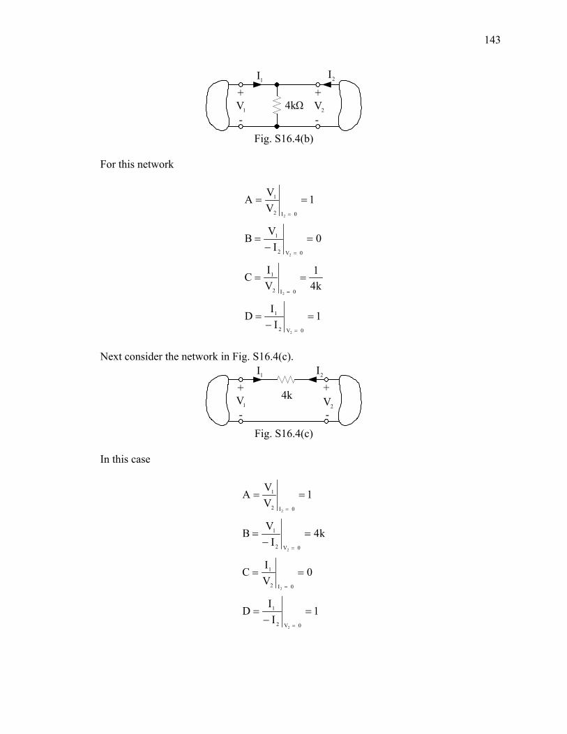
143
4kΩ1V+
-
2I
2V+
-
1I
Fig. S16.4(b)
For this network
1I
ID
k41
VIC
0I
VB
1VVA
0V2
1
0I2
1
0V2
1
0I2
1
2
2
2
2
=−
=
==
=−
=
==
=
=
=
=
Next consider the network in Fig. S16.4(c).
4k1V
+
-
2I
2V+
-
1I
Fig. S16.4(c)
In this case
1I
ID
0VIC
k4I
VB
1VVA
0V2
1
0I2
1
0V2
1
0I2
1
2
2
2
2
=−
=
==
=−
=
==
=
=
=
=
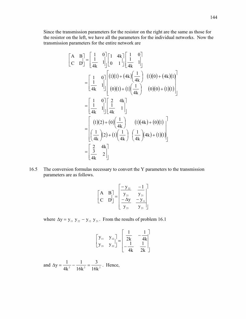
144
Since the transmission parameters for the resistor on the right are the same as those for the resistor on the left, we have all the parameters for the individual networks. Now the transmission parameters for the entire network are
( )( ) ( ) ( )( ) ( )( )
( )( ) ( ) ( )( ) ( )( )
( )( ) ( ) ( )( ) ( )( )
( ) ( ) ( ) ( )( )
⎥⎥⎦
⎤
⎢⎢⎣
⎡=
⎥⎥⎥⎥
⎦
⎤
⎢⎢⎢⎢
⎣
⎡
+⎟⎠⎞
⎜⎝⎛
⎟⎠⎞
⎜⎝⎛+⎟
⎠⎞
⎜⎝⎛
+⎟⎠⎞
⎜⎝⎛+
=
⎥⎥⎦
⎤
⎢⎢⎣
⎡
⎥⎥⎦
⎤
⎢⎢⎣
⎡=
⎥⎥⎥⎥
⎦
⎤
⎢⎢⎢⎢
⎣
⎡
+⎟⎠⎞
⎜⎝⎛+
+⎟⎠⎞
⎜⎝⎛+
⎥⎥⎦
⎤
⎢⎢⎣
⎡=
⎥⎥⎦
⎤
⎢⎢⎣
⎡⎥⎦
⎤⎢⎣
⎡
⎥⎥⎦
⎤
⎢⎢⎣
⎡=⎥
⎦
⎤⎢⎣
⎡
2k43
k42
11k4k4
1k4
112k4
1
10k41k4
1021
1k4
1k42
1k4
101
1100k4
1110
1k401k4
1k411
1k4
101
1k4
101
10k41
1k4
101
DCBA
16.5 The conversion formulas necessary to convert the Y parameters to the transmission
parameters are as follows.
⎥⎥⎥⎥
⎦
⎤
⎢⎢⎢⎢
⎣
⎡
−∆−
−−
=⎥⎦
⎤⎢⎣
⎡
21
11
21
2121
22
yy
yy
y1
yy
DCBA
where 21122211 yyyyy −=∆ . From the results of problem 16.1
⎥⎥⎥
⎦
⎤
⎢⎢⎢
⎣
⎡
−
−=⎥
⎦
⎤⎢⎣
⎡
k21
k41
k41
k21
yyyy
2221
1211
and 222 k16
3k161
k41y =−=∆ . Hence,
145
2
k41k21
yyD
k43
k41k163
yyC
k4
k411
y1B
2
k41k21
yy
A
21
11
2
21
21
21
22
=−
−
=−
=
=−
−
=∆−
=
=−−
=−
=
=−
−=
−=
These results check with those obtained in problem 16.4.
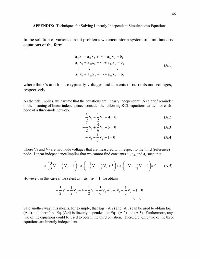
146
APPENDIX: Techniques for Solving Linearly Independent Simultaneous Equations In the solution of various circuit problems we encounter a system of simultaneous equations of the form
nnnn22n11n
2nn2222121
1nn1212111
bxaxaxa
bxaxaxabxaxaxa
=+++
=+++=+++
(A.1)
where the x’s and b’s are typically voltages and currents or currents and voltages, respectively. As the title implies, we assume that the equations are linearly independent. As a brief reminder of the meaning of linear independence, consider the following KCL equations written for each node of a three-node network:
04V21V
23
21 =−− (A.2)
05V65V
21
21 =++− (A.3)
01V31V 21 =−−− (A.4)
where V1 and V2 are two node voltages that are measured with respect to the third (reference) node. Linear independence implies that we cannot find constants a1, a2, and a3 such that
01V31Va5V
65V
21a4V
21V
23a 213212211 =⎟
⎠⎞
⎜⎝⎛ −−−+⎟
⎠⎞
⎜⎝⎛ ++−+⎟
⎠⎞
⎜⎝⎛ −− (A.5)
However, in this case if we select a1 = a2 = a3 = 1, we obtain
00
01V31V5V
65V
214V
21V
23
212121
=
=−−−++−−−+
Said another way, this means, for example, that Eqs. (A.2) and (A.3) can be used to obtain Eq. (A.4), and therefore, Eq. (A.4) is linearly dependent on Eqs. (A.2) and (A.3). Furthermore, any two of the equations could be used to obtain the third equation. Therefore, only two of the three equations are linearly independent.
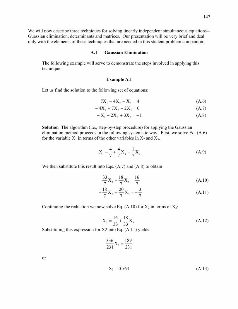
147
We will now describe three techniques for solving linearly independent simultaneous equations--Guassian elimination, determinants and matrices. Our presentation will be very brief and deal only with the elements of these techniques that are needed in this student problem companion.
A.1 Gaussian Elimination The following example will serve to demonstrate the steps involved in applying this
technique.
Example A.1 Let us find the solution to the following set of equations: 4XX4X7 321 =−− (A.6) 0X2X7X4 321 =−+− (A.7) 1X3X2X 321 −=+−− (A.8) Solution The algorithm (i.e., step-by-step procedure) for applying the Gaussian
elimination method proceeds in the following systematic way. First, we solve Eq. (A.6) for the variable X1 in terms of the other variables in X2 and X3.
321 X71X
74
74X ++= (A.9)
We then substitute this result into Eqs. (A.7) and (A.8) to obtain
7
16X7
18X733
32 =− (A.10)
73X
720X
718
32 −=+− (A.11)
Continuing the reduction we now solve Eq. (A.10) for X2 in terms of X3:
32 X3318
3316X += (A.12)
Substituting this expression for X2 into Eq. (A.11) yields
231189X
231336
3 =
or X3 = 0.563 (A.13)
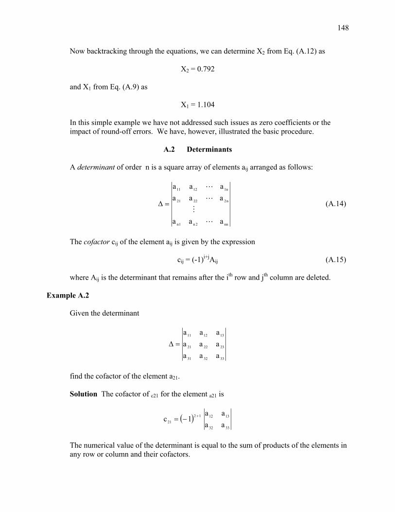
148
Now backtracking through the equations, we can determine X2 from Eq. (A.12) as
X2 = 0.792 and X1 from Eq. (A.9) as
X1 = 1.104 In this simple example we have not addressed such issues as zero coefficients or the
impact of round-off errors. We have, however, illustrated the basic procedure.
A.2 Determinants A determinant of order n is a square array of elements aij arranged as follows:
nn2n1n
n22221
n11211
aaa
aaaaaa
=∆ (A.14)
The cofactor cij of the element aij is given by the expression cij = (-1)i+jAij (A.15) where Aij is the determinant that remains after the ith row and jth column are deleted. Example A.2 Given the determinant
333231
232221
131211
aaaaaaaaa
=∆
find the cofactor of the element a21. Solution The cofactor of c21 for the element a21 is
( )3332
13121221 aa
aa1c +−=
The numerical value of the determinant is equal to the sum of products of the elements in
any row or column and their cofactors.

149
Example A.3 Let us determine the value of the determinant in Example A.2 using the first row. Solution
( ) ( ) ( )
3231
222113
3331
232112
3332
232211
1331
131221
121111
11
131312121111
aaaa
aaaaa
aaaaa
a
A1aA1aA1a
cacaca
+−=
−+−+−=
++=∆+++
Although the 2-by-2 determinants can be evaluated in the same manner, as illustrated
above, the result is simply
cbaddcba
−= (A.16)
Therefore, ∆ is
( ) ( ) ( )223132211323313321122332332211 aaaaaaaaaaaaaaa −+−−−=∆ We could evaluate the determinant using any row or column. The method of solving the set of simultaneous equations of the form shown in Eq. (A.1)
using determinants is known as Cramer’s rule. Cramer’s rule states that if ∆ ≠ 0 (that is, the equations are linearly independent), the value of the variable x1 in Eq. (A.1) is given by the expression
∆=
∆∆
= nnn2n
n2222
n1121
11
aab
aabaab
x
(A.17)
Where ∆1 is the determinant ∆ in which the first column is replaced with the column of
coefficients. In the general case, xi is given by an expression similar to Eq. (A.17) with the ith column replaced by the column of coefficients.
Example A.4
Let us solve the following equations using determinants.
150
2I1 – 4I2 = 8 -4I1 + 6I2 = -4
Solution In this case, ∆ defined by Eq. (A.16) is
( ) ( ) ( ) ( ) 444626442
−=−−−=−
−=∆
Then using Eq. (A.17)
( ) ( ) ( ) ( ) 84
44684
6448
I1 −=−
−−−=
−−
−
=
and
( ) ( ) ( ) ( ) 64
84424
4482
I2 −=−
−−−=
−−−
=
A.3 Matrices
A matrix is defined to be a rectangular array of numbers arranged in rows and columns
and written in the form
⎥⎥⎥⎥
⎦
⎤
⎢⎢⎢⎢
⎣
⎡
mn2m1m
n22221
n11211
aaa
aaaaaa
This array is called an m by n (m × n) matrix because is has m rows and n columns. A
matrix is a convenient way of representing arrays of numbers; however, one must remember that the matrix itself has no numerical value. In the preceding array the numbers or functions aij are called the elements of the matrix. Any matrix that has the same number of rows as columns is called a square matrix.
Example A.5
Are the following matrices?
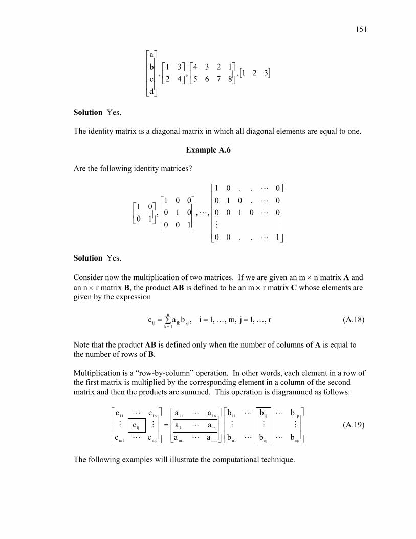
151
[ ]321,87651234
,4231
,
dcba
⎥⎦
⎤⎢⎣
⎡⎥⎦
⎤⎢⎣
⎡
⎥⎥⎥⎥
⎦
⎤
⎢⎢⎢⎢
⎣
⎡
Solution Yes. The identity matrix is a diagonal matrix in which all diagonal elements are equal to one.
Example A.6 Are the following identity matrices?
⎥⎥⎥⎥⎥⎥
⎦
⎤
⎢⎢⎢⎢⎢⎢
⎣
⎡
⎥⎥⎥
⎦
⎤
⎢⎢⎢
⎣
⎡
⎥⎦
⎤⎢⎣
⎡
1..00
001000.0100..01
,,100010001
,1001
Solution Yes. Consider now the multiplication of two matrices. If we are given an m × n matrix A and
an n × r matrix B, the product AB is defined to be an m × r matrix C whose elements are given by the expression
r,,1j,m,,1i,bacn
1kkjikij …… ==∑=
= (A.18)
Note that the product AB is defined only when the number of columns of A is equal to
the number of rows of B. Multiplication is a “row-by-column” operation. In other words, each element in a row of
the first matrix is multiplied by the corresponding element in a column of the second matrix and then the products are summed. This operation is diagrammed as follows:
⎥⎥⎥
⎦
⎤
⎢⎢⎢
⎣
⎡
⎥⎥⎥
⎦
⎤
⎢⎢⎢
⎣
⎡=
⎥⎥⎥
⎦
⎤
⎢⎢⎢
⎣
⎡
npnj1n
p1ij11
mn1m
in1i
n111
mp1m
ij
p111
bbb
bbb
aaaaaa
ccc
cc (A.19)
The following examples will illustrate the computational technique.
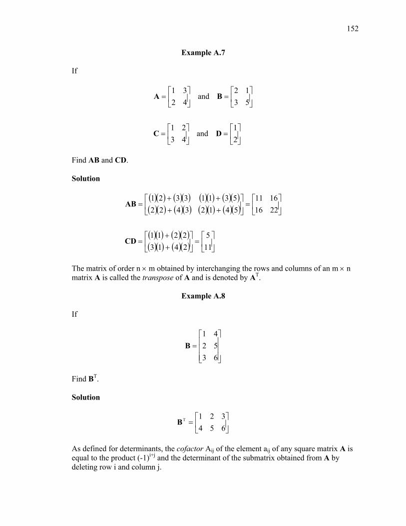
152
Example A.7 If
⎥⎦
⎤⎢⎣
⎡=⎥
⎦
⎤⎢⎣
⎡=
⎥⎦
⎤⎢⎣
⎡=⎥
⎦
⎤⎢⎣
⎡=
21
and4321
5312
and4231
DC
BA
Find AB and CD. Solution
( )( ) ( )( ) ( )( ) ( )( )( )( ) ( )( ) ( )( ) ( )( )
( )( ) ( )( )( )( ) ( )( ) ⎥
⎦
⎤⎢⎣
⎡=⎥
⎦
⎤⎢⎣
⎡++
=
⎥⎦
⎤⎢⎣
⎡=⎥
⎦
⎤⎢⎣
⎡++++
=
115
24132211
22161611
5412342253113321
CD
AB
The matrix of order n × m obtained by interchanging the rows and columns of an m × n
matrix A is called the transpose of A and is denoted by AT.
Example A.8 If
⎥⎥⎥
⎦
⎤
⎢⎢⎢
⎣
⎡=
635241
B
Find BT. Solution
⎥⎦
⎤⎢⎣
⎡=
654321TB
As defined for determinants, the cofactor Aij of the element aij of any square matrix A is
equal to the product (-1)i+j and the determinant of the submatrix obtained from A by deleting row i and column j.
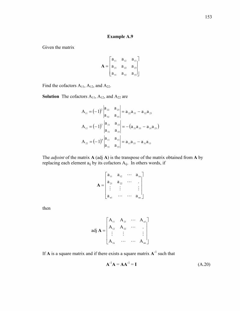
153
Example A.9
Given the matrix
⎥⎥⎥
⎦
⎤
⎢⎢⎢
⎣
⎡=
333231
232221
131211
aaaaaaaaa
A
Find the cofactors A11, A12, and A22. Solution The cofactors A11, A12, and A22 are
( )
( ) ( )
( ) 133133113331
1311422
233133213331
2321312
233233223332
2322211
aaaaaaaa
1A
aaaaaaaa
1A
aaaaaaaa
1A
−=−=
−−=−=
−=−=
The adjoint of the matrix A (adj A) is the transpose of the matrix obtained from A by
replacing each element aij by its cofactors Aij. In others words, if
⎥⎥⎥⎥
⎦
⎤
⎢⎢⎢⎢
⎣
⎡
=
nn1n
2221
n11211
aa
.aaaaa
A
then
⎥⎥⎥⎥
⎦
⎤
⎢⎢⎢⎢
⎣
⎡
=
nnn1
2212
1n2111
AA
.AAAAA
adj A
If A is a square matrix and if there exists a square matrix A-1 such that A-1A = AA-1 = I (A.20)
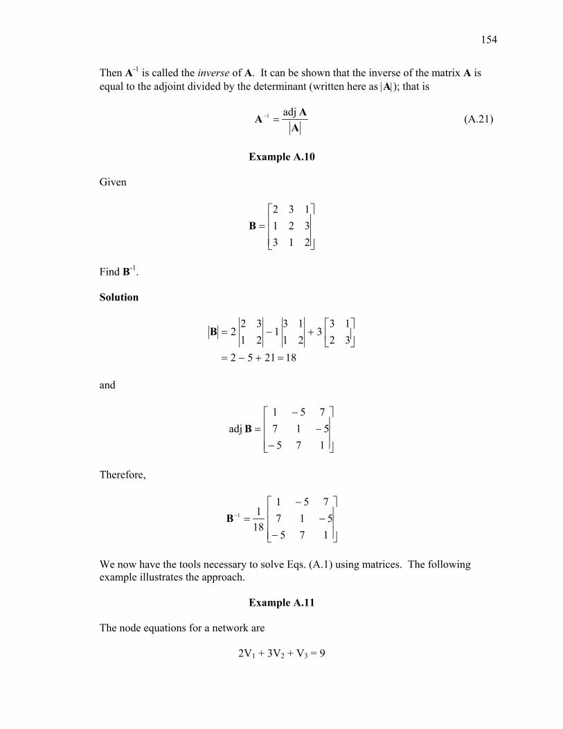
154
Then A-1 is called the inverse of A. It can be shown that the inverse of the matrix A is equal to the adjoint divided by the determinant (written here as |A|); that is
A
AA adj1 =− (A.21)
Example A.10
Given
⎥⎥⎥
⎦
⎤
⎢⎢⎢
⎣
⎡=
213321132
B
Find B-1. Solution
1821523213
32113
12132
2
=+−=
⎥⎦
⎤⎢⎣
⎡+−=B
and
⎥⎥⎥
⎦
⎤
⎢⎢⎢
⎣
⎡
−−
−=
175517
751adj B
Therefore,
⎥⎥⎥
⎦
⎤
⎢⎢⎢
⎣
⎡
−−
−=−
175517
751
1811B
We now have the tools necessary to solve Eqs. (A.1) using matrices. The following
example illustrates the approach.
Example A.11 The node equations for a network are
2V1 + 3V2 + V3 = 9
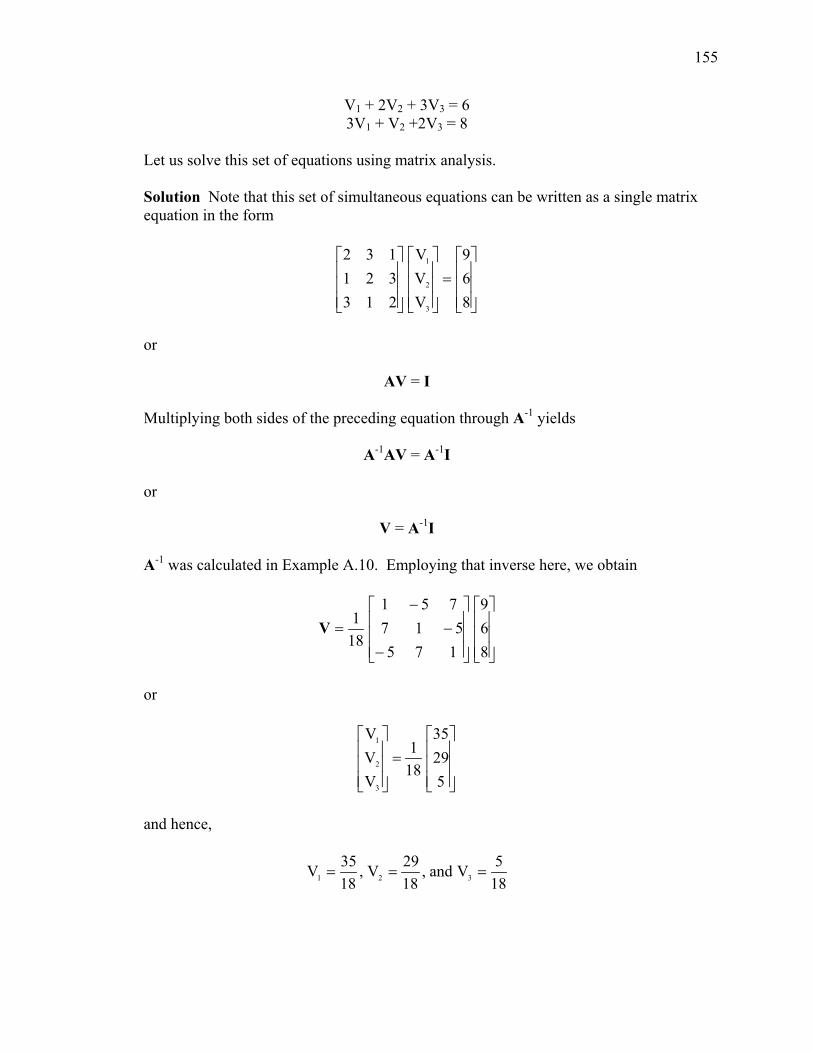
155
V1 + 2V2 + 3V3 = 6 3V1 + V2 +2V3 = 8
Let us solve this set of equations using matrix analysis. Solution Note that this set of simultaneous equations can be written as a single matrix
equation in the form
⎥⎥⎥
⎦
⎤
⎢⎢⎢
⎣
⎡=
⎥⎥⎥
⎦
⎤
⎢⎢⎢
⎣
⎡
⎥⎥⎥
⎦
⎤
⎢⎢⎢
⎣
⎡
869
VVV
213321132
3
2
1
or
AV = I Multiplying both sides of the preceding equation through A-1 yields
A-1AV = A-1I or
V = A-1I A-1 was calculated in Example A.10. Employing that inverse here, we obtain
⎥⎥⎥
⎦
⎤
⎢⎢⎢
⎣
⎡
⎥⎥⎥
⎦
⎤
⎢⎢⎢
⎣
⎡
−−
−=
869
175517
751
181V
or
⎥⎥⎥
⎦
⎤
⎢⎢⎢
⎣
⎡=
⎥⎥⎥
⎦
⎤
⎢⎢⎢
⎣
⎡
52935
181
VVV
3
2
1
and hence,
185Vand,
1829V,
1835V 321 ===
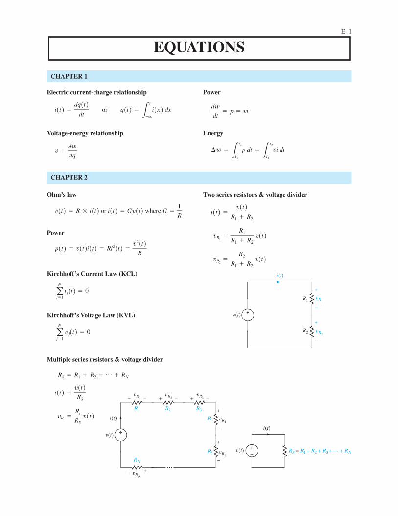
E–1
EQUATIONS
CHAPTER 1
Electric current-charge relationship
Voltage-energy relationship
Power
Energy
¢w = 3t2
t1
p dt = 3t2
t1
vi dt
dw
dt= p = vi
v =dw
dq
i(t) =dq(t)
dt or q(t) = 3
t
-qi(x) dx
CHAPTER 2
Ohm’s law
v(t)=R*i(t) or i(t)=Gv(t) where
Power
p(t)=v(t)i(t)
Kirchhoff’s Current Law (KCL)
Kirchhoff’s Voltage Law (KVL)
Two series resistors & voltage divider
vR1
vR2
R1
R2
v(t)
i(t)
+
–
+
–
vR2=
R2
R1 + R2v(t)
vR1=
R1
R1 + R2v(t)
i(t) =v(t)
R1 + R2
aN
j= 1vj(t) = 0
aN
j= 1ij(t) = 0
= Ri2(t) =v2(t)
R
G =1
R
Multiple series resistors & voltage divider
vRi=
Ri
RSv(t)
i(t) =v(t)
RS
RS = R1 + R2 + p + RN
RN
RS = R1 + R2 + R3 + … + RN
R1 R2 R3
R4
R5
vR1vR2
vR3
vRN
vR4
vR5
v(t)
v(t)
i(t)
i(t)
+
+
–
+
–
+ – + – + –
–
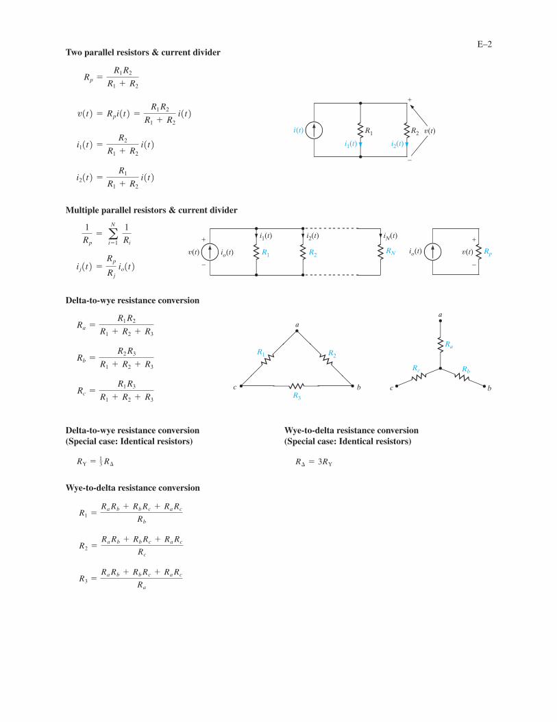
Two parallel resistors & current divider
Multiple parallel resistors & current divider
Delta-to-wye resistance conversion
Rc =R1 R3
R1 + R2 + R3
Rb =R2 R3
R1 + R2 + R3
Ra =R1 R2
R1 + R2 + R3
ij(t) =Rp
Rjio(t)
1
Rp= a
N
i= 1
1
Ri
i2(t) =R1
R1 + R2i(t)
i1(t) =R2
R1 + R2i(t)
v(t) = Rp i(t) =R1 R2
R1 + R2i(t)
Rp =R1 R2
R1 + R2
E–2
R1 R2 v(t)i(t)
i1(t) i2(t)
+
–
RpRNR1 R2 v(t)v(t) io(t)
i1(t) i2(t) iN(t)
io(t)
+ +
––
R1
a
bcR3
R2
a
bc
RbRc
Ra
Delta-to-wye resistance conversion(Special case: Identical resistors)
Wye-to-delta resistance conversion
Wye-to-delta resistance conversion(Special case: Identical resistors)
R¢ = 3RY
R3 =Ra Rb + Rb Rc + Ra Rc
Ra
R2 =Ra Rb + Rb Rc + Ra Rc
Rc
R1 =Ra Rb + Rb Rc + Ra Rc
Rb
RY = 13 R¢

CHAPTER 3
E–3
Ohm’s law expressed in node voltages
Ohm’s law expressed in loop currents
Ideal op amp
v+
v–
i+
i–∞
v+ = v-
i+ = i- = 0
vS2
vS1
v1
v3 v4
v2 v5
R1
R2
R3 R4
R5
i1 i2+
–
+
+
+ +– –
–
–
A B C
F E D
v3 = Ai1 - i2B R3
vm
+
–
vN
+
–
Node m Node N
i
R
+(vm–vN)-
i =vm - vN
R
Equivalent circuit forms
R1
R2
R1 + R2
V1
V2
V1 – V2
R1R2
R1 + R2
R1 R2————
CHAPTER 4
CHAPTER 5
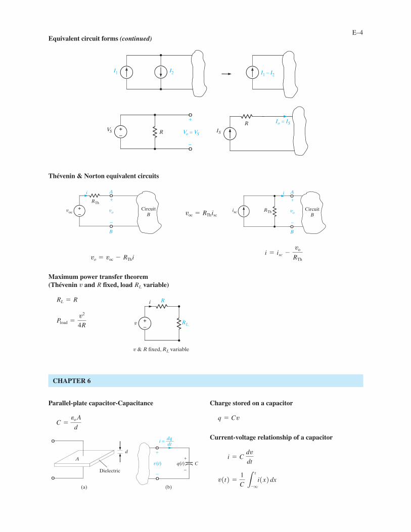
Equivalent circuit forms (continued)
I1 I2 I1 – I2
VS Vo = VS
Io = IS
IS
R
R
+
–
E–4
Thévenin & Norton equivalent circuits
Maximum power transfer theorem(Thévenin and fixed, load variable)
Pload =v2
4R
RL = R
RLRv
i = isc -vo
RThvo = voc - RTh i
i
iscCircuit
B
A
B
vo
+
–
RThvoc = RTh isc
i
voc
A
B
CircuitB
vo
+
–
RTh
Parallel-plate capacitor-Capacitance Charge stored on a capacitor
Current-voltage relationship of a capacitor
v(t) =1
C 3t
-qi(x) dx
i = Cdv
dt
q = Cv
dqdt
(a)
Dielectric
AC
d
(b)
q(t)v(t)
+
–
i = ——
+
–
C =eo Ad
RL
Ri
v
v & R fixed, RL variable
CHAPTER 6
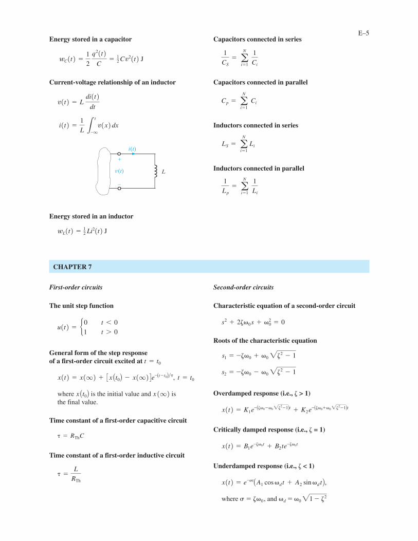
Energy stored in a capacitor
Current-voltage relationship of an inductor
Energy stored in an inductor
Capacitors connected in series
Capacitors connected in parallel
Inductors connected in series
Inductors connected in parallel
1
Lp= a
N
i= 1
1
Li
LS = aN
i= 1Li
Cp = aN
i= 1Ci
1
CS= a
N
i= 1
1
Ci
wL(t) = 12 Li2(t) J
Lv(t)
i(t)
+
–
i(t) =1
L 3t
-qv(x) dx
v(t) = Ldi(t)
dt
wC(t) =1
2
q2(t)
C= 1
2 Cv2(t) J
E–5
First-order circuits
The unit step function
General form of the step responseof a first-order circuit excited at
where is the initial value and isthe final value.
Time constant of a first-order capacitive circuit
Time constant of a first-order inductive circuit
Second-order circuits
Characteristic equation of a second-order circuit
Roots of the characteristic equation
Overdamped response (i.e., > 1)
Critically damped response (i.e., = 1)
Underdamped response (i.e., < 1)
where and d = 021 - 2 = 0 ,
x(t) = e-tAA1 cos d t + A2 sin d tB,
x(t) = B1 e-0 t + B2 te-0 t
x(t) = K1 e-A0-022- 1Bt + K2 e-A0+022- 1Bt
s2 = -0 - 022 - 1
s1 = -0 + 022 - 1
s2 + 20 s + 20 = 0
=L
RTh
= RTh C
x (q)x At0Bx(t) = x(q) + Cx At0B - x(q) De-At- t0B, t = t0
t = t0
u(t) = b0
1
t 6 0
t 7 0
CHAPTER 7
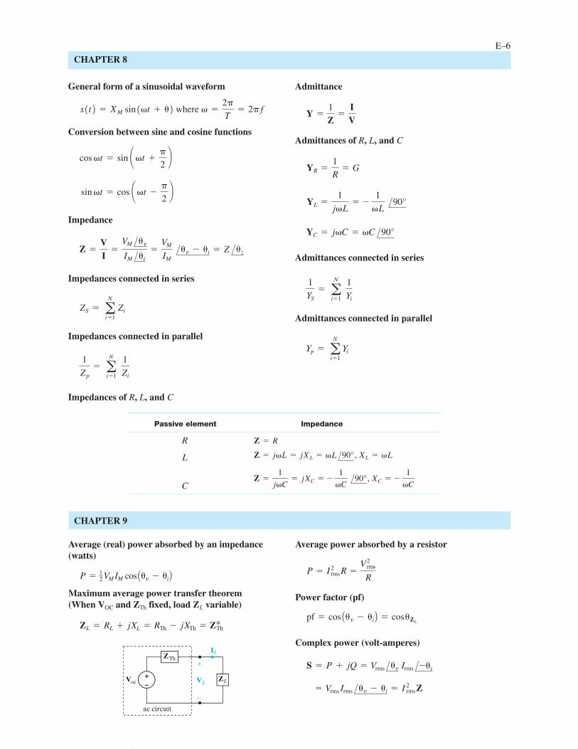
E–6
General form of a sinusoidal waveform
where
Conversion between sine and cosine functions
Impedance
Impedances connected in series
Impedances connected in parallel
Admittance
Admittances of R, L, and C
Admittances connected in series
Admittances connected in parallel
Yp = aN
i= 1Yi
1
YS= a
N
i= 1
1
Yi
YC = jC = C/90°
YL =1
jL= -
1
L/90°
YR =1
R= G
Y =1
Z=
IV
1
Zp= a
N
i= 1
1
Zi
ZS = aN
i= 1Zi
Z =VI=
VM/v
IM/i=
VM
IM/v - i = Z/z
sin t = cos at -
2b
cos t = sin at +
2b
=2
T= 2fx(t) = XM sin (t + )
Impedances of R, L, and C
Passive element Impedance
R
L
CZ =
1
jC= jXC = -
1
C/90° , XC = -
1
C
Z = jL = jXL = L/90° , XL = L
Z = R
CHAPTER 9
Average (real) power absorbed by an impedance(watts)
Maximum average power transfer theorem(When and fixed, load variable)
Average power absorbed by a resistor
Power factor (pf)
Complex power (volt-amperes)
= Vrms Irms/v - i = I2rms Z
S = P + jQ = Vrms/v Irms/-i
pf = cos Av - iB = cos ZL
P = I2rms R =
V2rms
R
oc
+
–
VL
ac circuit
Voc
ZTh
ZL
IL
ZL = RL + jXL = RTh - jXTh = Z*Th
ZLZThVOC
P = 12 VM IM cos Av - iB
CHAPTER 8
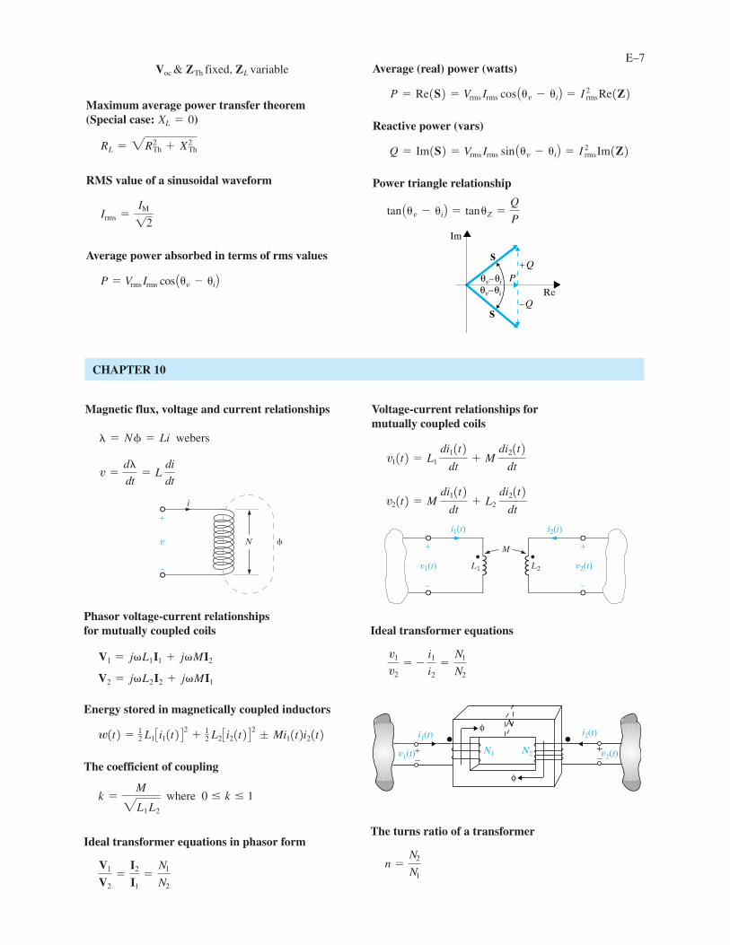
E–7
Maximum average power transfer theorem(Special case: )
RMS value of a sinusoidal waveform
Average power absorbed in terms of rms values
Average (real) power (watts)
Reactive power (vars)
Power triangle relationship
tan Av - iB = tan Z =Q
P
Q = Im(S) = Vrms Irms sin Av - iB = I2rms Im(Z)
P = Re(S) = Vrms Irms cos Av - iB = I2rms Re(Z)
P = Vrms Irms cos Av - iB
Irms =IM
12
RL = 2R2Th + X2
Th
XL = 0
Voc & ZTh fixed, ZL variable
Im
Reθv–θi
θv–θi
+Q
–Q
P
S
S
CHAPTER 10
Magnetic flux, voltage and current relationships
=N=Li webers
Voltage-current relationships formutually coupled coils
L1 L2
M
v1(t) v2(t)
i1(t) i2(t)
+
–
+
–
v2(t) = Mdi1(t)
dt+ L2
di2(t)
dt
v1(t) = L1
di1(t)
dt+ M
di2(t)
dt
v N
+
–
i
v =d
dt= L
di
dt
Phasor voltage-current relationshipsfor mutually coupled coils
Energy stored in magnetically coupled inductors
The coefficient of coupling
Ideal transformer equations in phasor form
Ideal transformer equations
The turns ratio of a transformer
n =N2
N1
i1(t) i2(t)
v1(t) v2(t)+–
φ
φ
N1 N2+–
• •A
v1
v2= -
i1
i2=
N1
N2
V1
V2=
I2
I1=
N1
N2
k =M
2L1 L2
where 0 k 1
w(t) = 12 L1 C i1(t) D2 + 1
2 L2 C i2(t) D2 ; Mi1(t)i2(t)
V2 = jL2 I2 + jMI1
V1 = jL1 I1 + jMI2
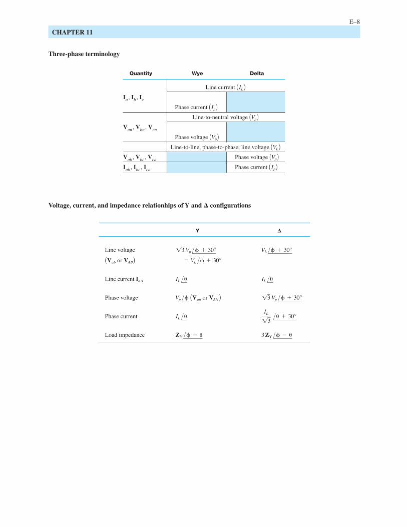
Three-phase terminology
Voltage, current, and impedance relationhips of Y and configurations
E–8
Quantity Wye Delta
Line current
Ia , Ib , Ic
Phase current
Line-to-neutral voltage
Van , Vbn , Vcn
Phase voltage
Line-to-line, phase-to-phase, line voltage
Vab , Vbc , Vca Phase voltage
Iab , Ibc , Ica Phase current AIpBAVpBAVLB
AVpB
AVpBAIpB
AILB
Y
Line voltage
Line current
Phase voltage
Phase current
Load impedance 3 ZY / - ZY / -
IL
13/ + 30°IL /
13 Vp / + 30°Vp / AVan or VANB
IL /IL /IaA
= VL / + 30°AVab or VABBVL / + 30°13 Vp / + 30°
CHAPTER 11
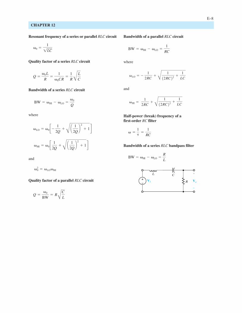
Resonant frequency of a series or parallel RLC circuit
Quality factor of a series RLC circuit
Bandwidth of a series RLC circuit
where
and
Quality factor of a parallel RLC circuit
Bandwidth of a parallel RLC circuit
where
and
Half-power (break) frequency of afirst-order RC filter
Bandwidth of a series RLC bandpass filter
L
V1 Vo
+
–
C
R
BW = HI - LO =R
L
=1
=1
RC
HI =1
2RC+ B
1
(2RC)2 +1
LC
LO = -1
2RC+ B
1
(2RC)2 +1
LC
BW = HI - LO =1
RC
Q =0
BW= RA
C
L
20 = LO HI
HI = 0 c 1
2Q+ B a
1
2Qb 2
+ 1 d
LO = 0 c- 1
2Q+ B a
1
2Qb 2
+ 1 d
BW = HI - LO =0
Q
Q =0 L
R=
1
0 CR=
1
RBL
C
0 =1
1LC
E–8
CHAPTER 12
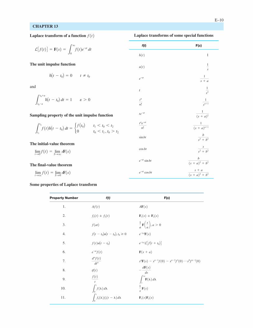
E–10
Property Number f(t) F(s)
1.
2.
3.
4.
5.
6.
7.
8.
9.
10.
11. F1(s)F2(s)3t
0f1()f2(t - ) d
1
sF(s)3
t
0f() d
3q
sF() d
f(t)
t
-dF(s)
dstf(t)
snF(s) - sn- 1f(0) - sn-2f1(0) p s0fn- 1(0)dnf(t)
dtn
F(s + a)e-atf(t)
e-t0 sL CfAt + t0B Df(t)uAt - t0Be-t0 sF(s)fAt - t0BuAt - t0B, t0 0
1
aF a s
ab , a 7 0f(at)
F1(s) ; F2(s)f1(t) ; f2(t)
AF(s)Af(t)
Laplace transform of a function
The unit impulse function
and
Sampling property of the unit impulse function
The initial-value theorem
The final-value theorem
Laplace transforms of some special functions
f(t) F(s)
1
t
s + a
(s + a)2 + b2e-at cos bt
b
(s + a)2 + b2e-at sin bt
s
s2 + b2cos bt
b
s2 + b2sin bt
1
(s + a)n+ 1
tne-at
n!
1
(s + a)2te-at
1
sn+ 1
tn
n!
1
s2
1
s + ae-at
1
su(t)
(t)
limtSq
f(t) = limSS0
sF(s)
limtS0
f(t) = limSSq
sF(s)
3t2
t1
f(t)At - t0B dt = bf At0B0
t1 6 t0 6 t2
t0 6 t1 , t0 7 t2
3t0+
t0-
At - t0B dt = 1 7 0
At - t0B = 0 t Z t0
L Cf(t) D = F(s) = 3q
0f(t)e-st dt
f(t)
Some properties of Laplace transform
CHAPTER 13
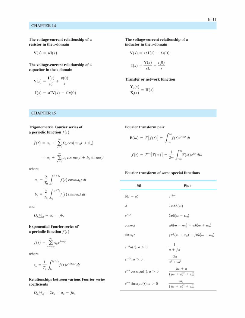
E–11
The voltage-current relationship of aresistor in the s-domain
The voltage-current relationship of acapacitor in the s-domain
The voltage-current relationship of ainductor in the s-domain
Transfer or network function
Yo(s)
Xi(s)= H(s)
I(s) =V(s)
sL+
i(0)
s
V(s) = sLI(s) - Li(0)
I(s) = sCV(s) - Cv(0)
V(s) =I(s)
sC+
v(0)
s
V(s) = RI(s)
CHAPTER 14
Trigonometric Fourier series ofa periodic function
where
and
Exponential Fourier series ofa periodic function
where
Relationships between various Fourier seriescoefficients
Fourier transform pair
Fourier transform of some special functions
f(t) = F-1 CF() D = 1
2 3q
-qF()ejt d
F() = F Cf(t) D = 3q
-qf(t)e-jt dt
Dn/n = 2cn = an - jbn
cn =1
T0 3t1+T0
t1
f(t)e-jn0 t dt
f(t) = aq
n=-qcn ejn0 t
f(t)
Dn/n = an - jbn
bn =2
T0 3t1+T0
t1
f(t) sin n0 t dt
an =2
T0 3t1+T0
t1
f(t) cos n0 t dt
= a0 + aq
n= 1an cos n0 t + bn sin n0 t
f(t) = a0 + aq
n= 1Dn cos An0 t + nBf(t)
f(t)
0
(j + a)2 + 20
e-at sin 0 tu(t), a 7 0
j + a
(j + a)2 + 20
e-at cos 0 tu(t), a 7 0
2a
a2 + 2e- ∑t∑, a 7 0
1
a + je-at u(t), a 7 0
jA + 0B - jA - 0Bsin 0 t
A - 0B + A + 0Bcos 0 t
2A - 0Bej0 t
2A()A
e-ja(t - a)
F()
CHAPTER 15
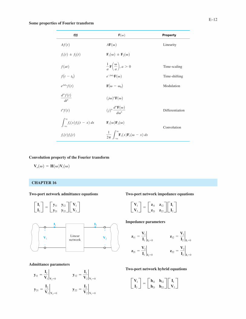
Some properties of Fourier transform
Convolution property of the Fourier transform
Vo() = H()Vi()
E–12
f(t) Property
Linearity
Time-scaling
Time-shifting
Modulation
Differentiation
Convolution1
2 3q
-qF1(x)F2( - x) dxf1(t)f2(t)
F1()F2()3q
-qf1(x)f2(t - x) dx
(j)ndn F()
dntnf(t)
(j)n F()dn f(t)
dtn
FA - 0Bejt0 f(t)
e-jt0 F()fAt - t0B
1a
F a
ab , a 7 0f(at)
F1() ; F2()f1(t) ; f2(t)
AF()Af(t)
F()
Two-port network admittance equations
Admittance parameters
Two-port network impedance equations
Impedance parameters
Two-port network hybrid equations
BV1
I2R = Bh11
h21
h12
h22R B I1
V2R
z22 =V2
I2
2I1=0
z21 =V2
I1
2I2=0
z12 =V1
I2
2I1=0
z11 =V1
I1
2I2=0
BV1
V2R = B z11
z21
z12
z22R B I1
I2R
y22 =I2
V2
2V1=0
y21 =I2
V1
2V2=0
y12 =I1
V2
2V1=0
y11 =I1
V1
2V2=0
V1 V2
I1 I2
Linearnetwork
B I1
I2R = By11
y21
y12
y22R BV1
V2R
CHAPTER 16
Hybrid parameters
Two-port network transmission equations
Transmission parameters
D =I1
-I2
2V2=0
C =I1
V2
2I2=0
B =V1
-I2
2V2=0
A =V1
V2
2I2=0
BV1
I1R = BA
CBDR B V2
-I2R
h22 =I2
V2
2I1=0
h21 =I2
I1
2V2=0
h12 =V1
V2
2I1=0
h11 =V1
I1
2V2=0
E–13
B h11
h21
h12
h22RD B
D
-1
D
¢T
DCD
TD 1
y11
y21
y11
-y12
y11
¢Y
y11
TD ¢Z
z22
-z21
z22
z12
z22
1
z22
T
D -¢H
h21
-h22
h21
-h11
h21
-1
h21
TcA BC D
dD -y22
y21
-¢Y
y21
-1
y21
-y11
y21
TD z11
z21
1
z21
¢Z
z21
z22
z21
T
D 1
h11
h21
h11
-h12
h11
¢H
h11
TD DB
-1
B
-¢T
BAB
TB y11
y21
y12
y22RD z22
¢Z
-z21
¢Z
-z12
¢Z
z11
¢Z
T
D ¢H
h22
-h21
h22
h12
h22
1
h22
TDAC1
C
¢T
CDC
TD y22
¢Y
-y21
¢Y
-y12
¢Y
y11
¢Y
TB z11
z21
z12
z22R
Two-port network parameter conversions