Embed Size (px)
Citation preview

Fifth International Symposium on Space Terahertz Technology Page 611
DESIGN AND REALIZATION OF GaAs D-BAND IMPATT
OSCILLATORS
M. Tschernitz and J. Freyer
Lehrstuhl fiir Allgemeine Elektrotechnik und Angewandte Elektronik
4rcisstr 21 80290 Miinchen, Germany
Abstract
GaAs IMPATT oscillators for c'w operation at D-band frequencies
are designed and fabricated. The active devices are encapsulated using
the novel module technique on diamond heat sinks. For the design
of the module a CAD-software package is applied which considers the
complete outer waveguide resonator structure as well as the module en-
capsulation structure. As active devices GaAs single-drift flat profile
IMP ATT diodes and Read-type IMPATT diodes are investigated. The
Read-type diode structure is designed by the help of a numerical pro-
gram for calculation of the device impedance. The main design feature
is low dc input voltage yielding high dc current density. Experimental
results for rf output power and noise behaviour are given for both types
of diodes in the frequency range from 110-150 Gllz.
1 Introduction
Avalanche transit-time devices are keyelernen.ts for power generation at mm-
wave frequencies and can be applied in various systems, for example as low-
noise local oscillator or self-oscillating mixer. For the realization of ram-wave
oscillators the most critical parameter that determines rf-performance is the

Page 612 Fifth International Symposium on Space Terahertz Technology
impedance matching of the active diode to the resonant circuit. In particular
at elevated mm-wave frequencies the rf-behaviour predominantly is determined
by the diode encapsulation structure. Up to now, the encapsulation structure
mainly is realized with the help of quartz stand-offs and gold bond ribbons.
Because of the intricated encapsulation process high failure rates occur and the
reproducibility of the rf-behaviour is a critical task. A decisive improvement
is achieved from MMIC-technique for the fabrication of mm-wave oscillators
which yields excellent reproducibility due to the applied photoresist technology
(see for example [11[21). In order to bring forward the advantage of photoresist
technology for encapsulation of two-terminal devices also on diamond heat-
sinks an encapsulation module representing a monolithic integration of active
diode and sourrounding standoff structure has been developed [3]. Good rf-
performance achieved by the help of this technique is demonstrated at W-band
frequencies, yielding a conversion efficiency of more than 10 % at 90 Gliz with
a GaAs IMPATT diode [4].
This work is concerned with the design and fabrication of modules and reso-
nator structures for 0-hand frequencies. Resonator and module are optimized
using a finite element CAD software package for calculation of the entire im-
pedance. As active devices conventional applied single-drift flat-profile GaAs
IMPATT-diodes as well as Read-type diodes are investigated. Experimental
values for rf-output power and noise measure for the frequency range from
110-150 GHz are reported.
2 The encapsulation module
The principal cross-section of the module can be seen in Fig. 1. Initial material
for the fabrication is semiinsulating GaAs on which a Ga.AlAs etch-stop layer

Fifth International Symposium on Space Terahertz Technology Page 613
followed by the desired layer sequence for the active diode is grown. For the
epitaxial growth standard molecular beam epitaxy is used. The semiin.sulating
GaAs material is used for electrical isolation of the diode from the stand-off
structure and replaces seperately mounted quartz stand-offs. The diode top
contact structure is realized by selective etching technology for GaAs substi-
tuting the gold bond ribbons (see Fig. 1). The REM photograph in Fig. 2
shows a module seen from the epitaxial layer side, i.e. the side which has to be
bonded onto the heat-sink. The stand-off structure guarantees the mechanical
fixing of the module on the diamond heat-sink. Photoresist technology app-
lied for the realization of all critical dimensions of the module results in high
reproducibility. Instead of thermocompression bonding of a tiny single diode
(diameter 15-20 ,um) on a diamond heat sink and contacting this device with
gold bond ribbons the whole module is bonded in one step on the diamond
heat sink.
3 The resonator structure
The modules are incorporated into a D-band waveguide resonator termina-
ted at one end with a sliding short for tuning. A disk-type radial resonator
structure is mounted directly on the module top-metallization. This leads to
a height of the resonant disk above the waveguide bottom which is equal to
the module height (module dimensions: see Fig. 1). This distance is much
lower as compared to conventionally encapsulated devices with quartz stand-
offs. Therefore, the resonant structure was investigated in order to ensure that
impedance matching between active device and resonator is possible. For the
computer simulation a finite element CAD sofware package is used ('HFSS',
Hewlett Packard). The program considers the complete outer resonator struc-
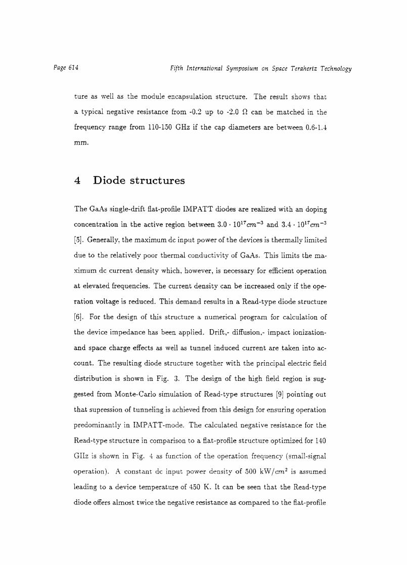
Page 614 Fifth International Symposium on Space Terahertz Technology
ture as well as the module encapsulation structure. The result shows that
a typical negative resistance from -0.2 up to -2.0 can be matched in the
frequency range from 110-130 GHz if the cap diameters are between 0.6-1.4
MM.
4 Diode structures
The GaAs single-drift flat-profile IMPATT diodes are realized with an doping
concentration in the active region between 3.0 • 10 17crn-3 and 3.4 • 1017cm-3
[51. Generally, the maximum dc input power of the devices is thermally limited
due to the relatively poor thermal conductivity of GaAs. This limits the ma-
ximum dc current density which, however, is necessary for efficient operation
at elevated frequencies. The current density can be increased only if the ope-
ration voltage is reduced. This demand results in a Read-type diode structure
[61. For the design of this structure a numerical program for calculation of
the device impedance has been applied. Drift,- diffusion,- impact ionization-
and space charge effects as well as tunnel induced current are taken into ac-
count. The resulting diode structure together with the principal electric field
distribution is shown in Fig. 3. The design of the high field region is sug-
gested from Monte-Carlo simulation of Read-type structures [9] pointing out
that supression of tunneling is achieved from this design for ensuring operation
predominantly in IMPATT-mode. The calculated negative resistance for the
Read-type structure in comparison to a fiat-profile structure optimized for 140
Gliz is shown in Fig. 4 as function of the operation frequency (small-signal
operation). A constant dc input power density of 500 kW/cm 2 is assumed
leading to a device temperature of 450 K. It can be seen that the Read-type
diode offers almost twice the negative resistance as compared to the fiat-profile
Fifth international Symposium on Space Terahertz Technology Page 615
structure.
For ensuring low-ohmic contacts a well established contact system for GaAs
has been applied for all diodes investigated: TiPdAu for the pt -ohmic contact
and AuGeNi/Au for the n + -ohmic contact.
5 Experimental results
The measured breakdown voltage for the flat-profile diodes is between 7.8-
8.2 V. The value of 6.2 V for the Read-type diode demonstrates the achieved
reduction of operation voltage. Thus, the maximum dc current density for
long-time stable operation is about 63 kA/ m 2 for a fiat profile diode and 80
kAicrri 2 for a Read-type diode (diode diameter: 20 pm). For the rf measure-
ments, all modules are fabricated with identical dimensions but active diodes
having different diameters. The best results for rf output power are depicted
in Fig. 5. Flat-profile diodes lead to 80 mW at 111 GHz and 63 mW at 118
GHz (diode diameter: 18-23 iim). The highest oscillation frequency observed
from a flat-profile diode is 131 GI-1z (diode diameter 18 ilm). As expected,
the Read-type diodes lead to essentially better rf-performance. At 122 GI-1z
75 mW are realized, the highest oscillation frequency for cw-operation is 150
GHz (1mW output power). The diode diameters applied for 120-150 Gliz are
in the range from 17 to 27 m
The noise measure represents a characteristic quantity for the principal noise
behaviour of a device as it is independent from the resonator behaviour and
the diode area. Evaluation of the noise measure requires measurement of the
external Q-factor and the rms-frequency deviation. Several oscillators fabri-
cated are used for investigation of the noise behaviour. The noise-to-carrier
ratio for evaluation of the rms-frequency deviation has been measured with

Page 616 Fifth International Symposium on Space Terahertz Technology
the help of a spectrum analyzer. For determination of the external Q-factor
a self-injection method has been applied [10]. The measured values are in the
range from 30-500 for various resonator configurations tested. In Fig. 6 the
experimental as well as theoretical values for the noise measure are presented.
The measurements are performed at relatively low rf output power levels ( Pry
2-5 mW) allowing the quantitative comparison with theoretical small-signal
results [11]. For the calculations a dc current density of 50 kA/cm 2 and a
device temperature of 450 K are assumed. which are in correspondence to the
experimental values. For a flat-profile diode at 131 GI-1z a minimum noise
measure of 27 dB is observed. The noise measure for a Read-type diode leads
to a value of 26 dB at 144 GHz.
6 Conclusion
In this paper the investigation of GaAs IMPATT diodes for the frequency
range from 110 up to 150 GHz is presented. The achieved results for the
rf-output power point out that the module technique is a practical tool for
the encapsulation of GaAs transit-time devices for D-band frequencies. The
advantage resulting from this technique is high reproducibility and easy device
handling. The measured power levels for the Read-type diodes, compared to
flat-profile diodes, demonstrate that the reduction of dc input voltage leads to
superior rf-performance at elevated frequencies. The good noise behaviour of
the GaAs IMPATT devices is demonstrated by noise measurements performed
up to 144 GHz.

Fifth International Symposium on Space Terahertz Technology Page 617
ACKNOWLEDGEMENT
The authors kindly acknowlege D. Liebig for performance of the Monte-Carlo
simulation, H. Grothe for the epitaxial growth of the MBE-wafers and W.
Harth for encouragement and many stimulating discussions. Financial support
is provided by the Deutsche Forschungsgemeinschaft (SFB 348).
References
[11 Bogner, W. and Freyer, J.: V-band monolithic GaAs IMPATT oscillator.
21 th. European Microwave Conference, Vol. 1, pp 358-363, 1991.
[2] Luy, J. F., Strohm K. M., Buechler. J. and Russer, P.: Silicon Monolithic
Millimeter Wave IMPATT Oscillator, IEE Proceedings-H, Vol. 139. No.
3, pp. 209-216, 1992.
[31 Tschernitz, M., and Freyer, J.: New Encapsulation Modules for mm-Wave
GaAs Transit-Time Devices, Electronics Letters, Vol. 28, p. 2125, 1992.
[41 Tschernitz, M., and Freyer, J.: GaAs modules for power generation at
W-band frequencies, Proc. of the 23th European Microwave Conference
( Madrid), pp. 446-447, 1993.
[5} Eisele, H., and Haddad, G. I.: 'GaAs Single-Drift Flat-Profile IMPATT
Diodes for CW Operation at D Band', Electronics Letters, Vol. 28, p.
2176, 1992.
[6] Tschernitz, M., Freyer. J., and Grothe, H.: GaAs Read-type I:MPATT
diodes for D-band, submitted for publication in Electronics Letters.

Page 618 Fifth International Symposium on Space Terahertz Technology
[7] Gaul, L.: GroBsignal und Stabilitatsanalyse von GaAs- Lawinendioden
fiir Puls- Leistungsoszillatoren im Millimeterwellenbereich. Ph.D. Theses.
TU-Miinchen. 1993.
{8] Freyer, J., Mayer, B. and Tschernitz. M.: CAD for min-wave resonators,
to be published at 24th European Microwave Conference (Cannes), 1994.
[9] Liebig, D.: private communication.
1101 K. Kurokawa. IEEE Trans. Microwave Theory Techn. MTT46, p. 234,
1968.
[111 Harth, W., Bogner, W., Gaul, L. and Claassen, M.: A comparative study
on the noise measure of millimetre-wave GaAs Impatt diodes, Solid State
Electronics, 37, pp. 427-431, 1994.

electroplatedAu-top layer
semi-insulating GaAs
GaAlAs etch-stoplayer
active diode ( ---- 10-30 gm)
35 p.m
contact hole
120 pin
active diode
stand-off structure
semii-nsulating GaAs 44.1qt,
electroplatedAu-top layer &—$.-,.sz •
Fifth International Symposium on Space Terahertz Technology Page 619
stand-off structure diode contacts
Figure 1: Principal cross-section of an encapsulation module (dimensions are
for D-band frequencies)
Figure 2: REM-Photograph of an encapsulation seen from the epitaxial layer
side

contactlayer
contactlayer
Fifth International Symposium on Space Terahertz Technology
ri electric field distributionIt1
.111141.11P
110I I
120 130 140
10
8
4
—Read—type--- flat—profile
2
150
Page 620
layerp+
fl
,n+ n-
ND (cm-3 ) 2*1018 Ple 2*10" 5*1017 1*10"
/ width (nm) 50 16 25 ,_ 44 • 124
Figure 3: Read-type IMPATT diode structure for D-band frequencies with the
electric field distribution
frequency (GHz)
Figure 4: Negative resistance of the Read-type diode structure and a fiat-
profile diode structure optimized for 140 GHz (dc input power density 500
kWicm2)

50
Trj,
E 40
CL 20
80
• Read-typeflat-profile
Fifth International Symposium on Space Terahertz Technology Page 622
110 120 130 140 150
frequency (GHz)
Figure 5: Rf-output power for fiat-profile and Read-type diodes
32
- -. -0 flat-profile-• Read-type
1 J
120 130frequency (GHz)
a 30
28
E 25
(f)•3 24
22110
1
140 150
Figure 6: Experimental and theoretical values for the noise measure (small-
signal operation)