Embed Size (px)
Citation preview
AD-A248 053
ANNUAL REPORT
FEMTOSECOND CARRIER PROCESSES IN COMPOUNDSEMICONDUCTORS AND REAL TIME
SIGNAL PROCESSING
MAY 1, 1991 - APRIL 30, 1992
CONTRACT #F49620-90-C-0039
I IIn
CORNELL INIVERUITII I I S
SCOLO ILETIA 92-07932I
DTICSE LECTE' ! MAR 3} 1 1992U
D
ANNUAL REPORT
FEMTOSECOND CARRIER PROCESSES IN COMPOUNDSEMICONDUCTORS AND REAL TIME
SIGNAL PROCESSING
MAY 1, 1991 - APRIL 30, 1992
CONTRACT #F49620-90-C-0039
This document has been approvedfor public release and sale; itsdi tribution is unhimi!3d.
ANNUAL REPORT
Joint Services Electronics ProgramContract # F49620-90-C-0039
May 1, 1991 - April 30, 1992
FEMTOSECOND CARRIER PROCESSES IN COMPOUNDSEMICONDUCTORS AND REAL TIME
SIGNAL PROCESSING
Accesion For
NTIS CRAI, 1DTIC TA3?
March 25, 1992 JUSifIcC.:.-
I. P. Krusius By .......... .Dt.4t: ;b:.',
Principal Investigator
Cornell University, Dist
School of Electrical EngineeringIthaca, New York 14853 A" I
0A
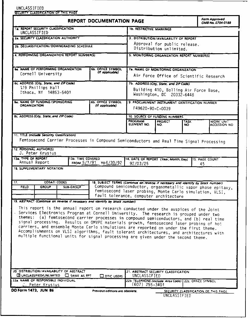
UNCLASSIFIEDSECURITY CLASSIFICATION OF THIS PAGE
Form ApprovedREPORT DOCUMENTATION PAGE OMS No. 0704-0188
ia. REPORT SECURITY CLASSIFICATION lb. RESTRICTIVE MARKINGSUNCLASSIFIED
2a. SECURITY CLASSIFICATION AUTHORITY 3. DISTRIBUTION/AVAILABILITY OF REPORTApproval for public release.2b. DECLASSIFICATION/DOWNGRADING SCHEDULE Disribution uliite.Distribution unlimited.
4. PERFORMING ORGANIZATION REPORT NUMBER(S) S. MONITORING ORGANIZATION REPORT NUMBER(S)
6a. NAME OF PERFORMING ORGANIZATION 6b. OFFICE SYMBOL 7a. NAME OF MONITORING ORGANIZATIONCornell University I (If applicl) Air Force Office of Scientific Research
f6i. ADDRESS (City, State, and ZIP Code) 7b. ADDRESS (City, State, and ZIP Code)119 Phillips Hall Building 410, Bolling Air Force Base,Ithaca. NY 14853-5401 Washington, DC 20332-6448
$a. NAME OF FUNDING/SPONSORING 8b. OFFICE SYMBOL 9. PROCUREMENT INSTRUMENT IDENTIFICATION NUMBERORGANIZATION (If applicable)j ____________ F49620-90-C-0039
8c. ADDRESS (City, State, and ZIP Code) 10. SOURCE OF FUNDING NUMBERSPROGRAM PROJECT FTASK WORK UNITELEMENT NO. NO. NO IACCESSION NO
11. TITLE (Include Security Classification)Femtosecond Carrier Processes in Compound Semiconductors and Real Time Signal Processing
12. PERSONAL AUTHOR(S)J. Peter Krusius
13a. TYPE OF REPORT |13b. TIME COVERED 14. DATE OF REPORT (Year, Month, Day) 15. PAGE COUNTAnnual Report FROM 5/1/91 TO4/30/92 92/03/25 7 45
16. SUPPLEMENTARY NOTATION
17. COSATI CODES 18. SUBJECT TERMS (Continue on reverse if neceasary and identify by block numoer)FIELD GROUP SUB-GROUP Compound semiconductor, organometallic vapor phase epitaxy,
femtosecond laser probing, Monte Carlo simulation, VLSI,fault tolerance, computer architecture
19. ABSTRACT (Continue on reverse if necessary and identify by block number)
This report is the annual report on research conducted under the auspices of the JointServices Electronics Program at Cornell University. The research is grouped under twothemes: (a) femtosecond carrier processes in compound semiconductors, and (b) real timesignal processing. Results on OMVPE materials growth, femtosecond laser probinq of hotcarriers, and ensemble Monte Carlo simulations are reported on under the first theme.Accomplishments on VLSI algorithms, fault tolerant architectures, and architectures withmultiple functional units for signal processing are given under the second theme.
20. DISTRIBUTION/ AVAILABILITY OF ABSTRACT 21. ABSTRACT SECURITY CLASSIFICATIONCM UNCLASSIFEDIUNLIMITED 0 SAME AS RPT CQ OTIC USERS UNCLASSIFIED
22a. NAME OF RESPONSIBLE INDIVIDUAL 22b. TELEPHONE (Include Area Code) 22c. OFFICE SYMBOL. Peter Krusius (607) 255-3401
DO Form 1473, JUN 86 Previous editions are obsolete. SECURITY CLASSIFICATION OF THIS PAGE
UNCLASSIFIED

TABLE OF CONTENTS
A . D irector's O verview ............................................................................................ 1
B. Description of Speciai Accomplishments and TechnologyT ransition ............................................................................................................. 1
B.1 Femtosecond Carrier Processes in Compound
Sem iconductors ....................................................................................... 1
B.2 Real Time Signal Processing .................................................................. 2
C. Description of Individual Work Units ........................................................... 3
C.1 Femtosecond Carrier Processes in Compound Semiconductors
Task #1 OMVPE Growth of HI-V Alloys for New High SpeedElectron D evices .................................................................... 4
Task #2 Femtosecond Laser Studies of Ultrafast Processes in0 Compound Semiconductors ............................................. 13
Task #3 Ultrafast Interactions of Carriers and Phonons inNarrow Bandgap Semiconductor Structures ................ 18
Task #4 Femtosecond Dual Carrier Transport and OpticalInteractions in Compound SemiconducorH eterostructures .................................................................. 21
C.2 Real Time Signal Processing
Task #5 Parallel Structures for Real-Time AdaptiveSignal Processing ............................................................... 30
Task #6 Fault Tolerant Beamforming Algorithms ...................... 35Task #7 Interrupt and Branch Handling for Real-Time Signal
Processing Systems ............................................................ 40

1
A. DIRECTOR'S OVERVIEW
This document is the second year annual report of the Cornell JointServices Electronics Program for the period from May 1, 1990 to April 30, 1993.The present Cornell program carries two themes: femtosecond carrierprocesses in compound semiconductors, and real time signal processing. Theprogram has advanced according to the plan. Eight task investigators, Profs.R. Shealy, C. Tang, C. Pollock, P. Krusius, G. Bilardi, F. Luk, A. Bojanczyk, andH. Torng, with their graduate students have contributed to JSEP research thisyear. Early during this year G. Bilardi left Cornell University in order to takea position at the Italian University, Universita' di Padova, Dipartimento diElecttrotechnica ed Informatica. A substitute task proposed by Prof. AdamBojanczyk was approved starting September 30, 1991. The integration ofresearch under each of the two themes has progressed according to plan andjoint publications are appearing. Eleven graduate students have beenpartially, or fully, supported by JSEP this year. A total of 29 publications andeight theses were prepared in this period and are now various stages ofprocessing. Eight PhD degrees have been awarded to JSEP supported studentsduring this reporting period.
B. DESCRIPTION OF SPECIAL ACCOMPLISHMENTS AND TECHNOLOGYTRANSITION
B.l. Femtosecond Carrier Processes in Compound Semiconductors
Several significant achievements have been reached in the researchperformed under the compound semiconductor theme. The new off-campusorganometallic vapor phase epitaxial (OMVPE) compound semiconductormaterials growth facility has been completed and outstanding OMVPE filmshave been grown under the leadership of R. Shealy. The facility has a totalarea of 5,000 sq ft, with 1,800 sq ft of class 10,000 clean room, and will house 3OMVPE reactors, the first of which became operational during this reportingperiod. The facility design sets new standards in New York State for handlinghighly toxic hydride process gases by exceeding even the stringent code set bythe State of California. Undoped GaAs films have been grown in this multi-chamber OMVPE reactor using triethylgallium (TEG) and arsine source gaseswith at very low V/I flow ratios. Films grown above 600 C are n-type and
have carrier concentrations typically less than 5x10 14 cm-3 with 77K mobilitiesexceeding 101,000 cm 2 /V-s. The second OMVPE reactor is being readied fordeep UV stimulated selective OMVPE growth for exciting new structures.Very high average power of high repetition rate femtosecond pulses in theblue have for the first time been generated by C. Tang's group via intra-cavitydoubling of a mode-locked Ti:sapphire laser using a BaB204 crystal. The samegroup has also set-up a hot luminescence based sensitive time-resolvedspectrometer. This technique has been used to study the relaxation dynamicsof hot carriers in III-V compound semiconductors. C. Pollock's group hasperfected its unique tunable color center laser based femtosecond pump-and-
2
probe characterization system for narrow band gap semiconductors. Carrierrelaxation data for excitations from the band edge up to a few optical phononenergies in InGaAs thin films is being measured. The Monte Carlosimulation group of J. P. Krusius has completed the dual carrier code for the 0time-dependent simulation of non-equilibrium transport in two-dimensional heterostructure devices, such as heterojunction bipolartransistors. In parallel this group has been collaborating with C. Pollock'sefforts to develop and analyze the femtosecond pump-and-probemeasurements on narrow band gap semiconductors. Most recently the ability 0to model the effect of dynamic screening on carrier-optical phonon andcarrier-carrier scattering has been added. A qualitative agreement betweentheory and experiment for InGaAs thin films has been reached.
The Optoelectronics Technology Center (OTC), established inSeptember 1990 under DARPA support, with primary participant fromCornell University, University of California Santa Barbara, and University ofCalifornia San Diego is in its second year. C. Tang continues as one of theleaders of this multi-university program. The Cornell part of the OTCproposal leveraged past JSEP research. The OTC had its first annual reviewmeeting at Cornell University in October 1991. In addition to C. Tang, R.Shealy, C. Pollock, and P. Krusius of the JSEP investigators, are involved inthe OTC research program.
Further special accomplishments are listed in the description ofresearch under each of the tasks.
B.2 Real Time Signal Processing
The investigators involved in the real time signal processing theme,Profs. G. Bilardi, A. Bojanczyk, F. Luk, and H. Torng, have continued thesynergistic work. F. Luk's group discovered the relationship between theBerlekamp-Massey algorithm for decoding the Reed-Salomon code and thewell known Lanczos algorithm. H. Torng's group has made significantprogress in the instruction issuing mechanism, interrupt handling, branchprediction and multi-stream processing, all problems arising in efforts todesign faster superscalar computing machines. While A. Bojanczyk is new tothis group, he will bring a more hardware oriented approach and longer termimpact the program considerably.
H. Torng organized the third "Project 2000" meeting in June 1991 atCornell to report on computer engineering advances in the past year. About15 industrial representatives attended this two day meeting. F. Luk organizedan SPIE meeting on advanced signal processing algorithms, architectures, andimplementations. The proceedings, which he edited, included 46 papers andcovered 494 pages. F. Luk together with A. Bojanczyk were awarded a Warpcomputer by DARPA. This GE built machine was installed at the CornellEngineering and Theory Center building in September 1990. Also a group of

3
INMOS transputers has been installed at the E&TC for exploratorycomputation.
0 Further special accomplishments are listed in the description ofresearch under each of the tasks.
C. DESCRIPTION OF INDIVIDUAL WORK UNITS
C.1 Femtosecond Carrier Processes in Compound Semiconductors
Task #1 OMVPE Growth of HI-V Alloys for New High SpeedElectron Devices ........................................................................ 4
Task #2 Femtosecond Laser Studies of Ultrafast Processes inCompound Semiconductors ................................................ 13
Task #3 Ultrafast Interactions of Carriers and Phonons inNarrow Bandgap Semiconductor Structures .................... 18
Task #4 Femtosecond Dual Carrier Transport and Optical0 Interactions in Compound Semiconductor
H eterostructures ...................................................................... 21
C.2 Real Time Signal Processing
Task #5 Parallel Structures for Real-Time AdaptiveSignal Processing .................................................................... 30
Task #6 Fault Tolerant Beamforming Algorithms ......................... 35Task #7 Interrupt and Branch Handling for Real-Time Signal
Processing System s .................................................................. 40
4
OMVPE GROWTH OF III-V ALLOYS FOR NEWHIGH SPEED ELECTRON DEVICES
Task #1
Task Principal Investigator: James R. Shealy(607) 255-4657
The program objective for the materials task is to explore the use of OMVPEto produce novel epitaxial structures for new high speed electron devices. Theemphasis is to extend the capabilities of the OMVPE process to include sub-micron selective growth of high mobility electron channels, as well as, to useconventional OMVPE techniques to produce high quality III-V alloys, bothlattice matched and pseudomorphic, for the device fabrication and carrierrelaxation studies ongoing in other related JSEP program tasks (2-4). Theprogram objectives are currently proceeding in a series of stages involving theoperation of the new OMVPE facility at Cornell (which includesenvironmental testing) , the construction of an additional OMVPE reactor forthe selective growth studies, and the development of advanced opticalprobing techniques for the non-destructive characterization of 2 dimensionalepitaxial structures.
DISCUSSION OF STATE-OF-THE-ARI
The following discussion of the state-of-the-art is organized into separatesections on photo-stimulated selective OMVPE, the properties of phonons instrained semiconductor short period superlattices, and the operation of a safeOMVPE process with hydrides.
Selective OMVPE Deposition with Deep UV Radiation
Deep UV photo-assisted OMVPE growth is one of the most promising pathsto realizing in situ submicron selective growth. The proposed approach forselective OMVPE on the submicron scale utilizes tunable, coherent deep UVradiation in contrast to all previous attempts. The reactants used in OMVPEare generally transparent in the visible and infrared portion of the spectra.Optical activation of the growth has been achieved using visible laserradiation, where the reactants on the growth surface are not directly excited.The growth is apparently activated by local thermal heating or by carriergenerations near the growth surface [1]. These intermediate steps will mostlikely prevent a high resolution selective growth process due to thermaland/or carrier diffusion prior to the activation of the growth. The deep UVapproach also has its limitations. Previous studies using an ArF excimer laser
5
excitation (193 nm) have found at best a 2:1 growth ratio in theilluminated:dark regions of the substrate. Also, substantial carbonconcentrations [@ (1017) cm- 3 ] are observable in the selectively depositedGaAs films [2]. The laser enhanced growth was found to be severely limited byabsorption in the gas phase. In spite of this, enhanced growth was obs( rvedusing 10 Hz pulse trains with energies as low as 10 mJ/cm2 /pulse withtrimethylgallium (TMG) and arsine.
With other approaches, a visible laser stimulated Atomic Layer Epitaxial(ALE) process, the selectivity has been dramatically improved [3].Unfortunately, this process suffers from limited dimensional control for thereasons stated above and considerable carbon contamination. In all previousstudies the dimensional resolution of the selective growth process (bestlinewidth) exceeds 10 m.
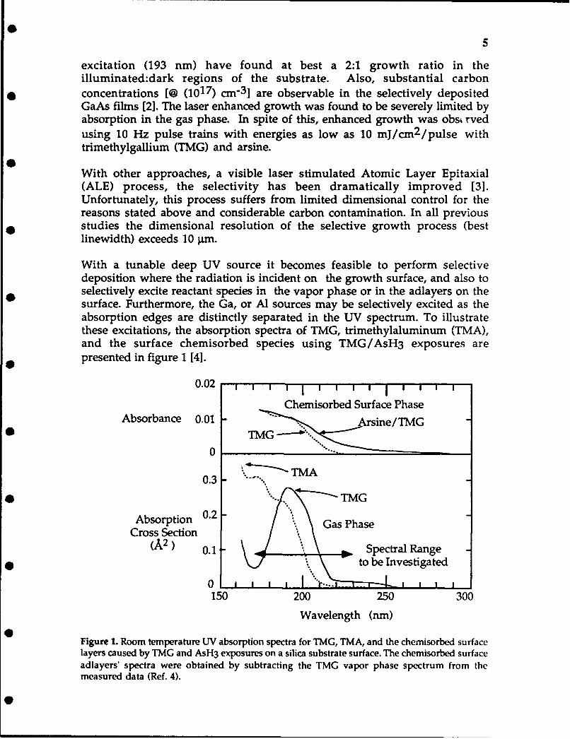
With a tunable deep UV source it becomes feasible to perform selectivedeposition where the radiation is incident on the growth surface, and also toselectively excite reactant species in the vapor phase or in the adlayers on thesurface. Furthermore, the Ga, or Al sources may be selectively excited as theabsorption edges are distinctly separated in the UV spectrum. To illustratethese excitations, the absorption spectra of TMG, trimethylaluminum (TMA),and the surface chemisorbed species using TMG/AsH3 exposures arepresented in figure 1 [4].
0.02 i I
Chemisorbed Surface PhaseAbsorbance 0.01 Arsine/TMG
*TMG -"'.
0
TMA0.3 -
'- . '" TMG
Absorption 0.2 - Gas PhaseCross Section(A2) 0.1 Rag
W Spectral Range* . to be Investigated
0
150 200 250 300
Wavelength (nm)
Figure 1. Room temperature UV absorption spectra for TMG, TMA, and the chemisorbed surfacelayers caused by TMG and AsH3 exposures on a silica substrate surface. The chemisorbed surfaceadlayers' spectra were obtained by subtracting the TMG vapor phase spectrum from themeasured data (Ref. 4).
6
As is evident in figure 1, at an excitation wavelength of 220 nm, the surfacephase may be excited without appreciable absorption in the vapor phase. Notethat previous studies using 193 nm excimer laser radiation resulted inexcitation of both the vapor and surfaces phases, a problem which was cited todegrade the stimulated growth rate and the dimensional selectivity of theprocess[21. The tunable deep UV source (frequency doubled, excimer pumped,dye laser system) will allow the use of coherent radiation from 170 to 220 nm.By selecting the laser wavelength, it becomes feasible to selectively excite theGa or Al vapor species using TMG and TMA by operation at 170 and 210 nm,respectively. These experiments may allow a modulation in the alloycomposition x in AlxGal-xAs films under the proper growth conditions. Itshould be noted that the absorption feature for the TMA vapor near 175 rum isdue to the presence of the dimer species (not seen with TMG) whichtransports near room temperature from the bubbler. As the vapor heats in theboundary layer above the substrate, where the photo-excitation takes place,the dimer species partial pressure is substantially reduced (observed 5y adiminishing 175 nm absorption feature). This may prevent selectiveexcitation of the TMA on or near the substrate surface. For the bestdimensional control however, it appears that for wavelengths longer than220 ram will offer the advantage of a transparent vapor over the substrate.
Phonons in Short Period (AlAs)(InAsl and (GaAs)(InAs) Superlattices
The use of strained layer, short period superlattices has been considered anattractive alternative for conventional lattice matched bulk ternary layers inheterostructure devices. Possible attributes of the superlattice approach arelower thermal spreading resistance of laser cladding layers and improvedimpurity activation, especially in n-type high bandgap alloys.
The most straight forward implementation of this concept has been using(AlAs)(GaAs) structures in heterostructure lasers emitting in the IR [5] andthe visible [6]. In the former study, graded index regions are synthesized withgraded superlattice periods and selectively doped cladding layers are used. Thevisible laser structures have benefited from superlattice active regions asdemonstrated by a reduction of laser threshold currents at wavelengths asshort as 680 nm.
More recently, strained layer superlattices latticed matched (nominally) to InPhave been studies in the (GaAs)(InAs) system [7]. Improved structural andoptical properties are associated with structures produced by MigrationEnhanced Epitaxy (MEE). Besides their potential device applications, theseshort period strained layer structures are interesting from a fundamentalviewpoint. Phonons and electrons in layered media display the effects of zonefolding and quantum confinement which are, in turn, sensitive indicators ofmaterial structure and quality. Depending on the nature of the bulkdispersion in each region of a superlattice the resulting vibrational modes areeither confined or propagative as. In all cases, the acoustic branches fold in the

7
superlattice, giving rise to new Raman active phonons at the reduced zonecenter. These modes are commonly observed to be as sensitive a measure of
* periodicity as X-ray rocking curves of TEM diffraction data. It is interesting tonote that where the optical branches overlap, folding of the optic branchesoccur indicating propagative modes. The region of overlap is substantiallyincreased in the (GaAs)(InAs) case if strain corrections are included in a 1Dlinear chain calculation.
Safety Issues Concerning the OMVPE Process Using Hydrides
A few significant features commonly found in the OMVPE process andrelated facilities are described here. Also the latest N.Y. State guidelines (as setby their Department of Environmental Conservation - DEC) for err sionsinto the environment are given to indicate the need for good process controlfrom the arsine source to the exhaust stack. Most of the information given isobtained through private communications and, as a result, is not referenced.
Generally, conventional vented gas cabinets are used to house the hydride* tanks which are fitted with a flow limiting orifice. If vented gas cabinets are to
be used, dilution exhaust flow required to meet the 1/2 ImmediatelyDangerous to Human Life (IDLH) toxicity level as required the Californiabuilding code are over 35,000 and 300,000 cfm for arsine cylinders with andwithout a standard flow limiting orifice. It should be noted that no arsine
* installation in the U.S. meets the 1/2 IDLH requirement when a catastrophiccylinder failure occurs and few can handle the controlled release through theorifice. New technology is needed to allow the OMVPE technique to be usedin production environments in the near future. Furthermore, recent changesin the DEC code in N.Y. State are more stringent than the California code. For
• example, the ambient guide line concentrations for arsine emissions into theenvironment are 6.5(10-2) and 7.4(10-5) parts per billion (ppb) for short termrelease (1 hour) and annual averages, respectively. These numbers are manyorders of magnitude less than the TLV value of 50 ppb. This requires thatspills be contained and the exhaust from reactors be treated prior to release up
0 the stack. An approach taken at Cornell will be described in the discussion ofprogress below.
It is worth noting that the use of ethyl-organometallic sources generallyreduce the amount of hydride consumption by as much as 2 orders of
• magnitude for acceptable quality films. As a result, a safer OMVPE processemerges using ethyl sources. For example, workers have reported high purityGaAs grown at 10 torr using triethylgallium (TEG) and arsine with a V/IIIratio of unity [8]. Recent results on low V/HI ratios used in GaAs growth willbe presented below.
8
In this section, progress on the OMVPE growth and characterization ofundoped GaAs is presented, as well as, the MEE growth and characterizationof GaInAs and AlInAs structures. A brief update on the status of the selectivegrowth reactor and the deep UV laser system will follow. Finally, a discussionof the the secondary hydride containment system in use in the OM'vPEfacility and results on stack testing are presented.
SOMVPE Growth of Undoped GaAs
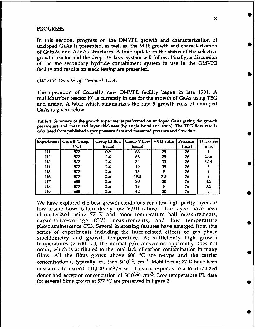
The operation of Cornell's new OMVPE facility began in late 1991. Amultichamber reactor [91 is currently in use for the growth of GaAs using TEGand arsine. A table which summarizes the first 9 growth runs of undopedGaAs is given below.
Table 1. Summary of the growth experiments performed on undoped GaAs giving the growthparameters and measured layer thickness (by angle bevel and stain). The TEG flow rate iscalculated from published vapor pressure data and measured pressure and flow data.
Experiment Growth Temp. Group Ill flow Group V flow V/IH ratio Pressure Thickness('C) (sccm) (sccm) (torr) (mm)
II 577 0.9 66 75 76 1112 577 2.6 66 25 76 2.46113 5,7 2.6 34 13 76 3.14114 577 2.6 49 19 76 6115 577 2.6 13 5 76 3116 577 2.6 19.5 7.5 76 3117 635 2.6 80 30 76 4.5118 577 2.6 13 5 76 3.5I19 635 2.6 42 20 76 6
We have explored the best growth conditions for ultra-high purity layers atlow arsine flows (alternatively low V/II ratios). The layers have beencharacterized using 77 K and room temperature hall measurements,capacitance-voltage (CV) measurements, and low temperaturephotoluminescence (PL). Several interesting features have emerged from thisseries of experiments including the inter-related effects of gas phasestochiometry and growth temperature. At sufficiently high growthtemperatures (> 600 'C), the normal p/n conversion apparently does notoccur, which is attributed to the total lack of carbon contamination in manyfilms. All the films grown above 600 0C are n-type and the carrier
concentration is typically less than 5(1014) cm - 3 . Mobilities at 77 K have beenmeasured to exceed 101,000 cm2 /v sec. This corresponds to a total ionized
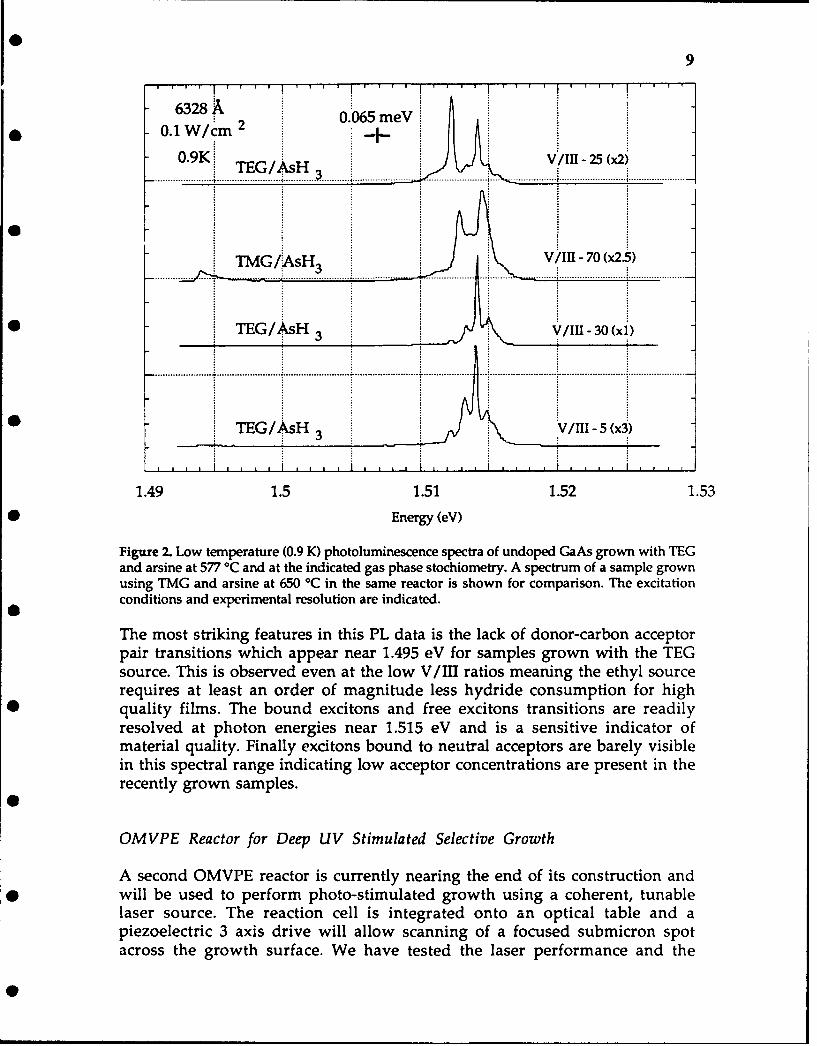
donor and acceptor concentration of 5(1014) cm "3 . Low temperature PL datafor several films grown at 577 'C are presented in figure 2.
9
. .. I . . . . . I ' . . . . . . . . . . . . .
0.065 meV0.1 W/cm 2 i-
0.9KG V/III - 25 (x2)...................... . ............... ..... ................. . ........... .. ... ..................... .. ............. . .................
TMG /AsH V/II -70 (x25)7-V....................* ~TEG/AsH ____V/Il -30 (x1)
-........... .................... ................... ................... ......... ..... ......... ................. .......................... ..................... -
TEG/AsH 3 v/I - 5 (x3)
1.49 1.5 1.51 1.52 1.53
Energy (eV)
Figure 2. Low temperature (0.9 K) photoluminescence spectra of undoped GaAs grown with TEGand arsine at 577 0C and at the indicated gas phase stochiometry. A spectrum of a sample grownusing TMG and arsine at 650 °C in the same reactor is shown for comparison. The excitationconditions and experimental resolution are indicated.
The most striking features in this PL data is the lack of donor-carbon acceptorpair transitions which appear near 1.495 eV for samples grown with the TEGsource. This is observed even at the low V/HI ratios meaning the ethyl sourcerequires at least an order of magnitude less hydride consumption for highquality films. The bound excitons and free excitons transitions are readilyresolved at photon energies near 1.515 eV and is a sensitive indicator ofmaterial quality. Finally excitons bound to neutral acceptors are barely visiblein this spectral range indicating low acceptor concentrations are present in therecently grown samples.
OMVPE Reactor for Deep UV Stimulated Selective Growth
A second OMVPE reactor is currently nearing the end of its construction andwill be used to perform photo-stimulated growth using a coherent, tunablelaser source. The reaction cell is integrated onto an optical table and apiezoelectric 3 axis drive will allow scanning of a focused submicron spotacross the growth surface. We have tested the laser performance and the
10
results look encouraging. When the dye laser is pumped at 25 Hz, the averagepower of the second harmonic exceeds 80 mW (1.7 mJ/pulse) and is tunableover the spectral range from 230 to 255 nm with peak power available at 240nm. This performance is expected to allow excitation of the surface reactantswithout absorption in the gas phase at sufficient energy to stimulate thegrowth over 1 cm 2 areas. This projection is based on data from reference 2and the absorption spectra in figure 1. The first selective growths are plannedfor late summer in 1992.
Test Results on Arsine Containment and Emissions
The arsine cylinders are housed in a secondary containment system whichhas fully pressure tested at the extreme limits of its intended use. Thesecontainment systems (one for arsine, one for phosphine) are now able tohandle a catastrophic cylinder failure. The exhaust from this containmentsystem and from the reactor is passed through a high temperature incineratorfor destruction of residual arsine. We have been monitoring arsine emissionson the exhaust stack since the first run of the multichamber OMVPE reactor.The level of detection is less than 3 ppb prior to dilution and dispersion at thetop of the stack. After the first several runs it was found that the incineratorrequired modifications to meet emission standards. Oxygen/air mixtures areused to insure complete combustion of hydrogen and arsine. The proceduresused for each growth experiment were modified to eliminate "spikes" ofarsine at the beginning and end of each run. We (including a representativefrom the DEC) are able now to observe undetectable emissions throughout agiven growth run. Given the 104 dilution which occurs at the stack and thelevel of detection, Cornell's lab meets the most stringent environmentalprotection standards. Some aspects of the design are currently underconsideration for a patent application. 0
SCIENTIFIC IMPACT OF RESEARCH
The scientific impact of this research task can be summarized in two majorpoints. First, an OMVPE facility can be designed and implemented to insure aminimal level of risk to personnel, the general public and the environment.Furthermore, using certain combinations of organometallic precursors, theamount of arsine consumption is substantially reduced. The PL data on filmsgrown with low arsine anf TEG show the absence of acceptors, in particularcarbon and zinc, which is commonly found in OMVPE materials. When usedin combination with a new Al precursor, trimethylamine alane, we anticipatehigh quality Al containing alloys can be grown in the near future. Second, thedevelopment of the submicron selective OMVPE growth process, using ahigh power deep UV coherent source, will potentially revolutionize thedevelopment of III-V based integrated circuits including those withoptoelectronic elements. The laser system is commercially available and canbe readily integrated into an OMVPE reaction cell to stimulate the reactionson the growth surface without photo decomposition in the vapor phase.
11
DEGREES AWARDED
0 1. Steve O'Brien"Interdiffusion of II-V Semiconductor Quantum Well Heterostructureand its Application to Integrated Electro-Optical Devices"PhD, Electrical Engineering, January 1991
* 2. James Singletery"Promising Solutions to Indium Phosphides Low Schottky Barrier"PhD, Electrical Engineering, May 1991
3. James T. Bradshaw0 "Characterization by Raman Spectroscopy of Graded Index-Separate
Confinement Heterostructure Lasers and Short Period Strained LayerSuperlattices"PhD, Applied Physics, August 1991
* REFERENCES
[1] N.H. Karam, N.A. El-Masry and S.M. Bedair,"Laser Selective Depositionand Direct Writing of Single Crystal HI-V Compound Films," 13thInternational Symposium on Gallium Arsenide and Related
* Compounds Abstracts, Las Vegas, Nevada., (1987), 171-6.
[2] P. Balk, M. Fischer, D. Gundmann, R. Luckerath, H. Luth and W.Richter, "Ultraviolet-Assisted Growth of GaAs," J. Vac. Sci. Technol.,B5(1987), 1453-9.
0[31 S.P. DenBaars, P.D. Dapkus, C.A. Beyler, M. Zandian, A. Hariz, and K.
Dzurko," Thermal and Laser Assisted Atomic Layer Epitaxy ofCompound Semiconductors,"15th International Symposium onGallium Arsenide and Related Compounds Abstracts, Atlanta, Ga.,
* (1988), 60-1.
[4] M.Sasaki, Y. Kawakyu, H. Ishikawa, and M. Mashita, "UV AbsorptionSpectra of Adlayers of MOCVD Source Gases," Appi. Surface Sci., 41/42(1989), 343-45.
0 [51 J.R. Shealy, "High-Efficiency Superlattice Graded-Index SeparateConfining Heterostructure lasers with AlGaAs Single Quantum Wells,"Appl. Phys. Lett., 52 (1988), 1455-7.
[61 T. Hayakawa, T. Suyama, K.Takahashi, M. Kondo, S. Yamamoto, and T.Hijikata, "Low Current Threshold A1GaAs Visible Laser Diodes with an(AlGaAs)m(GaAs)n Superlattice Quantum Well," Appl. Phys. Lett., 49(1986), 636-8.
0
12
[7] J.M. Gerard, J.Y. Marzin, B. Jusserand, F. Glas, J. Primot, "Structural andOptical Properties of High Quality InAs/GaAs Short-Period SuperlatticesGrown by Migration-Enhanced Epitaxy," Appl. Phys. Lett., 54 (1989), 30-2.
[8] K. Kimura, S. Takagishi, S. Horiguchi, K. Kamon, M. Mihara and M.Ishii, "Low Pressure OMVPE Growth of GaAs Using TEG," lap. Jour.Appl. Phys., 25 (1986), 1393-6.
[9] J.R. Shealy, "Characterization of AlGaAs/GaAs Heterostructures Grownin a Multichamber OMVPE Apparatus," J. Crystal Growth, 87 (1988), 350-356.
ISEP PUBLICATIONS S
1. "Monolithic Integration of an (Al)GaAs Laser and an IntracavityElectroabsorption Modulator Using Selective Partial Interdiffusion," S.O'Brien, J. R. Shealy, and G. W. Wicks, Appl. Phys. Lett., 58 (13), April 1,1991.
2. 'Tunable (Al)GaAs Lasers Using Impurity-Free Partial Interdiffusion," S.O'Brien, J. R. Shealy, F. A. Chambers, and G. Devane, 1. Appl. Phys., 71 (2),January 1992.
3. "Characterization by Raman Scattering X-Ray Diffraction andTransmission Electron Microscopy of (AlAs)m(inAs)m Short PeriodSuperlattices Grown by Migration Enhanced Epitaxy," J. Bradshaw, X. J.Song, J. R. Shealy, and H. Ostergaard, to appear in J. Appl. Phys.
0
13
FEMTOSECOND LASER STUDIES OF ULTRAFAST PROCESSES IN
COMPOUND SEMICONDUCTORS
Task #2
Task Principal Investigator. C. L Tang(607) 255-5120
* The objective of this task is to develop new femtosecond sources andmeasurement techniques and to use such sources and techniques to studyultrafast processes in compound semiconductors and related structures. Onsource development, current emphasis is on high repetition rate all-solid-state femtosecond sources and in extending the tuning range of such sources.
0 On optical measurement techniques, current emphasis is on developingoptical sampling techniques with femtosecond time resolution based the up-conversion processes. These sources and techniques are being successfullyapplied to studying the relaxation dynamics of non-equilibrium carriers in HI-V compounds and quantum wells. The capture problem and the problem of
0 tunneling of coherent wave packets in quantum wells are of particularinterest at the present time.
DISCUSSION OF THE STATE-OF-THE-ART
0 Almost all the work on femtosecond optics and ultrafast processes in the pasthas been based on the use of the mode-locked Rh6G femtosecond dye laser asthe primary source of short pulses of light. The trend recently has been tomove away from the dye lasers to all-solid-state short pulse sources. CWmode-locked Ti-doped sapphire laser has been most widely used new primaryfemtosecond laser source. The Ti:sapphire laser is tunable over the range of720 nm to about 1 mm. The emphasis of our work has been to extend theuseful range of all-solid-state femtosecond lasers to beyond this range throughnonlinear optical techniques. Very significant progress has been made in thiseffort during the past year and the results are discussed below in the Progresssection.
In the case of femtosecond optical measurement techniques, most of the paststudies of ultrafast phenomena have been based upon some sort of pump-probe measurement, including the related correlation spectroscopictechniques. All these techniques suffer from the fact that during the probingprocess, the system being measured is also disturbed to some extent. To avoidperturbing the system being measured, the time-resolved hot luminescenceup-conversion technique has been developed to study the relaxation
14
dynamics of non-equilibrium carriers in semiconductors at a number oflaboratories recently, including Cornell. This technique allows opticalsampling with a time resolution on the order of 50 fs of the very weak hotluminescence emitted by the carriers during the relaxation process. Thistechnique has now been well developed where the dark noise count is downto half a photon per second and has been used successfully to yieldunambiguous data on the cooling rates of hot carriers in bulk GaAs andGaAs/AlGaAs quantum wells at high carrier densities. An earliercontroversy on this issue is thus resolved unambiguously and put to rest.
The relative hot-electron cooling rates for bulk and quantum well (QW)structures is an important, basic question that affects many applications ofquantum well structures and has inspired a large number of theoreticalstudies. It is well known that the hot-carrier cooling rate decreases withincreasing carrier concentration in both QW and bulk structures. The firststudy comparing GaAs/AlGaAs QW's and bulk GaAs reported similarcooling rates at a carrier density (n) of 2.5x10 17 am- 3 [1]. Subsequent studiesreported a much slower cooling rate in QW's than in the bulk at highercarrier densities (n>10 1 8 cm - 3 ) [2-51. Nevertheless, in a number of recentpublications Leo et al. [6, 7] have cited these previous results as beingcontradictory and concluded that the cooling rates of bulk GaAs andGaAs/AlGaAs QW's are equivalent. These comparisons, however, werebased on comparisons limited to the carrier density range of 101 5 <n<10 1 8
cm "3 , generalizing that the independence of carrier cooling withdimensionality is also independent of carrier density. The former studies [2-51were carried out using nonlinear intensity correlation spectroscopy. Thelatter study was carried out using a time-resolved streak-camera with a timeresolution of -20 ps. Using the more accurate time-resolved hot-luminescence spectroscopic technique we have now shown conclusively [81that the cooling rates of the quantum-well structures are significantly slowerthan that of the bulk for n>5x10 18 cm -3 and similar at 2x1018 cm "3 or lowerthus confirming the earlier observations [2-51 of the difference in the coolingrates between the bulk and quantum well structures. This difference couldnot have been seen in the carrier density range studied by Leo et al. [7, 8]. 0
PROGiRESS
High repetition rate femtosecond pulse generation in the blue [9] - We havesucceeded in generating very high average powers of high repetition rate Sfemtosecond pulses in the blue for the first time by intracavity doubling of amode-locked Ti:sapphire laser using b-BaB204 (BBO). To reduce the pulsebroadening effect of group velocity mismatch, an extremely thin BBO crystalis used. Pumping the Ti:sapphire laser with 4.4 W from an Ar + laser, up to230 mW of 430 nm light is produced at 72 MHz repetition rate and 89 fspulsewidth. This represents an effective conversion efficiency of -75% fromthe typical infrared output to the second harmonic. Pulse widths as short as
15
54 fs are achieved for the blue output. Recent conversion to a higher powerAr+ laser pump has led to blue output in the range of 400 mW. We expect
*1 eventually to reach the 1 W level. When this is reached, we expect to be ableto generate femtosecond uv pulses near 200 nm at a substantial power level,which should open up many ultrafast processes in a variety of materials andstructures for study in the femtosecond time domain. Work is also underway to achieve extra-cavity pumping of the femtosecond OPO by theTi:sapphire laser. This should make it much easier for others to operate the fsOPO's than in the case of intracavity pumped OPO demonstrated by us earlier.; is should open up the broad mid ir range up to 4.5 mm for studies in thefemtosecond time domain by many laboratories.
Hot luminescence spectroscopy [9] - A very sensitive time-resolvedupconversion spectroscopic setup has been built in our laboratory. This time-resolved spectrometer has a time resolution on the order of 50 fs, spectralrange from approximately 400 nm to 2.5 mm, and noise of 0.5 Hz. It has beensuccessfully used to study the relaxation dynamics of hot carriers in III-Vcompounds and will be applied to the quantum well carrier-capture problem
* and the coherent electron-wavepacket tunneling problem.
Comparison of hot-carrier relaxation in quantum wells and bulk GaAs athigh carrier densities [8] - An investigation of the hot-carrier relaxation inGaAs/(A1,Ga)As quantum wells and bulk GaAs in the high-carrier-density
* limit is completed. Using a time-resolved luminescence up-conversiontechnique with < 80 fs temporal resolution, carrier temperatures aremeasured in the 100 fs to 2 nsec range. Our results show that the hot-carriercooling rates in the quantum wells are significantly slower than in the bulkfor carrier densities greater than 2x10 18 cm- 3 . A comparison is made with
* previous publications to resolve the confusion concerning the difference incooling rates in quasi-two and three dimensional systems.
SCIENTIFIC IMPACT OF RESEARCH
0 The femtosecond sources and measurement techniques developed should beof great use to others in the scientific community. The results obtained onthe dynamics of nonequilibrium carriers in III-V compounds and structuresare of fundamental importance to the understanding of the physics and thedesign of ultra-high speed semiconductor electronic and optical devices.
DEGREES AWARDED
1. E. S. Wachman"Ultrafast spectroscopy with a novel broadly tunable cw femtosecondsource"PhD, Applied Physics, 1991.
2. W. H. Loh
16
"Polarization Self-Modulation in Semiconductor Lasers"PhD, Electrizal Engineering, August, 1991.
3. Y. Ozeki •"Study of two-mode optical bistable semiconductor laser diodes with intra-cavity saturable absorbers"PhD, Electrical Engineering, August, 1991.
REFERENCES S
[1] C. V. Shank, R. L. Fork, R. Yen, J. Shah, B. I. Greene, A. C. Gossard, and C.Weisbuch, Solid State Commun. 47, 981 (1983).
[2] Z. Y. Xu and C. L. Tang, App. Phys. Lett. 44, 692(1984). S
[3] H. Ukichi, Y. Arakawa, H. Sakaki, and T. Kobayashi, Solid State Comm.55, 311 (1985).
[4] S. A. Lyon, J. Lumm. 35, 121 (1986). 0
[5 A. J. Nozik, C. A. Parsons, D. J. Dunlavy, B. M. Keyes, and R. K.Ahrenkiel, Solid State Comm. 75, 297 (1990).
[61 K. Leo, W. W. Ruhl, and K. Ploog, Phys. Rev. B 38, 1947(1988); Solid. State 0Elect. 32, 1863 (1989).
[7] K. Leo, W. W. Ruhl, H. J. Queisser, and K. Ploog, App. Phys. A 45,35(1988); Phys. Rev. B 37, 7121 (1988).
[81 W. S. Pelouch, R. J. Ellingson, P. E. Powers, C. L. Tang, D. M. Szmyd, andA. J. Nozik, Phys. Rev. B 45, 1450(15 January, 1992); 7th InternationalConference on Hot Carriers Conference in Semiconductors, Nara, Japan,(July, 1991).
[91 "High Repetition Rate Femtosecond Pulse Generation in the Blue," R. J.Ellingson and C. L. Tang, Optics Letters (scheduled for March, 1992); alsoto be presented at CLEO '92, Anaheim, CA ( May, 1992).
ISEP PUBLICATIONS AND TALKS
1. "Broadly tunable cw femtosecond optical parametric oscillators," C. L.Tang, W. Pelouch, and P. Powers, invited talk, CLEO '91, Baltimore, MD(May, 1991).
2. "Polarization bistability in semiconductor lasers," C. L. Tang, Y. Ozeki, •and J. Johnson, CLEO '91, Baltimore, MD (May, 1991).
0
17
3. "Femtosecond optical parametric oscillators," C. L. Tang, invited talk,American Physical Society March Meeting, Cincinnati, OH (March 18-21,1991).
4. "Femtosecond optics," International Workshop on Lasers in Chemistryand Physics, Dalian, China, sponsored by UNESCO and the ChineseAcademy of Sciences (May 22-28, 1991).
5. "CW femtosecond pulses tunable in the near- and mid-infrared," E. W.Wachman, W. S. Pelouch, and C. L. Tang, 1. App. Phys., 70, 1893(1 August, 1991).
6. "Comparison of hot-carrier relaxation in quantum wells and bulk GaAsat high carriers densities," W. S. Pelouch, R. J. Ellingson, P. E. Powers,C. L. Tang, D. M. Szmyd, and A. J. Nozik, Phys. Rev. B 45, 1450 (15January, 1992).
7. "Investigation of hot carrier relaxation in quantum well and bulk GaAsat high carrier densities," W. S. Pelouch, R J. Ellingson, P. E. Powers, C.L. Tang, D. M. Szmyd, and A. J. Nozik, Proceedings of 7th InternationalConference on Hot-Carriers in Semiconductors, Nara, Japan (July 1991).
8. "High Repetition Rate Femtosecond Pulse Generation in the Blue," R. J.Ellingson and C. L. Tang, Optics Letters (scheduled for March, 1992); alsoto be presented at CLEO '92, Anaheim, CA( May, 1992).
9. "Polarization bistability in semiconductor lasers with ir.tracavitymultiple quantum well saturable absorbers", Y. Ozeki, J. E. Johnson, andC. L. Tang, App. Phys. Lett., 58,1958 (1991).
10. "Polarization switching and bistability in an external cavity laser with apolarization-sensitive saturable absorber," Y. Ozeki and C. L. Tang, Appl.Phys. Lett., 58, 2214 (1991).
11. "Dynamics of hot carriers in quantum wells and bulk GaAs at highcarrier densities: femtoseconds to naoseconds," invited talk, SPIEConference on Ultrafast Laser Probe Phenomena in Bulk andMicrostructures in Semiconductors and Superconductors, Somerset, NJ(22-26 March, 1992).
12. "Optical parametric oscillators," C. L. Tang, invited talk, InternationalSchool on Optics and Optical Physics, Capri, Italy (1992).

18
ULTRAFAST INTERACTIONS OF CARRIERS AND PHONONS INNARROW BANDGAP SEMICONDUCTOR STRUCTURES
Task #3
Task Principal Investigator: Clifford Pollock(607) 255-5032
Our goal is to provide experimental data that can be used to confirm or refutethe current models used to describe hot electron relaxation in narrowbandgap semiconductors. In this manner, we are measuring the carrierrelaxation in various samples and providing the results of the measurementsto Prof. Krusius for comparison with his groups simulations of the scatteringprocess.
DISCUSSION OF STATE-OF-THE-ART
Most of the ultrafast work in InGaAs has been on quantum well structures,such as laser diode amplifiers. One motivation for doing femtosecond studiesof diode amplifiers is "gain compression", which refers to a decrease in gain athigh modulation rates. Most pump-probe work on amplifiers attempts tocharacterize this effect. Working in a semiclassical picture (carrier/photonrate equations), one can model the recovery. The debate in the field is aboutthe importance of different forms of carrier relaxation. Spectral hole burninghas been suggested to explain the transient gain decrease. Others advocatecarrier heating: carrier transitions occur away from the bandgap due to thewideband nature of the femtosecond pulses, while stimulated emissionoccurs preferentially at the bandgap [1]. The effect occurs because carriers needto cool down to reach the bandgap and be more readily available forstimulated emission.
Recently, a new candidate for the gain nonlinearity has been proposed. Weiss[21 considered an InGaAs/InGaAsP MQW structure similar to Hall's paperabove. They proposed that spatial transport of carriers from the boundarylayers cladding the MQW structure. The experiments appear identical, thedifference lies in the models used to fit the data by the two groups. Hall usesrate equations with a phenomenological heating term, while Weiss fits thegain decay rate to a carrier diffusion model. A third amplifier gaincompression paper deals with the same issues [3].
Carruthers [4] at NRL examined a vertical stack heterojunction bipolartransistor. He used a modelocked Er-fiber laser to generate 1.6 ps pulses at
19
1.53um. Shining the light on the emitter contact layer (which was the InGaAslayer that absorbed most of the light and injected photocarriers into theInP/InGaAs/InP transistor structure below ), with the collector grounded, theemitter photocurrent was observed with a 40GHz scope. This revealed a 12pselectrical pulse. The author aottributes the width to RC effects, but theexperiment in principle could measure transit times.
Knox [5] laid down parallel stripline on top of the quantum well. A pumpbeam at the appropriate energy to generated excitons which were rapidlyionized by an applied electric field. The electrical transient this generatedpropagated rapidly inside the stripline. Because the exciton creation time isvery fast, and the exciton absorption line is Stark shifted by an E field, theexciton absorption strength was a sensitive measure of the field inside thestripline. Knox used a pump at one end of the line to generate an initialphototransient, and used a probe beam at the same energy but displaced alongthe line to measure the electric field strength, with 100 fs time resolution andlum spatial resolution. He observed signals propagating near the speed oflight (since the QW was very thin, with no substrate, the electrical group
0 velocity is extremely large in these structures).
We found through comparison of data to simulation that an experimental* accuracy and repeatability of I part in 1000 was required. This is not simply a
Signal/Noise issue, but a problem of removing all systematic errors from thedata to this level. The search for systematic errors has been the thrust of mostof our work in the past year.
* Much of the error in our signals was traced to the variable delay arm of thespectrometer. We found that our data was slightly asymmetric, at least on thescale of parts per thousand. The source of the asymmetry was found to lie ina slow creep of the galvonometer that was used to scan the retroreflectingmirror of the delay arm. In response, we improved the galvanometer-driven
* optical delay device by using a lightweight translation stage to insurelinearity, and by using position sensitive feedback to monitor and control thegalvo itself.
We have evaluated several different noise reduction techniques. We foundthat the weak reflection of the pump laser from our femtosecond laser led toamplitude instabilities in the output power, and this caused excess noise inour signal. We implemented a new feedback amplitude stabilizer usingacousto-optic (AO) modulation of the pump for our ultrafast laser. The AOcell both amplitude stabilizes the pump beam, and further it acts as an opticalisolator between the two systems, reducing the deleterious feedback. Inaddition, we have refined the existing feedback control of cavity length.Finally, we have mapped out a larger range of operating parameters of theAPM laser, allowing us to generate a more stable train of femtosecond pulses.
0
420
Our data shows the recovery time of the measured transmission fits a singleexponential decay, which is a simplification of the process, but describes thedata very well. Data is being collected as a function of wavelength, and we arejust setting up a temperature stage to measure the effects of increasedtemperature on the scattering rates.
SCIENTIFIC IMPACT OF RESEARCH
These measurements will provide a test of the models used by designers tosimulate the performance of InGaAs devices. They will be invaluable forrefining and improving present theory and simulation of hot carriers innarrow bandgap materials.
DEGREES AWARDED
None.
REFERENCES
[1] "Femtosecond Gain Dynamics and Saturation Behavior in InGaAsPMultiple Quantum Well Optical Amplifiers," K. Hall, Y. Lai: E. Ippen, G.Eisenstein, U. Koren, APL 57, 27, (1990)
[2] "Carrier Capture Times in 1.5um Multiple Quantum Well OpticalAmplifiers," S. Weiss, J. Wiesenfeld, D. Chemla, G. Raybon, G. Sucha, M.Wegener, G. Eisenstein, C. Burrus, A. Dentai, U. Koren, B. Miller, H.Temkin, R. Logan, T. Tanbun-Ek, APL 60, 1, (1992)
I
[3] "Gain Compression and Recovery Dynamics in Multiple Quantum WellOptical Amplifiers," in Ultrafast Phenomena VII, Springer-Verlag '90, J.Wiesenfeld, G. Eisenstein, M. Wegener, D. Chemla G. Raybon, U. Koren,S. Weiss
[41 "Responses of an InP/InGaAs/InP Heterojunction Bipolar Transistor to1530 and 620 nm Ultrafast Optical Pulses," T Carruthers, I. Duling III, 0.Aina, M. Mattinglv M. Serio, APL 59, 3, (1991)
[5] "Ultrafast Dynamical Response of Quantum Well Excitons in AppliedFields," W. Knox, Workshop on Optical Properties of MesoscopicSemiconductor Structures, Snowbird, Utah, April 1991
SEP PUBLICATIONS
1. "Femtosecond Electron Relaxation in InGaAs Lattice-Matched to InP," D.Cohen and C. R. Pollock, to be presented at SPIE conference 1677, March25, 1992, Somerset, New Jersey.
21
FEMTOSECOND DUAL CARRIER TRANSPORT AND OPTICALINTERACTIONS IN COMPOUND SEMICONDUCTOR
HETEROSTRUCTURES
Task #4
Task Principal Investigator. J. P. Krusius(607) 255-3401
OBJE~nEIY
The objective in this work unit is to explore non-equilibrium carrierprocesses governing electron and hole transport and optical interactions ininhomogeneous compound semiconductor heterostructures theoretically.Electron and hole interactions among themselves, the semiconductor lattice,optical fields, and external electric fields are described using self-consistentensemble Monte Carlo formulations including quantum well phenomena.This work is done collaboratively with femtosecond optical measurementsand materials growth efforts. In the area of femtosecond optical probing withtunable lasers, joint work is performed together with C. Pollock's researchgroup in order to design samples, optical experiments, analyze measured data,and extract microscopic information of femtosecond carrier processes. TwoPhD graduate students, J.E. Bair and S. Weinzierl, have worked on this task inaddition to the principal investigator.
DISCUSSION OF STATE-OF-THE-ART
A variety of ballistic injection cathodes have been built into the structure ofcompound semiconductor devices in order to enhance their high speedperformance. These include the n+/n homojunction [1], the p+/nheterojunction [2], the abrupt heterojunction [3], and the Schottky barrier [4]. Ithas been experimentally demonstrated that these injection cathodes cangenerate a significant quasi-ballistic electron fraction in compoundsemiconductor devices, but despite such observations there is no conclusiveevidence on whether such injection structures substantially increase deviceperformance. The first published observation of the probing of the non-equilibrium electron distribution was made on the planar doped barriertransistor (PDBT), which was used as a hot electron spectrometer [5]. Anotherdevice structure used at about the same time was the tunneling hot electrontransfer amplifier (THETA), first in its vertical form [6] and later in its lateralform [7]. Several attempts to fabricate unipolar FET devices with hot electroncathodes to generate ballistic electrons were also made but results wereambivalent [8, 9]. However, because of the complexity of designing andfabricating three terminal devices with hot electron cathodes, it was not clearwhether fabricated devices suffered from materials growth or processing
22
related non-idealities, incorrect device designs, or the insignificant impact ofballistic electron processes on the terminal characteristics of devices. In orderto resolve these fundamental questions it is necessary to explore themicroscopic physics of the transport in such devices via sophisticatedsimulation techniques, which can resolve the underlying microscopicprocesses, including non-equilibrium carrier transport in inhomogeneousdevices. Consequently a two-dimensional time-dependent self-consistentensemble Monte Carlo method has been developed by this group and used toexamine the impact of the above and many other hot carrier processes on the 0terminal characteristics.
The relaxation of carriers excited by ultra-short optical pulses has beenintensely studied both experimentally and theoretically for several years.Despite this a full understanding of the complex carrier dynamics in thesehighly non-equilibrium situations is still lacking. Current Monte Carlomodels of carrier relaxation have achieved considerable success in explainingmany qualitative features of experimental observations [10, 11]. However, agreat deal of uncertainty remains. At the heart of these uncertainties lies therole of carrier-carrier scattering. Models to this point have almost 0unanimously assumed that free carrier screening can be adequately describedby using long wavelength static approximations. However, recent resultshave indicated carrier-carrier scattering may be seriously underestimated in astatic screening limit [12, 131. Theoretical calculations also have shown thatcarrier-carrier scattering rates are significantly enhanced, if dynamic screeningeffects are taken into account [14, 151. Since the two most important scatteringprocesses in compound semiconductors, polar optic phonon scattering andcarrier-carrier scattering, are both heavily dependent on free carrier screening,this issue is critical in the understanding the role of these scatteringmechanisms. Significant progress must be made in this area before the details 0cf femtosecond optical experiments can be understood. Progress in this areahas recently been made through a joint ensemble Monte Carlo/moleculardynamics approach [16] which has some success in correlating with measureddata. However, this method appears limited to homogenous systems due tolimitations arising from the size of the area that can be simulated. Thus it is 0unlikely that this method can be applied more widely to the modeling ofother highly non-equilibrium phenomena, such as is found in state of thehigh speed compound semiconductor devices.
Non-Equilibrium Carrier Transport
Work in this subtask has built on our past efforts with progress made in thefollowing areas: dual carrier transport formulation and softwaredevelopment, and understanding of carrier launching across electronlaunchers subject to interactions with two-dimensional space charges.
23
The bipolar part of our previous software package, OPTMC developed by J.E.Bair, has been incorporated into the existing 2DMC transport code. The newcode, M2EDUSA, for Multi-dimensional Monte carlo Ensemble Simulationfor Detailed Unipolar and bipolar heterojunction Semiconductor deviceAnalysis, implements a two conduction band k.p band valleys, F-L, and two
hole bands, F, including warping. All the usual scattering mechanisms areincluded. Any number of ternary compound layers, with either donor or
0 acceptor doping, can be specified along one spatial dimension. A materialhomogeneity is assumed in the lateral direction. Either rectangular or mesatype devices can be simulated, and ohmic or Schottky contacts of any lengthcan be placed anywhere around the two-dimensional periphery. Quantummechanical reflection due to the potential step at the abrupt heterojunctions
* is included to first order. The entire implementation was constructed withthe goal of having the simulations run as accurately as possible in aworkstation computing environment without the use of supercomputingresources. This required, for example, the of analytic energy bands in order todecrease run time memory requirements and the exclusion of carrier
* scattering in order to keep execution times acceptable. A typical M2EDUSArun for a vertical FET with an abrupt heterojunction, zero applied bias, chargeneutral initial state, 256x64 point spatial mesh, 50000 particles, and 1000 timesteps takes about 8:45, 2:54, and 2:26 hrs:min on an HP9000/380, a DEC5000/200, and an HP 9000/720 engineering workstation respectively. As a
* calibration, the HP-RISC station 9000/720 is 37.4 times faster than the DECVAX 11/780, an early 1980's CISC computer, which has often been used abenchmark.
M 2EDUSA has been calibrated and verified against physics principles, othersimulators, and experiments. The simulated velocity field curve for GaAsmatched with measured data within the experimental error. M2EDUSAaccurately resolves the transient phenomenon of the formation andpropagation of a stable Gunn domain. M2 EDUSA also accurately models thedynamics of carrier heating and cooling, the time-dependence of the electron
* phonon interaction and the average momentum relaxation time. Thecorrelation of M2EDUSA simulated current-voltage characteristics withmeasured device data for a vertical FET with an imbedded heterojunctionshows an excellent overall agreement. M2 EDUSA wts also used to simulatesignificant characteristics of the homojunction pn diode and the
* homojunction bipolar junction transistor with a direct comparison with thedrift-and-diffusion simulator PISCES-II with excellent results. Furtherverification and calibration studies are documented in detail in S. Weinzierl'sPhD thesis (see degrees awarded).
To date M2 EDUSA has been used to simulate the following unipolar andbipolar compound semiconductor devices: the abrupt vertical field effecttransistor with an abrupt heterojunction launcher, HJ-VFET; the modifiedplanar doped barrier vertical FET transistor (PBD-VFET); and the ballistic
24
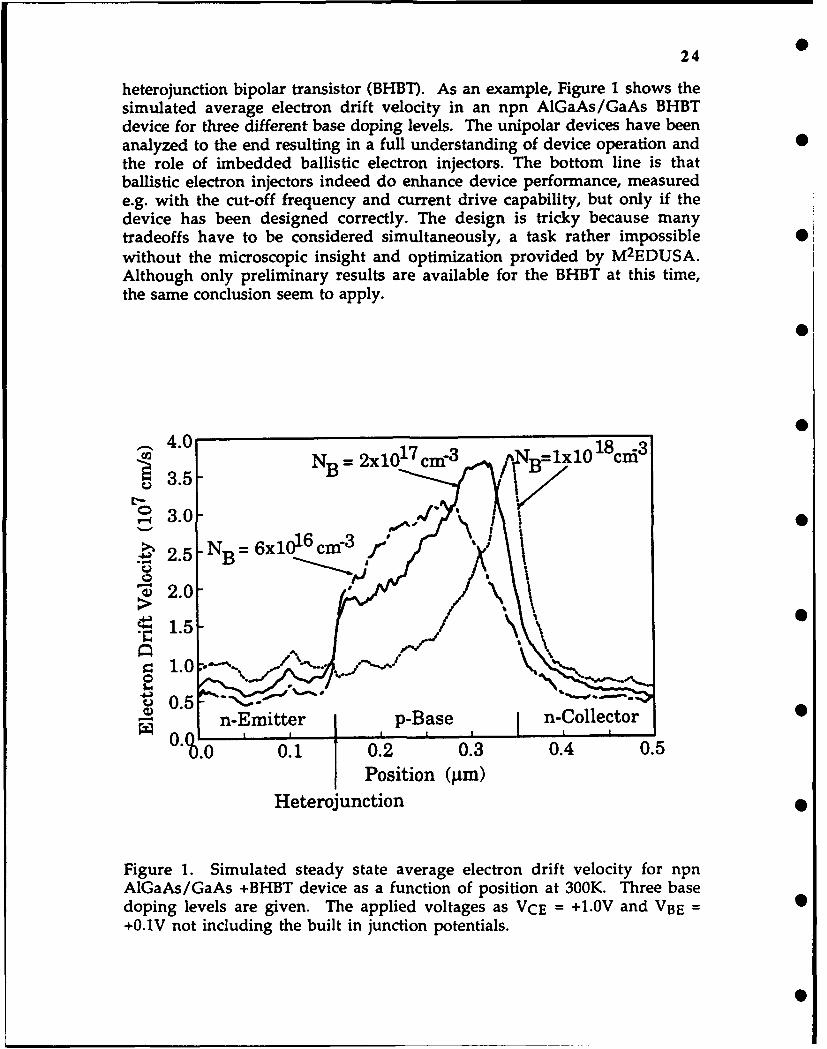
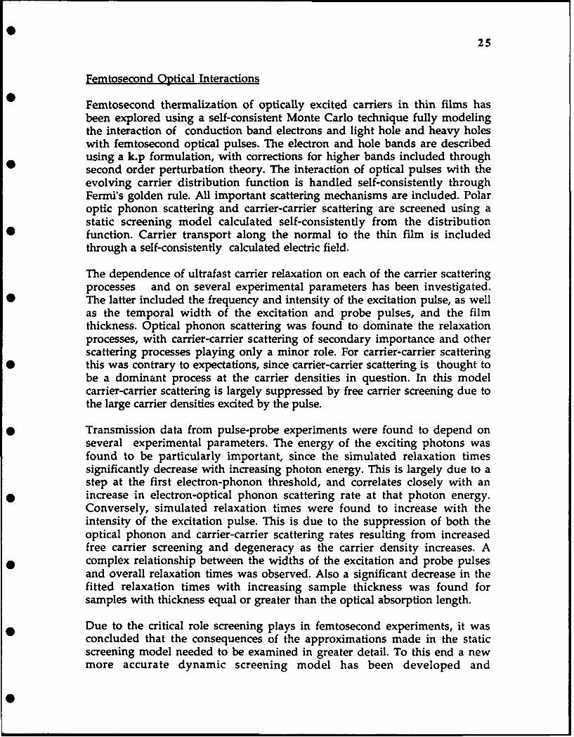
heterojunction bipolar transistor (BHBT). As an example, Figure 1 shows thesimulated average electron drift velocity in an npn AlGaAs/GaAs BHBTdevice for three different base doping levels. The unipolar devices have beenanalyzed to the end resulting in a full understanding of device operation and 0
the role of imbedded ballistic electron injectors. The bottom line is thatballistic electron injectors indeed do enhance device performance, measurede.g. with the cut-off frequency and current drive capability, but only if thedevice has been designed correctly. The design is tricky because manytradeoffs have to be considered simultaneously, a task rather impossible 0
without the microscopic insight and optimization provided by M2EDUSA.Although only preliminary results are available for the BHBT at this time,the same conclusion seem to apply.
4.0 3
N B 2l4.0~3 .,NB: X1O l8C3
3.5 NB- 2x10. c-Vl
S3.0 '
NB6x1016 cm 3 ,f "
UB
.. 2.5 jm /
0 2.0-
e-1.5-o .4%%%1.0,
0.5 " -n-Emitter p-Base n-Collector
.0 0.1 0.2 0.3 0.4 0.5
Position (gm)
Heterojunction
Figure 1. Simulated steady state average electron drift velocity for npnAlGaAs/GaAs +BHBT device as a function of position at 300K. Three basedoping levels are given. The applied voltages as VCE = +I.OV and VBE =
+0.1V not including the built in junction potentials.
25
Femtosecond Optical Interactions
0 Femtosecond thermalization of optically excited carriers in thin films hasbeen explored using a self-consistent Monte Carlo technique fully modelingthe interaction of conduction band electrons and light hole and heavy holeswith femtosecond optical pulses. The electron and hole bands are describedusing a k.p formulation, with corrections for higher bands included throughsecond order perturbation theory. The interaction of optical pulses with theevolving carrier distribution function is handled self-consistently throughFermi's golden rule. All important scattering mechanisms are included. Polaroptic phonon scattering and carrier-carrier scattering are screened using astatic screening model calculated self-consistently from the distribution
* function. Carrier transport along the normal to the thin film is includedthrough a self-consistently calculated electric field.
The dependence of ultrafast carrier relaxation on each of the carrier scatteringprocesses and on several experimental parameters has been investigated.
* The latter included the frequency and intensity of the excitation pulse, as wellas the temporal width of the excitation and probe pulses, and the filmthickness. Optical phonon scattering was found to dominate the relaxationprocesses, with carrier-carrier scattering of secondary importance and otherscattering processes playing only a minor role. For carrier-carrier scattering
* this was contrary to expectations, since carrier-carrier scattering is thought tobe a dominant process at the carrier densities in question. In this modelcarrier-carrier scattering is largely suppressed by free carrier screening due tothe large carrier densities excited by the pulse.
0 Transmission data from pulse-probe experiments were found to depend onseveral experimental parameters. The energy of the exciting photons wasfound to be particularly important, since the simulated relaxation timessignificantly decrease with increasing photon energy. This is largely due to astep at the first electron-phonon threshold, and correlates closely with an
* increase in electron-optical phonon scattering rate at that photon energy.Conversely, simulated relaxation times were found to increase with theintensity of the excitation pulse. This is due to the suppression of both theoptical phonon and carrier-carrier scattering rates resulting from increasedfree carrier screening and degeneracy as the carrier density increases. A
* complex relationship between the widths of the excitation and probe pulsesand overall relaxation times was observed. Also a significant decrease in thefitted relaxation times with increasing sample thickness was found forsamples with thickness equal or greater than the optical absorption length.
Due to the critical role screening plays in femtosecond experiments, it wasconcluded that the consequences of the approximations made in the staticscreening model needed to be examined in greater detail. To this end a newmore accurate dynamic screening model has been developed and
26
implemented in our Monte Carlo code. The new model is derived from theLindhard dielectric function and fully incorporates the energy dependence ofthe free carrier screening. The use of an approximate parabolic band structureand neglecting anisotropy for the bands, carrier distributions, and dielectric 0function are the only simplifications made. Improvements are beingconsidered to incorporate a more accurate band structure with anisotropy intothe model.
The new dynamic screening model resulted in a dramatic change in the effect 0of free carrier screening. Polar optical phonon scattering appears largelyunscreened and carrier-carrier scattering rates are substantially enhanced.Also, several unexpected features of the highly non-equilibrium dielectricfunction result in a spectacular enhancement in the carrier-carrier scatteringof electrons and light holes at early times. The result is a model of carrier 0relaxation, for which relaxation times are substantially shorter than thoseobtained using static screening, and where carrier-carrier scattering plays amuch enhanced and perhaps dominant role.
Investigations are currently underway to determine the effects of photon 0energy, excitation pulse intensity and the role of each scattering mechanismusing the dynamic screening model These results will then be compared tothose obtained using static screening. Preliminary results for the effect ofphoton energy dependence indicate not only substantially reduced relaxationtimes for dynamic screening, but a qualitatively different relationship 0between photon energy and relaxation time in the two cases. This facilitatesthe correlation of both models with the experiment and the rejection of onemodel over the other. Further investigations on doped samples are beingplanned.
SCIENTIFIC IMPACT OF RESEARCH
Non-equilibrium carrier transport and optical interactions in high speedelectronic and optoelectronic device structures are examined in this workunit using time-dependent self-consistent ensemble Monte Carlo particlesimulation techniques. We have now completed the simulation softwaredevelopment for two-dimensional unipolar and bipolar heterojunctiondevices with graded structures and built-in heterojunctions. Microscopicaspects of high speed electron transport phenomena in several high speeddevices have been investigated. A detailed understanding of unipolar andbipolar non-equilibrium carrier transport, including steady state and transientballistic carrier launching, subject to self-consistent space charges has nowbeen established. We are able , for example, to explain why fabricated devicesin the past have not reached expected high cut-off frequencies and to designoptimum devices (layer sequence, materials composition and geometricaldimensions) for highest frequency large signal operation. From this work it is •very clear that the full exploitation of non-equilibrium carrier transport inhigh speed compound semiconductor devices requires microscopic insight
27
and optimization that can only be provided by sophisticated particle codessuch as M2 EDUSA.
Free carrier screening has been shown to be a critical mechanism indeveloping accurate models of carrier relaxation and to this end a newdynamic carrier screening model has been developed. It much moreaccurately models the free carrier dielectric functions than previous staticmodels. Static screening appears inadequate in modeling femtosecond carrierrelaxation. The inclusion of dynamic screening provides a much moreaccurate understanding of the microscopic processes involved. Further, theincreased importance of carrier-carrier scattering, when combined withdynamic screening, seems to require that the effect of carrier-carrier scatteringbe reassessed in other situations where highly non-equilibrium distributionfunctions are involved. Such conditions are found in state of the art highspeed heterojunction devices.
DEGREES AWARDED
1. Steven Richard Weinzierl'Tlwo-Dimensional Monte Carlo Simulations of Submicron Unipolar andBipolar Compound Semiconductor Devices with Ballistic InjectionCathodes," pp. 1 - 243, Cornell University.PhD, Electrical Engineering, January 1992.PhD Advisor: Prof. J.P. Krusius.
REFERENCES
[1] "A proposal and numerical simulation of of n+nn+ Schottky device forballistic and quasi-ballistic electron spectroscopy," P. Hesto, J. Pone and R.Castagne, Applied Physics Letters, 40, (#5), 405-406 (1984).
[21 "Planar doped barriers in GaAs by molecular beam epitaxy," R.J. Malik,T.R Aucoin, R.L. Ross, K. Board, C.E.C. Wood, and L.F. Eastman,Electronics Letters, 6 (#22), 836-838 (1980).
[31 "n-n semiconductor heterojunctions," W.G. Oldham and A.G..Milnes,Solid State Electronics, 6, 121-132 (1963).
[4) "Hot carrier transport effect in Schottky barrier diode grown by MBE,"C.G. Hwang and R.W. Dutton, IEEE Transactions on Computer AidedDesign, 7, (#5), 578-583 (1985).
[5] "Hot electron spectroscopy," J.R. Hayes, A.F.J. Levi, and W. Wiegman,Electronics Letters, a, (#21), 851-852 (1984).
0[61 "Direct observation of ballistic transport in GaAs," M. Heiblum, M.I.
Nathan, D.C.Thomas, and C.M. Knoedler, Physical Review Letters, 5(#20), 2200-2203, (1985).
28
[71 "High gain lateral hot electron device," A. Pavlevski, C.P. Umbach, andM. Heiblum, Applied Physics Letters, 55 (#15), 1421-1423 (1989).
[8] "Gallium arsenide planar doped barrier diodes and transistors grown bymolecular beam epitaxy," R.J. Malik, PhD Thesis, Cornell University,Ithaca, New York, 1981.
[91 "The Effects of hot electron injection cathodes on the performance of 0gallium arsenide vertical field effect transistors," J.R. Wendt, PhDThesis, Cornell University, Ithaca, New York, 1988.
[101 "Femtosecond-Pump, Continuum-Probe Nonlinear Absorption inGaAs," C. J. Stanton, D. W. Bailey, and K. Hess, Physical Review Letters,
, (2), 231 (1990).
[111 "Monte Carlo simulation of electron-hole thermalization in photo-exited bulk semiconductors," R. P. Josh, R. 0. Grenadine, and D. K. Ferry,Physical Review B, 42, (9), 5685 (1990) 0
[12] "Carrier-carrier scattering in GaAs: Quantitative measurements from hot(EPA) luminescence," J. A., Physical Review B, 40, (5), 3455 (1989).
[131 "Initial Thermalization of Photo-Excited Carriers in GaAs Studied byFemtosecond Luminescence Spectroscopy," Thomas Elsaesser, JagdeepShah, Lucio Rota, and Paolo Lugli, Physical Review Letters, 66, (13), 1757(1991).
[14] "Full Dynamic Screening Calculation of Hot Electron Scattering Rates inMulticomponent Semiconductor Plasmas," Jeff F. Young, Norm L.Henry, and Paul J. Kelly, Solid State Electronics, 32, (#12), 1567 (1989).
[15] "Carrier-carrier scattering and optical dephasing in highly excitedsemiconductors," R. Binder, D. Scott, A. E. Paul, M. Lindberg, K.Hennebergerger, and S. W. Koch, Physical Review B, 45. (3), 1107 (1992).
[16] "Role of electron-electron scattering on ultrafast probe phenomena ofphotoexcited carriers in GaAs," M. J. Kann, A. M. Kriman, and D. K.Ferry, Ultrafast Laser Probe Phenomena in Bulk and MicrostructureSemiconductors III, Robert R. Alfano, Editor, Proc. SPIE 1282, 98 (1990).
JSEP PUBLICATIONS
1. "Heterojunction Vertical FET's Revisited: Potential for 225 GHz LargeCurrent Operation," S.R. Weinzierl and J.P. Krusius, accepted forpublication in IEEE Transactions on Electron Devices, September 1991, inpress.
29
2. "Space Charge Effects on Ballistic Injection Across Heterojunctions," S.R.Weinzierl and J.P. Krusius, submitted for publication in IEEE Transactionson Electron Devices, revised manuscript submitted February 1992.
3. "Design of the Modified Planar Doped Barrier for Maximizing the Effectsof Ballistic Acceleration," S.R. Weinzierl and J.P. Krusius, manuscript inprogress, to be submitted for publication in April 1992.
4. "Ballistic Injection Cathodes in High Speed Three Terminal Devices: DoThey Really Make a Difference," S.R. Weinzierl and J.P. Krusius,manuscript in progress, to be submitted for publication in May 1992.
5. "Simulation of Ultrafast Carrier Relaxation Processes in Pulse/Probe andDual Pulse Correlation Probing of InGaAs Type Narrow Band GapSemiconductors," J. E. Bair, and J. P Krusius, Ultrafast Laser ProbePhenomena in Bulk and Microstructure Semiconductors III, Robert R.Alfano, Editor, Proc. SPIE 1282, 162-169 (1990).
6. "Investigation Of The Role Of Free Carrier Screening During TheRelaxation Of Carriers Excited By Femtosecond Optical Pulses," J. E. Bairand J. P. Krusius, to be presented at the Ultrafast Laser Probe Phenomenain Semiconductors and Superconductors, Paper No. 1677, manuscriptsubmitted for publication in Proceedings of SPIE's 1992 Symposium onCompound Semiconductor Physics and Devices.
8. "Observation of Phonon Threshold in InGaAs using Femtosecond OpticalProbing," J. E. Bair, J. P. Krusius, D. Cohen, and C. R. Pollock, manuscriptin progress, to be submitted for publication April 1992.
0!
30
PARALLEL STRUCTURES FOR REAL-TIME ADAPTIVESIGNAL PROCESSING
Task #5
Task Principal Investigator. Adam W. Bojanczyk(607) 255-4296
This proposal is concerned with parallel adaptive computational schemes forreal-time processing of data collected from the environment which rapidly 0changes in time. A basic step in adaptive processing is to discard a portion ofthe "old" data which no longer represents the environment, add new data,and then "adapt" the current knowledge about the environment according tothe change in the data. Such processing arises for example in sensor arrayprocessing. Our three major objectives are: (i) development of strategies for •adding and deleting information from the covariance matrix in multi-direction beamforming (least squares), (ii) development of strategies fortracking the eigenstructure of the array data after addition and deletion of data(covariance differencing), (iii) evaluation of procedures in (i) and (ii) onemerging parallel processor architectures.
DISCUSSION OF STATE-OF-THE-ART
Least squares problems are ubiquitous in engineering, science, operationsresearch, etc. The linear least squares problem can be posed as a problem offinding the vector x which minimizes the quadratic form (Ax - b) t (Ax - b)where A and b are given data.
In applications various constraints are imposed on the weight vector x.Typical constraints are linear equality constraints, linear inequalityconstraints, or quadratic constraints.
The method of choice for solving full rank least squares equations is toproceed by a unitary transformation Q that "compresses" the data matrix A tothe "information equivalent" triangular matrix U. This triangular matrix isknown as a Cholesky factor of AT A. The desired least squares solution is nextdetermined by solving the corresponding triangular system of linearequations.
In recursive least squares equation the minimization problem needs to besolved repeatedly after some rows of A are removed and additional rows areadded. This happens if, for example, the data to be deleted is unrepresentativeof the data at large and so its effects on the weight vector (or parameter
31
estimate) x must be excised (robust statistics). Or perhaps the data is changingwith time and old data must be deleted (adaptive beamforming) [8, 111. Theaddition and the deletion are known as updating and downdating the
0 Cholesky factor, respectively, or simply as a modification of the Choleskyfactor.
The combined process of updating and downdating the Cholesky factor iscalled a sliding rectangular window process, and is one of the topics of the
* proposed research.
Processing of recursive least squares problems on sequential machines is nowwell understood. It is known that while the updating process is numericallysound, the downdating can be very sensitive to rounding errors [3]. Thus if
40 the problem is expected to be ill-conditioned downdating requires formationof Q and downdating Q itself ([71). This however results in quite highcomputational cost, and additional memory requirements for storing Q. If ill-conditioning is not expected (this can be checked concurrently with processingthe data), the downdating of the Cholesky factor can be realized via so-called
0 Stabilized Hyperbolic Householder scheme [5] (see also [14]) which is the leastexpensive (for multiple vector updating/downdating problems), in terms ofnumber of operations and hence the preferable method for sequentialrectangular sliding window process. In the case when the downdating of thecovariance matrix results in the sign indefinite matrix, the recently proposed
* in [12] method of hyperbolic singular value decomposition can be used to dealwith this sign indefiniteness.
In parallel computing the additional cost of interprocessor communicationhas to be taken into account in assessing the cost of executing algorithms.
40 Most discussions surrounding multiprocessor computers for signalprocessing have centered on planar (triangular) arrays [4, 6, 9, 10, 16, 15].Perhaps the sole exception has been the important contribution by Rader in[13]. Both triangular and linear arrays considered in [10] or [13] are designed toimplement efficiently the exponential weighting method. The exponential
* weighting method is very attractive for parallel implementation as it can berealized by a single updating process. On the other hand, the sliding windowprocess is a composite task in the sense that each recursive step involvesupdating and downdating of the triangular factor followed by solving theresulting triangular systems of linear equations. None of the architectures
0 proposed in [9] or [13] can efficiently deal with the sliding window processdescribed above. A preliminary study on the behavior of a simple variant ofthe sliding window process on a linear array of processors have been recentlyreported in [21.
In this task we will extend the problem of implementing the slidingrectangular window process investigated in [2] to other parallel architecturesand more general least squares problems.
32
One of the tasks in sensor array processing is to compute the noise subspace ofthe data matrix derived from the array of sensors. In this case the data matrixcan be considered as having a low (numerical) rank and then the standardrecursive updating/downdating approach may lead to unsatisfactory results.One way to circumvent this problem is by computing the singular valuedecomposition, or recently proposed URV decomposition of A. Theadvantage of the URV over the SVD is that a complete decomposition can beupdated at a much lower cost than the corresponding SVD decomposition.This is particularly attractive for adaptive processing and can be used in therecursive least squares problems [1, 171.
We plan to address the question under what conditions matrix updatingtechniques for the URV type decompositions are preferable to restarting thesingular value decomposition of the matrix when implemented on parallelarchitectures.
PROGRS
New task started September 30,1991.
SCIENTIFIC IMPACT OF RESEARCH
The research in this task will aid in developing real-time sensor arrayssystems. The contributions will be twofold. Firstly, new highly concurrentalgorithms amenable to efficient parallel implementation will be proposedand their numerical properties will be analyzed. Secondly, a parametricmodel wiil be developed so, given the user's specified requirements, solidrecommendations can be made as to the applicability of the techniquesdiscussed in this proposal. The accuracy of the model will be thoroughlytested on existing parallel architectures. Part of the research will also addressthe question of fault tolerance, and multiprocessor organization for real timesignal processing systems.
DEGREES AWARDED
New task.
REFEENE
[11 C. Bischoff, G. Shroff, "On Updating Signal Subspaces," IEEE Trans.Signal Processing, Jan. 1992.
[2] A. W. Bojanczyk and J-Y. Choi, "Recursive LLSP on Distributed MemoryMultiprocessors," Technical Report, School of Electrical Engineering,Cornell University, June 1990.
33
[3] A. Bojanczyk, R. Brent, P. Van Dooren, and F. De Hoog, "Downdatingthe Cholesky factorization," Algorithms and Applications on Vector andParallel Computers, H. J. J. de Riele, Th. J. Dekker and H. A. van derVorst, eds., Elsevier Science Publishers, 1987.
[4] A. W. Bojanczyk and F. T. Luk, "A Unified Systolic Array for AdaptiveBeamforming," 1. Parallel and Distributed Computing, vol 8, no 4, pp388-392, April 1990.
[5] A. W. Bojanczyk and A. 0. Steinhardt, "Stabilized HyperbolicHouseholder Transformations," IEEE ASSP, vol 37, no 8, pp 1286-8, 1989.
[6] W. M. Gentleman and H. T. Kung, "Matrix Triangularization by SystolicArrays," SPIE Proceedings, vol 298, pp 12-26, 1982.
[7] G. Golub and C. Van Loan, Matrix Computations, John Hopkins Press,
2nd edition, 1989.
* [8] S. Haykin, Adaptive Filter Theory, Prentice-Hall, 1986.
[9] J. V. McCanny and J. G. McWhirter, "Some Systolic Array Developmentsin the United Kingdom," IEEE Computer, vol 20, pp 51-63, July 1987.
0 [101 J. G. McWhirter, "Algorithmic Engineering - an Emerging Discipline,"Proceedings of the SPIE, vol 1152, pp 2-15, 1989.
[11] R. Monzingo and T. W.Miller, Introduction to Adaptive Arrays, Wiley,1980.
[12] R. Onn, A. Steinhardt, and A. Bojanczyk, "The Hyperbolic SVD andApplications," IEEE Trans. on Signal Processing, to appear May, 1991.
[13] C. M. Rader, "Wafer-Scale Integration of a Large Systolic Array forAdaptive Nulling," The Lincoln Laboratory Journal, vol 4, no 1, pp 3-29,1991.
[14] C. Rader and A. Steinhardt, "Hyperbolic Householder Transformations,"IEEE ASSP, pp. 1589-1602, Dec. 1986.
[151 R. Schreiber, "Implementation of Adaptive Array Algorithms," IEEEASSP, vol 34, no 5, October 1986.
[16] R. Schreiber and W. P. Tang, "On Systolic Arrays for Updating CholeskyFactorization,"BIT, vol 26, pp 451-66, 1986.
[17] G. W. Stewart, "An Updating Algorithm for Subspace Tracking," Toappear in IEEE Trans. Signal Processing.

34
ISEP PUBLICATIONS
New task.
35
FAULT TOLERANT BEAMFORMING ALGORITHMS
Task #6
Task Principal Investigator: Franklin T. Luk(607) 255-5075
OBJECTIVE
Multidimensional signal processing in the context of processing signalsreceived by an array of sensors has many important applications. The type offiltering that can be conveniently applied to signals carried by propagatingwaves is beamforming, which seeks to isolate signal components that arepropagating in a particular direction. Although computationally expensive,the beamforming procedure has been rapidly rising in popularity due toadvances in both matrix algorithms and systolic arrays. Most systolic arrayswill be deployed in harsh environments and thus susceptible to frequenttransient errors. The principal objective of this task is to develop systolic faulttolerant beamforming techniques. Special attention will be paid tocomputing complex matrix decompositions, avoiding numerical overflows,differentiating between errors arising from numerical roundoff buildups andthose from hardware failures, and interrupting the operation of systolic arraysfor error correction.
DISCUSSION OF STATE-OF-THE-ART
The compatibility of systolic arrays and algorithms with both matrixcomputations and today's VLSI and wafer-scale technology guarantees theirfuture use as key components in any signal processing system. An especiallyimportant systolic algorithm is the orthogonal triangulation algorithm (the
* QR decomposition) for least squares minimization, a crucial step in mostadaptive antenna processing algorithms. The importance of these problemsis evidenced by two major systolic array projects; one at MIT's LincolnLaboratory [1] and the other at the United Kingdom's Royal Signals and RadarEstablishment (RSRE) [2]. However, traditional fault tolerance techniquessuch as modular redundancy have been regarded as too costly and unwieldyto implement on these systolic arrays. In [3], a JSEP supported work, wepresented a simple fault tolerance scheme for the QR decomposition andshowed how it can be easily incorporated into the RSRE systolic arrays forrecursive least squares minimization. Our work, scarcely one year old, has
* already won recognition at the RSRE as a possible fault tolerance techniquefor their systolic arrays [4].
36
Data matrices that are ill-conditioned call for a more robust and moreexpensive numerical technique known as the singular value decomposition(SVD). An SVD systolic array designed by us has been adopted for hardwareimplementation at both the RSRE [51 and Computational Engineering, Inc. [6].The implementation of the latter will be used for real time system control; itsapplication in the wing flutter analysis of supersonic planes has been provenin a wind tunnel test at an Air Force Laboratory in Ohio. The problem offault tolerant computation of the singular value decomposition awaits a nicesolution. Schemes were reported in [7], but they are so complicated that triplemodular redundancy may well be a better choice.
Existing fault tolerance schemes have often been ignored by systolic arraydesigners because they are too costly and unwieldy to implement. Anattractive new idea came in the form of algorithm-based fault tolerance. Thisapproach employs three steps; encode the input data, execute the algorithmon the encoded input to produce encoded output, and decode the output todetect and perhaps correct errors. Both checksum and weighted checksumencoding schemes have been developed by Abraham et al. [8, 9], who showedthat a variety of matrix operations preserves the checksum property.
In [9, 101 a linear algebraic interpretation of the weighted checksum schemewas proposed. Such a model allows parallels to be drawn between algorithm-based fault tolerance and coding theory, and makes it possible to examine indetail the difficulties in choosing weight vectors such that the correctionvector can be explicitly resolved. The hard problem of how to determine theexact number of errors that have occurred has been solved in [11]. For errorcorrection, prior to [111, it was known only how to correct a weightedchecksum scheme for the cases of one error [91 and two errors [10]. In [11] atheoretical framework was given which would enable one to solve thecorrection problem for the general case.
The weighted checksum technique has been demonstrated to be effective inmultiple error detection. It has been shown that, in order to guarantee errordetection, the chosen weight vectors must satisfy some very specificproperties about linear independence. Previously, appropriate sets of weightvectors have been proposed which are powers of integers [9, 12]; these sufferfrom the fact that the weights can become very large. In [13, 14] a new schemewas presented that generates weight vectors to meet the requirements aboutindependence and to avoid the difficulties with overflow.
PROGRESS
In [151 we introduced a new algc-thm-based fault tolerance techniquespecifically designed for use on I sive antenna arrays. This work issignificant in that it is joint with an industrial researcher with access to realworld data and problems.

37
Error correction has proved to be a much more difficult problem to solvethan error detection when using weighted checksums. In [16] we provided atheoretical basis for the correction problem and showed how the correctionprocedure can be greatly simplified via the Lanczos recursion.
To avoid numerical overflows, in [8] and [9], two methods were proposed thatuse modular arithmetic to compute weighted checksums. A new scheme wasderived by us in [13, 14]. A real breakthrough was achieved by us in [171 wherewe showed how small weights can be derived via the use of orthogonalpolynomials.
SCIENTIFIC IMPACT OF RESEARCH
0 Our work is making a significant impact in that it is getting lots of attentionso that many researchers are attempting to improve on our w . We aremost proud of our result in discovering the relationship between the famousBerlekamp-Massey algorithm for decoding the Reed-Solomon code, and thewell known Lanczos algorithm in numerical computing [16].
DEGREES AWARDED
None.
0 REFERENCES
[1] "Wafer-Scale Systolic Array for Adaptive Antenna Processing," C. M.Rader, Proceedings IEEE ICASSP, New York, NY, 2069-2071 (1988).
0 [2] "Some Systolic Array Developments in the United Kingdom," J. V.McCanny, and J. G. McWhirter, IEEE Computer, 20, 51-63 (July 1987).
[3] "A Novel Fault Tolerance Technique for Recursive Least SquaresMinimization," C. J. Anfinson, F. T. Luk, and E. K. Torng, Proceedings of
* SPIE Vol. 975, Advanced Algorithms and Architectures for SignalProcessing IIl, 268-276 (1988).
[4] I. K. Proudler, Private communication at Conference on Mathematics inSignal Processing, Warwick, England, December 1988.
[5] "Simulation of Luk's SVD Array Using a Transputer," G. de Villers,Paper presented at Conference on Mathematics in Signal Processing,Warwick, England, December 1988.
[6] "A Transputer Implementation of System Identification and ControlUsing SVD's," W. E. Larimore, J. Galdos, D. Martin, and F. T. Luk,Proceedings SPIE, Vol. 1069, Advanced Algorithms and Architectures forSignal Processing IV, Paper 11 (August 1989).
38
[7] "Fault-Tolerant Systems for the Computation of Eigenvalues andSingular Values," C. Y. Chen and J. A. Abraham, Proceedings SPIE, Vol.696, Advanced Algorithms and Architectures for Signal Processing I, 228-237(1986).
[8] "Algorithm-Based Fault Tolerance for Matrix Operations," K. H. Huangand J. A. Abraham, IEEE Transactions on Computers, C-33, 518-528 (1984).
[9] "Fault-Tolerant Matrix Arithmetic and Signal Processing on HighlyConcurrent Computing Structures," J. Y. Jou and J. A. Abraham,Proceedings IEEE, 74, 732-741 (1986).
[10] "A Linear Algebraic Model of Algorithm-Based Fault Tolerance," C. J.Anfinson and F. T. Luk, IEEE Transactions on Computers, C-37, 1599-1604 (1988).
[111 "A Theoretical Foundation for Weighted Checksum Methods," C. J.Anfinson, R. P. Brent, and F. T. Luk, Proceedings of SPIE Vol. 975,Advanced Algorithms and Architectures for Signal Processing III, 10-18(1988).
[12] "Algorithm-Based Fault Tolerance for Parallel Matrix Equation Solvers,"F. T. Luk, Proceedings SPIE, 564, Real Time Signal Processing VIII, 49-53 0(1985).
[13] Choosing Small Weights for Multiple Error Detection," R. P. Brent, F. T.Luk, and C. J. Anfinson, Proceedings of SPIE, 1058, High SpeedComputing II, 130-136 (1989).
[14] "Checksum Schemes for Fault Tolerant Systolic Computing," R. P. Brent,F. T. Luk, and C. J. Anfinson, Paper presented at Conference onMathematics in Signal Processing, Warwick, England (December 1988).
[15] "Algorithmic Sensor Failure Detection on Passive Antenna Arrays," J.Chun and F. T. Luk, Proceedings of SPIE Vol. 1566, Advanced SignalProcessing Algorithms, Architectures and Implementations II, SPIE - TheInternational Society for Optical Engineering, Bellingham, Washington,1991,483-492.
[16] "Algorithmic fault tolerance using the Lanczos method," D. L. Boley, R.P. Brent, G. H. Golub and F. T. Luk, SIAM Journal on Matrix Analysisand Applications, 13 (1992), 312-332.
(17] "A Well Conditioned Checksum Scheme for Algorithmic FaultTolerance," D. L. Boley and F. T. Luk, Integration, the VLSI Journal, 12(1991), 21-32.
39
ISEP PUBLICATIONS
1. "A well conditioned checksum scheme for algorithmic fault tolerance," D.L. Boley and F. T. Luk, Integration, the VLSI Journal, 12 (1991), 21-32.
2. "Algorithmic sensor failure detection on passive antenna arrays," J. Chunand F. T. Luk, Proceedings of SPIE Vol. 1566, Advanced Signal ProcessingAlgorithms, Architectures and Implementations II, SPIE - TheInternational Society for Optical Engineering, Bellingham, Washington,1991,483-492.
3. F. T. Luk, Editor, Proceedings of SPIE Vol. 1566, Advanced Signal0 Processing Algorithms, Architectures and Implementations II, SPIE - The
International Society for Optical Engineering, Bellingham, Washington,1991, 46 papers/494 pages.
0
0
0
0
0
0
0
40
INTERRUPT AND BRANCH HANDLING FOR REAL-TIMESIGNAL PROCESSING SYSTEMS
Task #7
Task Principal Investigator. H. C. Torng(607) 255-5191
The objective of our task is to address two important issues that confront thedeployment of superscalar processors, processors with multiple functionalunits, which issue and execute multiple, and possibly out-of-order,instructions from an instruction stream, for real-time signal processing tasks.The two vexing issues are:
1. Interrupt handling: A critical requirement for real-time signalprocessing computation is that the computer system has to be able to provideprompt and precise interrupt handling capabilities. Interrupt requests have tobe promptly handled because tasks that initiate these requests have to beprocessed as soon as possible. Responding to an interrupt request, theprocessor first stores its processor state; this has to be done precisely so that theinterrupted process can be resumed at the point of interruption later.
The presence of multiple functional units enables the concurrent execution ofmultiple instructions from the same instruction stream. Since theseinstructions are at various stage of execution, it is a challenging task toidentify and then store a precise processor state quickly.
2. Branch handling: The presence of conditional branch instructionsinvariably introduces disturbances into a dynamic instruction stream On theother hand, branch instructions appear quite frequently in dynamicinstruction streams. It can be safely stated that these undesirable effects aremagnified in computer systems with multiple functional units.
The objective of the proposed investigation is to seek solutions to these twoproblems, which are important for real-time signal processing systems as wellas for general applications.
In addition, we have extended our investigation into a new and exciting area:the processing of multiple instruction streams with a single superscalarprocessor. This means that multiple signal processing tasks can be processedefficiently and concurrently with one chip.
41
DISCUSSION OF STATE-OF-THE-ART
An important and indispensable feature of any processor is its ability tohandle properly interrupts and exceptions, which can be classified into threetypes: external interrupts, exception traps, and software traps. Externalinterrupts are generated from or by the environment - such as the processingof a newly arrived task. Abnormalities encountered in system processing,such as division by zero, overflow, or illegal operations, generate exceptiontraps. Software traps are instructions which initiate interrupt requests; thesetraps provide a means of controlling and monitoring program executions.
When an interrupt request is received, the processor must save its processorstate, then load and execute an appropriate interrupt handler. Upon
40 completion of the interrupt handling routine, the saved processor state isrestored, and the interrupted process can then be restarted.
A processor state should contain enough, and preferably only enough,information so that the interrupted process can be restarted at the precise
0 point where it was interrupted. To be able to resume an interrupted process,the processor state should consist of the contents of the general purposeregisters, the program counter, the condition register, all index registers andthe relevant portion of the main memory.
* The classical approach to identifying precisely the point where a process isinterrupted is to save, among other vital items, the address of a specificinstruction, say instruction a, when the processor state is saved. Allinstructions that precede instruction a have been executed. And instruction aand those that follow it have not. Instruction a thus provides a precise
0 interrupt point.
For superscalar processors, which execute instructions concurrently andpossibly out-of-order, the identification of a precise interrupt point when aninterrupt request is made may become very costly.
0II order to evaluate interrupt handling schemes, a framework must beestablished. Three factors have been identified:
1) Latency:
An interrupt handling approach must be judged by the latencybetween the receipt of an interrupt request and the completion ofsaving the processor state. Clearly, any acceptable interrupt handlingscheme should yield a latency, that is appropriate for the interruptrequest, which may be generated internally or externally.
2) Component Cost:
42
The cost of additional hardware and software incurred by theinstallation of an interrupt handling scheme must be considered.
3) Performance Degradation:
The presence and operation of an interrupt handling scheme maybring about performance degradation; its extent should be criticallyexamined.
There are three sources of degradations:
i. Abort - In response to an interrupt request, some instructionsthat have already been partially or even completely executed are"aborted";
ii. Execution inhibition -- the need to maintain a "consistent"processor state prevents some instructions which have beenexecuted out-of-order from depositing their results; this in turninhibits the execution of subsequent instructions which use these 0results as operands;
iii. Update - Certain schemes, such as checkpointing, requirerun-time continuous updating operations, which have to beperformed by the processor. 0
The CDC and CRAY machines [1, 21 all have multiple functional units and doallow instructions executed out-of-order. They generally allow instructionsunder execution to complete before the processor state is stored; a penalty inlong latency is consequently exacted. In the IBM 360/91 [3], a precise interrupt 0is supported by allowing all issued instructions to complete their execution;this results in considerable latency. If an imprecise interrupt is generated, theprocessor state of the system is lost and the system cannot be restartedprecisely at the interrupted point.
More recently, machines -- which allow multiple and out-of-order --
instruction issuances, executions, and completions have been proposed. TheHPSm [4] implements the "High Performance Substrate" model of execution.In order to respond to interrupt requests, checkpointing has been proposed toallow precise handling [5]. In such a scheme, a minimum of two checkpointsand hence two additional processor states have to be maintained.
Clearly, the approach proposed for HPS will degrade system performance,both in processor speed, and in the time required to restore to a consistentprocessor state upon receiving an interrupt request. The speed of the systemwill be slowed down by the movement of state information as the states 0change, and by the additional read instruction which must precede allinstructions which alter the memory. A performance penalty has to be taken

43
to correct the memory to a consistent state when an interrupt request isreceived.
Several interesting methods were presented in [6] to realize the classicalprecise interrupts. Again certain amount of performance degradation results.
Branching is an indispensable ingredient in any meaningful program; ithowever injects performance damping turbulences into the instructionstream. How to handle conditional branching efficiently remains a difficultchallenge for computer architects. A clear survey of possible techniques inhandling conditional branches can be found in [7]. The proposed andimplemented systems discussed previously do not approach this opportunityaggressively. Pre-fetching, small and tentative, is implemented in some.Checkpointing can again be applied to allow instruction execution on anassumed path. If the assumption made is proven incorrect, a consistentprocessor state can be restored through the processor state corresponding tothe checkpoints implemented [5]. In most cases, the supply of instructions isusually disrupted by the presence of conditional branch instructions.
Our investigation indicates that due to inter-instruction dependencies andbranching turbulences, a single instruction stream may not be able to makefull advantage of the execution resources of a superscalar processor. Thenotion that such a processor can concurrently execute several independentinstruction streams is NEW and exciting.
PROGRESS
We have made considerable progress in the following three investigations:
INTERRUPT HANDLING: We have improved upon the "instruction window"approach, reported previously, to implementing efficient and promptinterrupt handling.
* The factors that must be considered in evaluating the effectiveness ofinterrupt handling schemes have been modified to be: latency, cost, andperformance degradation. We have introduced a new parameter: No ReturnPoint (NRP), which provides machine designer with a means of achievingflexible responses to various types of interrupts and exceptions. Further, the
* implementation of the requisite Instruction Window (IW) has been studiedin detail.
A paper presenting the results has been accepted for publication by the IEEETrans. on Computers. And a patent application has been been pending since
* January 1990.
We are completing the study of a Fast Dispatch Stack (FDS) system, which willprovide another approach to fast, precise interrupt handling.
44
BRANCH PREDICTION: The Fast Dispatch Stack (FDS) system under activeinvestigation also will facilitate speculative execution -- Instructionspreceding and following one or more predicted conditional branch 0instructions may issue and execute to achieve high performance. Whennecessary, their effects are undone in one machine cycle. In other words, aprocessor can execute speculatively on predicted paths to gain superiorperformance and the penalty for incorrect guesses is not significant.
MULTIPLE STREAM PROCESSING: We have continued our work on boostingsuperscalar performance: the processing of two or more independentinstruction streams on a superscalar processor, creating an MIMD system. Apaper has been presented at the 1991 International Conference on ParallelProcessing in August, 1991. S
SCIENTIFIC IMPACT OF RESEARCH
Our task has addressed several issues that computer designers will face in thenext few years. 0
We have made considerable progress in the instruction issuing mechanism,interrupt handling, branch prediction and multi-stream processing. Thesefeatures enhance significantly the performances of superscalars withoutraising the clock rate. And we believe that our study provides timely andmuch needed investigation into areas that are vital to the furtherdevelopment of such systems.
We have active ongoing discussions with IBM, Intel and AMD. Dr. HarryDwyer, who has just completed his degree in August 1991, is working with •IBM/Austin on their superscalar processor development.
DEGREES AWARDED
1. Harry Dwyer 0"A Multiple, Out-of-Order, Instruction Issuing System for SuperscalarProcessors"PhD, Electrical Engineering, September 1991.
REFERENCES
[1] R. M. Russell, "The CRAY-I Computer System," ACM Communications,21, 1, January 1978, pp. 63-72.
[21 J. E. Thornton, DESIGN OF A COMPUTER: The Control Data 6600, ScottForesman, 1970.
45
[31 R. M. Tomasulo, "An Efficient Algorithms for Exploiting MultipleArithmetic Units," IBM Journal, vol 11, January 1967, pp. 25-33. and
* related articles in the same issue.
[4] W. Hwu and Y. N. Patt, "HPSm, a High Performance Restricted Data FlowArchitecture Having Minimal Functionality," Proceedings of the 13thInternational Symposium on Computer Architecture, June 1986, pp. 297-
* 306.
[5] Hwu, Y. N. Patt, "Checkpoint Repair for High Performance Out-of-OrderExecution Machines," IEEE Trans. Computer., vol C-36, no. 12, Dec. 1987,pp 1496-1514,.
[6] J. E. Smith and A. R. Pleszkun, "Implementing Precise Interrupts inPipelined Processors," IEEE Trans. Computer., vol C-37, no. 5, pp. May1988,562-573,.
[71 J. K. F. Lee and A. J. Smith, " Branch Prediction Strategies and BranchTarget Buffer Design," IEEE COMPUTER, vol. 17, no. 1, January 1984, pp.6-22,.
ISEP PUBLICATIONS
1. H. C. Torng and Martin Day, "Interrupt Handling Approach for Out-of-Order Execution Processors," accepted by IEEE Transactions on Computersfor publication.
2. George E. Daddis Jr. and H. C. Torng, "The Concurrent Execution ofMultiple Instruction Streams on Superscalar Processors," Proceeding ofthe 1991 International Conference on Parallel Processing, August 1991, pp.1-76 to 1-83.