Embed Size (px)
Citation preview

ANTENNA DESIGN AND MEASUREMENT TECHNIQUES - Madrid (UPM) – March 2013
Feeding NetworksBasic Concepts, Principal Devices
Radiation Group Signals, Systems and Radiocommunications Department
Universidad Politécnica de Madrid
Author: José Manuel Fernández GonzálezE-Mail: [email protected]
ANTENNA DESIGN AND MEASUREMENT TECHNIQUES - Madrid (UPM) – March 2013
Outline
Introduction
Transmission Lines Architecture
Some Feeding Devices
ANTENNA DESIGN AND MEASUREMENT TECHNIQUES - Madrid (UPM) – March 2013
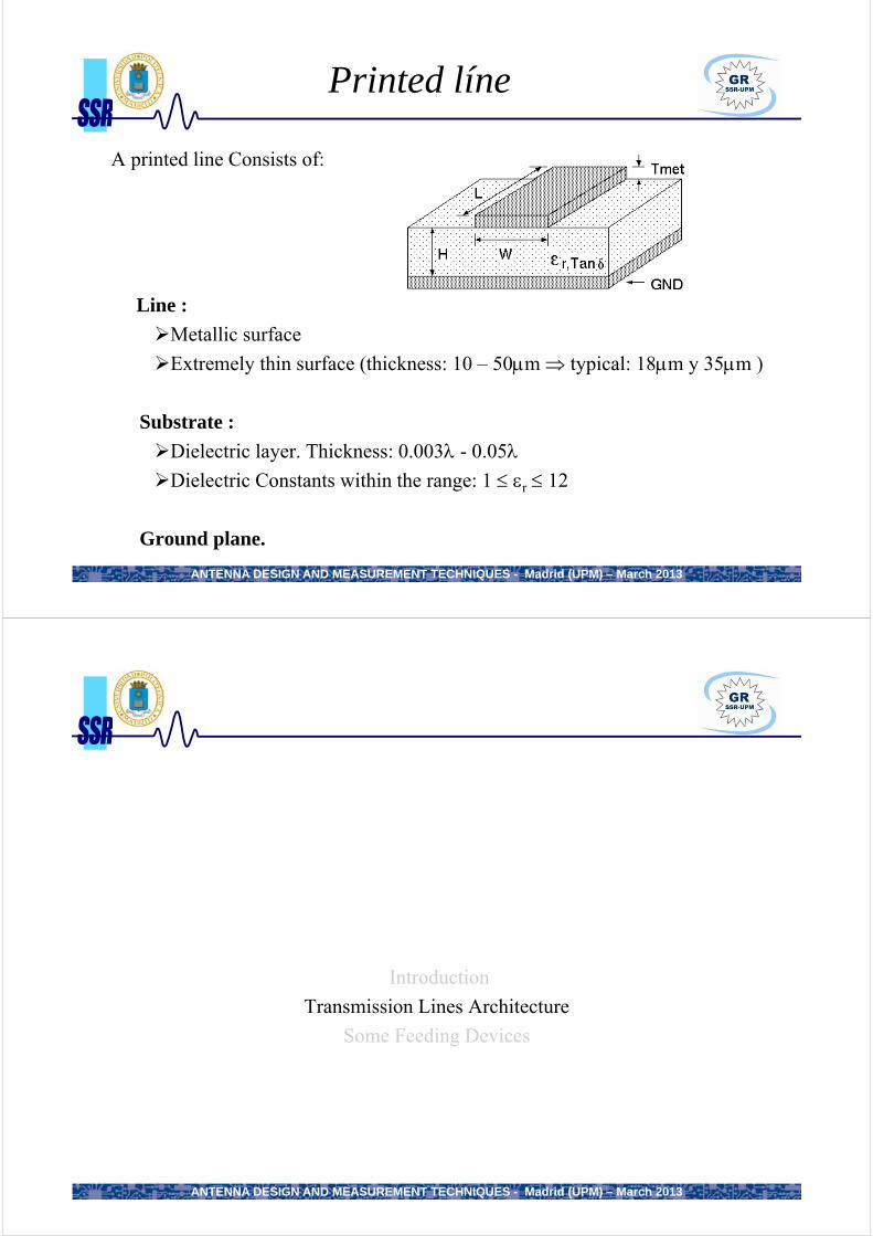
Printed líne
A printed line Consists of:
Line :
Metallic surface
Extremely thin surface (thickness: 10 – 50m typical: 18m y 35m )
Substrate :
Dielectric layer. Thickness: 0.003 - 0.05Dielectric Constants within the range: 1 r 12
Ground plane.
ANTENNA DESIGN AND MEASUREMENT TECHNIQUES - Madrid (UPM) – March 2013
Introduction
Transmission Lines Architecture
Some Feeding Devices
ANTENNA DESIGN AND MEASUREMENT TECHNIQUES - Madrid (UPM) – March 2013
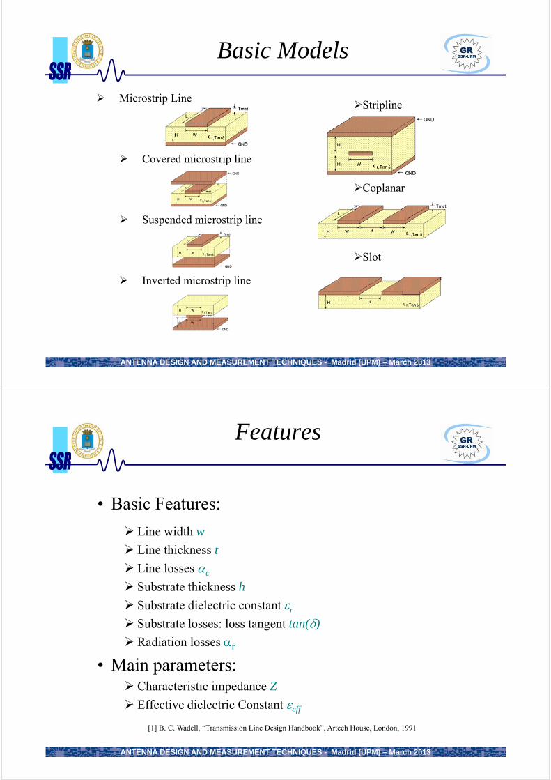
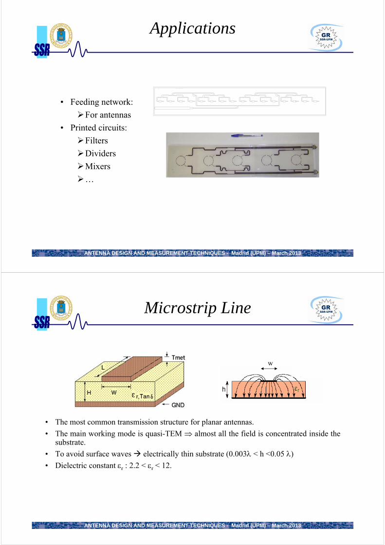
Microstrip Line
Covered microstrip line
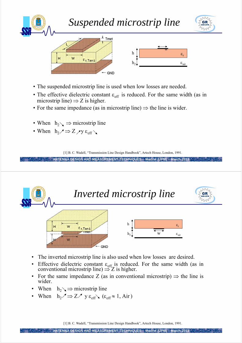
Suspended microstrip line
Inverted microstrip line
Basic Models
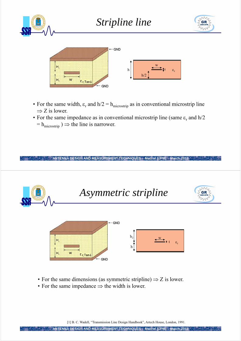
Stripline
Coplanar
Slot
ANTENNA DESIGN AND MEASUREMENT TECHNIQUES - Madrid (UPM) – March 2013
• Basic Features:
Line width w
Line thickness t
Line losses c
Substrate thickness h
Substrate dielectric constant r
Substrate losses: loss tangent tan()
Radiation losses r
• Main parameters: Characteristic impedance Z
Effective dielectric Constant eff
Features
[1] B. C. Wadell, “Transmission Line Design Handbook”, Artech House, London, 1991
ANTENNA DESIGN AND MEASUREMENT TECHNIQUES - Madrid (UPM) – March 2013
Layer Wavelength g :
Non-homogeneous dielectric:
Non-homogeneous dielectrics: when we have several dielectric layers (multilayer structure) or even when r, r change depending on the dielectric layer position.
The effective dielectric layer eff takes into account the wave propagation inside non-homogeneous dielectric layers.
Features
rr
g 0
eff
g 0
ANTENNA DESIGN AND MEASUREMENT TECHNIQUES - Madrid (UPM) – March 2013
Limitations
We have to Adopt a compromise solution
Layer thickness h
Reduce surface wave losses h
Increase bandwidth h
Substrate dielectric constant r
Tiny structures r
Line width w
w << g/2
Decrease undesired line radiation w << g/2
ANTENNA DESIGN AND MEASUREMENT TECHNIQUES - Madrid (UPM) – March 2013
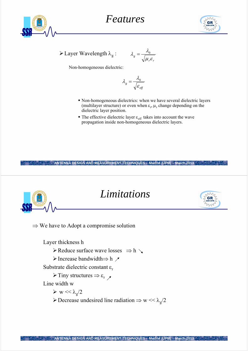
Applications
• Feeding network:
For antennas
• Printed circuits:
Filters
Dividers
Mixers
…
L16 S90-120ETSIT - S.R. MOYANO
ANTENNA DESIGN AND MEASUREMENT TECHNIQUES - Madrid (UPM) – March 2013
• The most common transmission structure for planar antennas.
• The main working mode is quasi-TEM almost all the field is concentrated inside thesubstrate.
• To avoid surface waves electrically thin substrate (0.003 < h <0.05 )
• Dielectric constant r : 2.2 < r < 12.
w
Microstrip Line
ANTENNA DESIGN AND MEASUREMENT TECHNIQUES - Madrid (UPM) – March 2013
Suspended microstrip line
• The suspended microstrip line is used when low losses are needed.
• The effective dielectric constant eff is reduced. For the same width (as inmicrostrip line) Z is higher.
• For the same impedance (as in microstrip line) the line is wider.
• When h2 microstrip line
• When h2 Z y eff
r
air
h
h2
w
[1] B. C. Wadell, “Transmission Line Design Handbook”, Artech House, London, 1991.
ANTENNA DESIGN AND MEASUREMENT TECHNIQUES - Madrid (UPM) – March 2013
Inverted microstrip line
• The inverted microstrip line is also used when low losses are desired.• Effective dielectric constant eff is reduced. For the same width (as in
conventional microstrip line) Z is higher.• For the same impedance Z (as in conventional microstrip) the line is
wider.• When h2 microstrip line• When h2 Z y eff (eff 1, Air )
r
air
h
h2 w
[1] B. C. Wadell, “Transmission Line Design Handbook”, Artech House, London, 1991.
ANTENNA DESIGN AND MEASUREMENT TECHNIQUES - Madrid (UPM) – March 2013
Stripline line
air
h r
w
h/2
t
• For the same width, r and h/2 = hmicrostrip as in conventional microstrip line Z is lower.
• For the same impedance as in conventional microstrip line (same r and h/2 = hmicrostrip ) the line is narrower.
ANTENNA DESIGN AND MEASUREMENT TECHNIQUES - Madrid (UPM) – March 2013
Asymmetric stripline
[1] B. C. Wadell, “Transmission Line Design Handbook”, Artech House, London, 1991.
h
air
r
h2 wt
• For the same dimensions (as symmetric stripline) Z is lower.• For the same impedance the width is lower.
ANTENNA DESIGN AND MEASUREMENT TECHNIQUES - Madrid (UPM) – March 2013
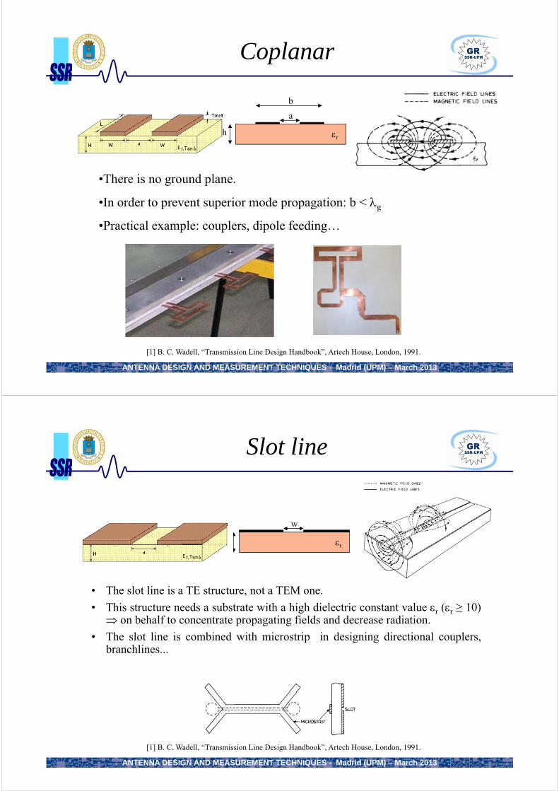
Coplanar
rh
a
b
[1] B. C. Wadell, “Transmission Line Design Handbook”, Artech House, London, 1991.
•There is no ground plane.
•In order to prevent superior mode propagation: b < g
•Practical example: couplers, dipole feeding…
ANTENNA DESIGN AND MEASUREMENT TECHNIQUES - Madrid (UPM) – March 2013
Slot line
• The slot line is a TE structure, not a TEM one.
• This structure needs a substrate with a high dielectric constant value r (r ≥ 10) on behalf to concentrate propagating fields and decrease radiation.
• The slot line is combined with microstrip in designing directional couplers,branchlines...
rh
w
[1] B. C. Wadell, “Transmission Line Design Handbook”, Artech House, London, 1991.
ANTENNA DESIGN AND MEASUREMENT TECHNIQUES - Madrid (UPM) – March 2013
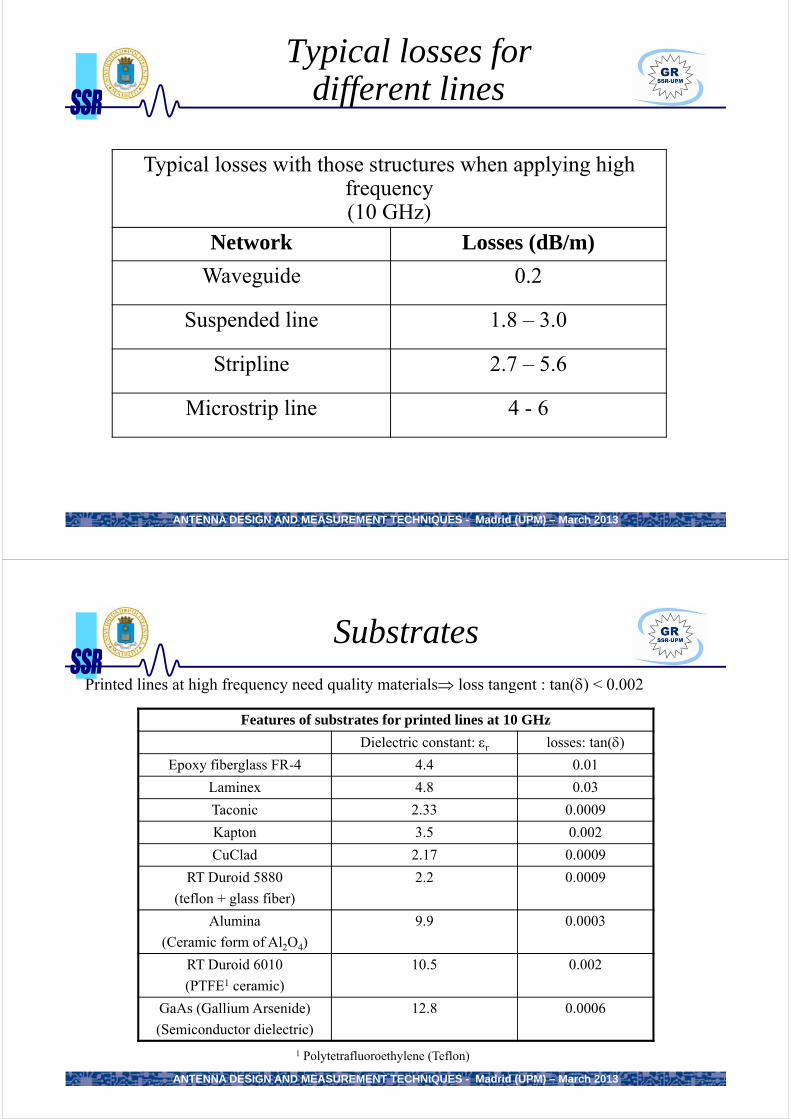
Typical losses for different lines
Typical losses with those structures when applying high frequency(10 GHz)
Network Losses (dB/m)
Waveguide 0.2
Suspended line 1.8 – 3.0
Stripline 2.7 – 5.6
Microstrip line 4 - 6
ANTENNA DESIGN AND MEASUREMENT TECHNIQUES - Madrid (UPM) – March 2013
SubstratesPrinted lines at high frequency need quality materials loss tangent : tan() < 0.002
Features of substrates for printed lines at 10 GHz
Dielectric constant: r losses: tan()
Epoxy fiberglass FR-4 4.4 0.01
Laminex 4.8 0.03
Taconic 2.33 0.0009
Kapton 3.5 0.002
CuClad 2.17 0.0009
RT Duroid 5880
(teflon + glass fiber)
2.2 0.0009
Alumina
(Ceramic form of Al2O4)
9.9 0.0003
RT Duroid 6010
(PTFE1 ceramic)
10.5 0.002
GaAs (Gallium Arsenide)
(Semiconductor dielectric)
12.8 0.0006
1 Polytetrafluoroethylene (Teflon)

ANTENNA DESIGN AND MEASUREMENT TECHNIQUES - Madrid (UPM) – March 2013
Substrate selection
Substrate thickness r
Reduction in line radiation Quite little high
Small dimensions little high
Low Losses little low
Reduction in losses due to surface currents little low
Increase in band width big low
Thin substrates with high r are used in microwave circuitry, as feeding network:
Advantages:Lower line width.Reduction in radiation and coupling effects, although they should not be neglected.
Disadvantaged:Higher losses.Lower efficiency. Lower bandwidth.
ANTENNA DESIGN AND MEASUREMENT TECHNIQUES - Madrid (UPM) – March 2013
Introduction
Transmission Lines Architecture
Some Feeding Devices
ANTENNA DESIGN AND MEASUREMENT TECHNIQUES - Madrid (UPM) – March 2013
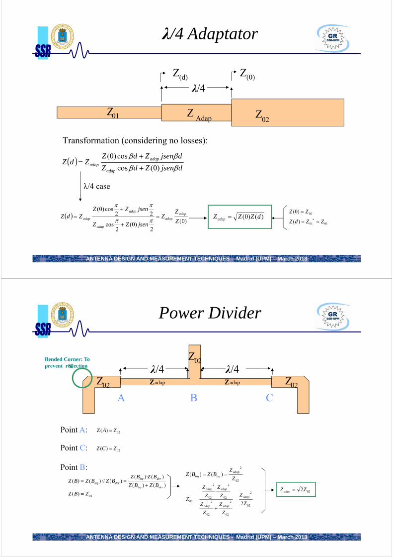
Transformation (considering no losses):
λ/4 Adaptator
λ/4
Z 02
Z 01 Z Adap
djsenZdZ
djsenZdZZdZ
adap
adapadap
)0(cos
cos)0(
λ/4 case
)0(
2)0(
2cos
22cos)0(
Z
ZZ
jsenZZ
jsenZZZdZ adap
adap
adap
adap
adap
)()0( dZZZ adap
Z (d) Z (0)
02)0( ZZ
0101)( ZZdZ
ANTENNA DESIGN AND MEASUREMENT TECHNIQUES - Madrid (UPM) – March 2013
Power Divider
02)( ZAZ
λ/4Z 02
λ/4Z 02
Z 02
Zadap Zadap
A B C
Point A:
02)( ZCZ Point C:
Point B:
02)( ZBZ
)()(
)()·()(//)()(
derizq
derizqderizq BZBZ
BZBZBZBZBZ
02
2
)()(Z
ZBZBZ adap
izqizq
02
2
02
2
02
202
2
02
2
02 2
·
Z
Z
Z
Z
Z
Z
Z
Z
Z
Z
Z adap
adapadap
adapadap
022ZZ adap
Bended Corner: To prevent reflection
ANTENNA DESIGN AND MEASUREMENT TECHNIQUES - Madrid (UPM) – March 2013
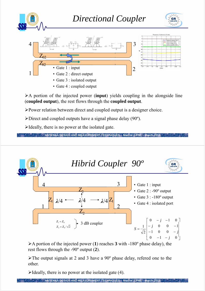
Directional Coupler
Z 02
Z 02
• Gate 1 : input
• Gate 2 : direct output
• Gate 3 : isolated output
• Gate 4 : coupled output
A portion of the injected power (input) yields coupling in the alongside line(coupled output), the rest flows through the coupled output.
Power relation between direct and coupled output is a designer choice.
Direct and coupled outputs have a signal phase delay (90º).
Ideally, there is no power at the isolated gate.
12
34
ANTENNA DESIGN AND MEASUREMENT TECHNIQUES - Madrid (UPM) – March 2013
Hibrid Coupler 90º
Z 2
Z 2• Gate 1 : input
• Gate 2 : -90º output
• Gate 3 : -180º output
• Gate 4 : isolated port
A portion of the injected power (1) reaches 3 with -180º phase delay), therest flows through the -90º output (2).
The output signals at 2 and 3 have a 90º phase delay, refered one to theother.
Ideally, there is no power at the isolated gate (4).
1 2
34
λ/4 λ/4Z Z 1 1λ/4
01 ZZ
2/02 ZZ 3 dB coupler
010
001
100
010
2
1
j
j
j
j
S

ANTENNA DESIGN AND MEASUREMENT TECHNIQUES - Madrid (UPM) – March 2013
Circular Coupler (Rat Race)
• Gate 1 : input
• Gate 2 : output -90º
• Gate 3 : isolated port
• Gate 4 : output -270º
The injected power at 1 reaches 2 and 4 with a phase delay of -/+90ºrespectively.
The output signals at 2 and 4 have a 180º phase delay, referred one tothe other.
Ideally, there is no power at the isolated gate (3).
1
2 3
4
00
00
00
00
2
1
jj
jj
jj
jj
S
λ/4
λ/4
λ/4
3λ/4
ANTENNA DESIGN AND MEASUREMENT TECHNIQUES - Madrid (UPM) – March 2013
References
[1] B. C. Wadell, “Transmission Line Design Handbook”, Ed. Artech House, London, 1991.
[2] E. Hammerstad, O.Jensen, “Accurate Models for Microstrip Computer-Aided Design”, IEEE MTT-S Symposium Digest, pp.407-409, June 1980.
[3] S. J. Orfanidis, “Electromagnetic Waves & Antennas”, 2004.
[4] H. Howe, “Stripline Circuit Design”, Ed. Artech House, London, 1982.
[5] D.M. Pozar, “Microwave Engineering”, Ed. John Wiley & Sons, 1980.
[6] K.C. Gupta, R. Garg, I. Bahl and P. Bhartia, “Microstrip Lines and Slotlines”, Artech House, London, 1996.
[7] P. Barthia & al., “Milimeter wave microstrip and printed circuit antennas”, Norwood, Mass, Ed. Artech House,1991.
[8] Ansoft Ensemble, “Ansoft Ensemble: Getting Started and Tutorials”, Versión 8.0 Copyright 1984-1999, Ansoft Coporation, 1999.