Embed Size (px)
Citation preview
Journal of ELECTRICAL ENGINEERING, VOL. 64, NO. 3, 2013, 143–151
FEEDBACK LOOP CONTROL STRATEGIESOF THE MULTI DC BUS LINK VOLTAGES
USING ADAPTIVE FUZZY LOGIC CONTROL
Farid Bouchafaa∗— Mohamed Seghir Boucherit
∗
— El Madjid Berkouk∗∗
Voltage source multilevel inverters have become very attractive for power industries in power electronics applicationsduring last years. The main purposes that have led to the development of the studies about multilevel inverters are thegeneration of output voltage signals with low harmonic distortion; the reduction of switching frequency. A serious constraintin a multilevel inverter is the capacitor voltage-balancing problem. The unbalance of different DC voltage sources of five-levelneutral point clamping (NPC) voltage source inverter (VSI) constitutes the major limitation for the use of this new powerconverter. In order to stabilize these DC voltages, we propose in this paper to study the cascade constituted by three phasesfive-level PWM rectifier, a clamping bridge and five-level NPC (VSI). In the first part, we present a topology of five-levelNPC VSI, and then they propose a model of this converter and an optimal PWM strategy to control it using four bipolarcarriers. Then in the second part, we study a five-level PWM rectifier, which is controlled by a multiband hysteresis strategy.In the last part of this paper, the authors study shows particularly the problem of the stability of the multi DC voltagesof the inverter and its consequence on the performances of the induction motors (IM). Then, we propose a solution to theproblem by employed closed loop regulation using PI regulator type fuzzy logic controller (FLC). The results obtained withthis solution confirm the good performances of the proposed solution, and promise to use the inverter in high voltage andgreat power applications as electrical traction.
K e y w o r d s: NPC inverter, clamping bridge, rectifier multilevel, PWM strategy, enslavement, fuzzy logic control
1 INTRODUCTION
Multilevel are based on the neutral point clamped(NPC) inverters topology and were proposed firstly byNabae and al [1]. Multilevel inverter structures provide anattractive solution for high power and high voltage appli-cations. While the multilevel topology lets higher voltagesusing devices of lower ratings, the link multi DC voltagebalancing problem is a serious drawback which limits theapplicability of multilevel topology for motor drives. Oneof the major limitations of the multilevel inverters is theinstability of the input multi DC voltages [2, 3].
In this work, the authors study a new AC/DC/ACconverter five-level NPC PWM rectifier. It synthesis thestaircase voltage wave form several levels of multi DCvoltages.
In the first part, the knowledge model of this inverteris developed and also the used optimal PWM strategywhich requires four bipolar carriers. After that, we clearlyshow up the stability problem of the four inputs DCvoltage sources by studying a five-level PWM currentrectifier-clamping bridge-five-level NPC VSI-IM cascade.In the last part of this paper, we study the stabilityproblem of the input multi DC VSI [4]. For this, wepropose a solution to this problem by using fuzzy logiccontroller (FLC) feedback loops to regulate the total DC
voltages by using Proportional-Integral regulator [5, 6].The results obtained with this solution shows that theproposed solution is very efficient to solve the instabilityproblem of this multilevel inverter.
2 FIVE–LEVEL NPC VSI MODELLING
A multilevel voltage source inverter is a converterstructure able to proving a line to ground voltage, at eacharm, with more than two different levels in the range of 0to Uc volts. The numbers of levels N corresponds to thedifferent potential levels that each arm is able to deliverat the output. With the emerging concept of multilevelvoltage source inverters, some technological limitationsof two-level standard inverter can be reduced or avoidedmaking possible the use to low cost semi conductors forhigh power applications drive. Also, lower harmonics dis-tortion and electromagnetic interferences is expected withthis new kind of static converter.
Different circuit topologies have been presented to im-plement this kind of converter, able of proving an outputvoltage with the mentioned characteristics. One of themost typical ones is the neutral point Clamped (NPC).
In this topology, a series connection of N−1 capacitorsis done to create N − 2 points with different potentials.
∗Laboratory of Instrumentation, Faculty of Electronics and Computer, University of Sciences and Technology Houari Boumediene,
BP 32 El-Alia 16111 Bab-Ezzouar Algeria, [email protected]∗∗
Laboratory of Process Control. Polytechnic National Institute Algiers,Street Hassen Badi, El Harrach, Algiers BP N◦ 182, [email protected], ms [email protected]
DOI: 10.2478/jee-2013-0021, ISSN 1335-3632 c© 2013 FEI STU
144 F. Bouchafaa — M.S. Boucherit — E.M. Berkouk: FEEDBACK LOOP CONTROL STRATEGIES OF THE MULTI DC BUS LINK . . .
Id1
Id3
Id0
S13
S17
S12
S11
D11
S14
S18
S15
S16
D10
S23
S27
S22
S21
D21
S24
S28
S25
S26
D20
S33
S37
S32
S31
D31
S34
S38
S35
S36
D30
IA IB IC
VAId4 VCVB
Uc4
Uc3
Uc2
Uc1
S33
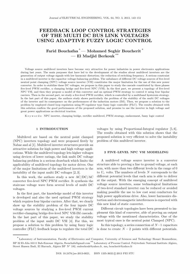
Fig. 1. A Five-level NPC voltage source inverter
Considering in a first approach, that the capacitors froman ideal voltage divider, each point is a DC potential andmay be connected to the output by switching on the con-venient electronics switches. This characteristic permitsthe generations of the N−2 intermediate voltage at eacharm output which Uc and zero voltages always available,constitute the total of N -level voltage generation mecha-nism. A generic N-level, NPC topology arm presents thefollowing characteristics [7]:
– Each output voltage levels is provided by only onecombination of the switches states, so even at steadystate operation some switches may have higher switch-ing frequency than others.
– Voltage across each opened electronics switch is intrin-sically limited to Uc/(N − 1).
– The number of capacitors needed of middle point gen-eration is N − 1. The number of clamping diodes is2(N − 2).
The general structure of the three phase’s five-levelNPC voltage source inverter is shown in Fig. 1. It isconstituted by three arms and four DC voltages sources.Every arm has eight bi-directional switches, six in seriesand two in parallel and two diodes Di0 and Di1 (i ∈{1, 2, 3}) which let to have zero voltage for VKM . VKM
is the voltage of the phase K relatively to the middlepoint M , where K ∈ {A,B,C} [7].
2.1 Knowledge model of the five-level NPC VSI
For this study we will consider that semiconductorsare ideal. If semiconductors are assumed in a controllablemode, we can define for each semi-conductor Tis a switch-ing function Sis corresponding switch state (1 =turned
on and 0 =turned off) [1, 3]: Several complementary lawsare possible for the five-level NPC VSI. The optimal oneis given below
Bi1 = Bi5 , Bi2 = Bi4 and Bi3 = Bi6 .
BiS is the control signal of the semiconductor TiS .(1)
The output voltage of the inverter, relatively to the mid-dle point M, is given by the following system
VKM = Si1Si2(1−Si3)UC1+Si1Si2Si3(1−Si4)(UC1+UC2)
− Si4Si5(1− Si6)UC3 − Si4Si5(1− Si6)(UC3 + UC4) .(2)
In order to get a simple model to design the control, wedefine equivalent switching functions Sb
i1 and Sbi0 and a
global half arm(
SbTi1 , SbT
i0 ) switching function associatedrespectively to the upper and lower half commutationcells.
Sbi1 = Si1Si2Si3 ,
Sbi0 = Si6Si7Si8 ,
SbTi1 = Si7 + Sb
i1 ,
SbTi0 = Si8 + Sb
i0 .
(3)
We suppose that capacitor voltages are balanced: Uc1 =Uc2 = Uc3 = Uc4 = Uc , the simple voltages of the threephases five-level NPC VSI are given by
VA
VB
VC
=1
3
2 −1 −1−1 2 −1−1 −1 2
S11bT − SbT10
S21bT − SbT20
S31bT − SbT30
UC . (4)
The input currents of the inverter are
id1 = S17i1 + S27i2 + S37i3 ,
id2 = Sb11i1 + Sb
21i2 + Sb31i3 ,
id3 = S18i1 + S28i2 + S38i3 ,
id4 = Sb10i1 + Sb
20i2 + Sb30i3
(5)
with
id0 = (i1 + i2 + i3)−(
SbT11 + SbT
10
)
i1 −(
SbT21 + SbT
20
)
i2
−(
SbT31 + SbT
30
)
i3 . (6)
2.2 Optimal PWM strategies method
Other authors have extended two-level carrier-basedPMWM techniques to multilevel inverters by making theuse of several triangular carrier signals and one referencesignal per phase. For N -level inverter, (N − 1) carrierswith the same frequency fc and same peak to peak am-plitude Ac are disposed such that the bands they occupyare contiguous. The reference, or modulation, wave formhas peak to peak amplitude Am and frequency fm , andit is centred in the middle of the carrier set. The reference
Journal of ELECTRICAL ENGINEERING 64, NO. 3, 2013 145
Fig. 2. A Five-level NPC voltage source inverterUc2
Vnet2
Vnet3
Inet3
Inet2
Uc1C1
irect2
irect1
irect3
i2
i1
i3
irect0
irect4
C2
C3
C4
Uc2
Uc3
Uc4
G
id2
id1
id3
id0
id4
Vnet1
Inet1R-L
Vnet2
Inet2R-L
Vnet3
Inet3R-L
IM
Five-level
PWM recifier
Five-level
NPC VSI
Fig. 3. Five level PWM rectifier-clamping bridge
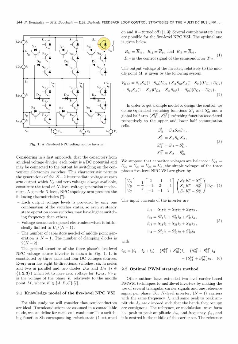
is continuously compared with each of the carrier signals.If the reference is greater than a carrier signal, then theactive device corresponding to that carrier is switched on;and if the reference is less than a carrier signal, then theactive corresponding to that carrier is switched off [2].
In multilevel inverters, the amplitude modulation in-dex, ma and the frequency ratio, mf are defined asma = Am/Ac = fc/fm .
The principle of this strategy optimal PWM witch issimilar to sub harmonic PWM except that a zero se-quence (triplen harmonic) voltage is added to each of thecarrier waveforms. This method takes the instantaneousaverage of the maximum and minimum of the three ref-erence voltages VSref = (V ∗
a , V∗
b , V∗
c ) and subtracts this
value from each of the individual reference voltages to ob-tain the modulation waveform [2, 3]. The voltage Voffset
is given by
Voffset =max(VSref) + min(VSref)
2. (7)
The new reference vectors are defined as follows
V ∗
Kref = V ∗
K − Voffset . (8)
Figure 2 represents the simple output voltage of the five-level NPC VSI controlled by the proposed optimal PWMstrategy with four bipolar carriers for m = 9, 12 andr = 0.9. We notice that, for even values of m , the simpleoutput voltage has symmetry relatively to the quarter ofthe period, and we have only odd harmonics. But for oddvalues of m , we have no symmetry, and then even andodd harmonics exist. The voltage harmonics gather byfamilies centred around frequencies multiple of 4mf .
3 FIVE–LEVEL PWM
RECTIFIER–CLAMPING BRIDGE–FILTER–
FIVE–LEVEL NPC VSI–CASCADE
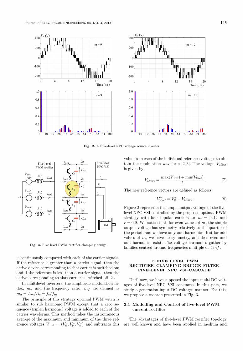
Until now, we have supposed the input multi DC volt-ages of five-level NPC VSI constants. In this part, westudy a generation input DC voltages manner. For this,we propose a cascade presented in Fig. 3.
3.1 Modelling and Control of five-level PWM
current rectifier
The advantages of five-level PWM rectifier topologyare well known and have been applied in medium and
146 F. Bouchafaa — M.S. Boucherit — E.M. Berkouk: FEEDBACK LOOP CONTROL STRATEGIES OF THE MULTI DC BUS LINK . . .
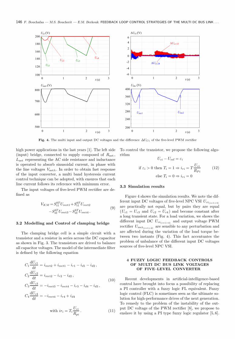
Fig. 4. The multi input and output DC voltages and the difference ∆UCi of the five-level PWM rectifier
high power applications in the last years [1]. The left side(input) bridge, connected to supply composed of Rnet ,Lnet representing the AC side resistance and inductanceis operated to absorb sinusoidal current, in phase withthe line voltages Vnetλ . In order to obtain fast responseof the input converter, a multi band hysteresis currentcontrol technique can be adopted, with ensures that eachline current follows its reference with minimum error.
The input voltages of five-level PWM rectifier are de-fined as
VKM =SbTi1 Urect1+SbT
i1 Urect2
−SbTi0 Urect3−SbT
i0 Urect4 .(9)
3.2 Modelling and Control of clamping bridge
The clamping bridge cell is a simple circuit with atransistor and a resistor in series across the DC capacitoras shown in Fig. 3. The transistors are drived to balanceall capacitor voltages. The model of the intermediate filteris defined by the following equation
C1
dUc1
dt= irect2 + irect1 − ir1 − id1 − id2 ,
C2
dUc2
dt= irect2 − ir2 − id2 ,
C3
dUc3
dt= −irect3 − irect4 − ir3 − id4 − id3 ,
C4
dUc4
dt= −irect4 − ir4 + id4
(10)
with iri = Ti
Uci
Rpi
. (11)
To control the transistor, we propose the following algo-rithm
Uci − Uref = εi
if εi > 0 then Ti = 1 ⇒ iri = TUci
RPi
else Ti = 0 ⇒ iri = 0
(12)
3.3 Simulation results
Figure 4 shows the simulation results. We note the dif-ferent input DC voltages of five-level NPC VSI Uci(i=1÷4)
are practically not equal, but by pairs they are equal(Uc1 = Uc3 and Uc2 = Uc4 ) and become constant aftera long transient state. For a load variation, we shows thedifferent input DC Uci(i=1÷4)
and output voltage PWM
rectifier Urect(i=1÷2)are sensible to any perturbation and
are affected during the variation of the load torque be-tween two instants (Fig. 4). This fact accentuates theproblem of unbalance of the different input DC voltagessources of five-level NPC VSI.
4 FUZZY LOGIC FEEDBACK CONTROLS
OF MULTI DC BUS LINK VOLTAGES
OF FIVE–LEVEL CONVERTER
Recent developments in artificial-intelligence-basedcontrol have brought into focus a possibility of replacinga PI controller with a fuzzy logic FL equivalent. Fuzzylogic control (FLC) is sometimes seen as the ultimate so-lution for high-performance drives of the next generation.To remedy to the problem of the instability of the out-put DC voltage of the PWM rectifier [8], we propose toenslave it by using a PI type fuzzy logic regulator [5, 6].
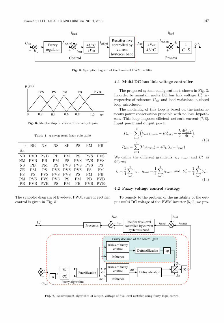
Journal of ELECTRICAL ENGINEERING 64, NO. 3, 2013 147
Fig. 5. Synoptic diagram of the five-level PWM rectifier
Fig. 6. Membership functions of the output gain
Table 1. A seven-term fuzzy rule table
e NB NM NS ZE PS PM PB
∆e
NB PVB PVB PB PM PS PVS PVSNM PVB PB PM PS PVS PVS PVSNS PB PM PS PVS PVS PVS PSZE PM PS PVS PVS PVS PS PMPS PS PVS PVS PVS PS PM PBPM PVS PVS PVS PS PM PB PVBPB PVB PVB PS PM PB PVB PVB
The synoptic diagram of five-level PWM current rectifiercontrol is given in Fig. 5.
4.1 Multi DC bus link voltage controller
The proposed system configuration is shown in Fig. 3.In order to maintain multi DC bus link voltage U ′
c , ir-respective of reference Uref and load variations, a closedloop introduced.
The modelling of this loop is based on the instanta-neous power conservation principle with no loss. hypoth-esis. This loop imposes efficient network current [7, 8].Input power and output power
Pin =
3∑
λ=1
(
Vnetλinetλ −Ri2netλ −L
2
di2netλ
dt
)
,
Pout =
4∑
i=1
(UCirecti) = 4UC(ic + iload) .
(13)
We define the different grandeurs ic , iload and U ′
c asfollows
ic =1
4
4∑
i=1
ici , iload =1
4
4∑
i=1
iloadi and U ′
c =1
4
4∑
i=1
U ′
c .
(14)
4.2 Fuzzy voltage control strategy
To remedy to the problem of the instability of the out-put multi DC voltage of the PWM inverter [5, 9], we pro-
Fig. 7. Enslavement algorithm of output voltage of five-level rectifier using fuzzy logic control
148 F. Bouchafaa — M.S. Boucherit — E.M. Berkouk: FEEDBACK LOOP CONTROL STRATEGIES OF THE MULTI DC BUS LINK . . .
t (s)0 1 2 3
DUci (V)
6
2
-2
-6
0
4
-4
DUci 13
DUci24
t (s)0 1 2 3
Uci (V)
200
180
160
140
120
100
Urect (V)
800
700
600
500
t (s)0 1 2 3
Urect (V)
400
360
320
280
240
200t (s)0 1 2 3
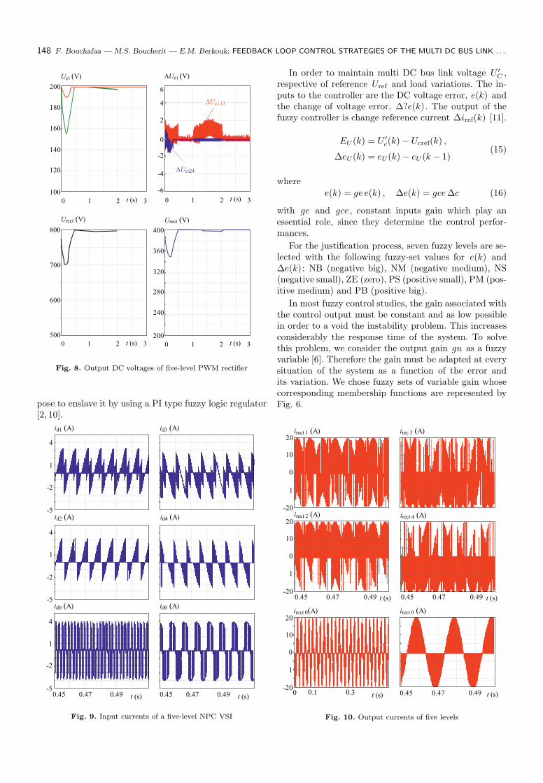
Fig. 8. Output DC voltages of five-level PWM rectifier
pose to enslave it by using a PI type fuzzy logic regulator[2, 10].
In order to maintain multi DC bus link voltage U ′
C ,respective of reference Uref and load variations. The in-puts to the controller are the DC voltage error, e(k) andthe change of voltage error, ∆?e(k). The output of thefuzzy controller is change reference current ∆iref(k) [11].
EU (k) = U ′
c(k)− Ucref(k) ,
∆eU (k) = eU (k)− eU (k − 1)(15)
where
e(k) = ge e(k) , ∆e(k) = gce∆c (16)
with ge and gce , constant inputs gain which play anessential role, since they determine the control perfor-mances.
For the justification process, seven fuzzy levels are se-lected with the following fuzzy-set values for e(k) and∆e(k): NB (negative big), NM (negative medium), NS(negative small), ZE (zero), PS (positive small), PM (pos-itive medium) and PB (positive big).
In most fuzzy control studies, the gain associated withthe control output must be constant and as low possiblein order to a void the instability problem. This increasesconsiderably the response time of the system. To solvethis problem, we consider the output gain gu as a fuzzyvariable [6]. Therefore the gain must be adapted at everysituation of the system as a function of the error andits variation. We chose fuzzy sets of variable gain whosecorresponding membership functions are represented byFig. 6.
4
1
-2
-5
id1 (A)
4
1
-2
-5
id0 (A)
t (s)0.45 0.47 0.49
4
1
-2
-5
id2 (A) id4 (A)
id3 (A)
id0 (A)
t (s)0.45 0.47 0.49
Fig. 9. Input currents of a five-level NPC VSI
irec 3 (A)
irect 0 (A)
t (s)0.45 0.47 0.49
irect 1 (A)20
10
0
-20
1
irect 2 (A)20
10
0
-20
1
t (s)0.45 0.47 0.49
irect 0(A)20
10
0
-20
1
t (s)0 0.1 0.3
irect 4 (A)
t (s)0.45 0.47 0.49
Fig. 10. Output currents of five levels
Journal of ELECTRICAL ENGINEERING 64, NO. 3, 2013 149
Fig. 11. The network current Inet and its voltage Vnet
The decision matrix on the control gain is given in
Table 1.
We use a regulator PI fuzzy logic for enslave multi
DC bus link voltage. The general principle enslavement of
five-level rectifier is given by Fig. 7. We use the algorithm
enslavement elaborate previously (Fig. 5) to control the
rectifier of the cascade we apply load variation between
two instants t = 1 s and t = 2 s.
Figures 8–11 show the simulation results when we use
a full clamping bridge and feedback control with PI fuzzy
logic regulator. We show the performances of the FLC of
the output voltage of the five-level PWM rectifier (Fig. 8).
We note that, the output voltage of PWM rectifier follows
perfectly its reference which is constant and are no effect
for the load variation (Fig. 8).
Therefore the different input DC voltages of the five-
level NPC VSI are constant and practically equal by pairs
too (Uc1 = Uc3 and Uc2 = Uc4 ), become constant after a
transient state and insensible to any perturbation (fig.8).
In consequence the output voltage of the five-level NPC
VSI is symmetrical.
The currents id1 and id2 are respectively the opposite
of the currents id3 and id4 respectively. The inverter
current rectifier id0 has a mean value nearly null (Fig. 9).
The currents rectifier irect1 and irect2 are the oppo-
site of the currents irect3 and irect4 , respectively. The
current irect0 has a mean value nearly null (Fig. 10). We
remark that the grid currents ineti feeding rectifier follow
their sinusoidal references (Fig. 11). The grid voltages and
currents are in phase then the power factor at the grid
connection is unit (Fig.11).
5 APPLICATION OF FEEDBACK
CONTROLALGORITHM OF
RECTIFIER OF THE CASCADE
In this part, we will study the performances of the
speed control of the induction motors fed by five-level
NPC inverter controlled by the proposed optimal PWM
strategies (Fig. 12).
In order to simulate the dynamics of the induction
motor, a simplified model has been developed. If all stator
and rotor variables are expressed in a rotating reference
frame and it is supposed that the 0 component is removed
for symmetry reason, the four equations for electrical
variables and the two mechanical equations are
Fig. 12. The speed control using fuzzy logic regulator
150 F. Bouchafaa — M.S. Boucherit — E.M. Berkouk: FEEDBACK LOOP CONTROL STRATEGIES OF THE MULTI DC BUS LINK . . .
Wr (rd/s)100
80
0
20
40
60
Te (Nm)
30
20
10
-10
0
40
Fdr
0
1.8
1.4
0.4
0.8
1.2
t (s)0 21 3
10
-10
0
ias(A)
t (s)0 21 3
Va(V)
400
-200
0
200
-420
ias (A)
t (s)0.35 0.45
0
-2
-4
4
2
Vs (V)
t (s)0.35 0.45
100
-100
300
0
-300
0.8
0.4
-0.4
0
Fqr
t (s)0 21 3
zoom
zoom
Fig. 13. Performances fed by five-level PWM rectifier-five-level NPC inverter-induction motors cascade
Vds = Rsids +d
dtΦds − ωsΦqs ,
Vqs = Rsiqs +d
dtΦqs − ωsΦds ,
Vdr = Rridr +d
dtΦdr ,
Vqr = Rriqr +d
dtΦqr ,
Te =3
2P(
iqsΦds − idsΦqs
)
.
(17)
Figure 13 shows the electromagnetic torque in studystate. The driver of the IM fed quietly its reference. Theoutput voltage of the five-level NPC VSI is sinusoidal andsymmetrical. To confirm the effectiveness of the proposedcontrol, a step load torque has been applied between 1 sand 2 s. Figure 13 shows that the line current is approx-
imately sinusoidal. The rapid change of the line currentshows that the system has a very good dynamic responseto load variation. After starting phase and the variationtest of the load torque, the machine stator current savethe sinusoidal form.
6 CONCLUSION
In this paper, the fuzzy adaptive controller is used tominimize harmonics of side network introduced by themultilevel converter, including the control of power fac-tor and we have studied the stability problem of the multiDC bus link voltage of the five-level NPC VSI using a cas-cade constituted by a five-level PWM rectifier-clampingbridge-five-level NPC VSI. We have particularly shown
the problem of the middle point of multi DC voltages
Journal of ELECTRICAL ENGINEERING 64, NO. 3, 2013 151
source supplied the five- level VSI and its effects the se-
rious problems of the speed control of induction motors
and the output voltages source of the five-level inverter is
asymmetric. To solve this problem, we propose the fuzzy
logic feedback control of the input voltages of the five-
level.
The use of the fuzzy logic feedback control has shown a
good tracking of AC grid current and the stability of multi
DC bus link voltages of the five-level NPC inverter. The
results obtained shows that the proposed solution is very
efficient to solve the instability problem of the multilevel
inverter. Several tests have been performed in order to
prove the efficiency of the type of the control. Simulation
results confirm the validity of this control technique. So,
now is possible to conceiver with frequency charger using
in output the five-level inverter, IM variator with feeble
rate of harmonics, a power factor of network unity and
great charge dynamics performance.
References
[1] NABAE, A. et al : A New Neutral Point Clamped PWM In-
verter, IEEE transaction on Industry Applications IA-17 No. 5
(Sep/Oct 1981), 518–523.
[2] HUR, N.—JUNG, J.—NAM, K. : A Fast Dynamic DC-Link
Power-Balance Scheme for a PWM Converter-Inverter System,
IEEE Tansactions on industrial electronics No. 4 (Aug 2001).
[3] OGASAWARA, S.—AKAGI, H. : A Vector control system us-
ing a neutral-point-clamped voltage source PWM inverter, IEEE
Transactions on Industry Applications (1991), 422-427.
[4] RODRGUEZ, J.et al : Modelling and Analysis of Common-
Mode Voltages Generated in Medium Voltage PWM-CSI Drives,
IEEE Transactions on Power Electronics 18 No. 3 (May 2003),
873–880.
[5] ZADEH, L. A. : Fuzzy Sets, Inform. Contr. 8 (1965), 338–353.
[6] KING, P. J.—MAMDANI, E. H. : The Application Fuzzy Algo-
rithms for Control Systems to Industrial Processes, Automatica
9 (1977), 235–242.
[7] CHIBANI, R.et al : Five-Level PWM Current Rectifier-Five-
Level NPC VSI-Permanent Magnet Synchronous Machine Cas-
cadejour The European Physical Journal Applied Physics.
[8] ISHIDA, T.—MATSUSE, K. : DC Voltage Control Strategy fora Five-Level Converter, IEEE Transactions on Power Electronics15 No. 3 (May 2000), 508–515.
[9] RODRIGUEZ. J.et al : Calculation of the DC-Bus Capacitors ofthe Back-to-Back NPC Converters, EPE-EPE-PEMC, Portoroz,Slovenia, 2006, pp. 137–142.
[10] MAZUMDER, S. K. : A Novel Discrete Control Strategyfor Independent Stabilization of Parallel Three-Phase BoostConverters by Combining Space-Vector Modulation with Vari-able-Structure Control, IEEE Trans. on Power Electronics 18
No. 4 (July 2003), 1070–1084.
[11] GAUBERT, J. P.et al : Design and Implementation of HighPerformance Direct Power Control of Three-Phase PWM Recti-fier via Fuzzy and PI Controller for Output Voltage Regulation,
ELSEVIER Energy Conversion and Management 50 (2009),6–13.
Received 22 August 2011
Farid Bouchafaa was born in Algiers, Algeria. In 1990received the BSc degree and the Magister degree in 1997 ininstrumentation and engineering systems from University ofScience and Technology Houari Boumediene, Algiers, Algeria.I obtained in 2006 the doctorate degree in electrical engineer-ing, from the National Polytechnic Institute, Algiers, Alge-ria. In 1999, he joined the Electrical Engineering Departmentof USTHB. He is member in Solar and modeling laboratory.His current research interests are in the area of control powerelectronics and process, electrical drives and energy renewable(Solar, Wind).
El Madjid Berkouk was born in 1968 in Algiers. He re-ceived the Engineer degree in Electrotechnics, in electrical en-gineering, from the Polytechnic National Institute, Algiers,Algeria, in 1992, and the PhD degree in power system fromCNAM, Paris, France in 1995. He is currently with the de-partment of Automatic control and Electrical Engineering ofPolytechnic National Institute. He is a Professor, member ofProcess Control Laboratory and his research interests are inthe area of electrical drives, process control and power system.
Mohamed Seghir Boucherit was born in 1954 in Al-giers. He received the Engineer degree in Electrotechnics, theMagister degree and the PhD degree in electrical engineer-ing, from the Polytechnic National Institute, Algiers, Alge-ria, in 1980, 1988 and 1995 respectively. Upon graduation, hejoined the Electrical Engineering Department of PolytechnicNational Institute. He is a Professor, member of Process Con-trol Laboratory and his research interests are in the area ofelectrical drives and process control.


![COMPARISONOFHONEYBEEMATINGOPTIMIZATION …iris.elf.stuba.sk/JEEEC/data/pdf/3_113-01.pdf · 2013. 5. 22. · system stability enhancement through improved damping of power swings [12]](https://img.pdfslide.us/doc/110x75/603e07791beee513e52b6291/comparisonofhoneybeematingoptimization-iriselfstubaskjeeecdatapdf3113-01pdf.jpg)


![Research Article Modeling and Analysis of the Weld …downloads.hindawi.com/journals/mpe/2013/473495.pdffeedback control of the welding process parameters [ ]. Murugan and Gunaraj](https://img.pdfslide.us/doc/110x75/5ebdbb30aaf1bc6c831deac9/research-article-modeling-and-analysis-of-the-weld-feedback-control-of-the-welding.jpg)