Embed Size (px)
Citation preview

© 2005 Fairchild Semiconductor Page 1
of 16 Rev 1.1 February 2005
www.fairchildsemi.com
FEB100-001 User’s Guide
5V/1A Flyback Converter For Auxiliary Power and Charging Applications
Featured FSC Products: FSDM311, FOD2741B
www.fairchildsemi.com/FEBsupport
© 2005 Fairchild Semiconductor Page 2
of 16 Rev 1.1 February 2005
www.fairchildsemi.com
Contents
1.
General Board Description .......................................................................................................................3
1.1
The contents of the FSDM311 Evaluation Kit .......................................................................................3
1.2
Power Supply Specification Table ......................................................................................................3
2.
Circuit Description...................................................................................................................................3
2.1
Auxiliary Supply Implementation........................................................................................................4
2.2
Lithium-Ion Charger Implementation....................................................................................................5
3.
Evaluation Board Connection....................................................................................................................6
4.
Test Procedure.........................................................................................................................................6
5.
Test Results .............................................................................................................................................7
5.1
Start-up ..........................................................................................................................................7
5.2
Operation.......................................................................................................................................8
6.
Parts List...............................................................................................................................................11
7.
Printed Circuit Board .............................................................................................................................12
8.
Featured Products..................................................................................................................................13
8.1
FSDM311 Controller Details ...........................................................................................................13
8.1.1
Description .........................................................................................................................13
8.1.2
Main Features of the FSDM311.............................................................................................13
8.1.3
FSDM311 Functional Block Diagram......................................................................................14
8.2
FOD2741 Details ..........................................................................................................................14
8.2.1
Description .........................................................................................................................14
8.2.2
Features .............................................................................................................................14
9.
References/Resources............................................................................................................................15
9.1
Application Notes ..........................................................................................................................15

© 2005 Fairchild Semiconductor Page 3
of 16 Rev 1.1 February 2005
www.fairchildsemi.com
1. General Board Description
The FEB100-001 Evaluation Board is a 5V/1A Flyback converter for auxiliary power and Lithium-Ion battery charging power supplies. The design uses the FSDM311 Fairchild Power Switch technology. It operates over a universal input range of 85 Vac to 265 Vac.
1.1 The Contents of the FEB100-001 Evaluation Kit
• FEB100-001 evaluation board• FEB100-001 evaluation board user’s guide• CD ROM containing the following:
– FEB100-001 User’s Guide– FSDM311 Data Sheet– FOD2741 Data Sheet– 2N3904 Data Sheet– IN4148 Data Sheet– SB360 Data Sheet– UF4007 Data Sheet– AN-4137 Design Guidelines for Off-line Flyback Converters Using FPS– AN-4138 Design Considerations for Battery Charger Using Green Mode FPS– AN-4141 Troubleshooting and Design Tips for FPS Flyback Applicatons– AN-4145 Electromagnetic Compatibility for Power Converters
1.2 Power Supply Specification Table
• 74% efficiency
Table 1. Power supply specifications.
2. Circuit Description
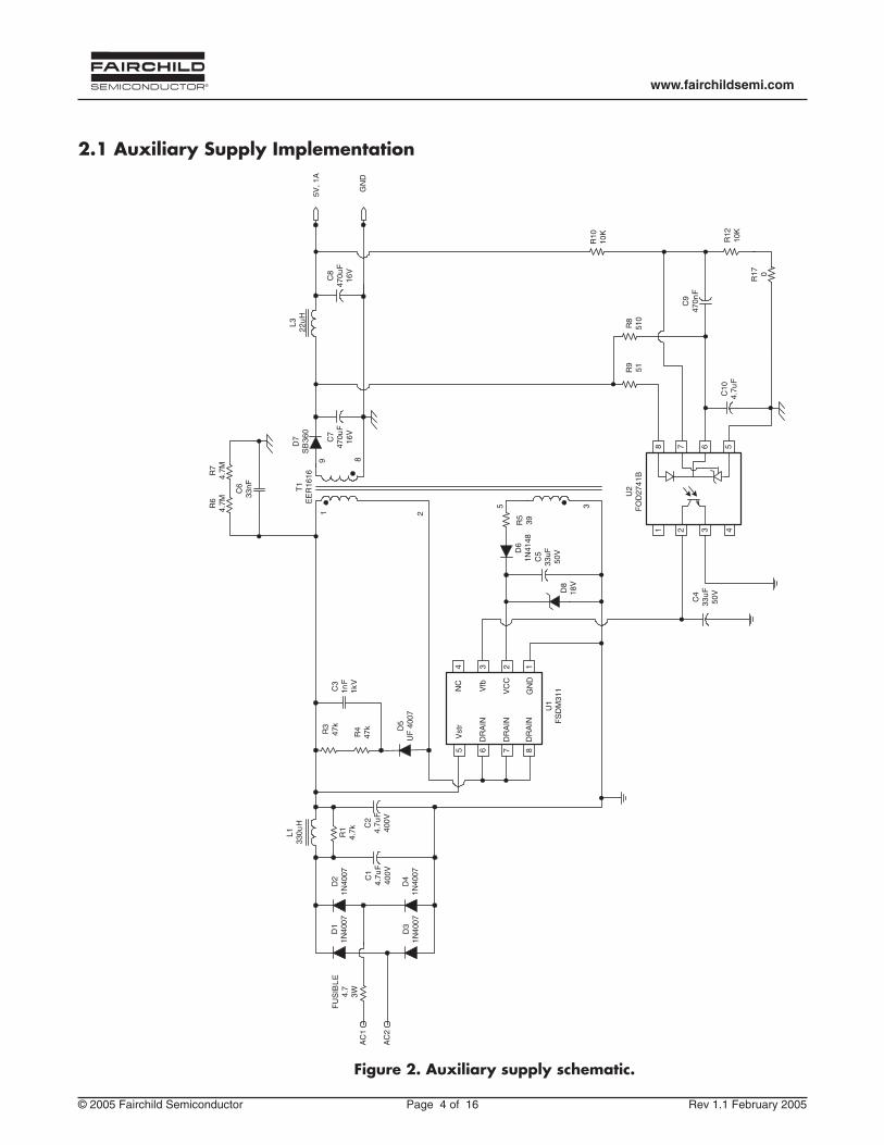
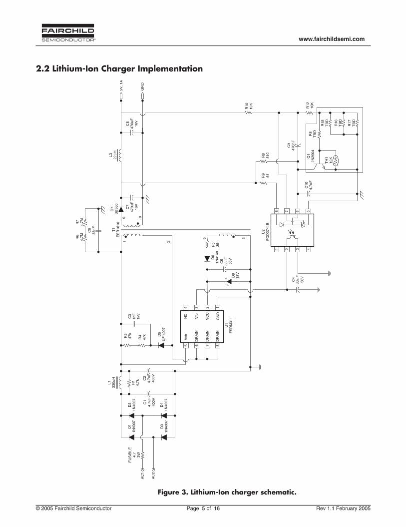
This circuit demonstrates the ability of the FSDM311 in an auxiliary or charging application. The circuit is shipped standard as an auxiliary power supply producing 5V at 1A. The secondary side can be changed by the addition of Q1, TH1, R15, R16, R17, & R19 to operate as a Lithium-Ion battery charger. A detailed design procedure including calculations can be found in AN-4138.
Figure 1. Photograph of evaluation board.
Voltage (V) VoltageRipple
Current (A)
Min Typ Max Min Typ Max
Output 1
4.95 5.0 5.05 120mV – 1 1.2
© 2005 Fairchild Semiconductor Page 4
of 16 Rev 1.1 February 2005
www.fairchildsemi.com
2.1 Auxiliary Supply Implementation
Figure 2. Auxiliary supply schematic.
T1
EE
R16
16
89
D7
SB
360
C7
470u
F16
V
C8
470u
F16
V
L322
uH
5V, 1
A
C3
1nF
1kV
1 2
5 3
C1
4.7u
F40
0V
R3
47k
R4
47k
L133
0uH
D5
UF
400
7
D1
1N40
07
D4
1N40
07D
31N
4007
D2
1N40
07F
US
IBL
E4.
73W
C2
4.7u
F40
0V
R1
4.7k
C5
33uF
50VD
61N
4148
R5
39
GN
D
8765
1234
GN
D
VC
C
Vfb
NC
DR
AIN
DR
AIN
DR
AIN
Vst
r
8 7 6 5
1 2 3 4
C4
33u
F50
VD8
18V
R6
4.7M
R7
4.7M
C6
33nF
U1
FS
DM
311
C10
4.7u
F
R9
51R
851
0
R12
10K
R10
10K
C9
470
nF
R17 0
U2
FO
D27
41B
AC
1
AC
2
© 2005 Fairchild Semiconductor Page 5
of 16 Rev 1.1 February 2005
www.fairchildsemi.com
2.2 Lithium-Ion Charger Implementation
Figure 3. Lithium-Ion charger schematic.
T1
EE
R16
16
89
D7
SB
360
C7
470u
F16
V
C8
470u
F16
V
L322
uH
5V, 1
A
C3
1nF
1kV
1 2
5 3
C1
4.7u
F40
0V
R3
47k
R4
47k
L133
0uH
D5
UF
400
7
D1
1N40
07
D4
1N40
07D
31N
4007
D2
1N40
07F
US
IBL
E4.
73W
C2
4.7u
F40
0V
R1
4.7k
C5
33uF
50VD
61N
4148
R5
39
GN
D
8765
1234
GN
D
VC
C
Vfb
NC
DR
AIN
DR
AIN
DR
AIN
Vst
r
8 7 6 5
1 2 3 4
C4
33u
F50
VD8
18V
R6
4.7M
R7
4.7M
C6
33n
F
U1
FS
DM
311
C10
4.7u
F
R9
51R
851
0
Q1
2N39
04R
8T
BD
R12
10K
R10
10K
C9
470
nF
R17
TB
D
R16
TB
D
R15
TB
DT
H1
10K
U2
FO
D27
41B
AC
1
AC
2
© 2005 Fairchild Semiconductor Page 6
of 16 Rev 1.1 February 2005
www.fairchildsemi.com
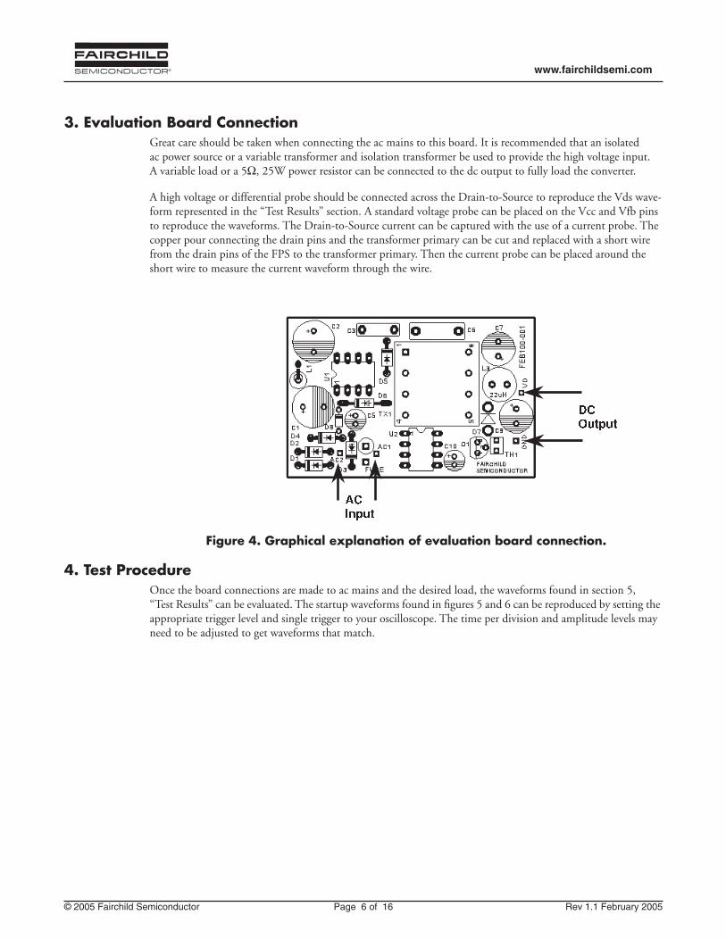
3. Evaluation Board Connection
Great care should be taken when connecting the ac mains to this board. It is recommended that an isolated ac power source or a variable transformer and isolation transformer be used to provide the high voltage input. A variable load or a 5
Ω
, 25W power resistor can be connected to the dc output to fully load the converter.
A high voltage or differential probe should be connected across the Drain-to-Source to reproduce the Vds wave-form represented in the “Test Results” section. A standard voltage probe can be placed on the Vcc and Vfb pins to reproduce the waveforms. The Drain-to-Source current can be captured with the use of a current probe. The copper pour connecting the drain pins and the transformer primary can be cut and replaced with a short wire from the drain pins of the FPS to the transformer primary. Then the current probe can be placed around the short wire to measure the current waveform through the wire.
Figure 4. Graphical explanation of evaluation board connection.
4. Test Procedure
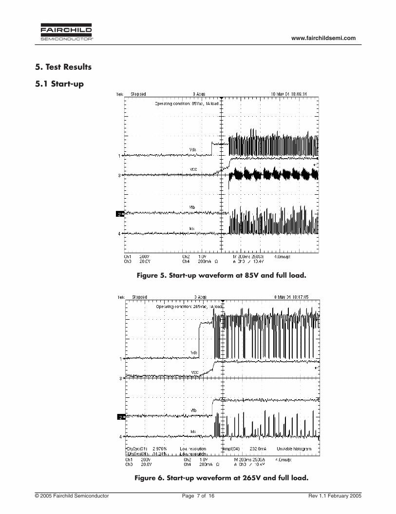
Once the board connections are made to ac mains and the desired load, the waveforms found in section 5, “Test Results” can be evaluated. The startup waveforms found in figures 5 and 6 can be reproduced by setting the appropriate trigger level and single trigger to your oscilloscope. The time per division and amplitude levels may need to be adjusted to get waveforms that match.
ACInput
DC Output
© 2005 Fairchild Semiconductor Page 7
of 16 Rev 1.1 February 2005
www.fairchildsemi.com
5. Test Results
5.1 Start-up
Figure 5. Start-up waveform at 85V and full load.
Figure 6. Start-up waveform at 265V and full load.
© 2005 Fairchild Semiconductor Page 8
of 16 Rev 1.1 February 2005
www.fairchildsemi.com
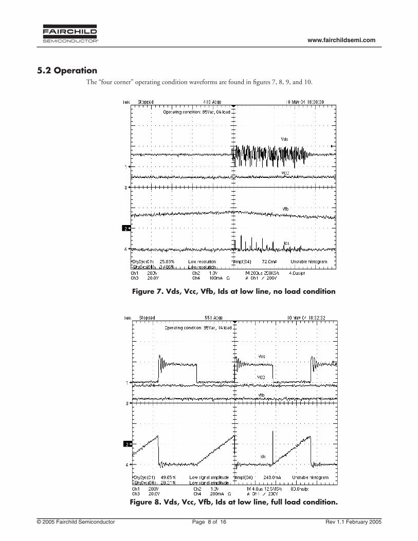
5.2 Operation
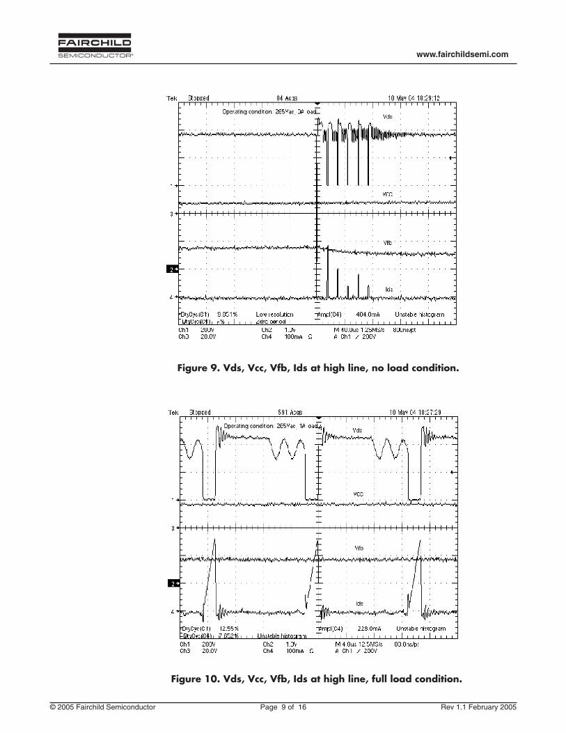
The “four corner” operating condition waveforms are found in figures 7, 8, 9, and 10.
Figure 7. Vds, Vcc, Vfb, Ids at low line, no load condition
Figure 8. Vds, Vcc, Vfb, Ids at low line, full load condition.
© 2005 Fairchild Semiconductor Page 9
of 16 Rev 1.1 February 2005
www.fairchildsemi.com
Figure 9. Vds, Vcc, Vfb, Ids at high line, no load condition.
Figure 10. Vds, Vcc, Vfb, Ids at high line, full load condition.
© 2005 Fairchild Semiconductor Page 10
of 16 Rev 1.1 February 2005
www.fairchildsemi.com
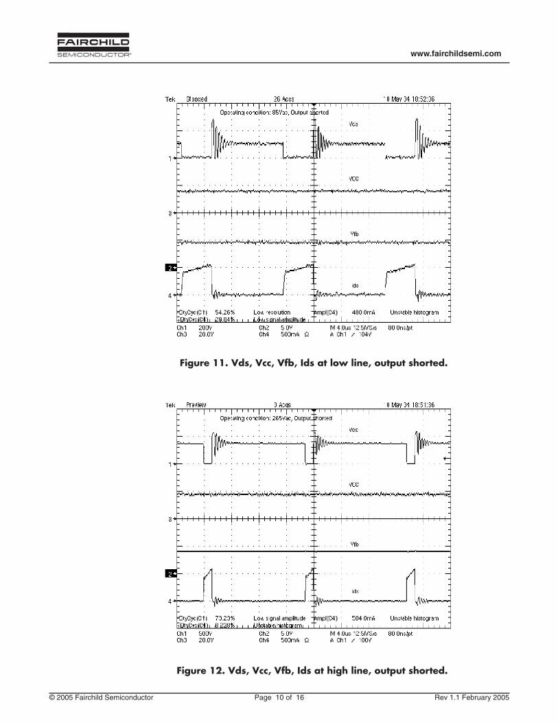
Figure 11. Vds, Vcc, Vfb, Ids at low line, output shorted.
Figure 12. Vds, Vcc, Vfb, Ids at high line, output shorted.
© 2005 Fairchild Semiconductor Page 11
of 16 Rev 1.1 February 2005
www.fairchildsemi.com
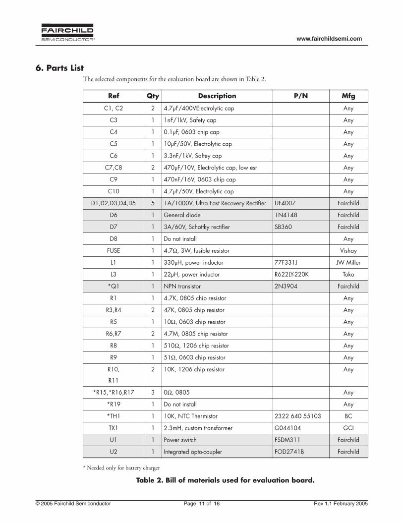
6. Parts List
The selected components for the evaluation board are shown in Table 2.
* Needed only for battery charger
Table 2. Bill of materials used for evaluation board.
Ref Qty Description P/N Mfg
C1, C2 2 4.7µF/400VElectrolytic cap Any
C3 1 1nF/1kV, Safety cap Any
C4 1 0.1µF, 0603 chip cap Any
C5 1 10µF/50V, Electrolytic cap Any
C6 1 3.3nF/1kV, Saftey cap Any
C7,C8 2 470µF/10V, Electrolytic cap, low esr Any
C9 1 470nF/16V, 0603 chip cap Any
C10 1 4.7µF/50V, Electrolytic cap Any
D1,D2,D3,D4,D5 5 1A/1000V, Ultra Fast Recovery Rectifier UF4007 Fairchild
D6 1 General diode 1N4148 Fairchild
D7 1 3A/60V, Schottky rectifier SB360 Fairchild
D8 1 Do not install Any
FUSE 1 4.7
Ω
, 3W, fusible resistor Vishay
L1 1 330µH, power inductor 77F331J JW Miller
L3 1 22µH, power inductor R622LY-220K Toko
*Q1 1 NPN transistor 2N3904 Fairchild
R1 1 4.7K, 0805 chip resistor Any
R3,R4 2 47K, 0805 chip resistor Any
R5 1 10
Ω
, 0603 chip resistor Any
R6,R7 2 4.7M, 0805 chip resistor Any
R8 1 510
Ω
, 1206 chip resistor Any
R9 1 51
Ω
, 0603 chip resistor Any
R10,
R11
2 10K, 1206 chip resistor Any
*R15,*R16,R17 3 0
Ω
, 0805 Any
*R19 1 Do not install Any
*TH1 1 10K, NTC Thermistor 2322 640 55103 BC
TX1 1 2.3mH, custom transformer G044104 GCI
U1 1 Power switch FSDM311 Fairchild
U2 1 Integrated opto-coupler FOD2741B Fairchild
© 2005 Fairchild Semiconductor Page 12
of 16 Rev 1.1 February 2005
www.fairchildsemi.com
Figure 13. Transformer specification.
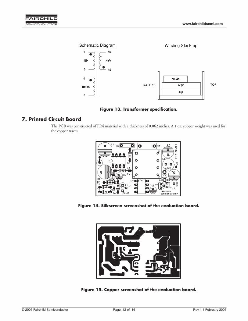
7. Printed Circuit Board
The PCB was constructed of FR4 material with a thickness of 0.062 inches. A 1 oz. copper weight was used for the copper traces.
Figure 14. Silkscreen screenshot of the evaluation board.
Figure 15. Copper screenshot of the evaluation board.
Nbias
1
3
4
8
15
16
Np
N5V
N5VNP
NbiasTOP
Schematic Diagram Winding Stack-up
BOTTOM
© 2005 Fairchild Semiconductor Page 13
of 16 Rev 1.1 February 2005
www.fairchildsemi.com
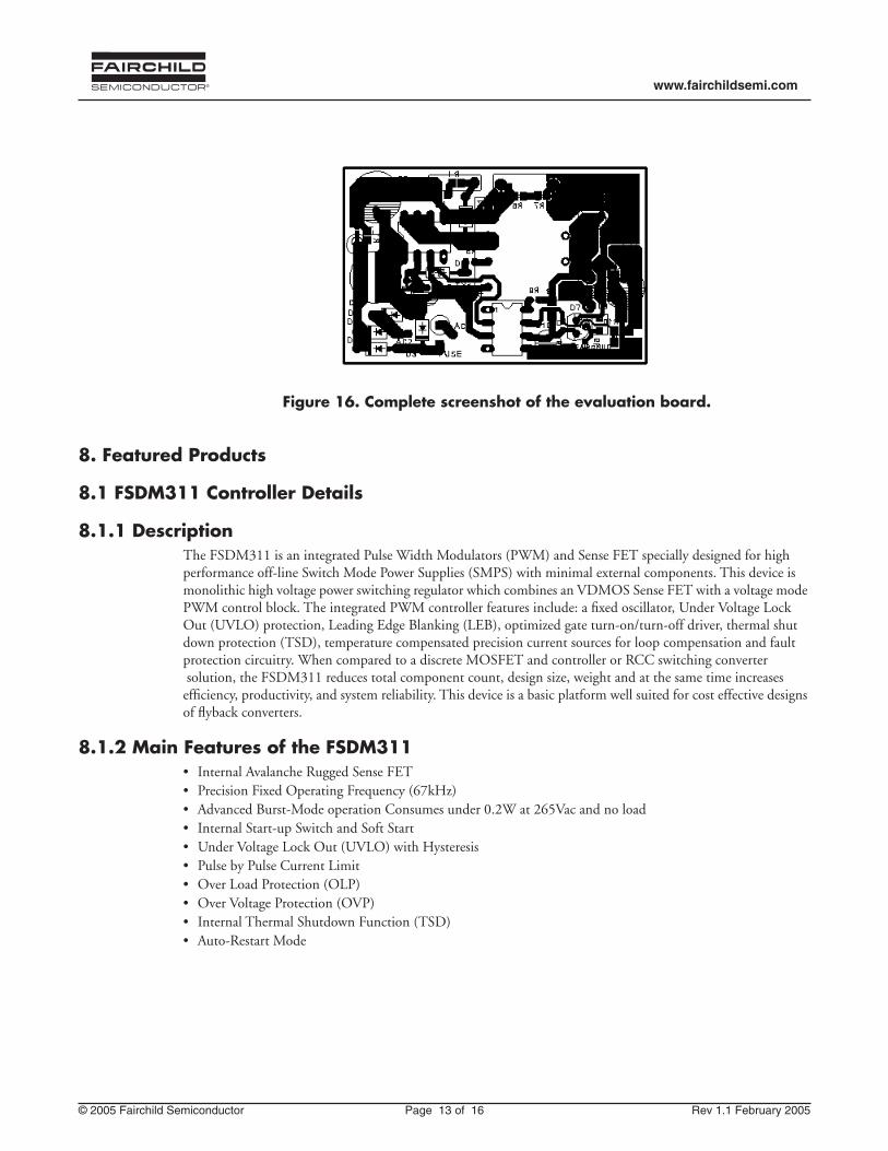
Figure 16. Complete screenshot of the evaluation board.
8. Featured Products
8.1 FSDM311 Controller Details
8.1.1 Description
The FSDM311 is an integrated Pulse Width Modulators (PWM) and Sense FET specially designed for high performance off-line Switch Mode Power Supplies (SMPS) with minimal external components. This device is monolithic high voltage power switching regulator which combines an VDMOS Sense FET with a voltage mode PWM control block. The integrated PWM controller features include: a fixed oscillator, Under Voltage Lock Out (UVLO) protection, Leading Edge Blanking (LEB), optimized gate turn-on/turn-off driver, thermal shut down protection (TSD), temperature compensated precision current sources for loop compensation and fault protection circuitry. When compared to a discrete MOSFET and controller or RCC switching converter solution, the FSDM311 reduces total component count, design size, weight and at the same time increases efficiency, productivity, and system reliability. This device is a basic platform well suited for cost effective designs of flyback converters.
8.1.2 Main Features of the FSDM311
• Internal Avalanche Rugged Sense FET • Precision Fixed Operating Frequency (67kHz) • Advanced Burst-Mode operation Consumes under 0.2W at 265Vac and no load • Internal Start-up Switch and Soft Start • Under Voltage Lock Out (UVLO) with Hysteresis • Pulse by Pulse Current Limit • Over Load Protection (OLP) • Over Voltage Protection (OVP) • Internal Thermal Shutdown Function (TSD) • Auto-Restart Mode
© 2005 Fairchild Semiconductor Page 14
of 16 Rev 1.1 February 2005
www.fairchildsemi.com
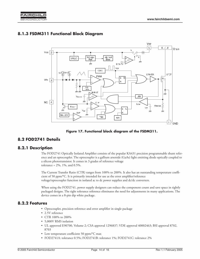
8.1.3 FSDM311 Functional Block Diagram
Figure 17. Functional block diagram of the FSDM311.
8.2 FOD2741 Details
8.2.1 Description
The FOD2741 Optically Isolated Amplifier consists of the popular KA431 precision programmable shunt refer-ence and an optocoupler. The optocoupler is a gallium arsenide (GaAs) light emitting diode optically coupled to a silicon phototransistor. It comes in 3 grades of reference voltage tolerance = 2%, 1%, and 0.5%.
The Current Transfer Ratio (CTR) ranges from 100% to 200%. It also has an outstanding temperature coeffi-cient of 50 ppm/°C. It is primarily intended for use as the error amplifier/reference voltage/optocoupler function in isolated ac to dc power supplies and dc/dc converters.
When using the FOD2741, power supply designers can reduce the component count and save space in tightly packaged designs. The tight tolerance reference eliminates the need for adjustments in many applications. The device comes in a 8-pin dip white package.
8.2.2 Features
• Optocoupler, precision reference and error amplifier in single package • 2.5V reference • CTR 100% to 200% • 5,000V RMS isolation • UL approved E90700, Volume 2; CSA approval 1296837; VDE approval 40002463; BSI approval 8702,
8703 • Low temperature coefficient 50 ppm/°C max • FOD2741A: tolerance 0.5%; FOD2741B: tolerance 1%; FOD2741C: tolerance 2%
Vcc
Vfb
NC
GND
Drain
Vstr
UVLOVoltageRef
InternalBias
OSC
PWM
S/S
15ms
BURST
OLP
LEB
lover
Vth
Rsense
SFET
Vck
8.7/6.7V
H
S Q
R
S Q
R
DRIVER
L
5µA 400µA
+
–
+
–
+
–
+
–
+
–
–
OVP
Reset
Min. 20VTSD A/R
VBURST
VSD
2
3
4
1
5 6, 7, 8
+
–
© 2005 Fairchild Semiconductor Page 15
of 16 Rev 1.1 February 2005
www.fairchildsemi.com
9. References / Resources
9.1 Application Notes
Application note AN-4137 is a full design procedure for flyback converters. Application note AN4138 is a full design procedure for a flyback charger circuit.
• AN-4137 Design Guidelines for Off-line Flyback Converters Using FPS• AN-4138 Design Considerations for Battery Charger Using Green Mode FPS• AN-4141 Troubleshooting and Design Tips for FPS Flyback Applicatons• AN-4145 Electromagnetic Compatibility for Power Converters
© 2005 Fairchild Semiconductor Page 16
of 16 Rev 1.1 February 2005
www.fairchildsemi.com
This Evaluation Board may employ high voltages so appropriate safety precautions should be used when operating this board.
Replace components on the Evaluation Board only with those parts shown on the parts list in the User's Guide. Contact an
authorized Fairchild representative with any questions.
The Evaluation Board is for demonstration purposes only and neither the Board nor this User's Guide constitute a sales contract
or create any kind of warranty, whether express or implied, as to the applications or products involved. Fairchild warranties that
its products will meet Fairchild's published specifications but does not guarantee that its products will work in any specific appli-
cation. Fairchild reserves the right to make changes without notice to any products described herein to improve reliability, func-
tion or design. Either the applicable sales contract signed by Fairchild and Buyer, or if no contract exists Fairchild's Standard
Terms and Conditions on the back of Fairchild invoices, govern the terms of sale of the products described herein.

Mouser Electronics
Authorized Distributor
Click to View Pricing, Inventory, Delivery & Lifecycle Information: Fairchild Semiconductor:
FEB100