Embed Size (px)
Citation preview
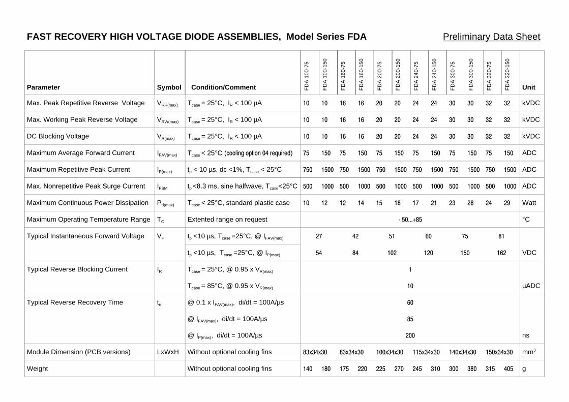
FAST RECOVERY HIGH VOLTAGE DIODE ASSEMBLIES, Model Series FDA Preliminary Data Sheet Parameter
Symbol
Condition/Comment FD
A 1
00-7
5 F
DA
100
-150
FD
A 1
60-7
5
FD
A 1
60-1
50
FD
A 2
00-7
5
FD
A 2
00-1
50
FD
A 2
40-7
5
FD
A 2
40-1
50
FD
A 3
00-7
5
FD
A 3
00-1
50
FD
A 3
20-7
5
FD
A 3
20-1
50
Unit
Max. Peak Repetitive Reverse Voltage VRR(max) Tcase = 25°C, IR < 100 µA 10 10 16 16 20 20 24 24 30 30 32 32 kVDC
Max. Working Peak Reverse Voltage VRW(max) Tcase = 25°C, IR < 100 µA 10 10 16 16 20 20 24 24 30 30 32 32 kVDC
DC Blocking Voltage VR(max) Tcase = 25°C, IR < 100 µA 10 10 16 16 20 20 24 24 30 30 32 32 kVDC
Maximum Average Forward Current IFAV(max) Tcase < 25°C (cooling option 04 required) 75 150 75 150 75 150 75 150 75 150 75 150 ADC
Maximum Repetitive Peak Current IP(max) tp < 10 µs, dc <1%, Tcase < 25°C 750 1500 750 1500 750 1500 750 1500 750 1500 750 1500 ADC
Max. Nonrepetitive Peak Surge Current IFSM tp <8.3 ms, sine halfwave, Tcase<25°C 500 1000 500 1000 500 1000 500 1000 500 1000 500 1000 ADC
Maximum Continuous Power Dissipation Pd(max) Tcase < 25°C, standard plastic case 10 12 12 14 15 18 17 21 23 28 24 29 Watt
Maximum Operating Temperature Range TO Extented range on request - 50...+85 °C
Typical Instantaneous Forward Voltage VF tp <10 µs, Tcase =25°C, @ IFAV(max) 27 42 51 60 75 81
tp <10 µs, Tcase =25°C, @ IP(max) 54 84 102 120 150 162 VDC
Typical Reverse Blocking Current IR Tcase = 25°C, @ 0.95 x VR(max) 1
Tcase = 85°C, @ 0.95 x VR(max) 10 µADC
Typical Reverse Recovery Time trr @ 0.1 x IFAV(max), di/dt = 100A/µs 60
@ IFAV(max), di/dt = 100A/µs 85
@ IP(max), di/dt = 100A/µs 200 ns
Module Dimension (PCB versions) LxWxH Without optional cooling fins 83x34x30 83x34x30 100x34x30 115x34x30 140x34x30 150x34x30 mm3
Weight Without optional cooling fins 140 180 175 220 225 270 245 310 300 380 315 405 g


![MarelliGenerators...2012/01/01 · MarelliGenerators® ASYNCHRONOUS GENERATORS Nominal output [kWA] 0 500 1000 1500 2000 428 500 600 750 1000 1500 Speed [min-1] Power range @ 50 Hz](https://img.pdfslide.us/doc/110x75/5f13bd82b474175d2177fe87/marelligenerators-20120101-marelligenerators-asynchronous-generators.jpg)