Embed Size (px)
Citation preview

3 - 1FCC ATM Controller
FCC in ATM ModeWhat youwill learn
• What is the FCC-ATM controller?• How to interface the FCC-ATM controller to a PHY• How to initialize FCC-ATM parameter RAM• How to set up the connection tables• How to set up address compression• How to interface to a CAM for address mapping• How to use a global free buffer pool• How the FCC ATM receives a cell• How to setup ATM pace control• How to initialize for various cell rates• How to process channel interrupts• How AAL0 cells are processed• What is the ATM to TDM bridging mode?• How UTOPIA 2 Operates

3 - 2FCC ATM Controller
What is ATM?Definition ATM (Asynchronous Transfer Mode) segments and multiplexes user traffic
into small, fixed-length units called cells for the purpose of providing high-speed, low-delay multiplexing and switching network to support any typeof user traffic, such as voice, data, or video applications.
Example, Layer Repre-
sentation
UserAALATM
Physical
UserAALATM
Physical
Cell Cell Cell
• AAL - ATM adaptation layer
1. Basically, an ATM station consists of four layers: user, AAL, ATM, and thephysical layer.2. On the network, communications is done in cells. Each cell originates from achannel.
Description

3 - 3FCC ATM Controller
How ATM Improves Communication PerformanceIntroduction The diagrams below compare ATM and synchronous communication. In
these diagrams, channel 1 needs to transmit at twice the rate of channel 2.
Example,ATM
UserAALATM
Physical Ch. 1Cell
Channel 1
Channel 2
UserSCC
TDM/SI
T1
Frame N
Frame N+1
Example,T1
Ch. 1Cell
Ch. 2Cell
Ch. 1Cell
Ch. 1Cell
Ch. 2Cell
Channel 1
Channel 2
Ch. 1TS
Ch. 2TS
Ch. 1TS
IdleTS
1. The slide focuses in on two channels. However, the environment has manychannels, perhaps 1000 or more.2. In the ATM example, the station can use the full bandwidth available,transmitting both channels at their required rate.3. In the T1 example, both channels can transmit at the required rate, but the fullbandwidth is not used. On the avarage, the channel 2 time slot is used only half thetime.
Description

3 - 4FCC ATM Controller
How is ATM Data ProcessedIntroduction This diagram shows how ATM data is processed.
Example User
AAL
ATM
Physical
• At the sending machine, AAL appends trailer (CS-UU) and segments theuser traffic into 48-byte units and passes them on to the ATM layer.• At the receiving machine, it accepts 48-byte units from the ATM layerand reassembles them into the original user traffic syntax.
User Data Unit
User Data Unit CS-UU
H H
Cell Cell
AALFunctions
48 bytes 48 bytes 48 bytes 48 bytes
1. Adds a header to each 48 bytes; the header contains address information.ATM LayerFunction

3 - 5FCC ATM Controller
What are VPI and VCI?Definition VPI, virtual path identifier, and VCI, virtual circuit identifier, provide the
addressing on an ATM network.
Example, Topological
Video Computer
TelecomATM
Switch
ATMSwitch
Video DataArchive
Telecom
VPI=6,VCI=1 VPI=12,VCI=12
VPI=1,VCI=28
VPI=80,VCI=7 VPI=8,VCI=16VPI=2,VCI=34
1. The VPI/VCI values are similar to data link connection identifiers (DLCIs) used inframe relay networks, and logical channel numbers (LCNs) used in X.25-basednetworks.
Description

3 - 6FCC ATM Controller
What is the FCC ATM Controller?Definition The FCC controller can transmit and receive data using ATM to a physical
device with a UTOPIA interface.
FCC,ATM Mode
FCC
Buffer DescriptorsBufferBuffer
AddressMapping
ConnectionTable
R
UTOPIAInterface
TATMAAL
• Cell processing up to 155 Mbps.
FCC, ATM Mode
PHYATMPacingControl
CH. 00CH. 01
CH. ...CH. ...
BufferBuffer
BufferBuffer
ATM data can also be transferred synchronously using the ATM-to-TDMbridging mode.
SynchronousData
1. Receive data comes from the physical device and is processed through the ATM andAAL layers.2. The address is compared within in an address mapping function to connect itthrough a channel in the connection table.3. The receive data is moved into the currently active buffer of the channel.
ReceiveDataFlow
1. When a channel needs to transmit data, the ATM pacing control puts the channel into atransmit queue.2. When the PHY device is ready to transmit a cell, it notifies transmit control whichobtains 48 bytes from the associated channel, attaches the header, and transfers the cell.
TransmitDataFlow

3 - 7FCC ATM Controller
What are the FCC ATM Pins?Introduction The diagram below shows FCC1 pins, 16 bit, master mode.
ConnectionDiagram
MPC8260FCC1
RxD[7-0]PD[27-26,24-23,21-20,15-14]
TxD[15-8]PA[18-25]RxClavPA26RxSOCPA27RxEnb*PA28TxSOCPA29TxClavPA30TxEnb*PA31
TxD[2-0]PC[10-8]
RxADDR[0-2]PC[14,12,6]
TxADDR[0-2]PC[15,13,7]
TxD[7-3]PD[28,25,22,6-5]
TxADDR[3-4]PD[7,19]
RxD[15-8]PA[17-10]
TxPrtyPD[16]RxPrtyPD[17]
RxADDR[3-4]PD[29,18]
Receive data bus
Transmit data bus
Rx Cell AvailableRx Start of CellRx EnableTx Start of CellTx Cell AvailableTx Enable
Rx Address Bus
Tx Address Bus
Tx ParityRx Parity
• There are 16 receive data pins and 16 transmit data pins. When transferring data, the oddoctets are transferred on D0-7 and the even, on D8-15.• RxClav: asserted by the PHY when it has a receive cell to transfer to the FCC.• TxClav: asserted by the PHY when it has room for a transmit cell from the FCC.• RxSOC:Active high, tristateable signal asserted by the PHY layer when RxData contains thefirst valid byte of a cell.• TxSOC: Active high signal asserted by the ATM layer when TxData contains the first validbyte of the cell.• RxEnb: active low signal asserted by the ATM layer to indicate that RxData and RxSOCwill be sampled at the end of the next cycle.• TxEnb: active low signal asserted by the ATM layer during cycles when TxData containsvalid cell data.• RxADDR: five bit wide true data driven from the ATM to MPHY layer to select theappropriate MPHY device (port in presence of multiple RxClav signals).• TxADDR:ive bit wide true data driven from the ATM to MPHY layer to poll and select theappropriate MPHY device (port in presence of multiple TxClav signals).• TxPrty: odd parity bit for 16 bits.• RxPrty: odd parity bit for 16 bits.
PinsDescription
3 - 8FCC ATM Controller
What are the FCC ATM Pin Configurations?Introduction The diagram below shows the possible FCC-ATM configurations.
ConfigurationSummary
Utopia-8 bit data busMaster or Slave
Utopia-16 bit data busMaster or Slave
FCC1
FCC2
FCC3
Yes
Yes
No
Yes
No
No
• These are the possible FCC-ATM pin configurations.• FCC1 has complete capability: 8 or 16 bits, master or slave.• FCC2 has 8-bit capability, master or slave.• FCC3 has no ATM capability.
Description

3 - 9FCC ATM Controller
PM5350
How to Interface the FCC to a PHYIntroduction The diagram below shows how to interface FCC1 to an PMC-Sierra PHY.
FCC1 is a master in 8-bit mode.
ConnectionDiagram
MPC8260FCC1
PA31/TxEnb*
PA29/TxSOCPA28/RxEnb
PA27/RxSOCPA26/RxClav
PA[18-25]/TxD[7-0]PA[17-10]/RxD[7-0]
TWREN*
PD16/TxPrtyPD17RxPrty
CLK11CLK12
PA30/TxClav TCATSOC
RSOCRRDEN*
RCATDAT[7-0]RDAT[7-0]TXPRTYRXPRTYTFCLKRFCLK
On the VADS boards, all lines have a series 43 ohm resistor. In addition,RxD[0-7], RSOC, RCA, and TCA have buffers.
PinOrdering
The UTOPIA pin ordering on the PM5350 follows the UTOPIA standard; for example,RxData[7] is the MSB.
ManagementInterface
Additional connections are required for management functions such as assigning addresses.
Some of the features of the PM5350 are:1. Compatible with the ATM Forum UTOPIA interface.2. Provides on-chip FIFO buffers in both transmit and receive paths.3. Operates at 155Mbps.4. Can operate as master or slave.
PM5350Features

3 - 10FCC ATM Controller
What is an AAL5 Cell?Definition An AAL5 cell is a basic ATM cell consisting of a 48-octet AAL PDU
(Protocol Data Unit) and a 5 octet cell header.
ExampleCell
Header PDU or payload
48 octets
53 octets
GFC VPI VCI PT/C HEC4 8 16 4 8
Supplied byuser in TCT[ATMCH] Appended by ATM
controller
1. The AAL5 cell is a standard ATM cell consisting of a header and a 48 byte payload.2. The header consists of the Header Error Control and four other fields supplied by theuser in the TCT.3. A “place holder” HEC is supplied by the ATM controller. The actual HEC iscalculated and supplied by the PHY.
• GFC - generic flow control• VPI - Virtual Path Identifier: used with the VCI to form a virtual circuit identifier.• VCI - Virtual Channel Identifier: used with VPI to form a virtual circuit identifier.• PT - payload type: identifies cell function. For example, a management cell.• C - Cell loss priority: if C=1, the cell is subject to being discarded by the network.• HEC - Header Error Control: an error check CRC on the other 4 bytes of the header; cancorrect a 1-bit error.
CellDescription
HeaderDescription

3 - 11FCC ATM Controller
What is an AAL5 Frame?Definition An AAL5 frame is one or more cells with an appended trailer in the last cell.
ExampleFrame
Cell Cell Cell LastCell
Data Padding CPCS-UU+CPI DataLength CRC32
Optional Ifrequired
Appendedto end of
last buffer
Appendedby ATMcontroller
• The last cell of a frame consists of the fields shown.• Padding is required if there is not enough data to fill the last cell.• CPCS-UU+CPI is supplied by the user for transmit.
Last CellFeatures

3 - 12FCC ATM Controller
What are the Basic FCC-ATM Structures?Definition The basic FCC-ATM structures reside in both dual port RAM and in
external memory as shown below.
MemoryMaps
Internal Memory External Memory
DPRAM1CTs,ACTs, APCTs, IQPT
DPRAM2
FCC1 Parameter RAMFCC2 Parameter RAM
DPRAM3FCC Data
Registers InterruptQueues
AddressCompression
Tables
Transmit ConnectionTables
Area forReceive & Transmit
BufferDescriptors
Receive ConnectionTables
1. The DPRAM1 area is used for Connection Tables (channels 0-255), AddressCompression Tables (virtual path), ATM Pace Control Tables, and the InterruptQueue Parameter Table.2. DPRAM2 is parameter ram for all the devices including the FCCs. FCC3 cannotdo ATM.3. DPRAM3 is a data holding area between the FIFO and the buffer.
InternalMemory
1. Buffer descriptors for all channels are in an external memory area.2. Address Compression Tables for VC are external.3. Connection Tables for channels 256-65K4. The interrupt queues.
ExternalMemory

3 - 13FCC ATM Controller
How to Locate the Buffer DescriptorsIntroduction
FCC1Memory
Map
Internal Memory External Memory
DPRAM1
DPRAM2
FCC1 Parameter RAM
DPRAM3
Registers
InterruptQueues
The diagram below shows how the Rx and Tx array spaces are located bypointers in ATM parameter RAM.
0x8400Reserved
BD_BASE_EXT0x846C
AddressCompression
Tables
Transmit ConnectionTables
Area forReceive & Transmit
BufferDescriptors
Receive ConnectionTables
0x8440
1. In this slide, we’ve highlighted the FCC1 parameter RAM area. It is located at0x8400 in the internal memory map.2. The location of the buffer descriptor area is pointed to by the parameter,BD_BASE_EXT. It is 32-bits wide, but bits 8-31 should be programmed to zero.3. Any particular channel will locate its own buffer descriptors usingBD_BASE_EXT as a base address.
Description
3 - 14FCC ATM Controller
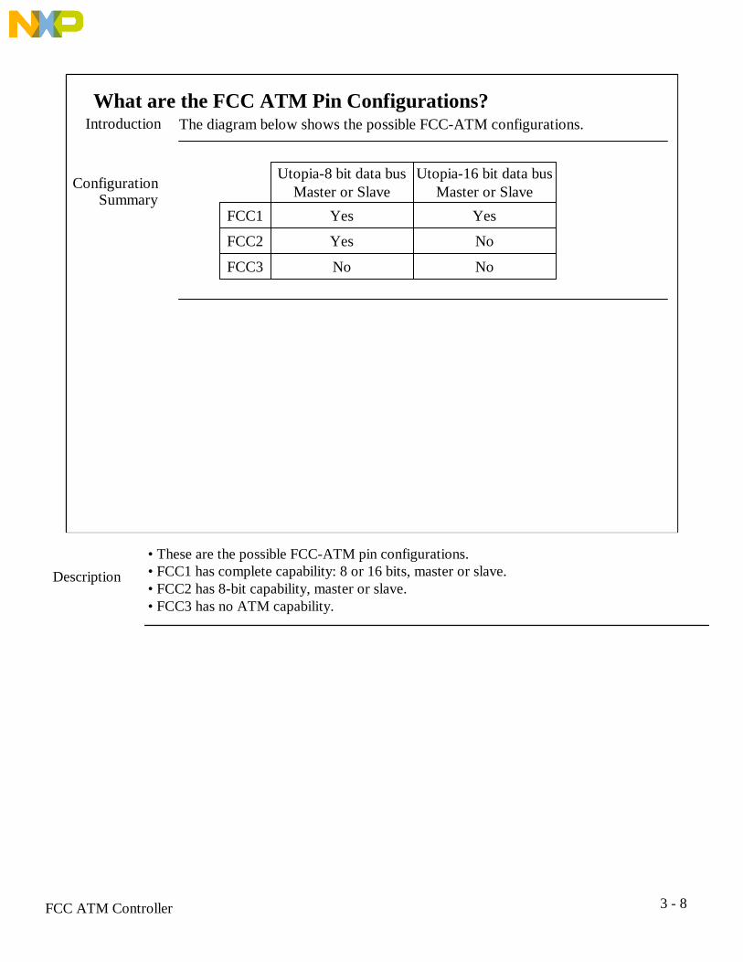
Parameter RAM Programming Model (partial)
Reserved
PRAM - FCC Parameter RAM P. 29-370 1 2 3 4 5 6 7 8 9 10 11 12 13 14 15
0
Reserved0x3E
RCELL_TMP_BASE0x40
TCELL_TMP_BASE0x42
BD_BASE_EXT0x6C
1. Here’s a part of the FCC parameter RAM programming model.2. The first 0x40 bytes are reserved and should be initialized to zero.3. RCELL and TCELL_TMP_BASE are pointers to a 52 byte area in dual portRAM for temporary data storage.4. BD_BASE_EXT is the pointer to the buffer descriptors.
Description
3 - 15FCC ATM Controller
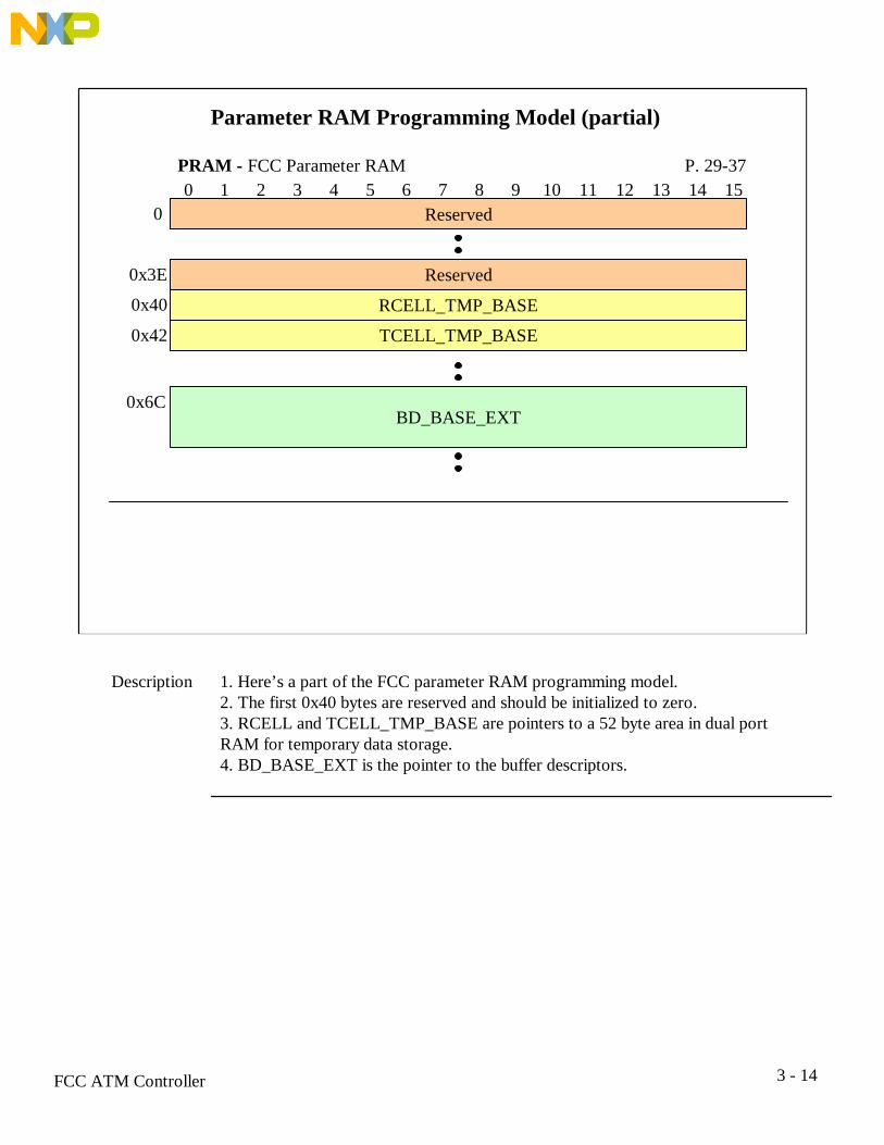
Exercise - FCC Parameter RAM
InitializeATM
ParameterRAM,FCC1
UWORD *pint; /* integer pointer */
pint = (UWORD *)(UWORD)pimm;for (i = 0; i < 0x1000; i++) /* CLEAR DPRAM1 */ *pint++ = 0;pint = (UWORD *)((UWORD)pimm + 0x8000);for (i = 0; i < 0x400; i++) /* CLEAR DPRAM2 */ *pint++ = 0;pint = (UWORD *)((UWORD)pimm + 0xB000);for (i = 0; i < 0x400; i++) /* CLEAR DPRAM3 */ *pint++ = 0;pimm->FCC1.RCELL_TMP_BASE = 0xB000; /* Rx cell temp at 0xB000 */pimm->FCC1.TCELL_TMP_BASE = ______; /* Tx cell temp next */pimm->FCC1.BD_BASE_EXT = 0x8C000000; /* BDs at 0x8C000000 */
1. The “for loops” initialize all of dual port RAM to zero.2. RCELL and TCELL_TMP_BASE are initialized to point at the DPRAM3 area.
Description
__packed__(2,2) struct immbase { /*INTRNL MEMORY MAP */ . __packed__(2,2) struct { UWORD FCC1RES[16]; /* RESERVED */ . UHWORD RCELL_TMP_BASE; /* RX CELL TEMP ADDR */ UHWORD TCELL_TMP_BASE; /* TX CELL TEMP ADDR */ . UWORD BD_BASE_EXT; . } FCC1; .};
AssumedStructures

3 - 16FCC ATM Controller
What are the Connection Tables?Definition The connection tables hold channel configuration and temporary parameters
for each channel, receive and transmit.
AddressMappingProcess
ReceiveConnection
Table BD ArraysCell
Header
FCCx
ReceiveConnectionTable Entry
ATMPace
Control
TransmitConnection
Table
BD Arrays
CellHeader
FCCx
TransmitConnectionTable Entry
1. When a cell is received, the cell header is examined by a mapping process for amatch in the connection table. If no match is found, the cell is discarded.2. If a match is found, the connection table points to a current buffer descriptor andthe 48 bytes of AAL5 cell data is written to the buffer.3. Address mapping determines the channel number.
Receive
1. When a cell is transmitted, the transmit connection table entry provides the 4 byteheader.
Transmit

3 - 17FCC ATM Controller
How to Locate the Connection TablesIntroduction
FCC1Memory
Map
Internal Memory External Memory
DPRAM1
DPRAM2
FCC1 Parameter RAM
DPRAM3
Registers
AddressCompression
Tables
Transmit ConnectionTables
InterruptQueues
0x8400
Area forReceive & Transmit
BufferDescriptors
Reserved
INT_RCT_BASEReceive Connection
Tables
TCT
RCT
INT_TCT_BASE
EXT_RCT_BASEEXT_TCT_BASE
The diagram below shows how the connection tables are located by pointers inATM parameter RAM.
1. The connection tables for channels 0-128 are located in DPRAM1 of the internalmemory. The transmit and receive CTs have their own pointer in parameter RAM.2. The internal pointers, INT_RCT_BASE and INT_TCT_BASE, are actually 16bits wide and, therefore, are offset pointers into dual port RAM.3. The connection tables for channels 256-16K are located in external memory.Again, the transmit and receive tables have their own pointer in parameter RAM.
Description
3 - 18FCC ATM Controller
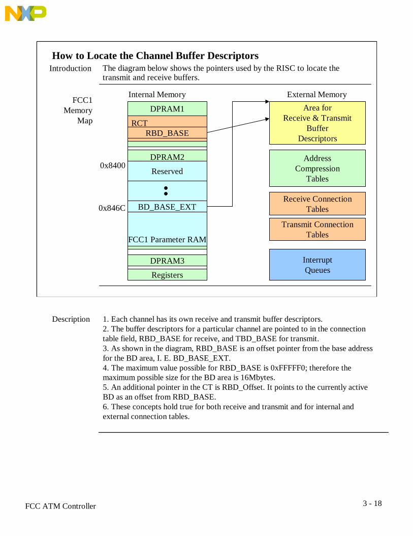
How to Locate the Channel Buffer DescriptorsIntroduction
FCC1Memory
Map
Internal Memory External Memory
DPRAM1
DPRAM2
FCC1 Parameter RAM
DPRAM3
Registers
InterruptQueues
0x8400Reserved
BD_BASE_EXT0x846C
AddressCompression
Tables
Transmit ConnectionTables
Area forReceive & Transmit
BufferDescriptors
Receive ConnectionTables
The diagram below shows the pointers used by the RISC to locate thetransmit and receive buffers.
RCTRBD_BASE
1. Each channel has its own receive and transmit buffer descriptors.2. The buffer descriptors for a particular channel are pointed to in the connectiontable field, RBD_BASE for receive, and TBD_BASE for transmit.3. As shown in the diagram, RBD_BASE is an offset pointer from the base addressfor the BD area, I. E. BD_BASE_EXT.4. The maximum value possible for RBD_BASE is 0xFFFFF0; therefore themaximum possible size for the BD area is 16Mbytes.5. An additional pointer in the CT is RBD_Offset. It points to the currently activeBD as an offset from RBD_BASE.6. These concepts hold true for both receive and transmit and for internal andexternal connection tables.
Description

3 - 19FCC ATM Controller
Connection Table Programming Model (1 of 4)
RCT - Receive Connection Table P. 29-430 1 2 3 4 5 6 7 8 9 10 11 12 13 14 15
0
RxDBPTR
- GBL BO - DT
BBIB - BU
FMSEGF
ENDF
CPUU - INTQ
2 - INF - ABRF AAL
4
Cell Time Stamp8
RBD_Offset0xC
Protocol Specific
MRBLR0x1A
RBD_BASE0x1C - PMT
0x1E RBD_BASE PM-
Description 1. The AAL field is used to select the type of frame processed by this channel. Forexample, AAL5.2. The CPUU field determines whether the received CPCS-UU+CPI field will bestored to the buffer or discarded. If stored to the buffer, it is not included in the framelength.3. RBD_BASE is an offset pointer to the receive buffer descriptors.4. DTB and BIB determine whether the SDMA to the local bus will be used or theSDMA to the 60x bus.5. GBL is for global. When set, the GBL pin will be asserted when a buffer associatedwith this connection is accessed. As a result, data cache will be snooped.

3 - 20FCC ATM Controller
Connection Table Programming Model (2 of 4)
AAL5 Specific - Receive Connection Table P. 29-450 1 2 3 4 5 6 7 8 9 10 11 12 13 14 15
TML0xE
Reserved RXBM
RxCRC0x10
RBDCNT0x14
Reserved0x16
0x18 RXFM Reserved BPOOL
Description This part of the RCT is specific to an AAL5 frame.1. RXBM determines if the receive buffer event is sent to the interrupt queue or not.2. RXFM determines if the receive frame event is sent to the interrupt queue or not.3. BPOOL selects the use of the global buffer allocation mode or not.

3 - 21FCC ATM Controller
Connection Table Programming Model (3 of 4)
TCT - Transmit Connection Table P. 29-500 1 2 3 4 5 6 7 8 9 10 11 12 13 14 15
0
TxDBPTR
- GBL BO - DT
BBIB
AVCF - ATT CP
UUVCON INTQ
2 - INF - ABRF AAL
4
TBDCNT8
Protocol Specific
TBD_Offset0xA
PCR FractionRate Remainder0xC
PCR0xE
APC Linked Channel0x16
(Continued on next page)
Description • The TCT contains many of the same parameters as the RCT; in addition it containsthe ATM pace control parameters such as Rate Remainder and APC Linked Channel.• VCON indicates when a channel has been deactivated.• CPUU enables or disables the insertion of CPCS-UU+CPI. Normally insertionwould be selected. But for a router application, for example, insertion would bedisabled

3 - 22FCC ATM Controller
Connection Table Programming Model (4 of 4)
ATMCH0x18
TBD_BASE0x1C - PMT
0x1E TBD_BASE PMIMK
STPT
BNM
TxCRC0x10
Total Message Length0x14
AAL5 Specific - Transmit Connection Table P. 29-530 1 2 3 4 5 6 7 8 9 10 11 12 13 14 15
0 1 2 3 4 5 6 7 8 9 10 11 12 13 14 15
Description 1. ATMCH is the cell header that is transmitted with each cell.2. TBD_BASE is the offset pointer to the transmit buffer descriptors.3. BNM determines if a buffer not ready event will be sent to the interrupt queue.4. IMK determines if a transmit buffer event will be sent to the interrupt queue.

3 - 23FCC ATM Controller
How to Determine a Channel’s RCT & TCTIntroduction For a given channel number, the location of its RCT and TCT can be
determined as shown below.
ConnectionTables
Locations
Dual PortRAM
INT_RCT_BASE ReservedRaw Cell(AAL0)
RCT2RCT3
ExternalRAM
EXT_RCT_BASERCT256RCT257RCT258
For channel numbers < 256:
RCT address = INT_RCT_BASE + chnum * 32
For channel numbers > 255:
RCT address = EXT_RCT_BASE + chnum * 32
1. The RCTs for channel numbers 0 to 255 reside in dual port RAM with a base addressof INT_RCT_BASE.2. The RCTs for channel numbers 256 to 65536 reside in dual port RAM with a baseaddress of EXT_RCT_BASE.3. The area from EXT_RCT_BASE to the first RCT, 256, is 8192 bytes and is availableto the user.4. For transmit, similar calculations are used with INT_TCT_BASE andEXT_TCT_BASE as the base addresses.
Findingthe CT
3 - 24FCC ATM Controller
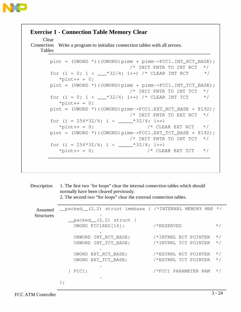
Exercise 1 - Connection Table Memory ClearClear
ConnectionTables
pint = (UWORD *)((UWORD)pimm + pimm->FCC1.INT_RCT_BASE); /* INIT PNTR TO INT RCT */for (i = 0; i < ___*32/4; i++) /* CLEAR INT RCT */ *pint++ = 0;pint = (UWORD *)((UWORD)pimm + pimm->FCC1.INT_TCT_BASE); /* INIT PNTR TO INT TCT */for (i = 0; i < ___*32/4; i++) /* CLEAR INT TCT */ *pint++ = 0;pint = (UWORD *)((UWORD)pimm->FCC1.EXT_RCT_BASE + 8192); /* INIT PNTR TO EXT RCT */for (i = 256*32/4; i < _____*32/4; i++) *pint++ = 0; /* CLEAR EXT RCT */pint = (UWORD *)((UWORD)pimm->FCC1.EXT_TCT_BASE + 8192); /* INIT PNTR TO INT TCT */for (i = 256*32/4; i < _____*32/4; i++) *pint++ = 0; /* CLEAR EXT TCT */
Write a program to initialize connection tables with all zeroes.
1. The first two ‘for loops” clear the internal connection tables which shouldnormally have been cleared previously.2. The second two “for loops” clear the external connection tables.
Description
__packed__(2,2) struct immbase { /*INTERNAL MEMORY MAP */ . __packed__(2,2) struct { UWORD FCC1RES[16]; /*RESERVED */ . UHWORD INT_RCT_BASE; /*INTRNL RCT POINTER */ UHWORD INT_TCT_BASE; /*INTRNL TCT POINTER */ . UWORD EXT_RCT_BASE; /*EXTRNL RCT POINTER */ UWORD EXT_TCT_BASE; /*EXTRNL TCT POINTER */ . } FCC1; /*FCC1 PARAMETER RAM */ .};
AssumedStructures

3 - 25FCC ATM Controller
Exercise 2 - Connection Table Entry Initialization (1 of 2)
InitializeConnection
Table
/* INITIALIZE THE RCT */prct = (rct *)((UWORD)pimm + pimm->FCC1.INT_RCT_BASE + 3 * 32); /* INIT RCT PNTR TO CT3 */prct->rcntrl1 = ______; /* INIT 1ST CNTRL FLD RCT*/prct->rcntrl2 = _; /* AAL5 CHANNEL */prct->_____ = 384; /* INIT MAX RECV BUF LNGT*/prct->_______ = 0; /* INIT RECV BD BASE PNTR*/prct->__________ = 0; /* INIT RECV BD OFST PNTR*/
Write a program to initialize connection tables for channel 3 as follows:• AAL5• Big Endian• Data buffers and interrupt queue on local bus• Use interrupt queue 2• Maximum receive buffer length is 384• RxBDs at the start of the BD areas; TxBDs at 0x1000 from start.• Transmit header is to be 0x600
(Continued on next page)
typedef __packed__(2,2) struct { UHWORD rcntrl1; /*GBL,BO,DTB,BIB,BUFM,etc.*/ UHWORD rcntrl2; /*INF,ABRF,AAL */ UWORD rxbdptr; /* RxBDPTR */ UWORD celltimestamp; /* CELL TIME STAMP */ UHWORD rbd_offset; /* RBD_Offset */ UHWORD tml; /* TOTAL MESSAGE LENGTH */ UWORD rxcrc; /* CRC32 TEMP RESULT */ UHWORD rbdcnt; /* RXBD COUNT */ UHWORD rctreserved; /* RESERVED */ UHWORD rcntrl3; /* RXBM,RXFM,BPOOL */ UHWORD mrblr; /* MAX RECV BUFFER LENGTH */ UWORD rcntrl4; /* PMT,RBD_BASE,PM */} rct; /* RECEIVE CONNECTION TBL */ /* FOR AAL5 CHANNELS */
AssumedStructure

3 - 26FCC ATM Controller
Exercise 2 - Connection Table Entry Initialization (2 of 2)
/* INITIALIZE THE TCT */ptct = (tct *)((UWORD)pimm + pimm->FCC1.INT_TCT_BASE + 3 * 32); /* INIT TCT PNTR TO CT3 */ptct->tcntrl1 = ______; /* INIT 1ST CNTRL FLD TCT*/ptct->tcntrl2 = _; /* AAL5 CHANNEL */ptct->tcntrl3 = 0x___<<4; /* INIT XMIT BD BASE PNTR*/ptct->__________ = 0; /* INIT XMIT BD OFST PNTR*/ptct->_____ = 0x600; /* INIT TCT HEADER */
typedef __packed__(2,2) struct { UHWORD tcntrl1; /*GBL,BO,DTB,BIB,AVCF,etc.*/ UHWORD tcntrl2; /*INF,ABRF,AAL */ UWORD txbdptr; /* TxBDPTR */ UHWORD tbdcnt; /* XMIT BD COUNT */ UHWORD tbd_offset; /* TBD_Offset */ UBYTE raterem; /* RATE REMAINDER */ UBYTE pcrf; /* PCR FRACTION */ UHWORD pcr; /* PEAK CELL RATE */ UWORD txcrc; /* CRC32 TEMPORARY RESULT */ UHWORD tml; /* TOTAL MESSAGE LENGTH */ UHWORD apclc; /* APC LINKED CHANNEL */ UWORD atmch; /* ATM CELL HEADER */ UWORD tcntrl3; /* PMT,TBD_BASE,BNM,etc. */} tct; /* TRANSMIT CONNECTION TBL*/ /* FOR AAL5 CHANNELS */
AssumedStructure
3 - 27FCC ATM Controller
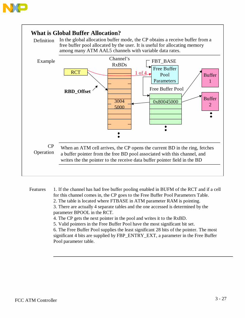
What is Global Buffer Allocation?Definition In the global allocation buffer mode, the CP obtains a receive buffer from a
free buffer pool allocated by the user. It is useful for allocating memoryamong many ATM AAL5 channels with variable data rates.
Example
RCT
30045000
0x80045000
Buffer1
Buffer2
Channel’sRxBDs
Free Buffer Pool
When an ATM cell arrives, the CP opens the current BD in the ring, fetchesa buffer pointer from the free BD pool associated with this channel, andwrites the the pointer to the receive data buffer pointer field in the BD
CPOperation
FBT_BASEFree Buffer
PoolParameters
1 of 4
RBD_Offset
1. If the channel has had free buffer pooling enabled in BUFM of the RCT and if a cellfor this channel comes in, the CP goes to the Free Buffer Pool Parameters Table.2. The table is located where FTBASE in ATM parameter RAM is pointing.3. There are actually 4 separate tables and the one accessed is determined by theparameter BPOOL in the RCT.4. The CP gets the next pointer in the pool and writes it to the RxBD.5. Valid pointers in the Free Buffer Pool have the most significant bit set.6. The Free Buffer Pool supplies the least significant 28 bits of the pointer. The mostsignificant 4 bits are supplied by FBP_ENTRY_EXT, a parameter in the Free BufferPool parameter table.
Features

3 - 28FCC ATM Controller
How to Locate the Free Buffer Pools (1 of 2)Introduction
FCC1Memory
Map
Internal Memory External Memory
DPRAM1
DPRAM2
FCC1 Parameter RAM
DPRAM3
Registers
InterruptQueues
0x8400Reserved
FBT_BASE0x8464
AddressCompression
Tables
Transmit ConnectionTables
Area forReceive & Transmit
BufferDescriptors
Receive ConnectionTables
The diagram below shows the pointers used by the RISC to locate the freebuffer pools.
Free Buffer PoolParameter Tables
Pointersto FreeBufferPointers
1. The free buffer pool parameter table is located by a pointer in parameter RAM:FBT_BASE2. Up to 4 free buffer pool parameter tables can exist. Each will have pointers to atable of free buffer pointers.
Description

3 - 29FCC ATM Controller
How to Locate the Free Buffer Pools (2 of 2)
PointerMap FBT_BASE FBP0_BASE
FBP1_BASE
FBP2_BASE
FBP3_BASE
BuffersFree BufferPool Parameters
Free BufferPointers
Dual Port RAMExternal RAM
1. Each free buffer pool parameters table has a base pointer and an active pointer toa table of free buffer pointers2. Each pointer in the free buffers pointer table points to a buffer that can be used toreceive cells.3. For a particular connection, the free buffers must be located wherever RCT[DTB]is pointing.
Description

3 - 30FCC ATM Controller
How the Free Buffer Pool Operates (1 of 2)Introduction The diagram below shows the free buffer pool.
BlockDiagram 1 0 Buffer Pointer
Buffer PointerBuffer Pointer
xxxxxxxxxxxxxxxx
Buffer PointerBuffer PointerBuffer PointerBuffer PointerBuffer PointerBuffer PointerBuffer Pointer
V W
1100001111111
0000000000001
FBPn_BASE
FBPn_PTR
CPU Pointer
n = 0 to 3
01000000000000
I
1. FBPn_BASE points to the start of a Free Buffer Pool.2. FBPn_PTR points to the next pointer that will be used by the CP.3. CPU pointer is the pointer maintained by the 603ev. It points to the place where thenext RxBD pointer will be stored after the CPU has serviced the buffer and marked itempty.
The Pointers

3 - 31FCC ATM Controller
How the Free Buffer Pool Operates (2 of 2)Introduction The diagram below shows the operation of the free buffer pool.
FlowDiagram
Start
ATM cell arrives
CP gets buffer pointer from FBPn_PTR
V=1?Y N Busy is set in Free Buffer Pool Parameter TableBusy interrupt goes to interrupt queueFCCEx.GBPB = 1
End
Clear the V bit at FBPn_PTR
Write buffer pointer to RxBD
W=1?
Increment FBPn_PTRN
Y FBPn_PTR = FBPn_BASE
End
I=1?N
Y Set RLI in Free Buffer Pool Par TblsSet FCCEx.GRLI

3 - 32FCC ATM Controller
Global Buffer Allocation Programming Model (1 of 2)
FBT_BASE
FBT_BASE - Free Buffer Pool Parameters Table Base P. 29-370 15
FBP_BASE
Free Buffer Pool Parameters Table (4 tables per ATM) P. 29-670 15
FBP_PTR
0
4
FBP_ENTRY[0-3] 0 0 0 0 0 0 0 0 0 0 0 08
FBT_ENTRY_EXTBUSY RLI Reserved PDP ReservedA
FBP_ENTRYC
1. FBP_ENTRY[0-3] contains the most significant 4 bits of the pointer that the CPwrites to the RxBD.2. The whole word at offset 8 is referred to as FBT_ENTRY_EXT.3. FBP_ENTRY stores a valid buffer pointer. It should be initialized with the firstvalid buffer pointer of the external buffer pool.4. RLI is Red Line Interrupt. It is set when the CP fetches a buffer pointer with I = 1.5. PDP - Pool Packet Discard: finish receiving any AAL5 frames in process. For newframes, don’t use this pool.
Comments

3 - 33FCC ATM Controller
Global Buffer Allocation Programming Model (2 of 2)
Free Buffer Pool Entry P. 29-670 15
Buffer Pointer
Buffer Pointer
IW-V
Res DTB BIB BUFM
SEGF
ENDF
CPUU Res INTQ0
RCT - Receive Connection Table P. 29-430 15
BOGBLReserved Res
1 2 3 4 5 6 7 8 9 10 11 12 13 14
RXFM Reserved BPOOL18 Reserved RX
BM
1. The underlined fields in the RCT are important to free buffer pool operation.2. BIB controls whether the free buffer pool resides on the 60x bus or the local bus.3. BUFM enables Global Buffer Allocation Mode for the RCT.4. BPOOL selects one of the four free buffer pools.
Comments

3 - 34FCC ATM Controller
How to Initialize for Global AllocationIntroduction The diagram below shows the procedure to initialize for global allocation.
Procedure Step Action
1
Initialize Free Buffer Pool Parameter Tables (up to 4)
FBP_BASE:fbp baseFBP_PTR:fbp pointerFBP_ENTRY_EXT:fbp entry extensionStatus:should be zeroFBP_ENTRY:fbp entry (29-67)
2
Initialize Free Buffer Pools (up to 4)V:validW:wrapI:interruptBP:buffer pointer (29-67)
3
Initialize FBT_BASE
(29-37)
1. After performing the above initialization, any RCT can enable free buffers for itselfby setting BUFM
EnablingFree Buffers

3 - 35FCC ATM Controller
What is Address Mapping?Definition Address mapping is the operation that occurs to determine the connection
through which the data from an incoming frame should be moved.
FCCxH
AddressMappingProcess
FlowDiagram
ConnectionTable
Types ofAddress
Mapping
Type GMODE[ALM]
• GMODE is a parameter in ATM parameter RAM (see page 29-41 in UM).
BD Arrays
Buffers
48 bytes of data
CellHeader
External CAM
Address Compression
0
1
1. When a cell enters the FCC’s FIFO, the header goes through a mapping process todetermine the channel with which it is associated.2. If a match is found, the associated connection table entry is checked for thelocation of the associated buffer descriptor array.3. The payload of the cell is moved to the associated buffer.
Sequenceof Events
• If no match is found, the cell is discarded.No CellFound

3 - 36FCC ATM Controller
SLTable
SLTable
SLTable
What is Address Compression Mapping?Definition Address compression mapping is a dual-level, address lookup method. It
covers the available address range while using minimum memory space.
AddressCompression
VPTable
VCTableFCCxH
CellHeader
ConnectionTable BD Arrays
Buffers
48 bytes of data
• VP (first level) is the Virtual Path Table• VC (second level) is the Virtual Connection Table
The address compression mapping method is most valuable when you areexpecting only some values for VPI/VCI. For handling all possiblecombinations, the CAM addressing method is better.
Advantage
1. VP is the first level table which contains pointers to a set of second level tables.2. VC is a second level table containing pointers to the entries in the connection tables.
TableDescription

3 - 37FCC ATM Controller
How the Address Compression Mechanism Operates
FlowDiagram
VCMASK VCOFFSET
32 bit entriesVPT_BASEVPI
VP_MASK
VP Level Address Table(resides in DPR)
Phy Addr
AC
VPpointer
equals
VCIAC
VCpointer
equals
32 bit entriesVCT_BASE
ChnumReserved16151
VC Level Address Table(resides in external memory)
MS*
1. VPI, VCI, and Phy Addr come from the incoming cell header.2. VP_MASK is in ATM parameter RAM and is initialized by the user.3. VPT_BASE and VCT_BASE are in ATM parameter RAM. They are 32-bitpointers, but the VP Level Address Table should be located in internal dual-portRAM.
ParameterLocations
1. The result is a 16-bit channel code or channel number.2. Also in the result is the MS* bit which indicates Match Successful. If the matchwas successful, this bit is zero.3. If an entry in the VP level table is not used, it must point to a VC level entry withMS = 1.
Results
1. AC stands for Address Compression.AC

3 - 38FCC ATM Controller
How Addresses are Compressed (VP Level Table)
Example Given the following parameters:
VPT_BASE = 0x320000VP_MASK = 0x365Phy + VPI = 0x236
What will VPpointer be?
0 0 0 0 0 0 1 0 0 0 1 1 0 1 1 0Phy + VPI
0 0 0 0 0 0 1 1 0 1 1 0 0 1 0 1VP_MASK
1 0 0 1 1 0
What entry in the VP Level Address Table is selected?
VPpointer
VPT_BASE + VPpointer * 4 = 0x320000 + 0x26 * 4 = 0x320098
What is the length of the VP Level Address Table?Length = (Max value of VPpointer + 1) * 4 = 0x40 *4 = 256 bytes
1. To determine the value for VPpointer, each “1” in VP_MASK is anded with itsassociated bit position in Phy + VPI and then compressed toward the least signficant bit.
VP AddressCompression

3 - 39FCC ATM Controller
How Addresses are Compressed (VC Level Table)
Example Given the following parameters:
VCT_BASE = 0x840000VCOFFSET = 0x0100VC_MASK = 0x37VCI = 0x31
What will VCpointer be?
0 0 0 0 0 0 0 0 0 0 1 1 0 0 0 1VCI
0 0 0 0 0 0 0 0 0 0 1 1 0 1 1 1VC_MASK
1 1 0 0 1
What entry in the VC Level Address Table is selected?
VCpointer
VCT_BASE + VCOFFSET * 4 + VCpointer * 4 = 0x840000 + 0x100 * 4 + 0x19 * 4 = 0x840464
What is the length of this VC Level Address Table?Length = (Max value of VCpointer + 1) * 4 = 0x20 *4 = 128 bytes
1. To determine the value for VCpointer, each “1” in VC_MASK is anded with itsassociated bit position in VCI and then compressed toward the least signficant bit.
VC AddressCompression

3 - 40FCC ATM Controller
How to Locate the Address Compression TablesIntroduction
FCC1Memory
Map
Internal Memory External Memory
DPRAM1
DPRAM2
FCC1 Parameter RAM
DPRAM3
Registers
InterruptQueues
0x8400 Reserved
VPT_BASE0x8470
Address CompressionTables (VC)
Transmit ConnectionTables
Area forReceive & Transmit
BufferDescriptors
Receive ConnectionTables
The diagram below shows the pointers used by the RISC to locate the addresscompression tables.
VP Table
VCT_BASEVPT1_BASEVCT1_BASE
VP1 Table
Address CompressionTables (VC1)
1. There are two sets of address compression tables. One set is located by twopointers in parameter RAM: VPT_BASE and VCT_BASE; these tables are for PHY#s 0-15. The other set is located by the pointers VPT1_BASE and VCT1_BASE;these tables are for PHY #s 16-31.2. VPTx_BASE is a 32-bit pointer that locates the VP table which should be in dualport RAM. It should not point to external memory because accessing 2 externallocations would result in a latency problem and a danger of overrun.3. VCTx_BASE locates the VC tables located in external memory.
Description

3 - 41FCC ATM Controller
How Address Compression Routes a Received Cell (1 of 2)Introduction The flow diagram below shows how address compression routes a received cell.
FlowDiagram
Start
Receive cell arrives
GMODE[CUAB]? 1
0
* N
Y
End
* For each 0 in VP_MASK, is the same bit position in PHY_VPI=0?** For each 0 in VC_MASK, is the same bit position in VCI=0?
VPpointer is calculatedPHY_VPI <AC> VP_MASK
GMODE[CUAB]? 1
0
** N
Y
End
A
Mis-insertedCell
Mis-insertedCell
CUABDescription
1. CUAB stands for Check Unallocated Bits. Implementing this feature guardsagainst the possibility that a mis-inserted cell can be regarded as a valid cell becausea differentiating bit is “zeroed out.”2. The first check is with PHY_VPI.3. Once VPpointer is calculated, then VC_MASK is known and VCI is checked.

3 - 42FCC ATM Controller
How Address Compression Routes a Received Cell (2 of 2)
FlowDiagram
VCpointer is calculatedVCI <AC> VC_MASK
MSB of VC entry? 1
0
End
A
VC Table Pointer is calculatedVCT_BASE + VC_OFFSET + VCpointer
Send cell to appropriate channel buffer
End
Mis-insertedCell
1. At this point, the “appropriate channel” is the channel number as stored in theVC Table. Later on, we’ll see some variations of this.
AppropriateChannel

3 - 43FCC ATM Controller
Exercise - Initializing the Address Compression Tables (1 of 8)Initialize the address compression tables for the following parameters:
PHY VPI VCICell Header Channel
Code2021
2322
2425
20x12
0x650xE4
0x1FF0x334
1
2
00
00
00
VP_MASK
3
VC_MASK VC_OFFSET
0
• VC_MASK1. For VPI=1, VC_MASK = _____________ = _____2. For VPI=2, VC_MASK = __________________ = _______
• VC_OFFSET1. For VPI=2, VC_OFFSET = length of Vctable for VPI=1 = ____________________ = ____________ = ______

3 - 44FCC ATM Controller
Exercise - Initializing the Address Compression Tables (2 of 8)
VPtableVPT_BASE 1
VCtable
0x40 Entries
0x400 Entries
VC_MASK
VC_OFFSET

3 - 45FCC ATM Controller
Exercise - Initializing the Address Compression Tables (3 of 8)Init_AC_Tables(){ UHWORD i,j; /* temporary variables */ UWORD VptEntries; /* nmbr of Vptable entries */ UWORD *pvp,*pvc; /* VP,VC table entry pointers */
pimm->FCC1._____ |= _; /* enable address compression */ /* and unallocated bit check */ pimm->FCC1.VP_MASK = _; /* init VP_MASK */
/* initialize tables for no entries */ for (i=0,j=0; i<16; i++) /* determine numbr*/ { /* of ones in */ if (pimm->FCC1._______ & (1 << i)) /* VP_MASK */ j++; } VptEntries = 1<<j; /* determine table size */ pvp = (UWORD *)(pimm->FCC1.________); /*init VPtab pntr */ for (i=0; i<VptEntries; i++) /* clear entries */ *pvp++ = 0; pvc = (UWORD *)(pimm->FCC1.________); /*init Vctab pntr */ *pvc = ______; /* init non-entry */
__packed__(2,2) struct immbase { /*INTRNL MEMORY MAP */ . __packed__(2,2) struct { UWORD FCC1RES[16]; /* RESERVED */ . UWORD VPT_BASE; /* VP TABLE BASE ADDR*/ UWORD VCT_BASE; /* VC TABLE BASE ADDR*/ . UHWORD VP_MASK; /* VP MASK */ . UHWORD GMODE; /* GLOBAL MODE ENTRY */ . } FCC1; .};
AssumedStructures

3 - 46FCC ATM Controller
Exercise - Initializing the Address Compression Tables (4 of 8)
pvp = (UWORD *)GetVPpointer(1); /*add PHY_VPI=1 to Vptable*/ *pvp = ____<<16 + 1; /*assign VCMASK/OFFSET for VPI=1*/ pvc = (UWORD *)(pimm->FCC1.VCT_BASE + 4); for (j=0; j<0x40; j++) /*init VC table to non-entry */ *pvc++ = 1<<31; pvp = (UWORD *)GetVPpointer(2); /*add PHY_VPI=2 to Vptable*/ *pvp = _____<<16 + _____; /*assign VCMASK/OFFSET for VPI=2*/ pvc = (UWORD *)(pimm->FCC1.VCT_BASE + 0x41 * 4); for (j=0; j<0x400; j++) /*init VC table to non-entry */ *pvc++ = 1<<31; /* Add the following VC entries */ /* VPI VCI Channel Code */ /* --- ------- ------------ */ /* 1 2 20 */ /* 1 0x12 21 */ /* 1 0xE4 22 */ /* 2 0x65 23 */ /* 2 0x1FF 24 */ /* 2 0x334 25 */
3 - 47FCC ATM Controller
Exercise - Initializing the Address Compression Tables (5 of 8)
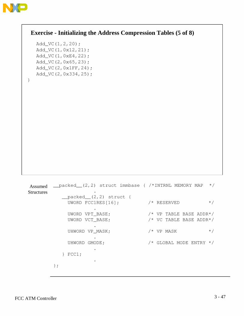
Add_VC(1,2,20); Add_VC(1,0x12,21); Add_VC(1,0xE4,22); Add_VC(2,0x65,23); Add_VC(2,0x1FF,24); Add_VC(2,0x334,25);}
__packed__(2,2) struct immbase { /*INTRNL MEMORY MAP */ . __packed__(2,2) struct { UWORD FCC1RES[16]; /* RESERVED */ . UWORD VPT_BASE; /* VP TABLE BASE ADDR*/ UWORD VCT_BASE; /* VC TABLE BASE ADDR*/ . UHWORD VP_MASK; /* VP MASK */ . UHWORD GMODE; /* GLOBAL MODE ENTRY */ . } FCC1; .};
AssumedStructures

3 - 48FCC ATM Controller
Exercise - Initializing the Address Compression Tables (6 of 8)UWORD GetVPpointer(PHY_VPI)UHWORD PHY_VPI;{ UHWORD j,k; /* temporary variables */ UWORD VPpointer; /* offset into Vptable */ UWORD *pvp; /* VP table entry pointer */
/* Calculate VPpointer for this PHY_VPI */ /* Algorithm: */ /* For each bit position, j, with a 1 in VP_MASK */ /* Anded with bit position j in PHY_VPI */ /* Put result into bit position k of VPpointer */ for (j=0,k=0; j<32; j++) if (pimm->FCC1._______>>j & 1 == 1) /*if mask bit=1 */ { VPpointer |= (_______>>j & 1)<<k; /*and-result to */ k++; /*VP pointer */ } pvp = (UWORD *)(pimm->FCC1.________ + VPpointer*4); return(pvp);}
__packed__(2,2) struct immbase { /*INTRNL MEMORY MAP */ . __packed__(2,2) struct { UWORD FCC1RES[16]; /* RESERVED */ . UWORD VPT_BASE; /* VP TABLE BASE ADDR*/ UWORD VCT_BASE; /* VC TABLE BASE ADDR*/ . UHWORD VP_MASK; /* VP MASK */ . UHWORD GMODE; /* GLOBAL MODE ENTRY */ . } FCC1; .};
AssumedStructures

3 - 49FCC ATM Controller
Exercise - Initializing the Address Compression Tables (7 of 8)Add_VC(PHY_VPI,VCI,chno)UHWORD PHY_VPI,VCI,chno;{ UHWORD j,k; /* temporary variables */ UWORD VCpointer; /* offset into VCtable */ UWORD *pvp,*pvc; /* VP,VC table entry pointers */ UHWORD VC_MASK,VC_OFFSET; /* VC mask, VC offset */
pvp = (UWORD *)GetVPpointer(PHY_VPI); VC_MASK = *pvp>>16; VC_OFFSET = *pvp & 0xFFFF;/* Calculate VCpointer for this VCI */ /* Algorithm: */ /* For each bit position, j, with a 1 in VC_MASK */ /* Anded with bit position j in VCI */ /* Put result into bit position k of VCpointer */

3 - 50FCC ATM Controller
Exercise - Initializing the Address Compression Tables (8 of 8)
for (j=0,k=0; j<32; j++) if (_______ >>j & 1 == 1) /* if the mask bit = 1 */ { VCpointer |= (___>>j & 1)<<k; /*and-result to */ k++; /*VC pointer */ } pvc = (UWORD *)(pimm->FCC1.________ + _________*4 + VCpointer*4); /*init pointer to VC table entry */ *pvc = ____; /* assign channel number to VC entry*/}
__packed__(2,2) struct immbase { /*INTRNL MEMORY MAP */ . __packed__(2,2) struct { UWORD FCC1RES[16]; /* RESERVED */ . UWORD VPT_BASE; /* VP TABLE BASE ADDR*/ UWORD VCT_BASE; /* VC TABLE BASE ADDR*/ . UHWORD VP_MASK; /* VP MASK */ . UHWORD GMODE; /* GLOBAL MODE ENTRY */ . } FCC1; .};
AssumedStructures

3 - 51FCC ATM Controller
What is CAM Mapping?Definition When a CAM is used for address mapping, the cell header is written to the
CAM and a subsequent read obtains the channel code.
FCCxH
CAM
FlowDiagram
ConnectionTable BD Arrays
Buffers
48 bytes of data
CellHeader
DataFormats
Data Write:
Phy Addr GFC + VPI VCI4 12 16
Data Read:
Channel Code1 15 16
MS*
1. As with address compression, MS* indicates if there was a successful match (1 meansno match).
MS

3 - 52FCC ATM Controller
MCM69C232
How to Interface a CAM to the PQ2Introduction The diagram below shows how to interface the MCM69C232 to the
PowerQUICC 2. For more information, go to the Web page.
ConnectionDiagram
MPC8260 A[2-0]A[25-27]MQ[31-0]D[0-31]
GCSy
LH/SM
DQ[15-0]
WEBCTL0CSx
RESET
SEL
POE*/PSDRAS*/PGPL2
PWE[0]*/PSDDQM[0]*/PBS[0]*
PORESET
KMODEDelay
KCLKIN
ClockSource
1. The 69C232 has two separate ports: control and match.2. For control operations, CSx and DQ[0-15] are used. The control mode is used to setupvarious functions of the CAM and to initialize the entries.3. For match operations, Csy and MQ[0-31] are used. The match operation is used whena header needs to be matched for a channel code.
BasicFeatures

3 - 53FCC ATM Controller
How the Channel Code Points to the RCTIntroduction The channel number resulting from the address lookup is a 16-bit value
which determines the Receive Connection Table entry to be used.
ConnectionTables
Locations
Dual PortRAM
INT_RCT_BASE ReservedRaw Cell(AAL0)
RCT2RCT3
ExternalRAM
EXT_RCT_BASERCT256RCT257RCT258
For channel codes < 256:
RCT address = INT_RCT_BASE + chnum * 32
For channel codes > 255:
RCT address = EXT_RCT_BASE + chnum * 32
1. Once the channel code has been retrieved, it must be used to access the associatedRCT.2. The RCTs for channel codes 0 to 255 reside in dual port RAM with a base address ofINT_RCT_BASE.3. The RCTs for channel codes 256 to 65536 reside in external memory with a baseaddress of EXT_RCT_BASE.4. The RCT’s parameter, RBD_Offset, points to the current buffer descriptor and thepayload is moved to its buffer.5. For transmit, similar calculations are used with INT_TCT_BASE andEXT_TCT_BASE as the base addresses.
Findingthe RCT

3 - 54FCC ATM Controller
How the FCC Receives an AAL5 Cell (1 of 3)Introduction The flow diagram below shows the AAL5 receive operation.
FlowDiagram
Start
A
A PHY asserts RxClav, UTOPIA I/F asserts RxEnb, and a complete cell is read into the FIFO
CP reads cell header and performs lookup, AC or CAM
Matchfound?
N Cell is discarded;UNI statistics tables
are updated EndY
Chno > 255 CP commands DMA tofetch RCT parameters
Y
N
BeforeReceive
Starts
Host must:1. Create ATM memory structure.2. Initialize buffer descriptors.3. Write pointer of first BD into RCT.
• In slave mode, RxCLAV is asserted when the FCC can receive a complete cell.• In master mode, RxCLAV is asserted by the PHY when it has a complete cell topass on to the FCC.• Any of 4 RxCLAV signals might be asserted, depending on the polling mode used.
Assertionof RxCLAV

3 - 55FCC ATM Controller
How the FCC Receives an AAL5 Cell (2 of 3)
FlowDiagram(cont’d)
A
Receiver goesto hunt mode
End
BTM copies cell to RCELL_TMP_BASE
DMA copies datafrom DPR to buffer
Recvbuffer empty
?
Y
B
NBSY is set
ReceiverGoes to
HuntMode
• When receiver goes into hunt mode, any remaining cells associated with the frameare discarded.• The receiver will not attempt to open a new buffer until the start of another frame.• When this occurs, an interrupt entry will be created in the interrupt queue (if notmasked) with the BSY bit set.

3 - 56FCC ATM Controller
How the FCC Receives an AAL5 Cell (3 of 3)
FlowDiagram(cont’d)
B
EOFram? N
Y
Set appropriate status bits in RxBD
RCT[CPUU]=1?
N
Y Copy CPCS-UU+CPIto buffer
End
End
RxBDStatus
Bits
Possible bits that might be set in the RxBD are:• L = last in frame• F = first in frame• CLP = cell loss priority:set if at least one cell in the frame was received with CLP=1in the header• CNG = congestion indication:set if the last cell was received with the the middle PTIbit set in the header.• ABRT = abort message indication: the length field was zero.• CPUU = CPCS-UU+CPI copying enabled.• LNE = Rx length error: pad length was > 47 or < 0.• CRE = Rx CRC error.
3 - 57FCC ATM Controller
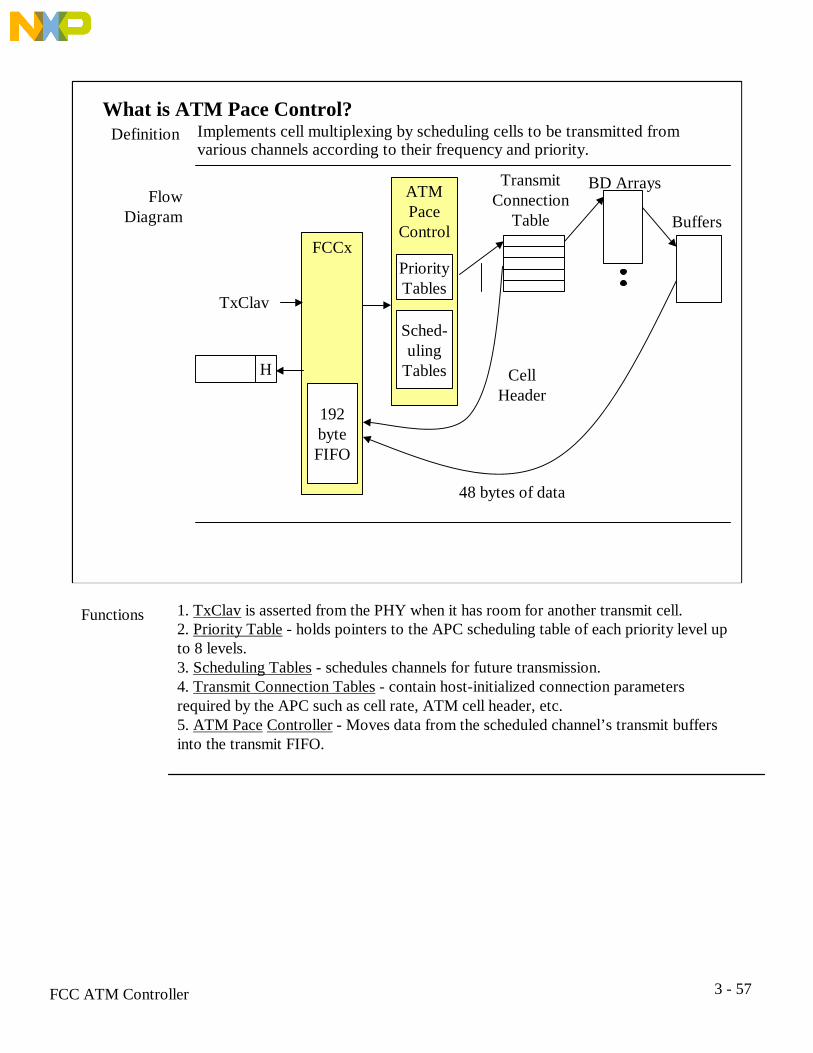
What is ATM Pace Control?Definition
FCCx
H
ATMPace
Control
FlowDiagram
TransmitConnection
Table
BD Arrays
Buffers
48 bytes of data
CellHeader
PriorityTables
Sched-uling
Tables
Implements cell multiplexing by scheduling cells to be transmitted fromvarious channels according to their frequency and priority.
TxClav
192byteFIFO
Functions 1. TxClav is asserted from the PHY when it has room for another transmit cell.2. Priority Table - holds pointers to the APC scheduling table of each priority level upto 8 levels.3. Scheduling Tables - schedules channels for future transmission.4. Transmit Connection Tables - contain host-initialized connection parametersrequired by the APC such as cell rate, ATM cell header, etc.5. ATM Pace Controller - Moves data from the scheduled channel’s transmit buffersinto the transmit FIFO.

3 - 58FCC ATM Controller
How the Basic APC Structures InteractIntroduction
FCCx
ATM Pace Control
InteractionDiagram
ConnectionTable
48 bytes of data
CellHeader
The diagram below shows the relationship between the basic APCstructures.
SchedulingTables
APCParam-etersAPC
Param-eters
(up to 31PHYs)
Channel Number(s)
PriorityTables
APCParameter
Tables
192byteFIFO
Priority 1
Priority 2
Priority 3
Priority 4
Priority 8
TableFunctions
1. APC Parameters Tables define the number of priority levels to process and numberof cells to be sent per APC time slot.2. Priority Tables specify the endpoints of the scheduling tables plus the real pointersand the service pointers.3. Scheduling Tables hold the channel numbers which have cells to be transmitted intheir scheduled order.

3 - 59FCC ATM Controller
How to Locate the ATM Pace Control TablesIntroduction
FCC1Memory
Map
Internal Memory External Memory
DPRAM1
DPRAM2
FCC1 Parameter RAM
DPRAM3
Registers
InterruptQueues
0x8400 Reserved
APCP_BASE0x8462
AddressCompression
Tables
Transmit ConnectionTables
Area forReceive & Transmit
BufferDescriptors
Receive ConnectionTables
The diagram below shows the pointers used by the RISC to locate the ATMpace control tables.
APC Param Table(s)
Priority Table(s)
Scheduling Table(s)
1. APCP_BASE in parameter RAM locates the base of the APC parameter table(s)in dual port RAM. There may be up to 32 APC parameter tables, one for each PHY.A particular table is located at ACPC_BASE + PHY_NO*32.2. Each APC parameter table points to up to 8 priority tables.3. Each priority table points to a scheduling table.
Description

3 - 60FCC ATM Controller
How the APC Operates (1 of 2)Introduction The general flow diagram below shows the operation of the APC.
FlowDiagram
Start
TxClav asserts
Transmit highest priority cell
Transmit idle cellN
Y
(1)
(2)
Increment RPs;clear cell counter
Y
N
Increment cell counter
A
(1) Any service pointerpointing at a slot with achannel number?
(2) Is cell counter = CPS?

3 - 61FCC ATM Controller
How the APC Operates (2 of 2)
FlowDiagram(cont’d)
End
(1) NIncrement each SP to its RPor to next slot with a channel
number
Y
A
(1) Any service pointerpointing at a slot with achannel number?

3 - 62FCC ATM Controller
APC Example (1 of 9)
SchedulingTable
RP1 = Real-time Pointer 1 = APC_LEV1_RPTRRP2 = Real-time Pointer 2 = APC_LEV2_RPTRSP1 = Service Pointer 1 = APC_LEV1_SPTRSP2 = Service Pointer 2 = APC_LEV2_SPTR
• The scheduling tableis 8 time slots long.• CPS = 2, i.e. 2channels per time slotmaximum.
TransmitConnection
Table
A2,1 B3 C
DEFGH
RP1,SP1CBR Table
ABC
4,5,6 DEFGH
RP2,SP2UBR Table
Ch #123456
Kind of ServiceCBRCBRCBRUBRUBRUBR
Period223444
Cell Counter = 0
1. As a example to show how the scheduling works, we have two schedulingtables: 1) a high priority table for constant bit rate channels and 2) a low prioritytable for unspecified bit rate channels.2. Channels 1 and 2 are scheduled in time slot B of the CBR table, and channel 3 isin time slot C of the same table. Channels 4, 5, and 6 are scheduled in time slot Dof the UBR table.3. The real-time pointers and the service pointers for each table are pointed at slotA.4. The cell counter is zero.5. In the Transmit connection Table, channels 1 and 2 have a period of 2, channel 3a period of 3, and the rest of the channels a period of 4.
The Setup

3 - 63FCC ATM Controller
APC Example (2 of 9)InitialState
SchedulingTable
State #1 TxClav asserts:1. PowerQUICC 2 transmits an idle cell (no service pointer pointing at aslot with a channel number).2. Cell counter increments to 1.
A2,1 B3 C
DEFGH
RP1,SP1CBR Table
ABC
4,5,6 DEFGH
RP2,SP2UBR Table
A2,1 B3 C
DEFGH
CBR TableABC
4,5,6 DEFGH
UBR TableRP1,SP1 RP2,SP2
1. In state 1, because no service pointer was pointing at a channel, an idle cell wastransmitted.2. Because the result of incrementing the cell counter was not CPS, the real-time pointerdoes not change.3. Because the service pointer points to the same place as the real-time pointer, it doesnot change.
Description

3 - 64FCC ATM Controller
APC Example (3 of 9)
State #2TxClav asserts:1. PowerQUICC 2 transmits an idle cell.2. Cell counter increments to two and then to zero because CPS=2.
A2,1 B3 C
DEFGH
CBR TableABC
4,5,6 DEFGH
UBR Table
RP1,SP1 RP2,SP2
State #3TxClav asserts:1. PowerQUICC 2 transmits a channel 2 cell and reschedules channel 2.2. Cell counter increments to 1.
A1 B3 C2 D
EFGH
CBR TableABC
4,5,6 DEFGH
UBR Table
RP1,SP1 RP2,SP2
1. TxClav asserts, moving the APC to state #2.2. Because no service pointer was pointing at a channel, an idle cell was transmitted.3. The result of incrementing the cell counter was that the count reached the value ofCPS; therefore, the cell counter is made 0 and the RPs are incremented.4. Because no service pointer is pointing to a slot which contains a channel number, theSPs are moved to the RPs.
State #2Description
1. TxClav asserts, moving the APC to state #3.2. In state 3, because the first service pointer was pointing at a channel, a channel 2 cellis transmitted. Channel 2 is rescheduled to slot D.3. Because the result of incrementing the cell counter was not CPS, the real-time pointerdoes not change.4. Because the service pointer points to the same place as the real-time pointer, it doesnot change.
State #3Description

3 - 65FCC ATM Controller
APC Example (4 of 9)
State #4TxClav asserts:1. PowerQUICC 2 transmits a channel 1 cell and reschedules channel 1.2. Cell counter increments to two and then to zero because CPS=2.
AB
3 C2,1 D
EFGH
CBR TableABC
4,5,6 DEFGH
UBR Table
RP1,SP1 RP2,SP2
State #5TxClav asserts:1. PowerQUICC 2 transmits a channel 3 cell and reschedules channel 3.2. Cell counter increments to 1.
ABC
2,1 DE
3 FGH
CBR TableABC
4,5,6 DEFGH
UBR Table
RP1,SP1 RP2,SP2
1. TxClav asserts, moving the APC to state #4.2. Because the first service pointer was pointing at a channel, a channel 1 cell istransmitted. Channel 1 is rescheduled to slot D.3. The result of incrementing the cell counter was that the count reached the value ofCPS; therefore, the cell counter is made 0 and the RPs are incremented.4. Because no service pointer is pointing to a slot which contains a channel number, theSPs are moved to the RPs.
State #4Description
1. TxClav asserts, moving the APC to state #5.2. In state 5, because the first service pointer was pointing at a channel, a channel 3 cellis transmitted. Channel 3 is rescheduled to slot F.3. Because the result of incrementing the cell counter was not CPS, the real-time pointerdoes not change.4. Because the service pointer points to the same place as the real-time pointer, it doesnot change.
State #5Description

3 - 66FCC ATM Controller
APC Example (5 of 9)
State #6TxClav asserts:1. PowerQUICC 2 transmits an idle cell.2. Cell counter increments to two and then to zero because CPS=2.
ABC
2,1 DE
3 FGH
CBR TableABC
4,5,6 DEFGH
UBR Table
RP1,SP1 RP2,SP2
State #7TxClav asserts:1. PowerQUICC 2 transmits a channel 2 cell and reschedules channel 2.2. Cell counter increments to 1.
ABC
1 DE
3,2 FGH
CBR TableABC
4,5,6 DEFGH
UBR Table
RP1,SP1 RP2,SP2
1. TxClav asserts, moving the APC to state #6.2. Because no service pointer was pointing at a channel, an idle cell is transmitted.3. The result of incrementing the cell counter was that the count reached the value ofCPS; therefore, the cell counter is made 0 and the RPs are incremented.4. Because no service pointer is pointing to a slot which contains a channel number, theSPs are moved to the RPs.
State #6Description
1. TxClav asserts, moving the APC to state #7.2. In state 7, because the first service pointer was pointing at a channel, a channel 2 cellis transmitted. Channel 2 is rescheduled to slot F.3. Because the result of incrementing the cell counter was not CPS, the real-time pointerdoes not change.4. Because the service pointer points to the same place as the real-time pointer, it doesnot change.
State #7Description

3 - 67FCC ATM Controller
APC Example (6 of 9)
State #8TxClav asserts:1. PowerQUICC 2 transmits a channel 1 cell and reschedules channel 1.2. Cell counter increments to two and then to zero because CPS=2.
ABCDE
3,2,1 FGH
CBR TableABC
4,5,6 DEFGH
UBR Table
SP2
State #9TxClav asserts:1. PowerQUICC 2 transmits a channel 4 cell and reschedules channel 4.2. Cell counter increments to 1.
ABCDE
3,2,1 FGH
CBR TableABC
5,6 DEFG
4 H
UBR Table
SP2
SP1,RP1 RP2
SP1,RP1 RP2
1. TxClav asserts, moving the APC to state #8.2. Because the first service pointer was pointing at a channel, a channel 1 cell istransmitted. Channel 1 is rescheduled to slot F.3. The result of incrementing the cell counter was that the count reached the value ofCPS; therefore, the cell counter is made 0 and the RPs are incremented.4. SP1 is incremented to RP1; SP2 remains because it is pointing at a slot which containsa channel number.
State #8Description
1. TxClav asserts, moving the APC to state #9.2. In state 9, because the second service pointer was pointing at a channel, a channel 4cell is transmitted. Channel 4 is rescheduled to slot H.3. Because the result of incrementing the cell counter was not CPS, the real-time pointerdoes not change.4. Because SP1 is already at RP1, SP1 does not change. Because SP2 still points at a slotwith a channel number in it, it does not change.
State #9Description

3 - 68FCC ATM Controller
APC Example (7 of 9)
State #10TxClav asserts:1. PowerQUICC 2 transmits a channel 5 cell and reschedules channel 5.2. Cell counter increments to two and then to zero because CPS=2.
ABCDE
3,2,1 FGH
CBR TableABC
6 DEFG
4,5 H
UBR Table
SP2
State #11TxClav asserts:1. PowerQUICC 2 transmits a channel 3 cell and reschedules channel 3.2. Cell counter increments to 1.
3 ABCDE
2,1 FGH
CBR TableABC
6 DEFG
4,5 H
UBR Table
SP1,RP1 RP2
SP1,RP1 RP2
SP2
1. TxClav asserts, moving the APC to state #10.2. Because the second service pointer was pointing at a channel, a channel 5 cell istransmitted. Channel 5 is rescheduled to slot H.3. The result of incrementing the cell counter was that the count reached the value ofCPS; therefore, the cell counter is made 0 and the RPs are incremented.4. Because SP1 was not pointing at a slot with a channel number, it is incremented toRP1. SP2 remains because it is pointing at a slot with a channel number.
State #10Description
1. TxClav asserts, moving the APC to state #11.2. In state 11, because the first service pointer was pointing at a channel, a channel 3 cellis transmitted. Channel 3 is rescheduled to slot A.3. Because the result of incrementing the cell counter was not CPS, the real-time pointerdoes not change.4. Because no service pointer points are pointing to slots with channel numbers, theyremain unchanged.
State #11Description

3 - 69FCC ATM Controller
APC Example (8 of 9)
State #12TxClav asserts:1. PowerQUICC 2 transmits a channel 2 cell and reschedules channel 2.2. Cell counter increments to two and then to zero because CPS=2.
3 ABCDE
1 FG
2 H
CBR TableABC
6 DEFG
4,5 H
UBR Table
SP1
SP2
State #13TxClav asserts:1. PowerQUICC 2 transmits a channel 1 cell and reschedules channel 1.2. Cell counter increments to 1.
3 ABCDEFG
2,1 H
CBR TableABC
6 DEFG
4,5 H
UBR Table
SP2
RP1 RP2
SP1,RP1 RP2
1. TxClav asserts, moving the APC to state #12.2. Because the first service pointer was pointing at a channel, a channel 2 cell istransmitted. Channel 2 is rescheduled to slot H.3. The result of incrementing the cell counter was that the count reached the value ofCPS; therefore, the cell counter is made 0 and the RPs are incremented.4. Because the service pointers are pointing to a slot which contains a channel number,the SPs are not changed.
State #12Description
1. TxClav asserts, moving the APC to state #13.2. In state 13, because the first service pointer was pointing at a channel, a channel 1 cellis transmitted. Channel 1 is rescheduled to slot H.3. Because the result of incrementing the cell counter was not CPS, the real-time pointerdoes not change.4. Because SP1 points to a slot which contains a channel number, the it is incremented toRP1. SP2 remains unchanged.
State #13Description

3 - 70FCC ATM Controller
APC Example (9 of 9)
State #14TxClav asserts:1. PowerQUICC 2 transmits a channel 6 cell and reschedules channel 6.2. Cell counter increments to two and then to zero because CPS=2.
3 ABCDEFG
2,1 H
CBR TableABCDEFG
4,5,6 H
UBR Table
Summary
SP1,RP1 SP2,RP2
TransmitRPSP
idle idleincinc
TxClav
2 1incinc
3 idleincinc
2 1inc
inc 1
4 5inc
inc 1
6
A-1&2 B-3&4 C-5&6 D-7&8 E-9&10Slot Entry
1. TxClav asserts, moving the APC to state #14.2. Because the second service pointer was pointing at a channel, a channel 6 cell istransmitted. Channel 6 is rescheduled to slot H.3. The result of incrementing the cell counter was that the count reached the value ofCPS; therefore, the cell counter is made 0 and the RPs are incremented.4. Because no service pointer is pointing to a slot which contains a channel number, theSPs are moved to the RPs.
State #14Description
1. Each time TxClav occurs, a cell is transmitted. If no channel has a cell available, thenthe APC transmits an idle cell.2. The RPs are incremented every time CPS assertions of TxClav occurs.3. When an SP is pointing at a slot which does not contain a channel number, the SPs areincremented to either the next slot with a channel number or to the RPs.
SummaryDescription

3 - 71FCC ATM Controller
How to Determine the Scheduling Table Size (1 of 3)Introduction
CPS
Example
The sheet describes how to calculate the scheduling table size.
• The VC(s) with the maximum bit rate can be scheduled every time slot,i.e. in the TCT it will have a period of 1.• The number of cells that can be transmitted within a time slot (CPS) is:
CPS = PHY max bit rate/VC max bit rate
If PHY max bit rate/VC max bit rate = 4, then the maximum VC rate can beobtained if CPS = 4.
SlotTimeout
TxCav
TransmitVCmax
Transmitother VCs
TxD
1. This example shows that a VC which is transmit at the maximum rate will have 1cell transmitted every time slot.

3 - 72FCC ATM Controller
How to Determine the Scheduling Table Size (2 of 3)Scheduling
TableLength
• If M is the table length, then(M-1) * CPS = PHY max bit rate/VC min bit rate.
5For example:If channel 5 is a VC min rate and CPS=1,then it will have a period of 7 in the TCT.When it is rescheduled, it advances by thelength of the table - 1.
• The VC min rate is obtained when the VC is transmitted once every scanof the table.
Determiningthe Length
If PHY max bit rate/VC min bit rate = 16, then for channels to operate at themin transmit rates, CPS vs. M vs. P (period) is:
CPS M P1 17 162 9 83 7 5.334 5 4

3 - 73FCC ATM Controller
How to Determine the Scheduling Table Size (3 of 3)
Slot
TxCav
TransmitVCmin
Transmitother VCs
TxD
Example

3 - 74FCC ATM Controller
ATM Pace Control Programming Model (1 of 2)
APCPT - APC Parameters Table P. 29-610 1 2 3 4 5 6 7 8 9 10 11 12 13 14 15
0
2
4
8
APCL_FIRST
0xC
CPS
APCL_LAST
APCL_PTR
CPS_CNT6
MAX_ITERATION CPS_ABR
LINE_RATE_ABR0xA
REAL_TSTP
APC_STATE0x10
1. APCL_FIRST and LAST define the number of priority tables. APCL_PTR points atthe presently active priority table.2. CPS specifies cells per slot.
Description

3 - 75FCC ATM Controller
ATM Pace Control Programming Model (2 of 2)
APTE - APC Priority Table Entry P. 29-620 1 2 3 4 5 6 7 8 9 10 11 12 13 14 15
0
2
4
APC_LEVi_BASE
APC_LEVi_END
APC_LEVi_RPTR
6 APC_LEVi_SPTR
Control Slot P. 29-620 1 2 3 4 5 6 7 8 9 10 11 12 13 14 15
0 All ZeroesTCTE
1. APC_LEVi_BASE and END define the length of the scheduling table.2. APC_LEVi_RPTR and SPTR are the real-time pointers and the service pointers.
APTE
1. The control slot is the last slot in the scheduling table.1. TCTE indicates use of external VBR, ABR, UBR+ channels.
TCTE

3 - 76FCC ATM Controller
Example (1 of 2)
Problem
CPS = PHY / VMAX = 25.6Mbps/2.56Mbps = 10
(M-1) * CPS = PHY/VMIN = 25.6 Mbps/64Kbps = 400
Since VCC max is unspecified, we first determine a value for (M-1) * CPS:
and then choose a suitable value for VMAX, say 2.56Mbps:
and then:M = (400/CPS) + 1 = 41
ExampleSolution
papc = (apc *)((UWORD)pimm + pimm->FCC1.APCP_BASE);papc->apcl_first = 0x300; /* LOCATE CBR TABLE AT 0x300*/papc->apcl_last = 0x308; /* LOCATE START OF UBR TABLE*/papc->apcl_ptr = papc->apcl_first; /* INIT CURR ENTRY POINTER */papc->cps = 9; /* INIT CELLS PER SLOT */
(Continued on next page)
A system has a PHY bit rate of 25.6 Mbps. The minimum VCC bit rate is64Kbps. The high priority table (CBR) is to be located at 0x300 in dual portRAM, the low priority table right on top of it. The scheduling tables are nextto the low priority table. First determine the values for CPS and M and thencomplete the initialization program.
typedef __packed__(2,2) struct { UHWORD apcl_first; /* ADDR OF 1ST PRI TBL */ UHWORD apcl_last; /* ADDR OF LAST PRI TBL */ UHWORD apcl_ptr; /* ADDR OF CURRENT PRI TBL*/ UBYTE cps; /* CELLS PER SLOT - 1 */ UBYTE cps_cnt; /*CELLS SENT PER SLOT CNTR*/ UBYTE max_iteration; /*MAX NMBR OF SCAN ITERATS*/ UBYTE cps_abr; /* ABR CELLS PER SLOT */ UHWORD line_rate_abr; /* ABR PHY LINE RATE */ UWORD real_tstp; /* REAL-TIME STAMP POINTER*/ UWORD apc_state; /* USED INTERNALLY */} apc; /* APC PARAMETERS TBL */
AssumedStructure
3 - 77FCC ATM Controller
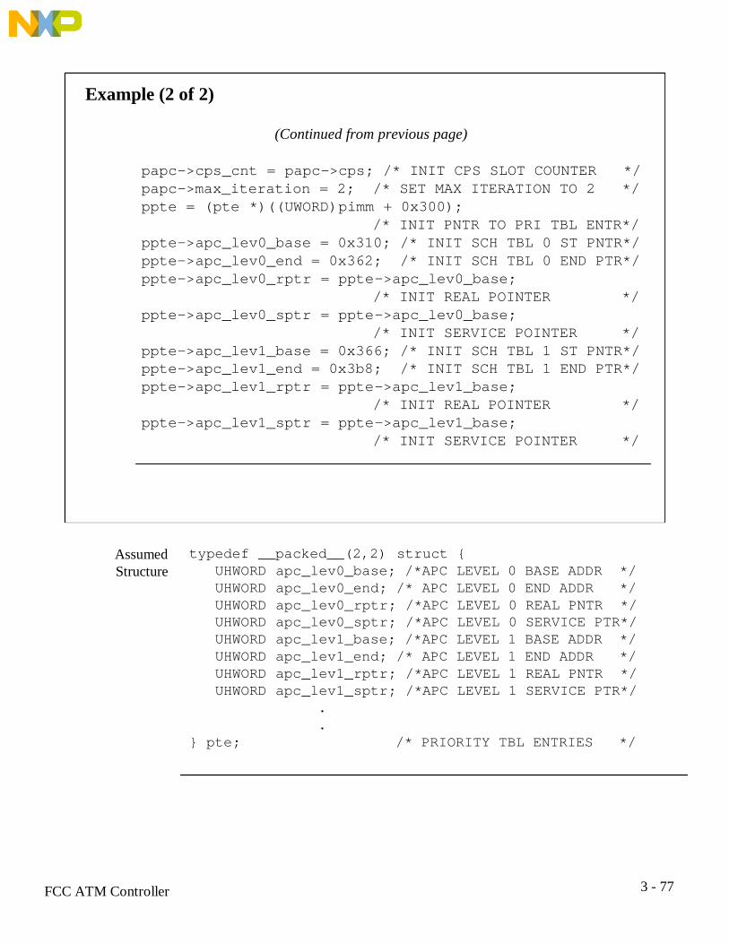
Example (2 of 2)
papc->cps_cnt = papc->cps; /* INIT CPS SLOT COUNTER */papc->max_iteration = 2; /* SET MAX ITERATION TO 2 */ppte = (pte *)((UWORD)pimm + 0x300); /* INIT PNTR TO PRI TBL ENTR*/ppte->apc_lev0_base = 0x310; /* INIT SCH TBL 0 ST PNTR*/ppte->apc_lev0_end = 0x362; /* INIT SCH TBL 0 END PTR*/ppte->apc_lev0_rptr = ppte->apc_lev0_base; /* INIT REAL POINTER */ppte->apc_lev0_sptr = ppte->apc_lev0_base; /* INIT SERVICE POINTER */ppte->apc_lev1_base = 0x366; /* INIT SCH TBL 1 ST PNTR*/ppte->apc_lev1_end = 0x3b8; /* INIT SCH TBL 1 END PTR*/ppte->apc_lev1_rptr = ppte->apc_lev1_base; /* INIT REAL POINTER */ppte->apc_lev1_sptr = ppte->apc_lev1_base; /* INIT SERVICE POINTER */
(Continued from previous page)
typedef __packed__(2,2) struct { UHWORD apc_lev0_base; /*APC LEVEL 0 BASE ADDR */ UHWORD apc_lev0_end; /* APC LEVEL 0 END ADDR */ UHWORD apc_lev0_rptr; /*APC LEVEL 0 REAL PNTR */ UHWORD apc_lev0_sptr; /*APC LEVEL 0 SERVICE PTR*/ UHWORD apc_lev1_base; /*APC LEVEL 1 BASE ADDR */ UHWORD apc_lev1_end; /* APC LEVEL 1 END ADDR */ UHWORD apc_lev1_rptr; /*APC LEVEL 1 REAL PNTR */ UHWORD apc_lev1_sptr; /*APC LEVEL 1 SERVICE PTR*/ . .} pte; /* PRIORITY TBL ENTRIES */
AssumedStructure
3 - 78FCC ATM Controller
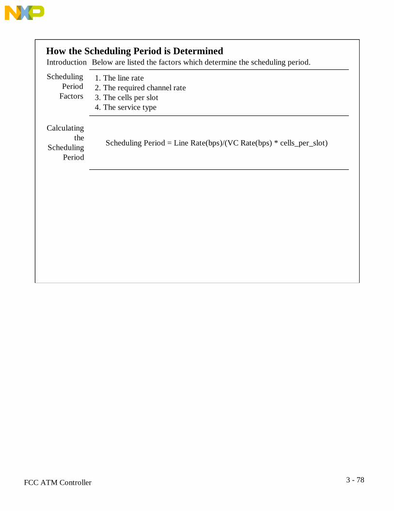
How the Scheduling Period is DeterminedIntroduction Below are listed the factors which determine the scheduling period.
SchedulingPeriod
Factors
1. The line rate2. The required channel rate3. The cells per slot4. The service type
Calculatingthe
SchedulingPeriod
Scheduling Period = Line Rate(bps)/(VC Rate(bps) * cells_per_slot)

3 - 79FCC ATM Controller
What are the Service Categories?Definition The service categories relate traffic characteristics and QoS requirements to
network behavior. Functions such as routing, CAC, and resource allocation are,in general, structured differently for each service category. Service categories aredistinguished as being either real-time or non-real-time.
ServiceTypes vs.Cell Rate
Pacing
Service TypeCBR
VBR-RTVBR-NRT
ABRUBR+UBR
Cell Rate PacingPeak cell rate
Peak and sustain cell ratePeak and sustain cell rate
Peak cell ratePeak and minimum cell rate
Peak cell rate
PriorityHighHighLowLowLowLow
• CBR: constant bit rate• VBR: variable bit rate• ABR: available bit rate• UBR: unspecified bit rate• RT: real-time• NRT: non-real-time
Acronyms
1. The table shows how the various service types can be implemented on PowerQUICC2 with the associated cell rate pacing types.2. Cell rate pacing refers to the reschedule rate in the scheduling table.3. Priority is implemented in the priority tables of the APC.
AdditionalDescription
3 - 80FCC ATM Controller
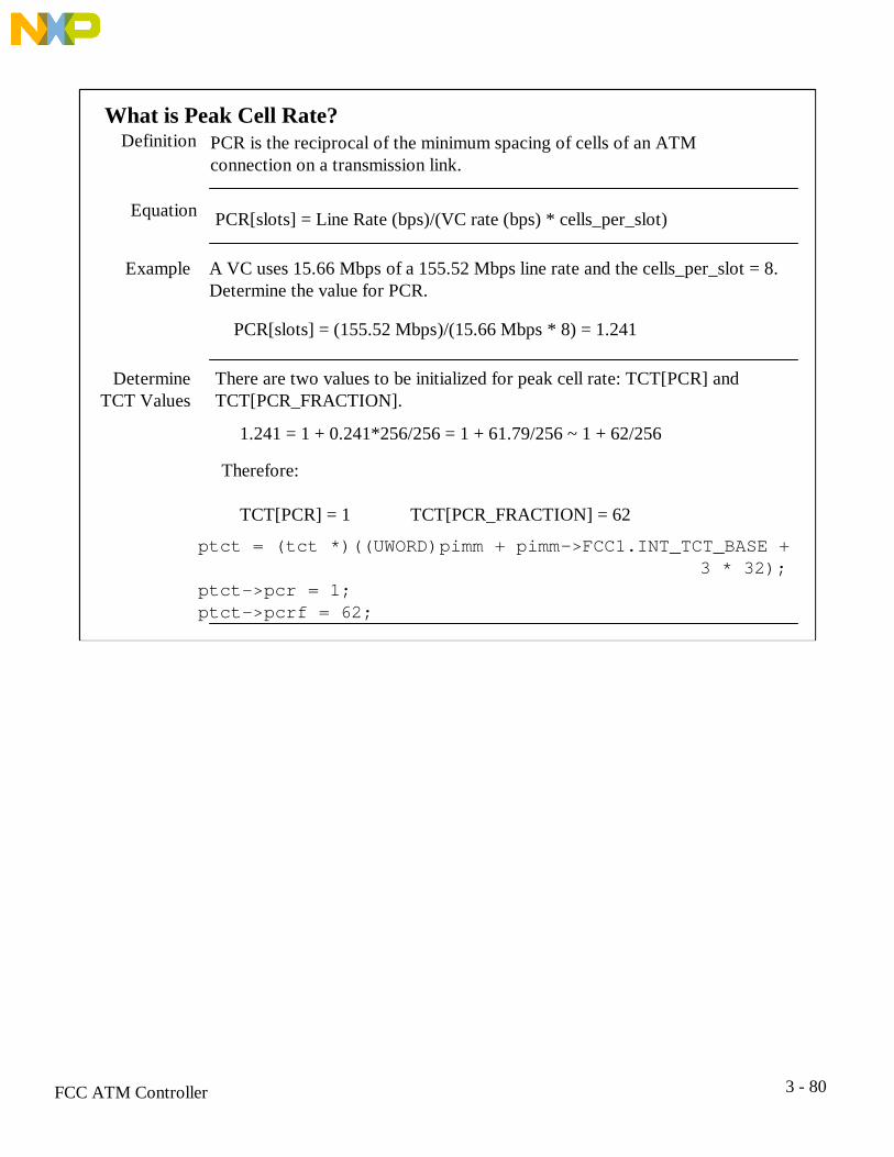
What is Peak Cell Rate?Definition
Equation
PCR is the reciprocal of the minimum spacing of cells of an ATMconnection on a transmission link.
PCR[slots] = Line Rate (bps)/(VC rate (bps) * cells_per_slot)
Example A VC uses 15.66 Mbps of a 155.52 Mbps line rate and the cells_per_slot = 8.Determine the value for PCR.
PCR[slots] = (155.52 Mbps)/(15.66 Mbps * 8) = 1.241
DetermineTCT Values
There are two values to be initialized for peak cell rate: TCT[PCR] andTCT[PCR_FRACTION].
1.241 = 1 + 0.241*256/256 = 1 + 61.79/256 ~ 1 + 62/256
Therefore:
TCT[PCR] = 1 TCT[PCR_FRACTION] = 62
ptct = (tct *)((UWORD)pimm + pimm->FCC1.INT_TCT_BASE + 3 * 32);ptct->pcr = 1;ptct->pcrf = 62;

3 - 81FCC ATM Controller
What is Peak Cell and Sustain Rate?Definition Peak cell and sustain rate is bursting at peak rate for a burst tolerance limit
followed by sustain rate outside the burst tolerance limit. Often referred to as“leaky bucket algorithm.”
Example
When there is credit for burst transmission, the APC reschedules according tothe peak rate; otherwise it reschedules according to the sustain rate.
Rescheduling
8260 PHY Switch
Initialburst Sustain Out of
buffersCreditburst
BT limitreached
Next TxBDnot ready
Next TxBDready
Credit filledActivate
• Xmit PCR • Xmit SCR • Build credits • Xmit PCR
1. When the bucket is full or nearly full, it will be filled at the sustain rate and emptiedat the sustain rate.2. At some point, because of no incoming cells, the bucket may empty. If it remainsempty for a time, it builds up credits.3. When cells become available again, they can go into the bucket at the peak rate,filling the bucket in a short time.
AdditionalDescription

3 - 82FCC ATM Controller
How to Locate the TCTE TablesIntroduction
FCC1Memory
Map
Internal Memory External Memory
DPRAM1
DPRAM2
FCC1 Parameter RAM
DPRAM3
Registers
AddressCompression
Tables
Extended Transmit Connection Tables
InterruptQueues
0x8400
Area forReceive & Transmit
BufferDescriptors
Reserved
INT_TCT_BASETransmit Connection
Tables
TCTE
TCT
INT_TCTE_BASE
EXT_TCT_BASEEXT_TCTE_BASE
The diagram below shows how the TCTE tables are located by pointers inATM parameter RAM.
1. The sustain rate and burst tolerance parameters are located in the extendedconnection tables. These are located in a way similar to the TCTs, but with theirown pointers to internal and external RAM.
Description

3 - 83FCC ATM Controller
TCTE Programming Model - VBR
TCTE - Extended Transmit Connection Table, VBR P. 29-550 1 2 3 4 5 6 7 8 9 10 11 12 13 14 15
0
2
4
SCR
8Sustain Rate (SR)
Burst Tolerance (BT)
0xA
SCR Fraction (SCRF)Sustain Rate Remainder (SRR)
0xC
0xE
Out of Buffer Rate (OOBR)
6
-
-
VBR2
Description • The TCTE programming model varies with the cell rate type. This one is for VBR.• VBR2 controls the scheduling rate according to the Cell Loss Priority value.• Out-of-buffer rate - in out of buffer state (when the transmitter tries to open TxBDwhose R bit is not set) the APC reschedules the current channel according to OOBRrate.
3 - 84FCC ATM Controller
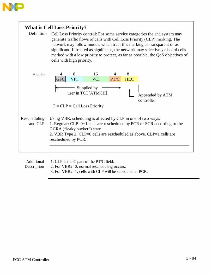
What is Cell Loss Priority?Definition
Header
Using VBR, scheduling is affected by CLP in one of two ways:1. Regular: CLP=0+1 cells are rescheduled by PCR or SCR according to theGCRA (“leaky bucket”) state.2. VBR Type 2: CLP=0 cells are rescheduled as above. CLP=1 cells arerescheduled by PCR.
Reschedulingand CLP
Cell Loss Priority control: For some service categories the end system maygenerate traffic flows of cells with Cell Loss Priority (CLP) marking. Thenetwork may follow models which treat this marking as transparent or assignificant. If treated as significant, the network may selectively discard cellsmarked with a low priority to protect, as far as possible, the QoS objectives ofcells with high priority.
GFC VPI VCI PT/C HEC4 8 16 4 8
Supplied byuser in TCT[ATMCH] Appended by ATM
controllerC = CLP = Cell Loss Priority
1. CLP is the C part of the PT/C field.2. For VBR2=0, normal rescheduling occurs.3. For VBR2=1, cells with CLP will be scheduled at PCR.
AdditionalDescription

3 - 85FCC ATM Controller
How to Initialize for Peak and Sustain RateIntroduction The diagram below shows how to calculate the peak and sustain rates.
Example Initialize channel 3 for peak and sustain with PCR = 6 Mbps, SCR = 2Mbps, MBS (maximum burst size) = 1000 cells, and cells_per_slot = 8.
PCR[slots] = Line Rate (bps)/(VC rate (bps) * cells_per_slot) = 155.52 Mbps/(6 Mbps * 8) = 3.243.24 = 3 + 0.24*256/256 = 3 + 61.44/256 ~ 3 + 62/256PCR = 3PCRF = 62
SCR[slots] = Line Rate (bps)/VC rate (bps) * cells_per_slot = (155.52 Mbps/(2 Mbps*8) = 9.729.72 = 9 + 0.72*256/256 = 9 + 184.32/256 ~ 9 + 185/256SCR = 9SCRF = 185
BT[slots] = (MBS[cells] - 2)*(SCR[slots] - PCR[slots]) + SCR[slots]= (1000 - 2)*(9.72 - 3.24) + 9.72 = 6477
1. For peak and sustain rate, three parameters must be calculated: PCR, SCR, and BT.2. Peak cell rate is calculated as shown previously.3. Sustain cell rate is calculated the same as peak except using the sustain rate.
AdditionalDescription

3 - 86FCC ATM Controller
Exercise - Initialize for Peak and Sustain Rate
ExampleProgram
ptct = (tct *)((UWORD)pimm + pimm->FCC1.____________ + 3 * 32); /* init pointer to tct */ptct->tcntrl1 |= ____; /* init for peak and sustain */ptct->pcr = 3; /* set peak cell rate to 3 */ptct->pcrf = 62; /* set fractional part to 62 */ptcte = (tcte *)((UWORD)pimm + pimm->FCC1._____________ + 3 * 32); /* init pointer to tcte */ptcte->scr = 9; /* set sustain cell rate to 9 */ptcte->scrf = 185; /* set fractional part to 185 */ptcte->bt = 6477; /* set burst tolerance to 6477*/ptcte->oobr = 20; /* set out of bufs resch to 20*/ptcte->srr = 0; /* clear sustain rate remaindr*/ptcte->vbr2 = ______; /* resch CLP=1 cells PCR */
typedef __packed__(2,2) struct { UHWORD scr; /* SUSTAIN CELL RATE */ UHWORD bt; /* BURST TOLERANCE */ UHWORD oobr; /* OUT OF BUFFRS CELL RATE*/ UBYTE srr; /* SUSTAIN RATE REMAINDER */ UBYTE scrf; /* SUSTAIN CELL RATE FRACT*/ UWORD sr; /* USED BY CP */ UHWORD vbr2; /* VBR TYPE */ UHWORD vbrresrvd[9]; /* RESERVED, MUST BE 0 */} tcte; /* TRANSMIT CONNECTION TBL*/ /* EXTENDED VBR */
AssumedStructure

3 - 87FCC ATM Controller
What is Peak and Minimum Cell Rate?Definition
Examples
If the delay in service of a priority level is greater than MDA (maximumdelay allowed) the APC starts to reschedule channels in this priority levelaccording to the MCR parameter. If the delay is less than MDA the APCwill re-schedule channels in this priority level according to PCR.
RP
SPMDA
SchedulingTable
1st case: reschedules PCR
RP
SP
MDA
SchedulingTable
2nd case: reschedules MCR
RP - SP < MDA RP - SP > MDA
1. As long as the distance between RP and SP is less than MDA time slots, channelswill be rescheduled at peak cell rate.2. When the distance exceeds MDA, channels are rescheduled at minimum cell rate.
AdditionalDescription

3 - 88FCC ATM Controller
TCTE Programming Model - UBR+
TCTE - Extended Transmit Connection Table, VBR P. 27-550 1 2 3 4 5 6 7 8 9 10 11 12 13 14 15
0
2
4
MCR
8
-
0xA
0xC
0xE
Maximum Delay Allowed (MDA)
6
-
-
MCR Fraction (MCRF)
-
-
-

3 - 89FCC ATM Controller
How to Initialize for Peak and Minimum RateIntroduction The diagram below shows how to calculate the peak and minimum rates.
Example Initialize channel 3 for peak and minimum with PCR = 7 Mbps, MCR = 1Mbps, MDA = 9, and cells_per_slot = 8.
PCR[slots] = Line Rate (bps)/(VC rate (bps) * cells_per_slot) = 155.52 Mbps/(7 Mbps * 8) = 2.782.78 = 2 + 0.78*256/256 = 2 + 199.68/256 ~ 3 + 200/256PCR = 2PCRF = 200
MCR[slots] = Line Rate (bps)/VC rate (bps) * cells_per_slot = (155.52 Mbps/(1 Mbps*8) = 19.4419.44 = 19 + 0.44*256/256 = 19 + 112.64/256 ~ 19 + 113/256MCR =19MCRF = 113
1. For peak and minimum rate, two parameters must be calculated: PCR and MCR.2. Peak cell rate is calculated as shown previously.3. Minimum cell rate is calculated the same as peak except using the minimum rate.
AdditionalDescription

3 - 90FCC ATM Controller
Example - Initialize for Peak and Minimum Rate
ExampleProgram
ptct = (tct *)((UWORD)pimm + pimm->FCC1.INT_TCT_BASE + 3 * 32); /* init pointer to tct */ptct->tcntrl1 |= 0x20; /* init for peak and minimum */ptct->pcr = 2; /* set peak cell rate to 2 */ptct->pcrf = 200; /* set fractional part to 200*/ptcte = (tcte *)((UWORD)pimm + pimm->FCC1.INT_TCTE_BASE + 3 * 32); /* init pointer to tcte */ptcte->mcr = 19; /* set minimum cell rate to 19*/ptcte->mcrf = 113; /* set fractional part to 113 */ptcte->mda = 9; /* set max delay to 9 */
typedef __packed__(2,2) struct { UHWORD mcr; /* MINIMUM CELL RATE */ UBYTE ubreservd; /* RESERVED */ UBYTE mcrf; /* MINIMUM CELL RATE FRACT*/ UHWORD mda; /* MAXIMUM DELAY ALLOWED */ UHWORD ubrresrvd[13]; /* RESERVED, MUST BE 0 */} tcte; /* TRANSMIT CONNECTION TBL*/ /* EXTENDED UBR+ */
AssumedStructure

3 - 91FCC ATM Controller
How the FCC Transmits an AAL5 Cell (1 of 3)Introduction The flow diagram below shows the AAL5 transmit operation.
FlowDiagram
Start
A PHY asserts TxClav and the FCC sends Tx request to CP
CP reads next channel number from the PHYsscheduling table
Chno > 255 CP commands DMA tofetch TCT parameters
Y
N
A
Bufferready?
YTransfer
abort
N Peak andsustain?
N
Y Rescheduleat OOBR
rate
AAL5, SOF? N
Reschedule channelY
BeforeTransmit
Starts
Host must:1. Create ATM memory structure.2. Initialize buffer descriptors.3. Write pointer of first BD into TCT.4. Issue a transmit command (this inserts the channel to the APC).
• In slave mode, TxCLAV is asserted when the FCC has a complete cell to transmit.• In master mode, TxCLAV is asserted by the PHY when it has room for a completecell.• Any of 4 TxCLAV signals might be asserted..
Assertionof TxCLAV

3 - 92FCC ATM Controller
How the FCC Transmits an AAL5 Cell (2 of 3)
FlowDiagram(cont’d)
Cell header is added
L = 1?
N
Y Add any necessarypadding and append
AAL5 trailer
Cell is sent out UTOPIA
B
A TCT[DTB]=? 0
1
60x DMA copies datafrom buffer to DPR
Local DMA copies datafrom buffer to DPR

3 - 93FCC ATM Controller
How the FCC Transmits an AAL5 Cell (3 of 3)
FlowDiagram(cont’d)
End
EOFram?
Y
N
Create interrupt queue entryY
B
TCT[AVCF] = 1?
N
Y
NDeactivate channel
A cell will be transmitted when the channel is scheduled again End
Next TxBD[R]?
1
0
TCT[IMK] = 1?
PathDescriptions
1. A channel can transmit a cell each time it is scheduled. Once a cell is transmitted,the channel must wait to be scheduled again before proceeding further.2. IMK is a bit in the TCT.3. TCT[AVCF], if set, deactivates the channel when there is no buffer ready totransmit after the end of frame.
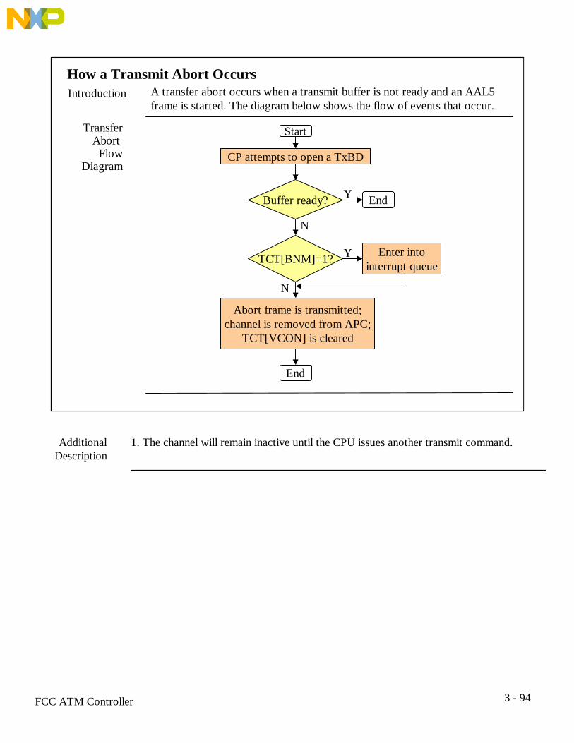
3 - 94FCC ATM Controller
How a Transmit Abort Occurs
TransferAbort
FlowDiagram
Introduction A transfer abort occurs when a transmit buffer is not ready and an AAL5frame is started. The diagram below shows the flow of events that occur.
Start
Buffer ready? Y End
N
CP attempts to open a TxBD
TCT[BNM]=1? Y Enter intointerrupt queue
N
Abort frame is transmitted;channel is removed from APC;
TCT[VCON] is cleared
End
1. The channel will remain inactive until the CPU issues another transmit command.AdditionalDescription

3 - 95FCC ATM Controller
What is an Interrupt Circular Queue?
InterruptCircular
QueueDiagram
Definition The interrupt circular queue is a structure in memory in which interruptinformation is stored when a channel interrupt occurs.
INTQ_BASEy
INTQ_PTRy
• When a channel interrupt occurs, PowerQUICC2 writes the interruptinformation to the location pointed to by INTQ_PTRy.• Entries with the valid bit set need to be processed by the CPU.• The end of the queue is marked with the W = 1.
Features
0 0 Interrupt Flags Channel Number0 0 Interrupt Flags Channel Number0 0 Interrupt Flags Channel Number1 0 Interrupt Flags Channel Number1 0 Interrupt Flags Channel Number1 0 Interrupt Flags Channel Number1 0 Interrupt Flags Channel Number0 0 Interrupt Flags Channel Number0 0 Interrupt Flags Channel Number0 0 Interrupt Flags Channel Number0 1 Interrupt Flags Channel Number
Word
CPU Pointer
V W
1. The interrupt queue is located by the pointer INTQ_BASE.2. When the CPU processes a channel interrupt, it must clear the V bit as part of theinterrupt service routine.
AdditionalDescription

3 - 96FCC ATM Controller
How to Locate the Interrupt QueuesIntroduction
FCC1Memory
Map
Internal Memory External Memory
DPRAM1
DPRAM2
FCC1 Parameter RAM
DPRAM3
Registers
InterruptQueues
0x8400 Reserved
INTT_BASE0x8466
AddressCompression
Tables
Transmit ConnectionTables
Area forReceive & Transmit
BufferDescriptors
Receive ConnectionTables
The diagram below shows the pointers used by the RISC to locate the ATMpace control tables.
Interrupt Queues Parameter Table(s)
1. INTT_BASE in parameter RAM locates the base of the Interrupt Queueparameter table(s) in dual port RAM. There can be up to four interrupt queues. Theinterrupt queue parameter table for each is located at INTT_BASE + xCT[INTQ] *16.
Description
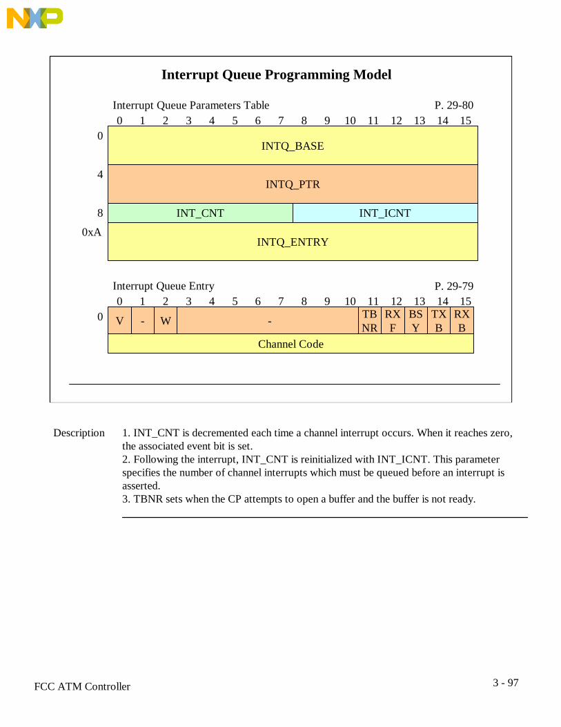
3 - 97FCC ATM Controller
Interrupt Queue Programming Model
Interrupt Queue Parameters Table P. 29-800 1 2 3 4 5 6 7 8 9 10 11 12 13 14 15
0
4
8
INTQ_BASE
INTQ_PTR
INT_CNT INT_ICNT
0xAINTQ_ENTRY
Interrupt Queue Entry P. 29-790 1 2 3 4 5 6 7 8 9 10 11 12 13 14 15
0
Channel Code
-W-V BSY
RXF
TBNR
RXB
TXB
1. INT_CNT is decremented each time a channel interrupt occurs. When it reaches zero,the associated event bit is set.2. Following the interrupt, INT_CNT is reinitialized with INT_ICNT. This parameterspecifies the number of channel interrupts which must be queued before an interrupt isasserted.3. TBNR sets when the CP attempts to open a buffer and the buffer is not ready.
Description

3 - 98FCC ATM Controller
Event Register Programming Model
FCCEx - ATM Event Register P. 29-86
0 1 2 3 4 5 6 7 8 9 10 11 12 13 14 15
- INTO2
INTO3
GINT0
INTO0
INTO1
TIRU
GRLI
GBPB
GINT3
GINT2
GINT1
FCCMx - ATM Mask Register P. 29-86
0 1 2 3 4 5 6 7 8 9 10 11 12 13 14 15
- INTO2
INTO3
GINT0
INTO0
INTO1
TIRU
GRLI
GBPB
GINT3
GINT2
GINT1
1. The event and mask registers consist of 3 groups: interrupt queue overflow, globalinterrupt, and 3 busy bits.2. There is an interrupt queue overflow and a global interrupt bit for each interrupt queue.3. TIRU is transmit internal rate underrun, GRLI is Global red-line interrupt, and GBPBis global buffer pool busy interrupt.
Description

3 - 99FCC ATM Controller
How the FCC-ATM Processes Interrupts (1 of 2)Introduction The diagram below show the flow of interrupt processing on the
PowerQUICC 2 FCC-ATM.
FCC-ATMInterrupt
ProcessingFlow
Start
Interrupt Occurs
INTQ_PTRy[V]=0?
Interrupt masked?Channel interrupt? End
NSet bit in FCCEx
End
Y Y
N
Set FCCEx.INTOy
N
EndY
Enter interrupt info into queue; set V; increment INTQ_PTRy;
decrement INT_CNTy
A
1. If a non-channel interrupt occurs, the event bit will be set directly. Examples of non-channel interrupts are: TIRU, transmit internal rate underrun; GRLI, global red-lineinterrupt; and GBPB, global buffer pool busy interrupt.2. Channel interrupts are masked in the TCT and RCT.
AdditionalComments

3 - 100FCC ATM Controller
How the FCC-ATM Processes Interrupts (2 of 2)
FCC-ATMInterrupt
ProcessingFlow
EndN
Y
Set FCCEx[GINTy];load INT_CNTy with INT_ICNTy
A
INT_CNTy0?
End
1. Each time an interrupt occurs, INT_CNT is decremented. When it is 0, the event bit isset in the FCC event register.
Description

3 - 101FCC ATM Controller
Exercise - Handling a Channel Interrupt (1 of 3)In the exercise code below, fill in the blanks to complete a routine which handles an FCC1interrupt.UWORD *ptrtbl[4]; /* CPU pntrs to intprt queues */
/* FCC1 interrupt handler */fcc1esr(){ UHWORD er; /* temp FCCE1 register */ UWORD iqe; /* temp intrpt queue entry */ UHWORD iqno; /* temp variable */ WORD *pqpt,*piq; /* q para tabl & int q pointers*/ void intoesr(); /* intrpt overflow handler */ void busyesr(); /* handler for TIRU,GRLI,GBPB */ void chesr(); /* channel interrupt handler */
er = pimm->FCCE1; /* copy event register */ pimm->FCCE1 = er; /* clear known events */ if (er & 0xF != 0) /* if interrupt overflow queue */ intoesr(er); /* go to into handler */ if (er & 0xF00 != 0) /* if tx or global busy */ busyesr(er); /* go to busy handler */
(Continued on next page)

3 - 102FCC ATM Controller
Exercise - Handling a Channel Interrupt (2 of 3)for (iqno=0; iqno<4; iqno++) /* for each of GINT bits */{ if ((er>>(iqno+4) & 1) == 1) /* if a GINT bit is 1 */ { piq = (WORD *)___________; /*init pntr to int q entry*/ do /* for each valid entry */ { iqe = *piq; /* copy intrpt queue entry*/ *piq &= __________; /* clear int que valid bit*/ chesr(iqe); /* handle channel intrpts */ if (iqe & __________ == 0) /* check if W=1 */ piq++; /* if not, increment pntr */ else /* if so, reinit pntr */ { pqpt = (UWORD *)((UWORD)pimm+pimm->FCC1._________ + iqno * __); /* init pntr to int q param tbl */ piq = *pqpt; /*init pntr to INTQ_BASE */ } } while (*piq < _); /* until an invalid entry */
(Continued on next page)
__packed__(2,2) struct immbase { /*INTRNL MEMORY MAP */ . __packed__(2,2) struct { UWORD FCC1RES[16]; /* RESERVED */ . UWORD INTT_BASE; /*INT Q TBL BASE ADDR*/ . } FCC1; .};
AssumedStructures

3 - 103FCC ATM Controller
Exercise - Handling a Channel Interrupt (3 of 3)
ptrtbl[iqno] = piq; /* update pntr table */ }}

3 - 104FCC ATM Controller
Exercise - How to Activate a Channel (1 of 2)Introduction This sheet describes how to activate a channel.
ProgrammingModel
P. 29-88COMM_INFO - in Parameter RAM0 1 2 3 4 5 6 7 8 9 10 11 12 13 14 15
- CTB PHY # ACT PRI
Channel Code
BT
P. 13-11CPCR - CPM Command Register0 1 2 3 4 5 6 7 8 9 10 11 12 13 14 15
FCC1=4,FCC2=5 0xE -RST
FLG
16 17 18 19 20 21 22 23 24 25 26 27 28 29 30 31
0xA 0xA- -
Sub-Block Code (SBC)
MCC Channel Number (MCN)Opcode

3 - 105FCC ATM Controller
Exercise - How to Activate a Channel (2 of 2)
ActivationCode
Procedure 1. Initialize channel’s TCT (including TCT[VCON=1]) and buffer descriptors.2. Initialize COMM_INFO in parameter RAM3. Write the transmit command to the command register.
Write the code to activate channel 300 on PHY 2 for CBR and AAL5.Connection tables are on the local bus.pimm->FCC1.comm_info.chdata = _____;pimm->FCC1.comm_info.chcode = 300;pimm->CPCR = __________;
__packed__(2,2) struct immbase { /*INTRNL MEMORY MAP */ . __packed__(2,2) struct { UWORD FCC1RES[16]; /* RESERVED */ . __packed__(2,2) struct { UHWORD chdata; /*CTB,PHY#,ACT,PRI */ UHWORD chcode; /* CHANNEL NUMBER */ UHWORD bt; /* BURST TOLERANCE */ } comm_info; /* ATM XMIT COMMAND INFO */ . } FCC1; .};
AssumedStructures

3 - 106FCC ATM Controller
What is the UTOPIA Interface?Definition The universal test and operations PHY interface for ATM (UTOPIA)
defines the interface between the 8260 and the PHY
MPC8260
TxData[15-0]/[7-0]TxSOCTxEnb*TxPrtyTxClk
TxClav[0-3]TxAddr[0-4]
RxData[15-0]/[7-0]RxSOCRxEnb*RxPrtyRxClk
RxClav[0-3]RxAddr[0-4]
Master
MPC8260
TxData[15-0]/[7-0]TxSOCTxEnb*TxPrtyTxClk
TxClavTxAddr[0-4]
RxData[15-0]/[7-0]RxSOCRxEnb*RxPrtyRxClk
RxClavRxAddr[0-4]
Slave
Pinouts
1. Data transfers are done using the data, SOC, Enb, and Prty pins (and also theclock).2. Address polling is done using the Clav and Addr pins.3. Two types of UTOPIA address polling are supported by MPC8260: - Multiplexed - Direct4. Data transfers and address polling can be done concurrently.
UTOPIASummary

3 - 107FCC ATM Controller
What is Multiplexed Polling?Definition In UTOPIA level 2, one MPHY port is selected for a cell transfer while
other MPHY ports are polled for TxClav or RxClav status.
ExamplePowerQUICC 2
TxC
lav[
0]
RxC
lav[
0]
PHY 0 PHY 1 PHY 29 PHY 30Tx
Add
r[0-
4]
RxA
ddr[
0-4]
RxC
lk
TxC
lk
Dat
aC
onne
ctio
ns
• Up to 31 PHY devices can be connected; 0x1F is the NULL PHY.• An address is asserted every other clock. On the next clock, the addressedPHY asserts or negates TxClav or RxClav to indicate it is ready for transmitor receive data.• Data can be transferred on the data lines while polling occurs.
Features
1. Receive polling and transmit polling occur at the same time.2. On the clocks during which a PHY is asserting or negating TxClav or RxClav, theaddress on the address lines is 0x1F.
AdditionalDescription

3 - 108FCC ATM Controller
How the Multiplexed Polling Mode Transmits DataIntroduction The diagram below shows a polling phase followed by a selection phase.
TimingDiagram
1 2 3 4 5 6 7 8 9 10 11 12 13 14 15 16 17 18 19 20TxClk
TxAddr
TxClav
TxEnb*
35 36 37 38 39 40 41 42 43 44 45 46 47 48 1 2 3 4TxData
TxSOC
Cell transmission to PHY #N PHY #29
0x1F #25 #26 #27 #29RR: #30FP: #0#28
Polling Polling1
2
3
4
5
6 7
Description 1. Completion of transmitting a cell to PHY N occurs at time 15.2. During the next clock cycle, PHY #29 is asserted on TxAddr to indicate this is thenext PHY to transmit to.3. Start of cell transmit to PHY #29 begins with time16.4. While a cell is being transmitted, the master is asserting addresses on TxAddr. Inthis diagram, an address to be polled is asserted every other clock cycle.5. In between poll addresses, the null address, 0x1F, is asserted.6. Following the assertion of a poll address in a particular clock cycle, TxClav isasserted or negated in the next clock cycle to indicate if the associated PHY has roomfor another cell or not.7. At time 9, address #29 is asserted and at time 10, the TxClav indicates there isroom in the PHY #29 FIFO for another transmit cell. TxAddr and TxClav remainasserted until the transmit for PHY #29 begins.
Following 2, polling begins again. If the polling mode is Round Robin, #30 is pollednext. If Fixed Priority, #0 is polled next. At the same time, transmit of data begins for#29 with the header octets.

3 - 109FCC ATM Controller
What is Direct Status Indication?Definition For each PHY port, the status signals RxClav and TxClav are permanently
available according to UTOPIA 1 level specification.
ExamplePowerQUICC 2
TxC
lav[
0]
PHY 0 PHY 1 PHY 2 PHY 3
All
Oth
erC
onne
ctio
ns
• When a PHY has a receive cell to transfer or has room for a transmit cell, itasserts RxClav or TxClav respectively.• No addresses required for polling, but required for data transfer.
Features
RxC
lav[
0]
TxC
lav[
1]R
xCla
v[1]
TxC
lav[
2]R
xCla
v[2]
TxC
lav[
3]R
xCla
v[3]
TxA
ddr[
0-1]
RxA
ddr[
0-1]
1. Up to four PHYs max can be connected.2. In this mode, three pins that would normally be for addresses are used for cellavailable signals:
AdditionalDescription
This pin... ..becomes this function...TxAddr[2] TxClav[1]TxAddr[3] TxClav[2]TxAddr[4] TxClav[3]RxAddr[2] RxClav[1]RxAddr[3] RxClav[2]RxAddr[4] RxClav[3]

3 - 110FCC ATM Controller
How the Direct Status Indication Mode Receives DataIntroduction The diagram below shows direct status indication for receiving data.
TimingDiagram 1 2 3 4 5 6 57 58 59 60
111
RxClk
RxAddr
RxClav0
RxEnb*
H1 48 H1 48 H1 H2RxData[7:0]
RxSOC
112
113
114
164
165
166
167
0 X 2X X X X
RxClav1
RxClav2
RxClav3
48
Cell transfer(port #0)
Cell transfer(port #2)
Cell transfer(port #2)
2
3
4
5
6
7
8
910
11
12
1
1. In this diagram, polling of the PHYs begins while no cell is being transferred.2. At clock edge #3, the MPC8260 detects that PHY #0 has a cell available becauseRxClav is asserted.3. The 8260 then asserts address 0 on the address lines.4. PHY #0 detects its address on clock edge #4.5. PHY #0 detects Receive Enable asserted on edge #5.6. Also at edge #5, the 8260 detects that port #2 has a cell available.7. At edge #57, near the end of the PHY #0 cell transfer, the MPC8260 assertsaddress 2 on the address pins.8. PHY #0 and #2 detect the new address9. At edge #59, PHY #2 detects RxEnb asserted and starts the cell transfer.10. At edge #111, no PHY has indicated another cell available. RxEnb remainsasserted and the MPC8260 detects that PHY #2 has another cell available on edge#113.11. At clock edge #164, again no cell is available from PHY #0, #1, or #3.12. At clock edge #166, it detects no cell available from PHY #2, so the 8260deasserts RxEnb*
Description

3 - 111FCC ATM Controller
FPSMR Programming Model
FPSMRx - FCCx Protocol Specific Mode Register P. 29-84
0 1 2 3 4 5 6 7 8 9 10 11 12 13 14 15
LAST PHY/PHY IDICD TUMS
RUMS
- HECI
RUMP
UPLM -RX
PTUMP - TSI
ZERSIZE
UPRM
TEHS REHS
16 17 18 19 20 21 22 23 24 25 26 27 28 29 30 31TUDC
RUDC
UDC Mode Parameters UTOPIA Parameters

3 - 112FCC ATM Controller
PM5350
How to Interface the MPC8260 to a PHY, Management InterfaceIntroduction The diagram below shows the management interface of MPC8260 to a
PMC-Sierra PHY.
ConnectionDiagram
MPC8260
A[24-31]
BCTL0*PWE0*/PDQM/PBS0*
DP6/CSE0/IRQ6*
A[7-0]D[0-7] D[7-0]
CS*
WR*RD*
RST*ALEINT*
The management interface exists for reading and writing of control andstatus information. For example, an address is assigned to the PHY using themanagement interface.
ATMCS0*
ATMRST*
Purpose
1. Data is transferred over an 8-bit data bus.2. The PHY device is selected with the ATMCS0* signal from a Mach221.3. A register within the PHY is selected with the 8 address lines.4. The PHY is read enabled by BCTL0*, a 60x bus buffer control signal that operatesaccording to SIUMCR[BCTLC].5. The PHY is write enabled by PWE0*.6. The PHY device is reset with the ATMRST* signal from a Mach221.7. The PHY INT* pin is asserted to indicate an alarm or other event has occurred.
PinFucntions

3 - 113FCC ATM Controller
How to Allocate the FCC Master UTOPIA Address Pins (1 of 2)
Introduction
Allocatingthe Pins
Two UTOPIA address pins are shareable between FCC1 and FCC2 allowingthe user to configure for the number of PHYs desired for each FCCx.
RxADDR[0]/PC14
RxADDR[2]/PC6
1:RxADDR[3]
RxADDR[1]/PC12
RxADDR[2]/PA5RxADDR[1]/PA4
MPC8260
2:RxADDR[4]/PD29
1:RxADDR[4]2:RxADDR[3]
/PD18
RxADDR[0]/PA3
FCC1
FCC2
MAD4=1
MAD4=0
MAD3=1
MAD3=0
1. Coming up from reset and after configuring the port registers, PC12 is RxADDR[0]for FCC2 and PC14 is RxADDR[1] for FCC2. This gives FCC2 5 address pins andFCC1, 3 address pins: RxADDR[2-4].2. To reconfigure either of these pins for FCC1, CMXUAR[MAD0] and/orCMXUAR[MAD1] must be set.
Comments

3 - 114FCC ATM Controller
How to Allocate the FCC Master UTOPIA Address Pins (2 of 2)
Example After first initializing the port pins as determined by the PIN-MUXapplication, program the MPC8260 UTOPIA interface so that FCC1 andFCC2 can each interface to 15 PHYs.
pimm->CMXUAR |= 1<<(15-6); /* set MAD4 */
CMXUAR - UTOPIA Address Register P. 15-7
0 1 2 3 4 5 6 7 8 9 10 11 12 13 14 15
F2IRB -- MAD4
MAD3 F1IRBSA
D0SAD1
SAD2
SAD3
SAD4
ProgramModel
PossibleConfigurations
FCC1 FCC2
31 7
15 15
7 31
No. ofPHYs
MAD4 MAD3
1 1
1 0
0 0
1. The three possible configurations and the required values for MAD0 and 1 areshown here.2. These configurations are controlled in the CMXUAR.3. Notice this registers also has 5 bits, SAD[0-4], for controlling the pins in slavemode.
Comments
__packed__(2,2) struct immbase { /*INTRNL MEMORY MAP */ . UHWORD CMXUAR; /*UTOPIA ADDRESS REGISTER */ .};
AssumedStructures

3 - 115FCC ATM Controller
How to Allocate the FCC Slave UTOPIA Address Pins
Introduction
Allocatingthe Pins
Five UTOPIA address pins are shareable between FCC1 and FCC2 allowingthe user to configure for the number of PHYs desired for each FCCx.
1:RxADDR[4]
MPC8260
FCC1
FCC2
2:RxADDR[0] /PD18
1:RxADDR[3]2:RxADDR[1] /PD29
1:RxADDR[2]2:RxADDR[2] /PC6
1:RxADDR[1]2:RxADDR[3] /PC12
1:RxADDR[0]2:RxADDR[4] /PC14
1. In slave mode, these 5 pins can be allocated to either FCC1 or FCC2.2. If SADx=1, the pin is connected to FCC1; otherwise to FCC2.
Comments

3 - 116FCC ATM Controller
How to Initialize for UTOPIA (1 of 2)Introduction The diagram below shows the procedure to initialize for UTOPIA.
Procedure Step Action
2
Initialize CMXUARMAD[0-1]:master addr pinsSAD[0-4]:slave addr pins
(15-7)
3
Run the PIN_MUX application and program the Port regs as shown.
1
Initialize CMXFCRFC1: FCC1 connectionRF1CS: FCC1 recv clock sourceTF1CS: FCC1 xmit clock sourceFC2: FCC2 connectionRF2CS: FCC2 recv clock sourceTF2CS: FCC2 xmit clock source
(15-12)

3 - 117FCC ATM Controller
How to Initialize for UTOPIA (2 of 2)
Procedure(cont’d)
Step ActionInitialize FPSMR for UTOPIA parameters
TUMS:transmit master/slaveRUMS:receive master/slaveLAST PHY/PHY ID:number/addressRxP:check receive parity TUMP:transmit single/multiple PHYTSIZE:transmit data bus sizeRSIZE:receive data bus sizeUPRM:round robin/fixed priorityUPLM:multiplex/direct modeRUMP:receive single/multiple PHY
(29-84)
4

3 - 118FCC ATM Controller
Exercise - UTOPIA ConfigurationProblem Configure FCC1 to operate with the following: 1) 8-bit master, 2) direct
polling (4 PHYs), and 3) fixed priority. Configuration is for both receive andtransmit. The receive clock is CLK9 and the transmit clock, CLK11.
Program pimm->CMXFCR = __________; /*connect clocks *//* Port registers are zero from reset */pimm->PSORC = 0x030f0000; /* init port registers*/pimm->PSORD = 0x01000004;pimm->PDIRA = 0x00003fcd;pimm->PDIRC = 0x030f0000;pimm->PDIRD = 0x0100b004;pimm->PPARA = 0x003fffff;pimm->PPARB = 0x00000000;pimm->PPARC = 0x030f0000;pimm->PPARD = 0x0100f004;pimm->CMXUAR |= _________; /*enbl FCC1 mastr pins*/pimm->FPSMR1 = _______; /* enable UTOPIA modes*/
__packed__(2,2) struct immbase { /*INTRNL MEMORY MAP */ . UWORD FPSMR1; /* FCC1 PROTOCOL SPEC MODE */ . UWORD CMXFCR; /* FCC CLOCK ROUTE REG */ . UHWORD CMXUAR; /*UTOPIA ADDRESS REGISTER */ .};
AssumedStructures

3 - 119FCC ATM Controller
What is the Transmit Internal Rate Mode?Definition A PHY can be programmed to transmit data at the rate of an internal clock
rather than the TxClav rate.
LogicalRepresentation,
InternalRate
ModeBaudRateGen
PHY #0 Divider
PHY #1 Divider
PHY #2 Divider
PHY #3 Divider
DFF
TxClav,PHY #0
TxEnb*Clock
FTIRRx - FCCx Transmit Internal Rate Register P. 27-860 1 2 3 4 5 6 7
PHY #0 DividerTRM
ProgrammingModel 8 9 10 11 12 13 14 15
PHY #1 DividerTRM
16 17 18 19 20 21 22 23
PHY #2 DividerTRM
24 25 26 27 28 29 30 31
PHY #3 DividerTRM
1. The Transmit Internal Rate Mode allows the 8260 to set the transmit rate for 4PHYs on each FCC.2. The internal rate is set using a baudrate generator as a common clock sourcewhich drives a divider for each PHY.3. Each time the PHY internal clock occurs, TxEnb* is asserted if TxClav wasasserted previously. If the PHY asserts TxClav and if there is no response becausethe PHY divider has not timed out, then the PHY transmits an idle cell.4. The programming model is a 32-bit register for each FCC. Each register isdivided into 4 bytes, each PHY rate controlled by a byte.
Description

3 - 120FCC ATM Controller
How to Initialize the Transmit Internal Rate ModeIntroduction This diagram shows the procedure to initialize for Transmit Internal Rate Mode.
Procedure 1. Calculate the required BRG Clock divider value.2. Calculate the divider value required for each PHY. 3. Initialize BRG 5, 6, 7, or 8.4. Connect BRG to FCC. 5. Initialize the FTIRR.
Example FCC1 is connected to four 155 Mbps PHY devices and the maximumtransmission rate is 155 Mbps for the first PHY and 10 Mbps for the rest ofthe PHYs. The CPM clock is 133 MHz.
CD = (53 * 8) * ClkFreq * PHYRatePeriod = (53 * 8) * 133/2 * 106 * (1/155.52) * 10-6
= 181
FTIRR0 divider = 1FTIRR1,2,3 dividers = 15
pimm->BRGC7 = 0x10000 | 181<<1; /* init BRG7 */pimm->CMXUAR |= 0x80; /* connect BRG7 to FCC1 */pimm->FTIRR1 = 0x808E8E8E; /* enable internal */ /* rate mode & dividers */
__packed__(2,2) struct immbase { /*INTRNL MEMORY MAP */ . UWORD FTIRR1; /* FCC1 XMIT INTRNL RATE */ . UWORD BRGC7; /* BRGC7 CONFIG REG */ . UHWORD CMXUAR; /*UTOPIA ADDRESS REGISTER */ .};
AssumedStructures

3 - 121FCC ATM Controller
What is AAL0 Protocol?Definition An AAL0 cell is the same as AAL5 except: 1) the header is stored or
obtained from the buffer, and 2) it is stand-alone, i. e. there are no frames.
FCCxH
AddressMappingProcess
ReceiveFlow
Diagram
ConnectionTable BD Arrays
Buffers
52 bytes of data
CellHeader
FCCxH
TransmitFlow
Diagram
ConnectionTable
BD Arrays
Buffers
52 bytes of data
ATMPace
ControlTxClav
CellHeader
1. A buffer contains one AAL0 cell.2. On transmit, the cell header can optionally be taken from the buffer or the TCT.
Comments

3 - 122FCC ATM Controller
How the FCC Receives an AAL0 Cell (1 of 2)Introduction The flow diagram below shows the AAL0 receive operation.
FlowDiagram
Start
A
A PHY asserts RxClav, UTOPIA I/F asserts RxEnb, and a complete cell is read into the FIFO
CP reads cell header and performs lookup, AC or CAM
Matchfound?
N Cell is discarded;UNI statistics tables
are updated End
Y
Chno > 255 CP commands DMA tofetch RCT parameters
Y
N
Specialcell?
N
Y
Channel number =1,the raw cell queue
Management cells and filtered cells (special OAM cells) are sent to channel1 aka the raw cell queue.
SpecialCells
BeforeReceive
Starts
Host must:1. Create ATM memory structure.2. Initialize buffer descriptors.3. Write pointer of first BD into RCT.
• In slave mode, RxCLAV is asserted when the FCC can receive a complete cell.• In master mode, RxCLAV is asserted by the PHY when it has a complete cell topass on to the FCC.• Any of 4 RxCLAV signals might be asserted, for up to 4 PHYs.
Assertionof RxCLAV

3 - 123FCC ATM Controller
How the FCC Receives an AAL0 Cell (2 of 2)
FlowDiagram(cont’d)
A
Recvbuffer empty
?
Y
N
Receiver goesto hunt mode
End
BTM copies cell to RCELL_TMP_BASE
RCT[DTB]=? 0
60x DMA copies datafrom DPR to buffer
1
Local DMA copies data from DPR to buffer
Recvbuffer empty
?
Y
Set appropriate status bits in RxBD
End
N
• For AAL0 cells, a CRC10 calculation is performed and the OAM bit is setaccording to the result..
RxBD StatusBits

3 - 124FCC ATM Controller
What is the Receive Raw Cell Queue?Definition The receive raw cell queue is used for removing management cells from
the regular cells flow to the host.
FCCxH
AddressMappingProcess
FlowDiagram
CT1
BD Arrays
Buffers
52 bytes of data
CellHeader
ConnectionTable
OAM, RM, or VCI cell
Conditions 1. OAM F5 segment filtering: PTI = 0b100 and RCT[SEGF] = 1.2. OAM F5 end-to-end filtering: PTI = 0b101 and RCT[ENDF] = 1.3. RM cell filtering: PTI = 0b110 and ABR not enabled.4. Reserved PTI value: PTI = 0b1115. VCI filtering: set bit(s) in VCIF parameter RAM
• Channel 1 must be configured as AAL0
1. When a cell comes in, it is first checked for a match, either by address compressionor CAM.2. If there is no match the cell is discarded.3. If there is a match, the header is checked for the conditions listed above.4. If one of those conditions is true, the cell goes to the receive raw cell queue,otherwise it goes to the associated VC buffer.
Flow ofEvents

3 - 125FCC ATM Controller
How the FCC Transmits an AAL0 Cell (1 of 3)Introduction The flow diagram below shows the AAL0 transmit operation.
FlowDiagram
Start
Chno > 255 CP commands DMA tofetch TCT parameters
Y
N
A
Bufferready?
Y
Transfer abortN
A PHY asserts TxClav and the FCC sends Tx request to CP
CP reads next channel number from the PHYsscheduling table
BeforeTransmit
Starts
Host must:1. Create ATM memory structure.2. Initialize buffer descriptors.3. Write pointer of first BD into TCT.4. Issue a transmit command (this inserts the channel to the APC).
• In slave mode, TxCLAV is asserted when the FCC has a complete cell to transmit.• In master mode, TxCLAV is asserted by the PHY has room for a complete cell.• Any of 4 TxCLAV signals might be asserted.
Assertionof TxCLAV
1. If a channel is to be transmitted, and it has no buffer ready, transfer abort occurs.Comment

3 - 126FCC ATM Controller
How the FCC Transmits an AAL0 Cell (2 of 3)
FlowDiagram(cont’d)
A TCT[ACHC]=?
0
1
TCT[DTB]=? 0
1
Local DMA copies
buffer to DPR
28 bits is obtained from TCT for hdr
60x DMA copies
buffer to DPR
Cell is sent out UTOPIA
TCT[CR10]?
0
1 Append CRC10
B
1. TCT[ACHC] controls from where the header will be obtained, either the TCT or thebuffer.
Comment

3 - 127FCC ATM Controller
How the FCC Transmits an AAL0 Cell (3 of 3)
FlowDiagram(cont’d)
IMK? Create interrupt queue entry1
B
0
End
TCT[AVCF] ? 1
0Deactivate channel
Next TxBD[R]?
1
0
PathDescriptions
1. IMK is the interrupt mask bit in the TCT.2. TCT[AVCF], if set, deactivates the channel when next buffer is not ready.

3 - 128FCC ATM Controller
AAL0 Specific Connection Table Programming Model (1 of 2)
AAL0 Specific - Receive Connection Table P. 29-490 1 2 3 4 5 6 7 8 9 10 11 12 13 14 15
-0xE
- RXBM
-
0x10
0x14
0x16
0x18 -
INVE10-
INVE - inverted empty bit.RXBM - receive buffer interrupt mask
Description This part of the RCT is specific to an AAL0 frame.1. RXBM determines if the receive buffer event is sent to the interrupt queue or not.2. INVE determines if the Empty bit in the RxBD is to be given an invertedinterpretation. Useful with ATM-TDM bridging mode.
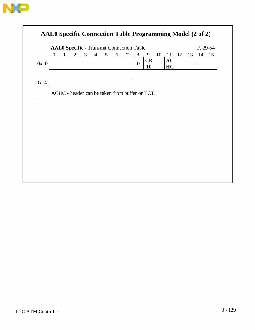
3 - 129FCC ATM Controller
AAL0 Specific Connection Table Programming Model (2 of 2)
0x10
-0x14
AAL0 Specific - Transmit Connection Table P. 29-540 1 2 3 4 5 6 7 8 9 10 11 12 13 14 15
--CR100- AC
HC
ACHC - header can be taken from buffer or TCT.
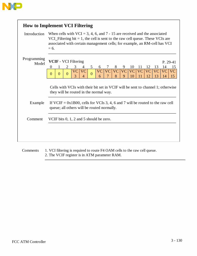
3 - 130FCC ATM Controller
How to Implement VCI Filtering
Introduction
ProgrammingModel
When cells with VCI = 3, 4, 6, and 7 - 15 are received and the associatedVCI_Filtering bit = 1, the cell is sent to the raw cell queue. These VCIs areassociated with certain management cells; for example, an RM-cell has VCI= 6.
0 VC6
VC7
VC9
VC10
VC11
VC12
VC13
VC14
VCIF - VCI Filtering P. 29-410 15
0 VC8
1 2 3 4 5 6 7 8 9 10 11 12 13 14
0 0 VC3
VC4
VC15
Cells with VCIs with their bit set in VCIF will be sent to channel 1; otherwisethey will be routed in the normal way.
Example If VCIF = 0x1B00, cells for VCIs 3, 4, 6 and 7 will be routed to the raw cellqueue; all others will be routed normally.
Comment VCIF bits 0, 1, 2 and 5 should be zero.
1. VCI filtering is required to route F4 OAM cells to the raw cell queue.2. The VCIF register is in ATM parameter RAM.
Comments

3 - 131FCC ATM Controller
What is an OAM Cell?Definition An OAM (Operation, Administration, and Maintenance) cell is used to
provide network fault indication, performance information, and data anddiagnosis functions.
OAM CellStructure ATM
Header
5 1
CRC-10
2
Data specific to OAM type
45
Identifies OAM cell type (4 bits) and function type (4 bits)Example: cell type=1 and function type=4 is faultmanagement continuity check.
Normal header except use specified as follows:
End-to-end OAM F5 flow cell
Segment OAM F5 flow cell
End-to-end OAM F4 flow cell
Segment OAM F4 flow cell
Use VC
3
4
a
a
PTI
0a0
0a0
4
5a = available for use by the appropriate ATM layer function
1. The 2-byte field labeled CR10 is really 10 bits of CRC plus 6 reserved bits.

3 - 132FCC ATM Controller
How an F4 Cell is Received
Introduction
ReceiveFlow
Diagram
An F4 cell is an AAL0 cell directed either to its VCI buffer or, if enabled inthe VCIF, to the raw cell queue.
Start
F4 cell is received
VCI=?3 4
VCIF[3]=? VCIF[4]=?Route tochnum
0 Route tochnum
0
Route tochannel 1
1 1
End
Address match?
Y
Discardcell
End
N
End End
1. Before an F4 cell (or any other cell for that matter) can be directed, there must be anaddress match.2. If the FCC is implemented on a network, F4 would normally be routed to the rawcell queue. If not, the user might prefer to route them to their actual channel numbers.
Comments

3 - 133FCC ATM Controller
Exercise - Transmit OAM Cells Multi-PHY (1 of 2)In the exercise code below, fill in the blanks to complete a transmit an OAM cell tomultiple PHYs on FCC2./* Transmit an OAM cell to multiple PHYs */xmitoam(n1,n2)UHWORD n1,n2; /* first and last PHY numbers */{ struct descs { /* xmit buffer desc 0 */ txbdfa TxBD0; }; struct descs *pdsc; /* pointer to BD */
ptct = (tct *)((UWORD)pimm + pimm->FCC2.INT_TCT_BASE + __); /* init tct pntr to tct1 */ pimm->FCC2.comm_info.chcode = _; /* assign channel */ ptct->tcntrl1 |= _; /* set VCON,AVCF already set */ pdsc = (descs *) (pimm->FCC2.BD_BASE_EXT + (ptct->tcntrl3) & 0x00FFFFF0); /* init pntr to descriptr*/ pdsc->TxBD0.txbdsac |= 0xA000; /* make BD ready */
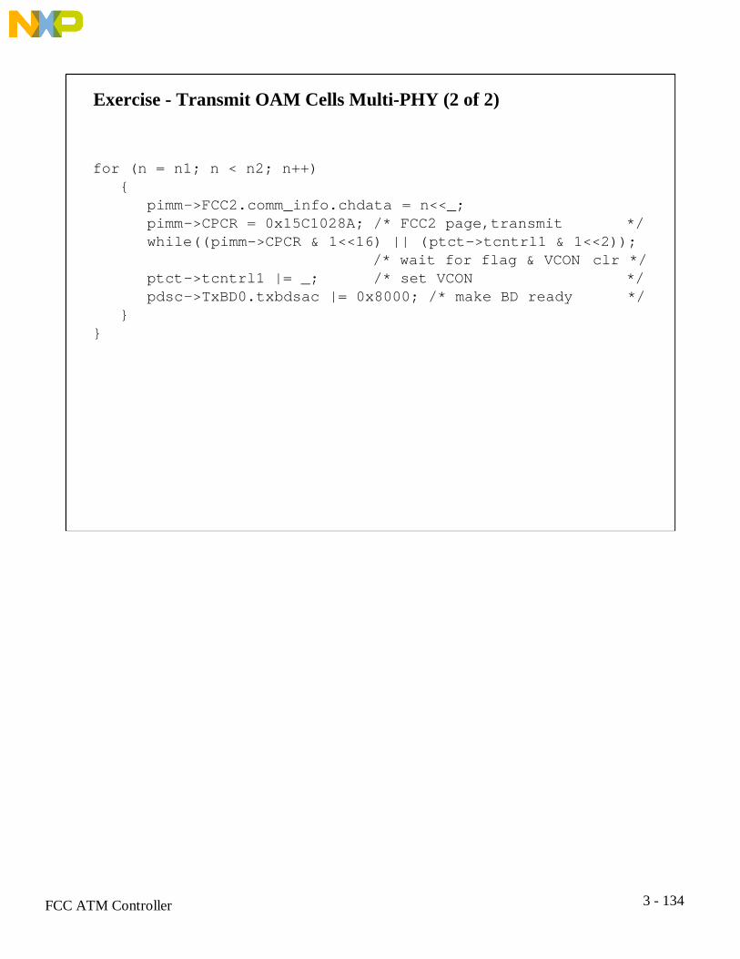
3 - 134FCC ATM Controller
Exercise - Transmit OAM Cells Multi-PHY (2 of 2)
for (n = n1; n < n2; n++) { pimm->FCC2.comm_info.chdata = n<<_; pimm->CPCR = 0x15C1028A; /* FCC2 page,transmit */ while((pimm->CPCR & 1<<16) || (ptct->tcntrl1 & 1<<2)); /* wait for flag & VCON clr */ ptct->tcntrl1 |= _; /* set VCON */ pdsc->TxBD0.txbdsac |= 0x8000; /* make BD ready */ }}

3 - 135FCC ATM Controller
How an F5 Cell is Received
Introduction
ReceiveFlow
Diagram
An F5 cell is an AAL0 cell directed either to its VCI buffer or, if enabled inthe VCIF, to the raw cell queue.
Start
F5 cell is received
PTI=?4 5
RCT[SEGF]=? RCT[ENDF]=?Route tomatchedchannel
0 Route tomatchedchannel
0
Route tochannel 1
1 1
End
Address match?
Y
Discardcell
End
N
End End
1. Before an F5 cell (or any other cell for that matter) can be directed, there must be anaddress match.2. If the FCC is implemented on a network, F5 would normally be routed to the rawcell queue. If not, the user might prefer to route them to their actual channel numbers.
Comments

3 - 136FCC ATM Controller
What is ATM-to-TDM Interworking?Definition ATM-toTDM Interworking is a special mode that enables automatic
bridging between AAL1/AAL0 to transparent mode over a TDM interface.
Example
This mode is useful for: 1) Circuit emulation service (CES), 2) Carryingvoice over ATM, and 3) multiplexing several low speed services voice anddata onto one ATM connection.
Applications
ATMTx
MCCRx
UTOPIAInterface
TDMInterface
BDRing Buffer 1
Buffer 2
Buffer 3
1. In this example, the MCC is using the BD ring as RxBDs. The ATM is using thesame ring as TxBDs.2. The MCC must be receiving data ahead of the ATM buffer pointer.3. In order for this to work, the ATM and MCC must be programmed for theopposite E bit polarity.
TheOperation

3 - 137FCC ATM Controller
What is AAL1 Protocol?Definition The AAL1 protocol is CBR and requires a timing relationship between
source and destination.
FCCxH
AddressMappingProcess
ReceiveFlow
Diagram
ConnectionTable BD Arrays
Buffers
46 or 47 bytes of data
CellHeader
FCCxH
TransmitFlow
Diagram
ConnectionTable
BD Arrays
Buffers
48 bytes of data
ATMPace
ControlTxClav
CellHeader
1. One byte of the receive cell is a sequence number2. Optionally, another byte can be used as a pointer for partially filled cells which canresult for increased performance.
Add’lComments

3 - 138FCC ATM Controller
What is an AAL1 Cell?Definition An AAL1 cell is a basic ATM cell consisting of a 46 or 47-octet AAL PDU
(Protocol Data Unit), a sequence octet, optionally a pointer octet for partiallyfilled cells, and a 5 octet cell header.
ExampleCell
Header PDU or payload
46 or 47 octets
53 octets
GFC VPI VCI PT/C HEC4 8 16 4 8
Supplied byuser in TCT[ATMCH] Appended by ATM
controller
SN4
SNP4
Pointer8
1. The AAL1 cell is like the AAL5 cell except that it uses 1 byte of the payload for asequence number and , optionally, another byte for a pointer.2. SN is a sequence number. It is used for detection of mistakenly inserted cells or lostcells.3. SNP is an error detection field for SN.4. The pointer is used for partially filled cells.
CellDescription

3 - 139FCC ATM Controller
What is an RM Cell?Definition An RM (Resource Management) cell is used to control the cell flow of ABR
(Available Bit Rate) connections.
RM CellStructure ATM
Header
5
ID
1Sta
1
ER CCR
2 2
MCR
2
QL
4
SN
4
CRC-10
2
Reserved
30
• ID: protocol identifier• Sta: direction(DIR), BECN cell(BN), congestion indication(CI), noincrease(NI), request/acknowledge(RA).• ER: explicit cell rate• CCR: current cell rate• MCR: minimum cell rate• QL: queue length• SN: sequence number

3 - 140FCC ATM Controller
What is ABR-AAL5 Flow Control?Definition ABR flow control occurs between a sending end-system and a receiving
end-system for feedback rate adaption.
FlowDiagram
Source
EndSystem
Desti-nation
EndSystemNetwork
ElementNetworkElement
NetworkElement
• For source-to-destination information flow, there is a control loopconsisting of two RM-cell flows, one forward and one backward.• A network element may
- Directly insert feedback control information into RM-cell- Generate backward RM-cells- Indirectly inform the source about congestion
Forward information flow
RM-cell flow
1. A source generates forward RM-cells which are turned around by the destination andsent back to the source as backward RM-cells.2. These backward RM-cells carry feedback information provided by the network elementsand/or the destination.
GeneralFlow

3 - 141FCC ATM Controller
How the FCC Transmits an AAL1 Cell (1 of 2)Introduction The flow diagram below shows the operation to transmit an AAL1 cell.
FlowDiagram
Start
47 bytes are obtained from buffer
Bufferready?
Y
Transfer abort
A
Structuredformat?
Y
N46 or 47 bytes are
obtained from buffer
Header (SN and SNP) is generated and inserted
Header (SN, SNP andstructured pointer) is generated and inserted
Cell is sent out UTOPIA
1. If a channel is to be transmitted, and it has no buffer ready, transfer abort occurs.2. If the amount of data in the buffer is such that a cell is only partially filled, paddingwill automatically occur.
Comments

3 - 142FCC ATM Controller
How the FCC Transmits an AAL1 Cell (2 of 2)
FlowDiagram(cont’d)
End
Create interrupt queue entryY
TCT[AVCF] = 1?
N
Y
NDeactivate channel
Next TxBD[R]?
1
0
TCT[IMK] = 1?
A
PathDescriptions
1. A channel can transmit a cell each time it is scheduled. Once a cell is transmitted,the channel must wait to be scheduled again before proceeding further.2. IMK is a bit in the TCT.3. TCT[AVCF], if set, deactivates the channel when there is no buffer ready totransmit after the end of frame.