Embed Size (px)
Citation preview
FAx86: An Open-Source FPGA-Accelerated x86Full-System Emulator
by
Elias El Ferezli
A thesis submitted in conformity with the requirementsfor the degree of Master of Applied Science (M.A.Sc.)
Graduate Department of Electrical and Computer EngineeringUniversity of Toronto
Copyright c© 2011 by Elias El Ferezli
Abstract
FAx86: An Open-Source FPGA-Accelerated x86 Full-System Emulator
Elias El Ferezli
Master of Applied Science (M.A.Sc.)
Graduate Department of Electrical and Computer Engineering
University of Toronto
2011
This thesis presents FAx86, a hardware/software full-system emulator of commodity
computer systems using x86 processors. FAx86 is based upon the open-source IA-32
full-system simulator Bochs and is implemented over a single Virtex-5 FPGA. Our first
prototype uses an embedded PowerPC to run the software portion of Bochs and off-
loads the instruction decoding function to a low-cost hardware decoder since instruction
decode was measured to be the most time consuming part of the software-only emulation.
Instruction decoding for x86 architectures is non-trivial due to their variable length and
instruction encoding format. The decoder requires only 3% of the total LUTs and 5% of
the BRAMs of the FPGA’s resources making the design feasible to replicate for many-
core emulator implementations. FAx86 prototype boots Linux Debian version 2.6 and
runs SPEC CPU 2006 benchmarks. FAx86 improves simulation performance over the
default Bochs by 5 to 9% depending on the workload.
ii

Acknowledgements
I would like to begin by thanking my supervisor, Professor Andreas Moshovos, for
his patient guidance and continuous support throughout this work. His knowledge and
approaches were critical to my success. I am greatly indebted to him.
I wish also to thank my thesis defence committee members, Professor Greg Steffan,
Professor Natalie Enright Jerger and Professor Costas Sarris for their attendance and
their valuable feedback on this thesis.
I thank my colleagues in the AENAO Group Kaveh Aasaraai, Maryam Sadooghi-
Alvandi, Ioana Burcea, Ian Katsuno, Goran Narancic, Myrto Papadopoulou, Jason Ze-
bchuk and Vitaly Zakharenko. The group made me feel comfortable and welcomed.
Finally, I would like to express my deepest gratitude to my family and I would like to
dedicate this thesis to my father Charles. His strength was my inspiration and motivation
to go forward.
iii
Contents
1 Introduction 1
1.1 Motivation . . . . . . . . . . . . . . . . . . . . . . . . . . . . . . . . . . . 1
1.2 Objective . . . . . . . . . . . . . . . . . . . . . . . . . . . . . . . . . . . 2
1.3 Contributions . . . . . . . . . . . . . . . . . . . . . . . . . . . . . . . . . 3
1.4 Thesis Structure . . . . . . . . . . . . . . . . . . . . . . . . . . . . . . . . 4
2 Background and Related Work 5
2.1 X86 Instruction Format . . . . . . . . . . . . . . . . . . . . . . . . . . . 6
2.1.1 Instruction Prefixes . . . . . . . . . . . . . . . . . . . . . . . . . . 6
2.1.2 Opcodes . . . . . . . . . . . . . . . . . . . . . . . . . . . . . . . . 7
2.1.3 ModR/M and SIB Bytes . . . . . . . . . . . . . . . . . . . . . . . 7
2.1.4 Displacement and Immediate Bytes . . . . . . . . . . . . . . . . . 8
2.2 Bochs IA-32 Simulator . . . . . . . . . . . . . . . . . . . . . . . . . . . . 9
2.2.1 X86 Instruction Decoding Software Interface . . . . . . . . . . . . 11
2.3 Related Work . . . . . . . . . . . . . . . . . . . . . . . . . . . . . . . . . 14
3 Methodology 16
3.1 Design Environment . . . . . . . . . . . . . . . . . . . . . . . . . . . . . 16
3.2 Design, Simulation and Verification . . . . . . . . . . . . . . . . . . . . . 17
4 FAx86 Simulator 19
iv
4.1 System Overview . . . . . . . . . . . . . . . . . . . . . . . . . . . . . . . 19
4.2 The Auxiliary Processing Unit and Decoding Interface . . . . . . . . . . 21
4.2.1 Auxiliary Processing Unit Overview . . . . . . . . . . . . . . . . . 21
4.2.2 APU Instructions Overview . . . . . . . . . . . . . . . . . . . . . 22
4.2.3 FCM Decoding Interface . . . . . . . . . . . . . . . . . . . . . . . 23
4.3 FAx86 Hardware Decoder Architecture . . . . . . . . . . . . . . . . . . . 24
4.3.1 Inputs, Outputs and General interface . . . . . . . . . . . . . . . 25
4.3.2 Input Shift Register . . . . . . . . . . . . . . . . . . . . . . . . . . 27
4.3.3 Prefix Encoding and Decoding Stages . . . . . . . . . . . . . . . . 27
4.3.4 Opcode, ModR/M, SIB, Displacement Decoding Stage . . . . . . 28
4.3.5 Opcode II and Resolve ModR/M Decoding Stage . . . . . . . . . 29
4.3.6 Immediate Resolving Stage . . . . . . . . . . . . . . . . . . . . . . 29
5 FAx86 Performance Evaluation 30
5.1 FAx86 Specifications and Scalability . . . . . . . . . . . . . . . . . . . . . 30
5.2 Simulation Throughput . . . . . . . . . . . . . . . . . . . . . . . . . . . . 32
5.2.1 Benchmarks . . . . . . . . . . . . . . . . . . . . . . . . . . . . . . 32
5.2.2 Simulation speed over the software-only Bochs . . . . . . . . . . . 32
5.2.3 Other Hybrid Simulator . . . . . . . . . . . . . . . . . . . . . . . 35
6 Conclusion 37
6.1 Summary . . . . . . . . . . . . . . . . . . . . . . . . . . . . . . . . . . . 37
6.2 Future work . . . . . . . . . . . . . . . . . . . . . . . . . . . . . . . . . . 38
v
List of Tables
2.1 Displacement Size: (a) for 16-bit mode OS and (b) for 32-bit OS . . . . . 8
5.1 X-86 Decoder: Device Utilization Summary . . . . . . . . . . . . . . . . 30
5.2 System Device Utilization Summary . . . . . . . . . . . . . . . . . . . . . 31
vi
List of Figures
2.1 x86 Instruction Format . . . . . . . . . . . . . . . . . . . . . . . . . . . . 5
2.2 Bochs CPU Loop . . . . . . . . . . . . . . . . . . . . . . . . . . . . . . . 9
2.3 Software Functions Execution Times . . . . . . . . . . . . . . . . . . . . 10
2.4 Bochs Decoded Instruction Structure. . . . . . . . . . . . . . . . . . . . . 11
4.1 System-Level Overview of the Hybrid Simulator . . . . . . . . . . . . . . 20
4.2 PowerPC and hardware decoder (FCM) interface. . . . . . . . . . . . . . 21
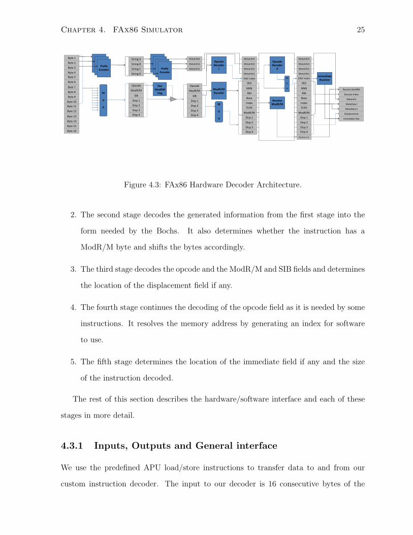
4.3 FAx86 Hardware Decoder Architecture. . . . . . . . . . . . . . . . . . . . 25
5.1 FAx86 and Bochs simulation throughput in MIPS. . . . . . . . . . . . . . 33
5.2 Percentage of Time Spent Decoding Instructions . . . . . . . . . . . . . . 34
5.3 Decoder Hit/Miss Rate . . . . . . . . . . . . . . . . . . . . . . . . . . . . 35
vii
Chapter 1
Introduction
1.1 Motivation
Full-system simulators allow the exploration of different architectural designs, as well as
advanced software development for such architectures. Fast, flexible, and accurate full-
system simulators are necessary for exploring the often vast design spaces and are essential
when simulation is used to aid software development for current or planned designs.
Software simulators are flexible and easy to modify, however, their speed quickly decreases
with the level of detail and accuracy of modeling or when more instrumentation features
are introduced. Software simulation speed also suffers with the number of emulated cores
since a sequential host is simulating parallel processes. This bottleneck in simulation
speed makes it hard for software simulators to scale with the current multi-core system
requirements.
At the other extreme of software-only simulation, are hardware-only simulators which
are implemented in field programmable gate array or FPGA chips. Today, FPGAs are
large and fast enough to provide a way of improving performance and hence capability
over software-only simulators but not without a price. Hardware-only simulators are
less flexible than their counterpart. While the RTL implementation can model timing
1
Chapter 1. Introduction 2
behaviors accurately, modifying the source code for different designs may prove to be
a cumbersome and difficult task. Even after modifying the hardware code, the tedious
process of synthesizing the design is too slow since FPGA CAD tools are still somewhat
primitive. The impact of slow design time, and verification, increases the time-to-market.
As discussed in Chapter 2, hardware-only simulators do not scale well when simulating
large systems and large structures such as multi-megabyte caches since the resources
required to simulate such systems to simulated are often too expensive.
An alternative to hardware-only or software-only simulators is hybrid simulation, in
which only a sufficient portion of the system is emulated in hardware. Hybrid simu-
lators are especially attractive when only a subset of the total system simulation code
contributes to most of the simulation time. Moving those parts to hardware can boost
performance at a low cost while not sacrificing flexibility much. Provided that hardware
simulation acceleration units are of low cost, it also becomes possible to replicate or
multiplex them facilitating many-core system simulation. The complex parts of system
simulation and those that are rarely used can still be emulated in software. Hybrid sim-
ulation is not free of trade-offs. For example, the latency and bandwidth between the
software and the hardware portions of such simulators limits the granularity at which
the two parts can communicate and dictates the performance improvements that may be
possible.
1.2 Objective
We present the progress made in building FAx86, the open-source FPGA-Accelerated
x86 full-system functional simulator. The goal with FAx86 is to port portions of a soft-
ware simulator onto hardware, facilitating faster simulation speed and the simulation of
many-core systems based on the x86 family of processors. The vast majority of today’s
workloads runs on x86 processor-based systems. FAx86 is based on Bochs, a portable
Chapter 1. Introduction 3
open-source IA-32 personal computer simulator written entirely in C++. Bochs simu-
lates modern x86 CPU architectures, runs most operating systems including MS-DOS,
Linux, and Microsoft Windows, and is compatible across various platforms ranging from
a regular desktop machine, to an embedded PowerPC processor.
FAx86’s architecture uses an embedded PowerPC to run the software portion and
implements hardware accelerators, which appear as a soft co-processor. The PowerPC
assigns tasks to the co-processor and communicates with it using a low latency, high
bandwidth interface. The infrastructure allows arbitrary parts of the simulator to be off-
loaded to hardware accelerators. Ultimately, FAx86 aims at accelerating in hardware as
much of the x86 system as possible and necessary. Complicated, rarely used functionality
is to be simulated in software. Common actions that map well on hardware, are to be
simulated in hardware. Given the complexity of the targeted systems, this work presents
the first step in migrating commonly used functions in hardware. In particular, an x86
instruction decoder is presented. Instruction decoding was measured to be the most
time consuming portion of software simulation. In addition, x86 instruction decoding
is complex due to the use of variable length encoding. The presented decoder is of low
cost and high performance. It is pipelined, and can be extended to support decoding for
multicore simulation through time multiplexing. It can also be easily replicated. The
hardware decoder can decode the regular one-byte opcodes, extended opcode groups 1 to
16, SEE types and floating point 16/32 bit x86 instructions. The decoder also supports
2-byte opcodes. Although it is possible to include 3-byte opcodes but we chose to omit
it since the benchmarks do not require such instructions.
1.3 Contributions
The contributions of this work are:
• A Low-cost and modular x86 instruction decoder
Chapter 1. Introduction 4
• An x86 hybrid simulator running on a single FPGA chip
• An Evaluation of FAx86
The current prototype of FAx86 decodes over 90% of x86 instructions and boots Linux
Debian version 2.6. The decoder offers a trade-off between coverage, latency and area.
The performance is evaluated by running several of the SPEC CPU 2006 benchmarks.
FAx86 improves simulation performance over the default Bochs configuration by 5 to
9% depending on the workload. An analysis is given to discuss the reasons behind the
speedup. The simulator will be available online as an open-source code as of Febru-
ary 2011. The website will also provide documentation and guidelines on running the
simulator along with some troubleshooting tips.
1.4 Thesis Structure
The remaining of this thesis proceeds as follows: Chapter 2 overviews the x86 instruction
formats and provides a summary of Bochs simulator. The chapter also includes previous
work in simulation acceleration. Chapter 3 discusses our design and validation method-
ology. Chapter 4 goes over the Fax86’s architecture, the software/hardware interface
and the x86 hardware decoder. In chapter 5 we report the performance of FAx86 and
compare it to other hybrid simulators. Chapter 6 concludes the thesis with a summary
and discusses future work plans.
Chapter 2
Background and Related Work
This chapter serves as the basis needed in order to understand our design choices and
the relevance of our work. FAx86 uses an x86 hardware decoder in conjunction with
a PowerPC. In order to understand why an x86 instruction decoder is non-trivial, we
first introduce the reader to x86 instruction formats and reveal how complex it can be to
decode it as opposed to fixed-length RISC instructions. Then in the following section, we
discuss previous work, in the area of simulation acceleration that influenced our approach.
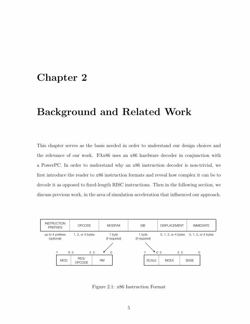
INSTRUCTION
PREFIXESOPCODE MODR/M SIB DISPLACEMENT IMMEDIATE
up to 4 prefixes
(optional)
1, 2, or 3 bytes 1 byte
(if required)
1 byte
(if required)
0, 1, 2, or 4 bytes 0, 1, 2, or 4 bytes
MODREG/
OPCODERM
023567
SCALE INDEX BASE
023567
Figure 2.1: x86 Instruction Format
5
Chapter 2. Background and Related Work 6
2.1 X86 Instruction Format
Mihocka and Shwartsman show that instruction decoding is the most time consuming
part of the Bochs ranging from 20 to 30% of the total eecution time [1]. This is not a
surprise, as x86 is a variable length instruction set that has been evolving over the years.
This section reviews the x86 instruction formats and serves as the basis for describing
the hardware decoder implementation.
Figure 2.1 shows the basic format of x86 instructions. An instruction may use only
some of the fields shown as only the opcode field is mandatory. An instruction may
additionally include several instruction prefixes, an addressing form specifier consisting
of a ModR/M byte and optionally of a SIB (Scale-Index-Base) byte, a displacement, and
an immediate field [2].
2.1.1 Instruction Prefixes
There are four different groups of instruction prefixes. For each instruction, only up to
one prefix code from each of the groups is useful. Prefixes can be placed in any order. The
first group consists of the lock and repeat prefixes. A lock prefix ensures atomic access
to shared memory whereas the repeat prefixes cause the instruction to be repeated for a
number of times as specified by a register value. Group two consists of segment override
prefixes, which change the memory segment accessed by the instruction. Group three is
the operand size override prefix, which allows switching between 16-bit and 32-bit operand
sizes. Group four is the address size override prefix, and allows switching between 16-bit
and 32-bit addressing modes. Although it is possible to have more than a single prefix
byte belonging to the same group, or more than 4 prefix bytes, the outcome of such an
instruction causes an unpredictable behavior.
Chapter 2. Background and Related Work 7
2.1.2 Opcodes
The opcode can be one through three bytes in length. An additional 3-bit opcode field
appears in the ModR/M byte that may follow the opcode. For some opcodes, smaller
fields can be defined within the primary opcode itself. These fields can define, displace-
ment sizes, condition codes, sign extension modes. It can also specify a direction for
the operation by specifying which of the operands is source and which is a destination.
The encoding fields used by an opcode vary depending on the operation class. Two-byte
opcodes start with the escape byte 0x0F as their first byte followed by an opcode byte.
Three-byte opcode also start with 0x0F as their first byte, followed by 0x38 or 0x3A,
then an opcode byte.
2.1.3 ModR/M and SIB Bytes
Unlike a load/store architecture like SPARC or MIPS, X86 allows memory locations to
be used directly as operands. The optional ModR/M byte follows the opcode byte(s)
as an addressing form specifier. As Figure 2.1 shows, the ModR/M byte consists of
three inter-dependent fields: (1) The Mod field which combined with the R/M field
allows for 32 different addressing forms. These forms are used for direct access to the
eight registers (when Mod is 0b11) and for specifying the 24 memory addressing modes.
(2) The Reg/Opcode field either specifies a register number or three bits of opcode
information. The primary opcode determines the purpose of the Reg/Opcode field in
this case. (3) Finally, the R/M field either specifies a register as an operand, or it is
combined with the Mod field to encode an addressing mode.
Some encodings of the ModR/M byte require a second addressing byte, the Scale-
Index-Base or simply the SIB byte. This byte includes three fields. The Scale field
specifies a scale factor. The Index field identifies the register number for the index
register. The Base field identifies the register number of the base register. In order to
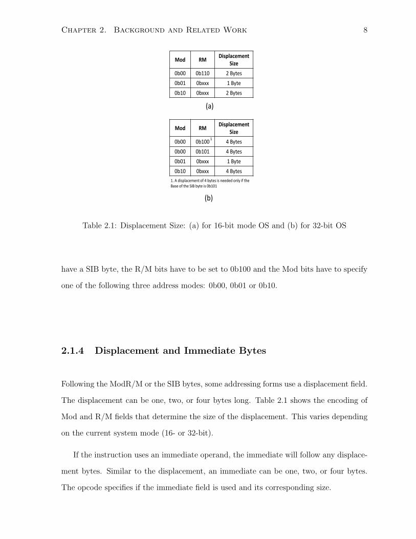
Chapter 2. Background and Related Work 8
Mod RMDisplacement
Size
0b00 0b100 4 Bytes
0b00 0b101 4 Bytes
0b01 0bxxx 1 Byte
0b10 0bxxx 4 Bytes
1
1. A displacement of 4 bytes is needed only if the Base of the SIB byte is 0b101
Mod RMDisplacement
Size
0b00 0b110 2 Bytes
0b01 0bxxx 1 Byte
0b10 0bxxx 2 Bytes
(a)
(b)
Table 2.1: Displacement Size: (a) for 16-bit mode OS and (b) for 32-bit OS
have a SIB byte, the R/M bits have to be set to 0b100 and the Mod bits have to specify
one of the following three address modes: 0b00, 0b01 or 0b10.
2.1.4 Displacement and Immediate Bytes
Following the ModR/M or the SIB bytes, some addressing forms use a displacement field.
The displacement can be one, two, or four bytes long. Table 2.1 shows the encoding of
Mod and R/M fields that determine the size of the displacement. This varies depending
on the current system mode (16- or 32-bit).
If the instruction uses an immediate operand, the immediate will follow any displace-
ment bytes. Similar to the displacement, an immediate can be one, two, or four bytes.
The opcode specifies if the immediate field is used and its corresponding size.
Chapter 2. Background and Related Work 9
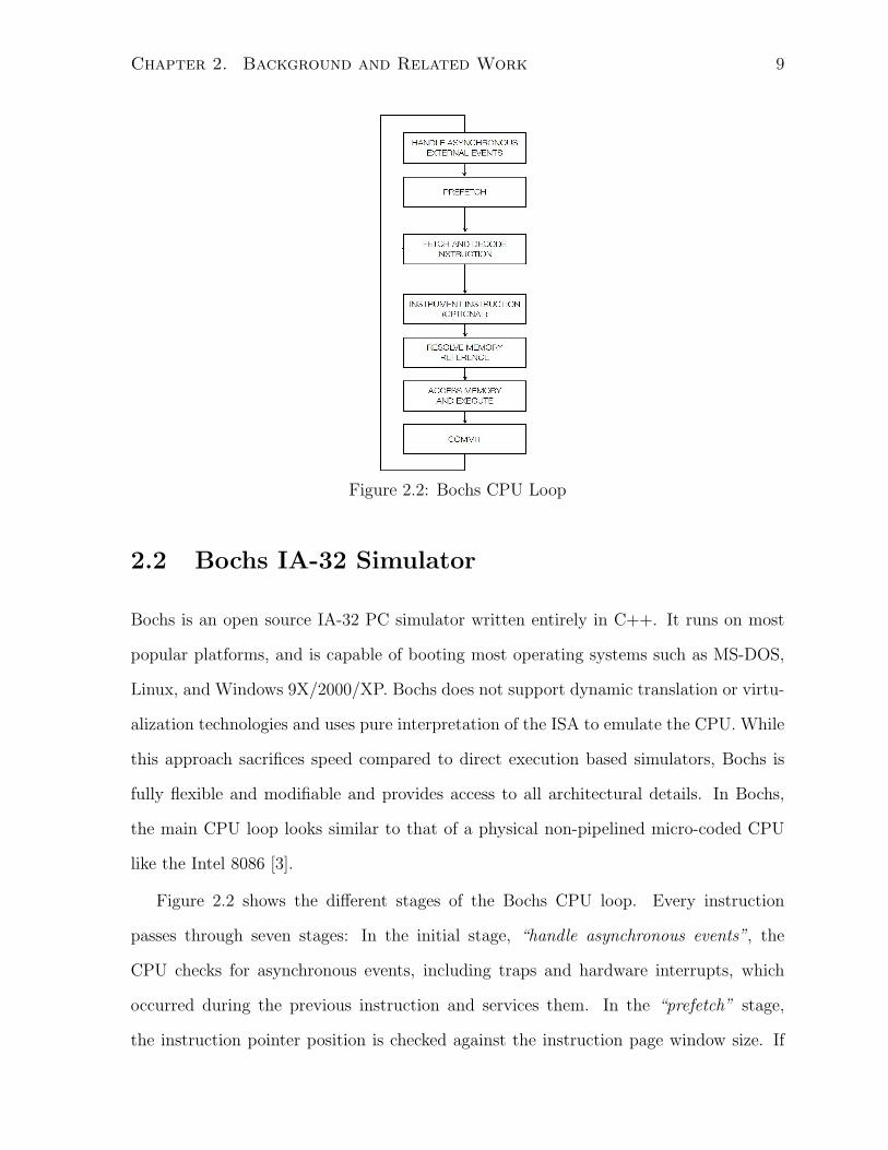
Figure 2.2: Bochs CPU Loop
2.2 Bochs IA-32 Simulator
Bochs is an open source IA-32 PC simulator written entirely in C++. It runs on most
popular platforms, and is capable of booting most operating systems such as MS-DOS,
Linux, and Windows 9X/2000/XP. Bochs does not support dynamic translation or virtu-
alization technologies and uses pure interpretation of the ISA to emulate the CPU. While
this approach sacrifices speed compared to direct execution based simulators, Bochs is
fully flexible and modifiable and provides access to all architectural details. In Bochs,
the main CPU loop looks similar to that of a physical non-pipelined micro-coded CPU
like the Intel 8086 [3].
Figure 2.2 shows the different stages of the Bochs CPU loop. Every instruction
passes through seven stages: In the initial stage, “handle asynchronous events”, the
CPU checks for asynchronous events, including traps and hardware interrupts, which
occurred during the previous instruction and services them. In the “prefetch” stage,
the instruction pointer position is checked against the instruction page window size. If
Chapter 2. Background and Related Work 10
0
10
20
30
40
50
60
70
Astar Boot GCC h264 lbm omnetpp soplex libquantum
Pe
rce
nta
ge o
f ti
me
Benchmark
ReadHandler
ReadPhysicalPage
CPULoop
TranslateLinear
WritePhysicalPage
FetchDecode32
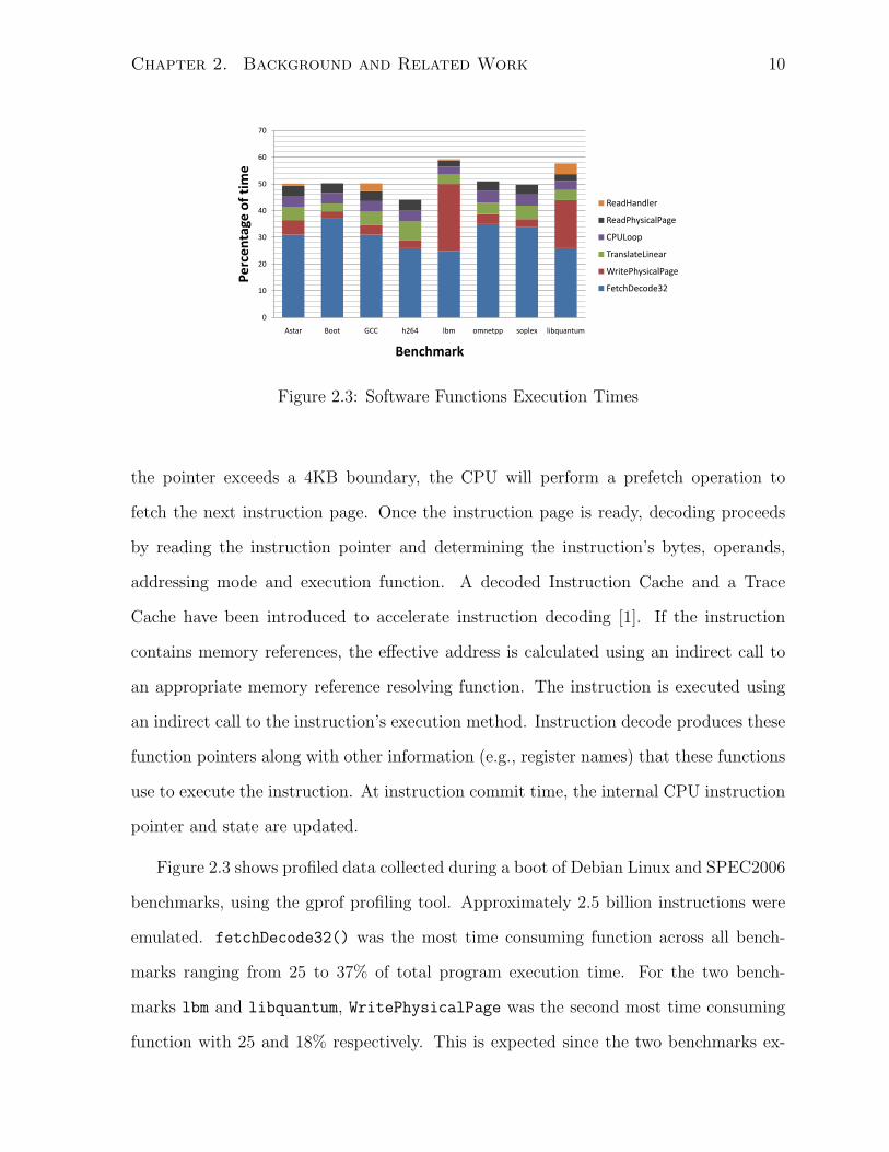
Figure 2.3: Software Functions Execution Times
the pointer exceeds a 4KB boundary, the CPU will perform a prefetch operation to
fetch the next instruction page. Once the instruction page is ready, decoding proceeds
by reading the instruction pointer and determining the instruction’s bytes, operands,
addressing mode and execution function. A decoded Instruction Cache and a Trace
Cache have been introduced to accelerate instruction decoding [1]. If the instruction
contains memory references, the effective address is calculated using an indirect call to
an appropriate memory reference resolving function. The instruction is executed using
an indirect call to the instruction’s execution method. Instruction decode produces these
function pointers along with other information (e.g., register names) that these functions
use to execute the instruction. At instruction commit time, the internal CPU instruction
pointer and state are updated.
Figure 2.3 shows profiled data collected during a boot of Debian Linux and SPEC2006
benchmarks, using the gprof profiling tool. Approximately 2.5 billion instructions were
emulated. fetchDecode32() was the most time consuming function across all bench-
marks ranging from 25 to 37% of total program execution time. For the two bench-
marks lbm and libquantum, WritePhysicalPage was the second most time consuming
function with 25 and 18% respectively. This is expected since the two benchmarks ex-
Chapter 2. Background and Related Work 11
Execute Pointer
Resolve ModRM
MetfInfo4 MetfInfo3 MetfInfo2 MetfInfo1
SEG DEST NNN RM
Base Index Scale ModRM
Displacement
Immediate
0
4
8
12
16
20
24
28
Byte 3 Byte 2 Byte 1 Byte 0
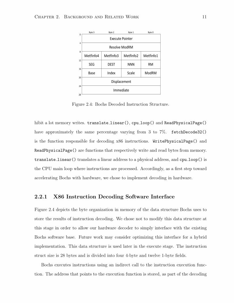
Figure 2.4: Bochs Decoded Instruction Structure.
hibit a lot memory writes. translate linear(), cpu loop() and ReadPhysicalPage()
have approximately the same percentage varying from 3 to 7%. fetchDecode32()
is the function responsible for decoding x86 instructions. WritePhysicalPage() and
ReadPhysicalPage() are functions that respectively write and read bytes from memory.
translate linear() translates a linear address to a physical address, and cpu loop() is
the CPU main loop where instructions are processed. Accordingly, as a first step toward
accelerating Bochs with hardware, we chose to implement decoding in hardware.
2.2.1 X86 Instruction Decoding Software Interface
Figure 2.4 depicts the byte organization in memory of the data structure Bochs uses to
store the results of instruction decoding. We chose not to modify this data structure at
this stage in order to allow our hardware decoder to simply interface with the existing
Bochs software base. Future work may consider optimizing this interface for a hybrid
implementation. This data structure is used later in the execute stage. The instruction
struct size is 28 bytes and is divided into four 4-byte and twelve 1-byte fields.
Bochs executes instructions using an indirect call to the instruction execution func-
tion. The address that points to the execution function is stored, as part of the decoding
Chapter 2. Background and Related Work 12
process, in the Execute Pointer field. The Resolve Mod/Rm field contains the address
that points to the function that calculates the corresponding memory address. MetaInfo4
holds a flag bit that is set when a 2-byte opcode exists. MetaInfo3 stores the actual op-
code byte. MetaInfo2 contains the length of the instruction. The length of the instruction
is useful for a number of tasks including that of moving the fetch instruction pointer.
MetaInfo1 is used to set the flags for the operating system and the addressing modes (16
or 32-bit modes). The Mod/Rm and SIB ’s subfields depicted in Figure 2.1 are stored
each in its corresponding field in the instruction structure. Finally, the last eight bytes
are reserved for the displacement and Immediate. The displacement field is used for
resolving memory references while the immediate field is used in regular data processing
operations.
Bochs follows a simple sequential algorithm to decode x86 instructions. The algorithm
processes one byte at a time, updating each field affected by the decoded byte. There
are four main stages in the algorithm: 1) Prefix Decode, 2) ModRM/SIB/Displacement
Decode, 3) Opcode Decode, and 4) Immediate Decode.
Prefix Decode
Prefix Decode is implemented as a single switch statement over the byte in question.
There are 12 byte values that correspond to the four groups of prefixes. When the
byte matches a prefix value, the corresponding fields in the instruction struct will be
updated. The fetch instruction pointer is then incremented to decode the second byte.
The algorithm will keep on looping until it decodes all of the prefixes. The software does
not keep track of the number of prefixes from each group or the number of prefixes in
total. For instance, in the case where more than one prefix of a single group occurs, the
second byte will overwrite the first due to the sequential behavior of the program. This
is allowed to occur in real instruction but since the behavior is unpredictable, software
can detect an error in the instruction when decoding an opcode. Bochs will then exit
Chapter 2. Background and Related Work 13
with a Panic message.
ModRm/SIB/Displacement Decode
As discussed in Section 2.1.2 the opcode determines if a Mod/RM byte is needed. Simi-
larly, the Mod and RM subfields determine if a SIB byte is needed. In turn, the Mod/RM
(and SIB) byte(s) determine the displacement’s size (0, 8, 16, or 32 bits). In the order
mentioned previously, the algorithm checks the bits for any particular match and sets
the corresponding fields in the instruction structure.
Opcode Decode
The goal of opcode decode is, among other things, to decide which execute function needs
to be invoked to execute the instruction. The basic idea is to use the opcode as an index
to a flat array (or map) which returns the address of the execute function. Unfortunately,
the opcode alone is not sufficient to determine the right function index. Several other
pieces of the instruction’s format need to be considered. Accordingly, the size of a flat
map table would be in the order of several gigabytes. Instead, Bochs uses a set of decoding
arrays organized hierarchically. The first level divides opcodes into two different sets. In
the first set are the opcodes that do not use any extensions. The second set holds the
opcodes that use the ModR/M or SSE prefix field bits as opcode extensions. The second
set is divided into five opcode subgroups: Group N, Group RM, Group 3-byte, Group
SSE, and Group FP Escape. Each group uses several more bits from Mod/RM or SSE
prefix fields as index to access smaller arrays. The algorithm checks the opcode against
the first set. If there is a hit, the function index is then retrieved. If not, then the table
returns an address to the second set of arrays. The second set has about 350 arrays
shared by all the opcodes. These arrays will either generate a pointer to another one of
the 350 arrays, or the proper function index. Once the function index is determined, the
function address is looked up and stored in the Execution Pointer field.
Chapter 2. Background and Related Work 14
Immediate Decode
After the Opcode decode, an attribute is retrieved from the arrays. This attribute con-
tains a 4-bit immediate mode specifier. A switch statement, based on the immediate
specifier, takes care of fetching immediate bytes and storing them in the instruction
structure.
2.3 Related Work
Several software-based x86 simulators exist. The popular ones include Virtutech Simics,
a full-system software simulator[4]. Simics supports a range of architectures including
UltraSPARC, Alpha and x86. The simulator only models functional behavior. Users have
to develop their own timing models. Support for incorporating timing models into Simics
may not exist in future versions. Another academically popular simulator is PTLsim.
PTLsim models a modern superscalar out-of-order x86-64 processor core [5]. PTLsim
translates x86 instructions into micro-ops. PTLsim uses inline x86 assembly language,
for simulation acceleration. QEMU is an x86 emulator that also relies on direct execution
for improving speed [6]. Bochs is an open-source full-system x86 simulator where each
instruction is emulated completely in software. We chose Bochs as the basis for FAx86
since it is open-source and does not use direct execution making it portable to embedded
processors.
Several hybrid simulators exist. ProtoFlex is based on SimFlex [7] and models the
UltraSPARC architecture [8]. ProtoFlex runs most common SPARC instructions in their
entirety using a BlueSPARC core. BlueSPARC only captures the functional behavior of
the most common and simple instructions of the UltraSPARC III. Complex instructions
and devices that are too difficult to model in hardware are handled by Simics software
running on a regular desktop machine. FAx86 follows ProtoFlex’s approach to model an
x86 system where the most common operations are mapped onto hardware. FAST is a
Chapter 2. Background and Related Work 15
hybrid x86 simulator [9]. It uses QEMU for emulating x86 instructions and off-loads the
timing model onto hardware. HASIM off-loads functional and timing to hardware [10].
A number of RAMP projects have also emerged notably RAMP blue, RAMP red and
most recently RAMP GOLD [11] [12] [13]. RAMP Gold is an FPGA-based architecture
simulator that simulates a 64-core shared-memory target machine. RAMP Gold’s policy
is to separate between the functional model and the timing model similarly to FAST.
However, both models are implemented in a single FPGA. The functional model is a
64-thread feed-through pipeline with each thread simulating an independent target core.
The functional model implements the full SPARC V8 ISA in hardware, including complex
functional units such as floating point, precise exceptions, MMUs, timers and interrupt
controllers. The simulator is able to run an operating system, booting for example Linux
2.6.21 kernel. The timing model is implemented on the same FPGA chip with private
L1 instruction and data caches for each simulated core. All the cores share one L2 cache.
On the Virtex-5 LX110T FPGA, RAMP GOLD can support up to 12MB of total target
cache. RAMP Gold achieves speedup of two orders of magnitude when compared with
common software-based architecture simulators.
Where most of the previous work being done aims at modeling simpler architectures
such as SPARC, FAx86 is an attempt at modeling one of the most popular and complex
architecture available nowadays. x86 architecture is widely used. Realistic workloads and
applications are accessible and can be of great help in improving architecture exploration.
FAx86’s approach differs from ProtoFlex and FAST in the sense that the full system
is modeled in the FPGA and no communication is needed with an external Desktop
machine. RAMP Gold implements a SPARC V8 soft core for the simulation purposes.
FAx86 uses a PowerPC to model the complex implementations of an x86 architecture and
has hardware to support time-consuming sections of the software. While FAx86 is still
not mature enough for a fair performance comparison with pervious works, we present
evidence of its potentials.
Chapter 3
Methodology
3.1 Design Environment
We used the Bochs 2.3.7 release source tree obtained from the Bochs website to develop
our hybrid system. We cross-compiled Bochs for the PowerPC using the gcc/g++ com-
pilers contained in the Embedded Linux Development Kit (ELDK) version 4.2 tool-chain.
Bochs requires a disk image for booting an operating system. We created a Debian Linux
image using kernel packages that support our FPGA board. The FPGA board is a Xilinx
ML-507 board. Its features include a Virtex-5 FPGA chip, common peripherals such as
PCIe, Ethernet, USB and RS-232. The FPGA chip also contains an embedded hard
PowerPC processor.
We used the Xilinx Integrated Synthesis Environment (ISE) design suite version 10.1
for HDL development, synthesis, place-and-route, and the ISE simulator for design sim-
ulation purposes. We used the Xilinx Platform Studio (XPS) version 10.1 to generate
a system-on-chip, including a PowerPC and peripheral interfaces such as the Auxiliary
Processor Unit bus controller. The Virtex-5 bitstream is compiled by Xilinx ISE and
downloaded via JTAG. The JTAG interface also allows PowerPC debugging by read-
ing/writing to arbitrary memory, changing status registers, and halting the processor.
16
Chapter 3. Methodology 17
The Xilinx Embedded Development Kit (EDK), based on the GNU tool-chain, includes
a C compiler for the PowerPC 440 that provides wrappers for custom PowerPC instruc-
tions, including the APU load/store instructions that we used in our design.
3.2 Design, Simulation and Verification
In the initial development phase we developed the software interface for the hardware
decoder. The second phase of the project involved building the x86 decoder on the FPGA.
In this stage, we proceeded to incrementally move parts of the software decoding onto
hardware. We used Bochs to study application behavior and thus to justify various design
choices. Bochs also served as our functional specification for modeling x86 behavior. Our
hardware decoder attempts to follow the Bochs design as closely as possible. The hybrid
nature of our system and its reliance on the software simulator to handle the remaining
portions of the CPU behavior, constrains our design to use a specific set of inputs and
outputs but does not affect the internal functional components.
For each decoder module, we went through a multi-step process of simulation and
verification. In the first step, we isolate the chunk of software that is going to be im-
plemented in hardware. For example, we isolated prefix decoding by defining the set of
input/outputs required and the instruction struct fields that are affected by the prefix
decode stage. Then we implemented the prefix decoder and validated it by comparing its
output with its software counterpart. We incrementally modified the design to increase
parallelism where possible. Any modification to the decoder design was first implemented
in software (as part of the Bochs decoding algorithm) and tested to ensure its integrity.
After writing the HDL code for the unit in question, we verified its functionality with
a couple of test cases (simple x86 instructions) using the ISEsim simulator. Before in-
corporating the hardware unit into our hybrid system, we performed hardware/software
co-simulation, checking that the intermediate results, as well as the final output, matched
Chapter 3. Methodology 18
for each decoded instruction. The load/store interface of the APU proved helpful in our
debugging efforts, allowing us to easily pass information between software and hardware,
serving as a clean boundary between the two. In the last step, we removed the software
portion of the code and replaced it entirely with our hardware block, examining the
Bochs output and log files to verify the correct behavior of the decoder. We performed
all of the above steps for developing each individual unit, and incrementally added it to
our system. Validation was performed by booting the Linux kernel and running several
SPEC CPU 2006 benchmarks. It is possible that errors may have gone undetected, how-
ever, given that the system correctly boots Linux and runs several SPEC benchmarks we
believe that they are unlikely.
Chapter 4
FAx86 Simulator
This section describes the architectural design of FAx86. The first subsection describes
the system infrastructure, and how the software simulator and the hardware blocks in-
terface. The next subsection describes the x86 Instruction Decode Unit.
4.1 System Overview
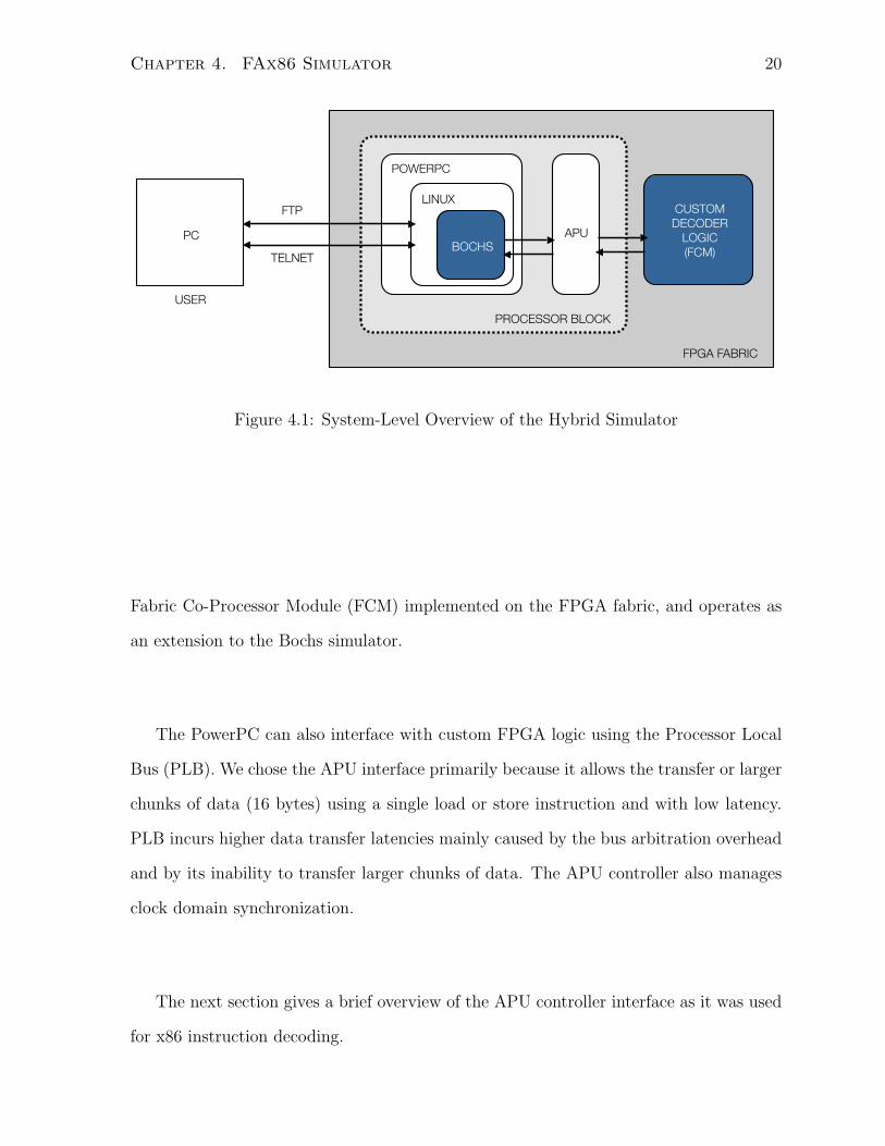
Figure 4.1 shows the setup of our hybrid system. FAx86 was implemented on the Xilinx
ML507 development board with a 400MHz embedded PowerPC processor. Bochs is run
on a PowerPC-based Debian Linux distribution, and emulates an IA-32 PC running
Debian Linux version 2.6. Telnet and FTP servers running on the non-emulated OS
allow us to interact with Bochs and copy files to and from the system on board. A 4GB
compact flash disk was used to store Bochs’ executable along with the library files needed
to run the simulator. The same flash disk was used to store the simulated OS disk image.
A serial port was used for kernel debugging.
The instruction decoder interfaces with the PowerPC through the Auxiliary Process-
ing Unit (APU) interface [14],[15]. The APU enables flexible, low-latency, and high-
bandwidth data transfers between the processor and custom logic, as the PowerPC pro-
cessor is tightly coupled with the APU controller. Our instruction decoder is built as a
19
Chapter 4. FAx86 Simulator 20
POWERPC
PC
USER
FPGA FABRIC
PROCESSOR BLOCK
APU
CUSTOM
DECODER
LOGIC
(FCM)
LINUX
BOCHS
FTP
TELNET
Figure 4.1: System-Level Overview of the Hybrid Simulator
Fabric Co-Processor Module (FCM) implemented on the FPGA fabric, and operates as
an extension to the Bochs simulator.
The PowerPC can also interface with custom FPGA logic using the Processor Local
Bus (PLB). We chose the APU interface primarily because it allows the transfer or larger
chunks of data (16 bytes) using a single load or store instruction and with low latency.
PLB incurs higher data transfer latencies mainly caused by the bus arbitration overhead
and by its inability to transfer larger chunks of data. The APU controller also manages
clock domain synchronization.
The next section gives a brief overview of the APU controller interface as it was used
for x86 instruction decoding.
Chapter 4. FAx86 Simulator 21
DECODE STAGE
EXECUTE STAGE
WRITEBACK
STAGE
DECODE
Resynchro
niz
ation Inte
rface
FCM
CUSTOM BLOCK
POWERPC APU CONTROLLER FCM
LOAD/WB
STAGE
LOAD DATA
RESULT
FETCH STAGE
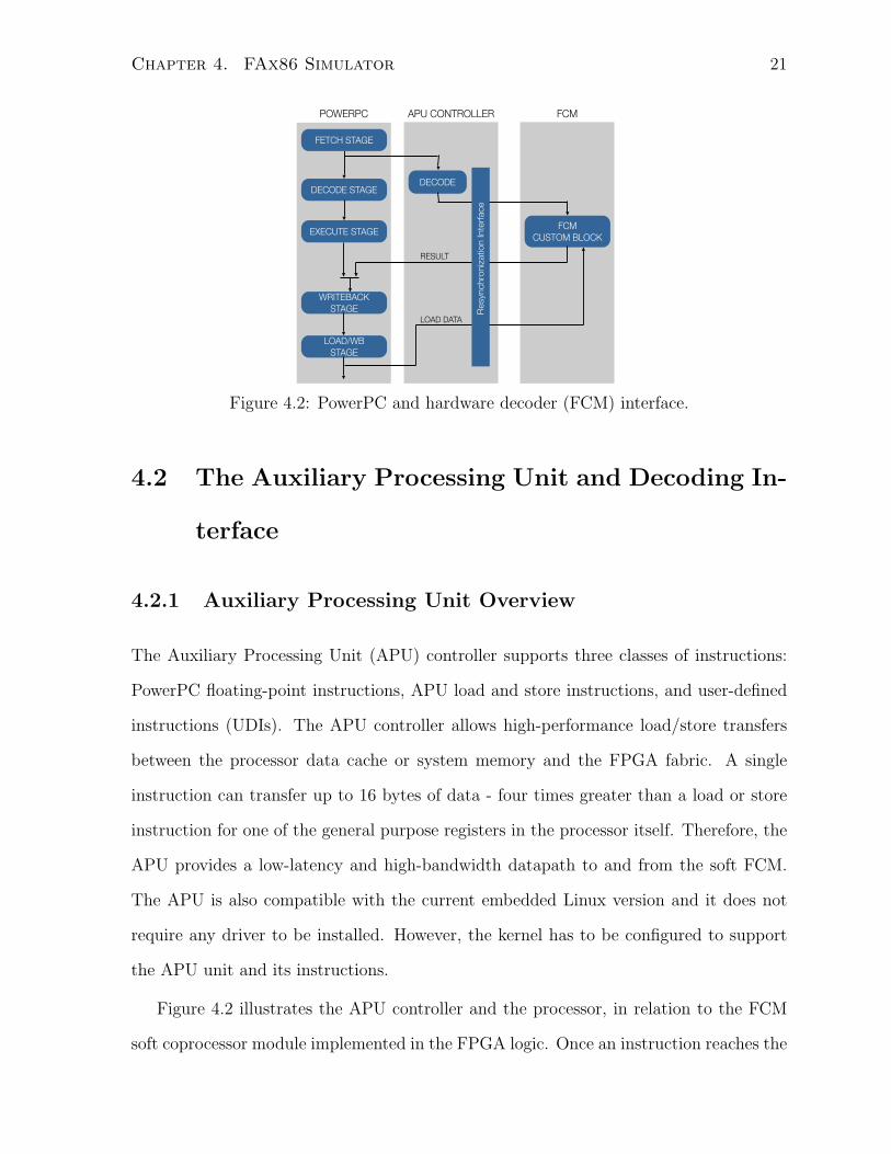
Figure 4.2: PowerPC and hardware decoder (FCM) interface.
4.2 The Auxiliary Processing Unit and Decoding In-
terface
4.2.1 Auxiliary Processing Unit Overview
The Auxiliary Processing Unit (APU) controller supports three classes of instructions:
PowerPC floating-point instructions, APU load and store instructions, and user-defined
instructions (UDIs). The APU controller allows high-performance load/store transfers
between the processor data cache or system memory and the FPGA fabric. A single
instruction can transfer up to 16 bytes of data - four times greater than a load or store
instruction for one of the general purpose registers in the processor itself. Therefore, the
APU provides a low-latency and high-bandwidth datapath to and from the soft FCM.
The APU is also compatible with the current embedded Linux version and it does not
require any driver to be installed. However, the kernel has to be configured to support
the APU unit and its instructions.
Figure 4.2 illustrates the APU controller and the processor, in relation to the FCM
soft coprocessor module implemented in the FPGA logic. Once an instruction reaches the
Chapter 4. FAx86 Simulator 22
decode stage, it is simultaneously decoded by both the CPU and APU decoder blocks. If
the instruction is intended for the FCM block, the CPU looks for a response from the APU
controller. The APU then fetches the necessary operands from the processor memory and
passes it to the FCM for processing. Depending on the type of instruction (autonomous
vs non-autonomous), the CPU will either wait, or continues with the program execution.
Because the PowerPC processor and the FCM reside in two separate clock domains,
synchronization modules of the APU controller manage the clock frequency difference.
This allows the FCM to operate at a slower frequency than the processor. In this case, the
APU controller receives the resultant data from the coprocessor and at the proper execu-
tion time sends the data back to the processor. The frequency of the APU cannot be ar-
bitrarily different than that of the processor. In order to achieve synchronization between
the two domains, the APU requires the FCM clock frequency be Processorfrequency/N
where N is an integer between 1 and 16. In this prototype of FAx86, the clock frequency
ratio is 1:2 since the PowerPC runs at 400MHz and the FCM at 200MHz.
Software programs access the FCM from within assembler or C code. Assembler
mnemonics are available for user-defined instructions and the pre-defined load/store in-
structions, enabling programmers to invoke hardware functions inside the regular pro-
gram flow.
4.2.2 APU Instructions Overview
The APU instructions can be autonomous or non-autonomous. Non-autonomous in-
structions require data to be returned to the processor, therefore incurring stalls in the
pipeline. Autonomous instructions on the other hand, are fire-and-forget type of instruc-
tions. In our design, the load/store instructions are non-autonomous, which means that
the CPU pipeline stalls while the FCM is operating on an instruction. This allows us to
implement synchronization semantics to pace the software execution with the hardware
FCM latency. Load/store instructions can use data types whose length varies between
Chapter 4. FAx86 Simulator 23
1 byte and 16 bytes. Since the largest x86 instruction is 15 bytes, 16-byte Load/Store
instructions were used to send instruction bytes for decoding with the APU. APU loads
and stores have to be aligned in memory and this represents a challenge when the set
of instruction bytes to be decoded does not start at a 16-byte boundary. Our hardware
decoder uses a buffer to avoid splitting misaligned loads into two loads as explained in
the next section.
The PowerPC needs to determine when an instruction is available to store and if this
instruction is valid. Load/Store instructions are not suitable for monitoring the decoder
as there are intrinsic performance overheads with processing memory operations. We
opted to allow software to poll the hardware decoder via user-defined instructions (UDI).
A UDI can read/write from/to the decoder’s status register, therefore granting software
total control over the hardware without the overheads of load/store processing. In order
to avoid any illegal instructions, both the kernel and the bitstream need to be configured
to support UDIs.
4.2.3 FCM Decoding Interface
Referring back to figure: 4.2, the APU and the FCM abide by a communication pro-
tocol that governs data transfer between the two domains. Therefore, software functions
from the APU side communicate with a finite state machine from the hardware side. Al-
gorithm 1 illustrates the software algorithm that communicates with the hardware finite
state machine. The decoder simply decodes a stream of bytes without any regards to
whether a branch instruction is executed, therefore, software has to check for branch exe-
cutions before fetching instructions for the decoder. The next step involves reading from
the status register to determine whether the decoded instruction is valid to be stored.
The status register is explained, in more details, in the next section. The hardware finite
state machine is responsible of activating and resetting the decoder and acknowledging
software commands, as well as loading/storing instructions.
Chapter 4. FAx86 Simulator 24
Algorithm 1 Software Interface Algorithm
if Branch is detected then
Perform LOAD
end if
READ STATUS REGISTER
if STATUS IS VALID then
STORE INSTRUCTION
else if STATUS IS GARBAGE then
goto: LOAD
else if STATUS IS PREFIX/OPCODE ERROR then
goto: SOFTWARE DECODE
end if
DECODE REMAINING BYTES
4.3 FAx86 Hardware Decoder Architecture
In this section, we present a decoder design that is able to decode most x86 instruction
formats in hardware. Figure 4.3 shows a high-level overview of the decoder. The decoder
is pipelined. It is relatively straightforward to remove pipeline stages and thus reduce
the amount of decoding that happens in hardware. While we have implemented a full-
blown decoder in hardware, the design we present does not include those stages that
we found were used sparingly. Removing those stages reduced pipeline depth, increased
the operating frequency and led to higher overall performance. Since we are bounded
by the software interface, we attempted to closely follow Bochs’ decoding scheme, while
exploiting as much parallelism as possible with the available hardware.
Decoding proceeds over five pipeline stages:
1. The first stage reads the first three bytes, generates encoded information about
them and shifts the input bytes accordingly for the next stage to use.
Chapter 4. FAx86 Simulator 25
Byte 1
Byte 2
Byte 3
Byte 4
Byte 5
Byte 6
Byte 7
Byte 8
Byte 9
Byte 10
Byte 11
Byte 12
Byte 13
Byte 14
Byte 15
Byte 16
PrefixEncoder
M
U
X
String A
String B
String C
String D
Opcode
ModR/M
SIB
Disp 1
Disp 2
Disp 3
Disp 4
PrefixEncoder
Has ModRM
Flag
MetaInfo4
MetaInfo2
MetaInfo1
Opcode
ModR/M
SIB
Disp 1
Disp 2
Disp 3
Disp 4
OpcodeDecoder
I
ModR/MDecoder
M
U
X
MetaInfo4
MetaInfo3
MetaInfo2
MetaInfo1
EXEC Index
SEG
NNN
RM
Base
Index
Scale
ModR/M
Disp 1
Disp 2
Disp 3
Disp 4
MetaInfo4
MetaInfo3
MetaInfo2
MetaInfo1
OpcodeDecoder
II
M
U
X
EXEC Index
ResolveModR/M
SEG
NNN
RM
Base
Index
Scale
ModR/M
Disp 1
Disp 2
Disp 3
Disp 4
Resolve Ind.
ImmediateResolver
Resolve ModRM
Execute Index
MetaInfo
MetaData I
MetaData II
Displacement
Immediate Size
Figure 4.3: FAx86 Hardware Decoder Architecture.
2. The second stage decodes the generated information from the first stage into the
form needed by the Bochs. It also determines whether the instruction has a
ModR/M byte and shifts the bytes accordingly.
3. The third stage decodes the opcode and the ModR/M and SIB fields and determines
the location of the displacement field if any.
4. The fourth stage continues the decoding of the opcode field as it is needed by some
instructions. It resolves the memory address by generating an index for software
to use.
5. The fifth stage determines the location of the immediate field if any and the size
of the instruction decoded.
The rest of this section describes the hardware/software interface and each of these
stages in more detail.
4.3.1 Inputs, Outputs and General interface
We use the predefined APU load/store instructions to transfer data to and from our
custom instruction decoder. The input to our decoder is 16 consecutive bytes of the
Chapter 4. FAx86 Simulator 26
instruction stream. The maximum length of an x86 instruction is 15 bytes with three
to five bytes being most common in practice. A naive implementation will use a load
instruction to load 16 bytes anew starting from the current instruction pointer before
invoking the decoder. Two load operations would be needed if the starting address is not
aligned. In order to reduce the number of loads necessary and thus improve performance,
a better decoder design would try to decode as many instructions as possible each time
a 16-byte chunk is loaded. Our hardware decoder uses an input shift register and logic
to achieve this. The operation of this shift register is described in later section in more
detail.
The output of the fetchDecode() function is a data structure called bxInstruction c
with a layout matching the output of our decoder, as shown in Figure 2.4. The data lay-
out in hardware matches the data structure’s layout, which allows the output of the
decoder to be copied directly to the Bochs instruction structure. This is to minimize
swizzling of the data structure in software after copying.
The decoder does not generate the full instruction structure. It returns the 16 bytes
which cover the Metainfo, Metadata and displacement fields. The immediate field is
decoded in hardware but the immediate bytes are never returned to software. The rea-
son behind it is that the extraction of the immediate bytes from the byte-stream adds
hardware complexity to the design which will then lead to a decrease in the maximum
operated clock frequency, and an increase in the number of pipeline stages. We found
it to be better to report to software where to get the immediate from memory. The
hardware decoder sends three concatenated indexes back to software. Those indexes are
retrieved using the fast user defined instructions. The first index is a pointer to where the
immediate bytes are. The second index determines the address of the address calculation
function, and the last index is used to retrieve the address of the execution function.
Since loading and storing introduces latency, we try to keep memory accesses as low
as possible. In order to know when to load bytes into the hardware decoder and when
Chapter 4. FAx86 Simulator 27
to read a decoded instruction, the software needs to probe the hardware for any change
in its state. We chose the simplicity of a status register. The status register reports
the current state of the hardware decoder and can be read directly by software using
a UDI. There are five possible states available: Idle, Garbage, Prefix Error, Opcode
Error, and Ready. The Garbage state occurs when the decoder does not have enough
bytes left to decode an instruction and hence its current output is meaningless. The
decoder design shown decodes up to three prefixes as we found that four prefixes occur
rarely. In the rare case of a fourth prefix, the hardware will transition into the prefix
error state which will then trigger the software decode function. Similarly, the opcode
error state is set when an instruction opcode is not supported. Software will then take
over decoding the unsupported opcode. The ready state informs software of an available
decoded instruction.
4.3.2 Input Shift Register
To reduce the number of loads that is needed to ensure correct instruction decoding
the hardware decoder uses the input shift register (ISR). The ISR is loaded with 16
bytes. As long as the next instruction to be decoded falls within these 16 bytes no
additional loads are needed. Once the current instruction is decoded, ISR ejects the
decoded bytes so that decoding can proceed with the next instruction. The input shift
register improves decoding performance as typically a single load results in four or more
decoded instructions. If all of the bytes in the register have been decoded or not enough
bytes are left to decode an instruction, the control unit sets the Garbage flag in the status
register to indicate for software that the following decoded instruction is incomplete.
4.3.3 Prefix Encoding and Decoding Stages
As mentioned in Section 2.1.1, an instruction can have up to four different prefix bytes,
each belonging to a distinct prefix group. However, we found out that rarely an instruc-
Chapter 4. FAx86 Simulator 28
tion contains four prefixes and hence chose to present the design that can decode up to
three prefixes. The prefix encoder examines the first three bytes of the instruction stream
in parallel, comparing each byte to the predefined prefix byte encodings and the two-byte
opcode escape byte value. The prefix encoder generates four encoded bit strings: Each
bit string contains a 3-bit header. The first, second and third bits correspond respectively
to the first, second and third bytes in the instruction stream. If a bit is set, then its cor-
responding byte is a prefix. Each of the encoded bit strings contains relevant information
that can be extracted from the three decoded prefixes simultaneously. The header is also
used as a select signal for a multiplexer that filters the original instruction stream and
extracts the opcode along with the next six additional bytes.
4.3.4 Opcode, ModR/M, SIB, Displacement Decoding Stage
Due to the variable-length instruction format, determining the location of the various
fields within an instruction is implemented as a serial operation in Bochs. The location
of each field depends on the meaning of the fields that come before it. In contrast, our
decoder exploits parallelism. For instance, we do not care about any dependence between
the opcode and the ModRM/SIB and therefore we simply decode them simultaneously.
The opcode decoder determines whether a ModR/M byte follows the opcode. This
information is looked up in a table indexed by the opcode. The output of the opcode
decoder is three bit vectors to be used by the second opcode decoder. The first vector is
an index to the second opcode decoder and a flag that determines if the second decoder
has to be used. The second vector is an index to the corresponding function in software.
The third vector determines if the opcode has an Immediate field. The ModR/M decoder
acts as both ModR/M and SIB decoder simultaneously. The ModR/M decoder extracts
the fields in the ModR/M and SIB bytes. The ModR/M decoder also determines whether
a SIB byte follows, based on the R/M field of the ModR/M byte. The extracted fields
are: Scale, Index, Base for the SIB byte and MODRM, RM, NNN for the ModR/M
Chapter 4. FAx86 Simulator 29
byte. The ModR/M decoder also generates control signals to multiplex the displacement
bytes. Based on the Mod and R/M fields of the ModR/M byte, and the Base field of
the SIB byte, the number of bytes of displacement (0, 1, 2, or 4) is determined and the
displacement field is filled with the corresponding value (0 in case of no displacement).
4.3.5 Opcode II and Resolve ModR/M Decoding Stage
The fourth stage in our pipeline takes care of completing the opcode decode and also
resolves the memory address execution function. The second opcode decoder uses the
first string generated by the first opcode decoder as index. The output of the decoder
is an index to the corresponding function for that instruction and control bits to decode
the immediate field. Based on the flag from the first string, the second and third strings
are either stored or overwritten by the output of the second decoder. At this stage, we
can determine whether the instruction can be decoded by our hardware decoder. If the
instruction is not supported, the status register unsupported flag will be set instructing
the software to do the decoding. The Resolve ModR/M unit is responsible of generating
an index. The index is later on used by software to determine the function that resolves
the memory address.
4.3.6 Immediate Resolving Stage
This stage calculates the location of the immediate field in memory and its size. The
location is returned to software so that it can access the immediate field, whereas the
size is used to shift out those bytes from the input shift register.
Chapter 5
FAx86 Performance Evaluation
This section evaluates the cost and performance of FAx86 and compares it to other hybrid
simulators.
5.1 FAx86 Specifications and Scalability
We implemented our hybrid system on a Xilinx ML507 development board, which con-
tains a Virtex-5 FPGA and a 400MHz PowerPC in-order processor, with a 7-stage
pipeline, and 32KB direct-mapped instruction and data caches. The board also includes
11,200 Slices with a maximum of 820Kb of distributed RAM, and a total of 148 BRAMs,
each of which can be used as one 36Kb, or two independent 18Kb SRAMs. The work-
station used to synthesize the design is a 3.4 GHz Intel Pentium 4 32-bit processor with
4GB main memory, running a Ubuntu (release version 9.04) Linux operating system.
The design was synthesized using the Xilinx ISE version 10.1. Table 5.1 summarizes
the resource utilization of the decoder. The decoder was designed to use the minimum
Number of LUTs 1347 out of 44800 (3%)
Number of BRAMs 7 out of 148 (%5)
Table 5.1: X-86 Decoder: Device Utilization Summary
30
Chapter 5. FAx86 Performance Evaluation 31
Number of LUTs 10021 out of 44800 (22%)
Number of Block RAM 30 out of 148 (20%)
Number of PPC440s 1 out of 1 (100%)
Table 5.2: System Device Utilization Summary
amount of resources possible. The BRAMs proved to be an essential building component.
BRAMs were used as lookup tables where an opcode, for example, is used as the address
and the output contains the opcode information bits. The dual-port capabilities were
used to allow lookups to proceed in parallel. For example, when decoding prefixes, rather
than replicating the decoder three times, each BRAM processes two bytes simultaneously,
thereby reducing resource usage and hardware complexity. The hardware decoder op-
erates at 200MHz which is comparable to the speed of high-end soft processors. The
unit is fully-pipelined and hence its peak decoding rate is 200 MIPS. Table 5.2 shows
the resource utilization of the entire hybrid system. Much of the logic is used to support
peripherals used by the PowerPC processor and for the memory controller. The resources
used by the hardware decoder account for less than 3% and 5% of the overall LUT and
BRAM resources respectively. The overall resource usage accounts for 22% of slice LUTs
and 20% of BRAMs leaving enough hardware resources for any hardware replication.
When simulating multi-core systems, PowerPC alone may not scale well with increas-
ing number of cores. The x86 hardware decoder is not limited to interface with PowerPC.
By simply modifying the external interface, the decoder can communicate with soft pro-
cessors or hardware blocks. Modern soft processors offer the capability to be coupled
to another custom processor. Soft cores can be replicated to increase scalability of the
system. Xilinx’s MicroBlaze for example is a soft core that can be coupled with a co-
processor using the Fast Simplex Link (FSL) [16]. The x86 decoder can also multiplex
several instructions coming from different emulated cores into its pipeline. Hardware
replication and decoder multiplexing makes FAx86 a scalable simulator capable of simu-
Chapter 5. FAx86 Performance Evaluation 32
lating multi-processors efficiently on a single FPGA.
5.2 Simulation Throughput
5.2.1 Benchmarks
The SPEC CPU 2006 benchmarks used are six integer benchmarks (gcc, libquantum,
h264ref, omnetpp, astar), two floating point benchmarks (soplex, lbm). The benchmarks
were intended to cover program behaviours ranging from common benchmarks, such as
GCC, to memory expensive operations such as lbm. We also include a system boot-up of a
Debian 2.6 disk image. The emulated system comprises an Intel P4 processor (functional
equivalent) with 32MB of memory, a CD-ROM drive and a 2GB hard disk drive. The
specifications are constrained by the size of the memory on our board (256MB) and the
size of the flash drive holding the hard drive images (4GB). Using a larger memory or
off-loading some of the emulation on a host PC could be used to emulate larger memories
and hard drives. Performance measurements were based on comparing the throughput
of FAx86 and Bochs. Throughput is measured across one billion executed instructions.
Since gprof is not accurate, we have used a hardware counter that measures the time
spent decoding individual instruction and averaged over the total number of decoded
instructions.
5.2.2 Simulation speed over the software-only Bochs
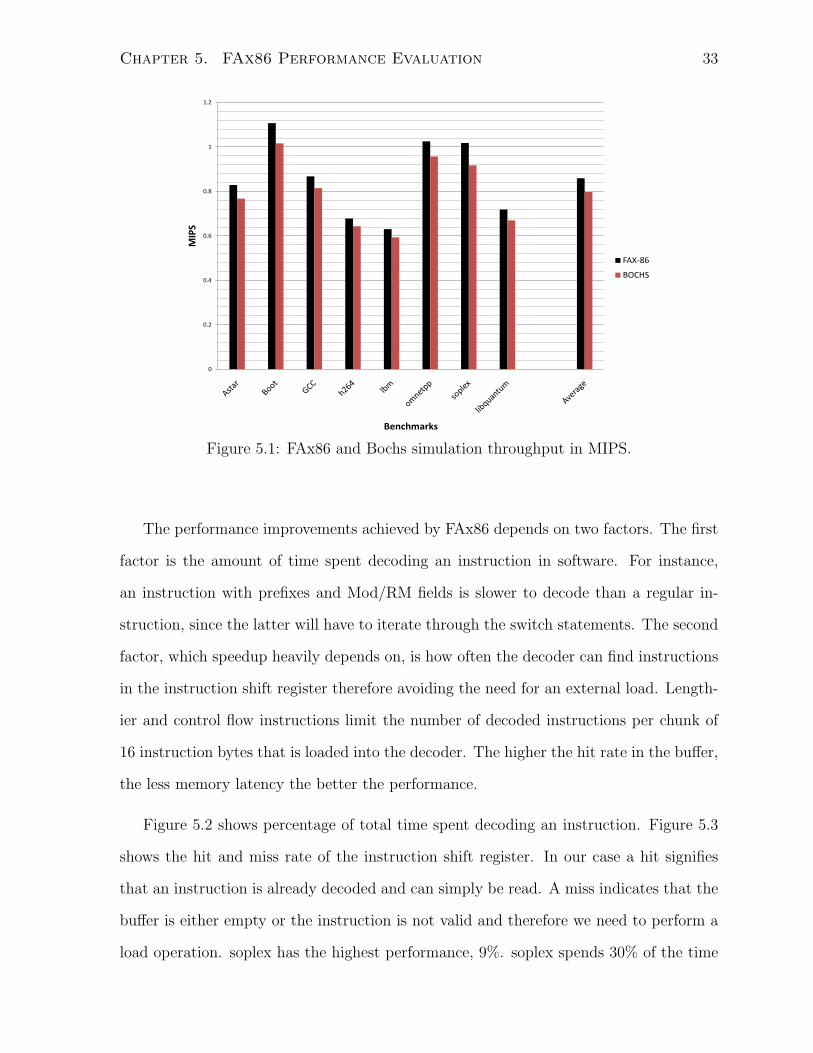
Figure 5.1 reports simulation speed in million instructions per second (MIPS). The right-
most bars represent the stand-alone bochs running on the PowerPC while the left-most
bars represent Bochs coupled with the hardware decoder. The default Bochs configura-
tion achieves an average simulation speed of 0.78 MIPS as opposed to 0.86 for FAx86.
Performance improvements with FAx86 vary from as low as 5% (lbm, h264) to as high
as 9% (soplex). FAx86 accelerates Linux boot simulation by 8%.
Chapter 5. FAx86 Performance Evaluation 33
0
0.2
0.4
0.6
0.8
1
1.2
MIPS
Benchmarks
FAX-86
BOCHS
Figure 5.1: FAx86 and Bochs simulation throughput in MIPS.
The performance improvements achieved by FAx86 depends on two factors. The first
factor is the amount of time spent decoding an instruction in software. For instance,
an instruction with prefixes and Mod/RM fields is slower to decode than a regular in-
struction, since the latter will have to iterate through the switch statements. The second
factor, which speedup heavily depends on, is how often the decoder can find instructions
in the instruction shift register therefore avoiding the need for an external load. Length-
ier and control flow instructions limit the number of decoded instructions per chunk of
16 instruction bytes that is loaded into the decoder. The higher the hit rate in the buffer,
the less memory latency the better the performance.
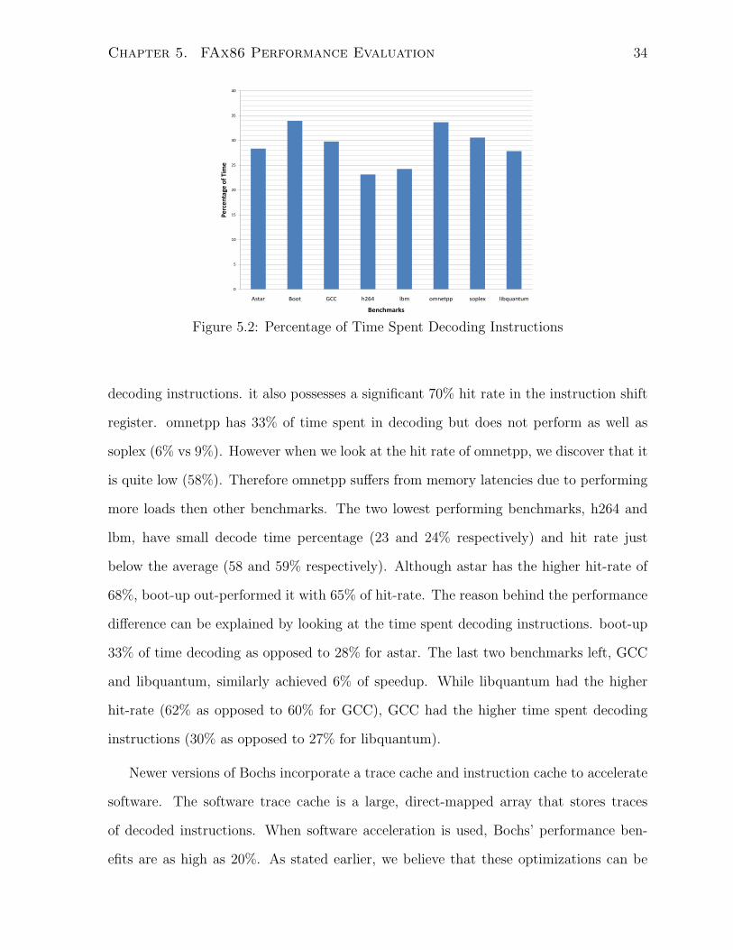
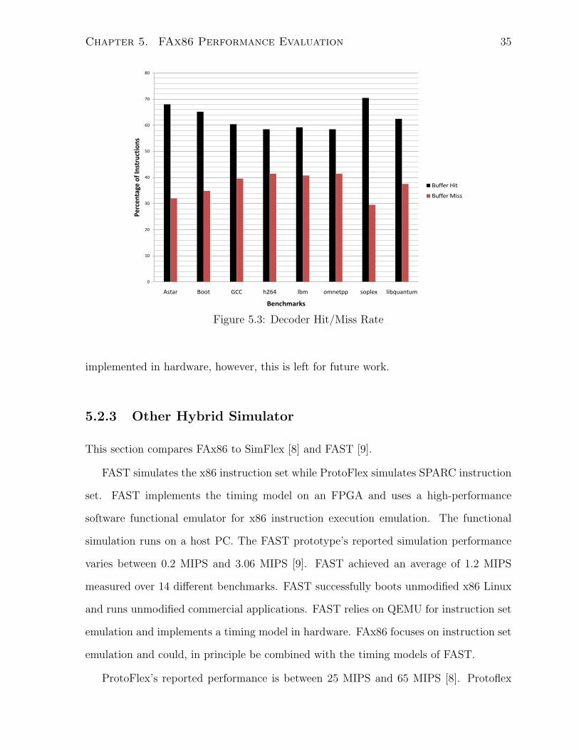
Figure 5.2 shows percentage of total time spent decoding an instruction. Figure 5.3
shows the hit and miss rate of the instruction shift register. In our case a hit signifies
that an instruction is already decoded and can simply be read. A miss indicates that the
buffer is either empty or the instruction is not valid and therefore we need to perform a
load operation. soplex has the highest performance, 9%. soplex spends 30% of the time
Chapter 5. FAx86 Performance Evaluation 34
0
5
10
15
20
25
30
35
40
Astar Boot GCC h264 lbm omnetpp soplex libquantum
Perc
enta
ge o
f Ti
me
Benchmarks
Figure 5.2: Percentage of Time Spent Decoding Instructions
decoding instructions. it also possesses a significant 70% hit rate in the instruction shift
register. omnetpp has 33% of time spent in decoding but does not perform as well as
soplex (6% vs 9%). However when we look at the hit rate of omnetpp, we discover that it
is quite low (58%). Therefore omnetpp suffers from memory latencies due to performing
more loads then other benchmarks. The two lowest performing benchmarks, h264 and
lbm, have small decode time percentage (23 and 24% respectively) and hit rate just
below the average (58 and 59% respectively). Although astar has the higher hit-rate of
68%, boot-up out-performed it with 65% of hit-rate. The reason behind the performance
difference can be explained by looking at the time spent decoding instructions. boot-up
33% of time decoding as opposed to 28% for astar. The last two benchmarks left, GCC
and libquantum, similarly achieved 6% of speedup. While libquantum had the higher
hit-rate (62% as opposed to 60% for GCC), GCC had the higher time spent decoding
instructions (30% as opposed to 27% for libquantum).
Newer versions of Bochs incorporate a trace cache and instruction cache to accelerate
software. The software trace cache is a large, direct-mapped array that stores traces
of decoded instructions. When software acceleration is used, Bochs’ performance ben-
efits are as high as 20%. As stated earlier, we believe that these optimizations can be
Chapter 5. FAx86 Performance Evaluation 35
0
10
20
30
40
50
60
70
80
Astar Boot GCC h264 lbm omnetpp soplex libquantum
Perc
enta
ge o
f In
stru
ctio
ns
Benchmarks
Buffer Hit
Buffer Miss
Figure 5.3: Decoder Hit/Miss Rate
implemented in hardware, however, this is left for future work.
5.2.3 Other Hybrid Simulator
This section compares FAx86 to SimFlex [8] and FAST [9].
FAST simulates the x86 instruction set while ProtoFlex simulates SPARC instruction
set. FAST implements the timing model on an FPGA and uses a high-performance
software functional emulator for x86 instruction execution emulation. The functional
simulation runs on a host PC. The FAST prototype’s reported simulation performance
varies between 0.2 MIPS and 3.06 MIPS [9]. FAST achieved an average of 1.2 MIPS
measured over 14 different benchmarks. FAST successfully boots unmodified x86 Linux
and runs unmodified commercial applications. FAST relies on QEMU for instruction set
emulation and implements a timing model in hardware. FAx86 focuses on instruction set
emulation and could, in principle be combined with the timing models of FAST.
ProtoFlex’s reported performance is between 25 MIPS and 65 MIPS [8]. Protoflex
Chapter 5. FAx86 Performance Evaluation 36
directly runs most SPARC instructions using the BlueSPARC soft core. BlueSPARC
executes the most common and simple instructions of the UltraSPARC-III. Other in-
structions are simulated in software. ProtoFlex relies on a closed-source tool, Simics, for
full-system emulation and does not emulate floating-point instructions in hardware. A
slow link is used with the Simics host. I/O operations have to be simulated and commu-
nicated over this link. BlueSPARC has an interleaved pipeline where each pipeline stage
processes an instruction coming from a different emulated processor. Like ProtoFlex,
FAx86 requires few hardware resources and can easily be ported to soft processors. There-
fore we can simply replicate the hardware when simulating multiple processors. Similar
to ProtoFlex, FAx86’s decoder is designed so that it can be interleaved among multiple
emulated processors. FAx86 follows a similar design philosophy trying to implement in
hardware the most common operations. Unlike a load/store architecture like SPARC,
the most time consuming part of x86 instruction emulation is instruction decoding. Fol-
lowing ProtoFlex’s design philosophy, the next steps in developing FAx86 are to move
part of instruction execution in hardware.
Chapter 6
Conclusion
6.1 Summary
FAx86, an open-source hybrid IA-32 full-system simulator based on the Bochs software
simulator was presented. Since Bochs spends a significant portion of runtime decoding
instructions, a hardware decoder accelerator was designed. The accelerator is designed
as a plug-in replacement for the software decoder. The bulk of the decoder however can
be used in a design that moves other parts of the simulation into hardware. The decoder
is fully-pipelined, can be multiplexed over multiple simulated cores, and operates at 200
MHz. The FAx86 simulator improved simulation over the base software implementation
by 5% to 9%. FAx86 is implemented over a single Virtex-5 FPGA and occupies only a
small fraction of the chip.
Given the low cost of the hardware decoder we believe that it can be used as a
building block for many-core simulators offering higher performance improvement over
software-only simulators. Our hope is that FAx86 will serve as the basis upon which such
simulators can be developed. To the best of our knowledge this is the first hybrid x86
simulator that is open source and that implements x86 decoding in hardware.
37
Chapter 6. Conclusion 38
6.2 Future work
Future work may focus on porting parts of the x86 instruction execution onto hardware,
thus creating a x86 datapath that supports the most common and simple x86 instructions.
The software will then be responsible to emulate complex instructions that are otherwise
hard to implement in FPGA fabric. Although the infrastructure will remain the same, a
Direct Memory Access (DMA) unit will be added to reduce traffic between the software
and hardware when simulating multi-core systems, resulting in a higher performance.
An alternative path to a x86 datapath, would be to re-design the hardware decoder to
produce micro-ops. However, a complete redesign of the software-simulator would be
needed. Even in this case, FAx86 would serve as a basis for comparison.
FAx86 will be made available as an open-source distribution as of February 2011 on
our website at http://www.eecg.toronto.edu/ ferzliel/FAx86
Bibliography
[1] Darek Mihocka and Stansilav Shwartsman. Virtualization without direct
execution or jitting: Designing a portable virtual machine infrastructure.
http://bochs.sourceforge.net/Virtualization Without Hardware Final.pdf.
[2] Intel 64 and ia-32 architectures software developer’s manual: Volumes 2a-2b, in-
struction set reference. http://www.intel.com/products/processor/manuals/, June
2009.
[3] Kevin Lawton. Bochs: The cross platform ia-32 emulator.
http://bochs.sourceforge.net/, 2001-2009.
[4] Peter S. Magnusson, Magnus Christensson, Jesper Eskilson, Daniel Forsgren, Gustav
Hallberg, Johan Hogberg, Fredrik Larsson, Andreas Moestedt, and Bengt Werner.
Simics: A full system simulation platform. Computer, 35(2):50–58, 2002.
[5] Matt T. Yourst. Ptlsim users guide and reference: The anatomy of an x86-64 out of
order superscalar microprocessor. http://www.ptlsim.org/index.php, 2003-2009.
[6] Fabrice Bellard. Qemu, a fast and portable dynamic translator. USENIX Annual
Technical Conference (ATEC05), 2005.
[7] Thomas F. Wenisch, Roland E. Wunderlich, Mike Ferdman, Anastassia Ailamaki,
Babak Falsafi, and James C. Hoe. Simflex: Statistical sampling of computer archi-
39
Bibliography 40
tecture simulation. IEEE Micro special issue on Computer Architecture Simulation,
July/August 2006.
[8] Eric S. Chung, Michael K. Papamichael, Eriko Nurvitadhi, James C. Hoe, Ken
Mai, and Babak Falsafi. Protoflex: Towards scalable, full-system multiprocessor
simulations using fpgas. ACM Trans. Reconfigurable Technol. Syst., 2(2):1–32, 2009.
[9] Derek Chiou, Dam Sunwoo, Joonsoo Kim, Nikhil Patil, William H. Reinhart, D. Eric
Johnson, and Zheng Xu. The fast methodology for high-speed soc/computer simu-
lation. Proceedings of International Conference on Computer-Aided Design ICCAD,
2007.
[10] Michael Pellauer, Muralidaran Vijayaraghavan, Michael Adler, Arvind, and Joel
Emer. Quick performance models quickly: Closely-coupled partitioned simulation
on fpgas. IEEE International Symposium on Performance Analysis of Systems and
Software (ISPASS), 2008.
[11] Alex Krasnov, Andrew Schultz, John Wawrzynek, Greg Gibeling, and Pierre-Yves
Droz. Ramp blue: A message-passing manycore system in fpgas. International
Conference on Field Programmable Logic and Applications, 2007.
[12] Sewook Wee, Jared Casper, Njuguna Njoroge, Yuriy Tesylar, Daxia Ge, Christos
Kozyrakis, and Kunle Olukotun. A practical fpga-based framework for novel cmp
research. Proceedings of the 2007 ACM/SIGDA 15th international symposium on
Field programmable gate arrays, 2007.
[13] Zhangxi Tan, Andrew Waterman, Henry Cook, Sarah Bird, Krste Asanovic, and
David Patterson. A case for fame: Fpga architecture model execution. Proceedings
of the 37th annual international symposium on Computer architecture ISCA2010,
2010.
Bibliography 41
[14] Embedded processor block in virtex-5 fpgas reference guide.
http://www.xilinx.com/support/ documentation/user guides/ug200.pdf, Jan-
uary 2009.
[15] Ahmad Ansari, Peter Ryser, and Dan Isaacs. Embedded processor block in virtex-
5 fpgas reference guide. http://www.xilinx.com/publications/xcellonline/xcell
52/xc pdf/xc v4acu52.pdf, 2005.
[16] Microblaze processor reference guide. http://www.xilinx.com/support/documentation/sw manualsmb ref guide.pdf,
2008.