Embed Size (px)
Citation preview

ADMA_27_46_cover.indd 5 17/11/15 4:10 AM
© 2014 WILEY-VCH Verlag GmbH & Co. KGaA, Weinheim7552 wileyonlinelibrary.com
REV
IEW Exploring the Potential of Nucleic Acid Bases in Organic
Light Emitting Diodes
Eliot F. Gomez , Vishak Venkatraman , James G. Grote , and Andrew J. Steckl*
DOI: 10.1002/adma.201403532
1. Introduction
Natural electronics (or bioelectronics) is a rising fi eld of research that seeks to use biological materials in micro- and opto-elec-tronic organic devices. [ 1–4 ] There are many opportunities to explore since nature supplies a practically limitless library of biological materials (biomaterials) that are renewable, inexpen-sive, ecologically safe, and with fi ne-tuned properties for poten-tial applications in electronic devices. Natural electronics have the ultimate intention of creating “green electronics” that are
Naturally occurring biomolecules have increasingly found applications in organic electronics as a low cost, performance-enhancing, environmentally safe alternative. Previous devices, which incorporated DNA in organic light emitting diodes (OLEDs), resulted in signifi cant improvements in perfor-mance. In this work, nucleobases (NBs), constituents of DNA and RNA polymers, are investigated for integration into OLEDs. NB small molecules form excellent thin fi lms by low-temperature evaporation, enabling seam-less integration into vacuum deposited OLED fabrication. Thin fi lm proper-ties of adenine ( A ), guanine ( G ), cytosine ( C ), thymine ( T ), and uracil ( U ) are investigated. Next, their incorporation as electron-blocking (EBL) and hole-blocking layers (HBL) in phosphorescent OLEDs is explored. NBs affect OLED performance through charge transport control, following their elec-tron affi nity trend: G < A < C < T < U . G and A have lower electron affi nity (1.8–2.2 eV), blocking electrons but allowing hole transport. C , T , and U have higher electron affi nities (2.6–3.0 eV), transporting electrons and blocking hole transport. A -EBL-based OLEDs achieve current and external quantum effi ciencies of 52 cd A −1 and 14.3%, a ca. 50% performance increase over the baseline device with conventional EBL. The combination of enhanced perfor-mance, wide diversity of material properties, simplicity of use, and reduced cost indicate the promise of nucleobases for future OLED development.
environmentally responsible and biode-gradable for sustainability. [ 5 ] Additionally, biomaterials typically originate from rela-tively inexpensive and plentiful sources inspiring low-cost, high-volume, and dis-posable electronic applications. Biomate-rials have intrinsic order and functionality that may offer unique properties and abilities that can lead to enhanced device performance. The list of organic bioma-terials for natural electronics continues to grow: natural dyes, [ 6,7 ] proteins, [ 8,9 ] rubber, [ 10 ] silk, [ 11,12 ] aloe vera, [ 13 ] plant cel-lulose, [ 14 ] common comestibles, [ 15 ] mel-anin, [ 16 ] and nucleic acids. [ 17,18 ] DNA has been investigated for a diverse set of bio-electronic and biophotonic devices within the last decade due to its opto-electronic properties and natural abundance. Nat-ural DNA is a renewable resource har-vested from a variety of animal and plant sources, including salmon sperm, [ 19 ] calf thymus, [ 20 ] and vegetation [ 21 ] .
After harvesting and purifi cation, DNA takes the form of a fi brous powder mate-rial. Next, the DNA is typically bound to a cationic surfactant, such as cetyltri-
methylammonium chloride (CTAC), which requires several processing steps prior to thin-fi lm device fabrication. [ 22 ] The resulting DNA–cetyltrimethylammonium (CTMA) complex is not water soluble but is soluble in alcohols and can form high-quality thin fi lms by spin coating. DNA–CTMA fi lms inserted in fl uorescent [ 23 ] and phosphorescent organic light emit-ting diodes (OLED) [ 24 ] have resulted in signifi cant increases in device performance. The improvement in OLED perfor-mance was attributed to the small electron affi nity (0.9–1.6 eV, reported values vary depending on measurement technique, see Section 2.3) and large energy gap (ca. 4.0–4.7 eV) of DNA between the highest occupied molecular orbital (HOMO) and the lowest unoccupied molecular orbital (LUMO). These prop-erties result in controlled electron fl ow and improved exciton recombination effi ciency, resulting in high emission effi ciency and luminance levels.
The famous DNA double helix structure [ 25 ] contains unique sequences of paired hydrogen-bonded nitrogenous bases stacked between two sugar–phosphate backbones, as illustrated in Figure 1 , that hold the genetic code of all living organisms. The nucleobases (NB) of the DNA, also called nucleic acid bases,
E. F. Gomez, V. Venkatraman, Dr. A. J. Steckl Nanoelectronics Laboratory University of Cincinnati Cincinnati , OH 45221–0030 , USA E-mail: [email protected] Dr. J. G. Grote Air Force Research Laboratory Wright-Patterson Air Force Base OH 45433–7707 , USA
Adv. Mater. 2015, 27, 7552–7562
www.advmat.dewww.MaterialsViews.com

7553wileyonlinelibrary.com© 2014 WILEY-VCH Verlag GmbH & Co. KGaA, Weinheim
REV
IEW
or simply bases, are adenine ( A ), guanine ( G ), cytosine ( C ), and thymine ( T ). RNA is a single-stranded nucleic acid polymer that has the critical task of transcribing the DNA base sequence into various proteins. RNA contains A , C , G , and uracil ( U ) bases. NBs can be extracted from renewable materials or created syn-thetically [ 26,27 ] making them a signifi cantly cheaper alternative to traditional organic optoelectronic materials and DNA. The NBs are small molecules that vacuum vapor deposit without requiring further modifi cation for device fabrication.
NBs have similar HOMO–LUMO energy gaps (ranging from ca. 3.6 to 4.1 eV, see further discussion in Section 2.3) as DNA, but a fairly large range of electron affi nity values (1.8–3.0 eV) that allow an additional degree of freedom in device design. In addition, NBs are small molecules with a simpler structure and much lower molecular weight than that of DNA polymers, which makes them much easier to use and more reproducible in terms of their properties.
There have been many examples of biomaterials in natural electronics within the last decade, many of them catalogued by Meredith [ 4 ] and Irimia-Vladu et al. [ 2 ] Here, we briefl y sum-marize the diverse impact that specifi cally nucleic acids (DNA and NBs) have had in natural electronics. Table 1 summarizes highlights of devices that have incorporated nucleic acids. In 2006, DNA was incorporated as an electron-blocking/hole-trans-porting layer (EBL/HTL) in OLEDs by Hagen et al. to improve the current effi ciency and luminance over the fl uorescent base-line. [ 23 ] The results of the DNA as an EBL/HTL were repeated in other similar OLEDs including fl uorescent, [ 28,29 ] polymer, [ 30–32 ] quantum dot, [ 33 ] and phosphorescent OLEDs [ 24,34 ] all showing a similar increase in performance. Another applications was a color-tunable OLED that used a DNA complex [DNA/polyaniline/Ru(bpy) 3 2+ ] to shift recombination to different emission layers as the electric fi eld increased. [ 35 ] More recently, DNA was imple-mented as a triplet host material in a phosphorescent device to improve electron transport and luminance. [ 36 ] In work apart from OLEDs, DNA has appeared in many different types of opto/electro nic devices. It has been successfully employed as a gate dielectric layer in organic fi eld-effect transistors (OFETs) [ 37–39 ] and it was explored as a charge injection layer in OFETs resulting in a 3–4× increase in effective mobility by reducing the contact resistance. [ 40 ] Other notable work with DNA includes: organic photovoltaic (OPV) devices, [ 41,42 ] lasers, [ 43 ] memory devices, [ 44,45 ] waveguides, [ 46 ] capacitors, [ 47 ] and solid-state lighting. [ 48 ]
NBs are simpler molecules, but surprisingly there have been far fewer reports of NBs incorporated in natural electronics. Early work for NBs in this direction began circa 2003. The NB derivative deoxyguanosine, a single-stranded DNA with only G in the base sequence, was used as a self-assembled p-channel for OFETs. [ 52 ] In 2010, Irimia-Vladu et al. deposited A and G as a dielectric in an OFET made entirely with all-natural mate-rials. [ 15 ] Shi et al. published work regarding G as a charge injec-tion layer in a pentacene OFET. [ 51 ] Most recently, Lee et al. have characterized and implemented G [ 53 ] in the dielectric layer as a hydrogen getter and charge trap layer for improved stability and nonvolatile photo memory. [ 50 ] All of this notable work on NBs has focused entirely on OFETs, but there has been little effort to expand the list of natural materials available for OLEDs beyond DNA. NBs are an excellent choice since they build on the ear-lier work with DNA and offer a diverse range of properties.
Eliot F. Gomez received his B.S. degree in 2009 and is currently pursing a Ph.D. in Electrical Engineering at the University of Cincinnati in Ohio. His doctoral study at the Nanoelectronics Laboratory, in collaboration with the Wright-Patterson Air Force Research Laboratory, focuses on using biomolecules and natural materials in OLEDs.
James G. Grote is Principal Electronics Research Engineer for the Air Force Research Laboratory (AFRL), Materials Directorate. He conducts research in biotronics, biopolymer materials, and devices for photonic, opto/electronic appli-cations. He is an AFRL, SPIE, OSA, and EOS Fellow and an IEEE Senior Member. He is recipient of the ASC Research Achievement Award, IEEE
Dayton Section Russ Bio-Engineering Award, SPIE Technology Achievement Award, Doctor Honoris Causa Politehnica University of Bucharest and Inductee, Ohio University Russ College of Engineering Academy of Distinguished Graduates.
Andrew J. Steckl is Distinguished Research Professor, Gieringer Chair Professor and Ohio Emi-nent Scholar at the University of Cincinnati. Current research activities in his NanoLab group include organic light emitting diodes, microfl uidic devices for Lab-on-Chip applications, and nanofi ber formation by elec-trospinning for chem/bio/med
applications. He is a Fellow of AAAS and Life Fellow of IEEE. In 2006 he received the Rieveschl Award for Distinguished Scientifi c Research at the University of Cincinnati.
In previous work, we reported the results of high effi ciency OLEDs using A and T as electron-blocking layers. [ 49 ] In this work, we expand the investigation to all the NBs, as both electron-blocking layers (EBL) and hole-blocking layers (HBL), along with their related thin fi lm properties. A phosphores-cent Ir(ppy) 3 OLED (PhOLED) device previously employed in the DNA bio-OLEDs study [ 24 ] was also used here. Each NB was investigated as both an EBL and an HBL in the OLED structure. The NB-OLEDs were compared to DNA-OLEDs, which used spin coated DNA–CTMA as an EBL. The OLED results show that purines ( A and G) are suitable EBL/HTL materials, while the pyrimidines ( C , T , and U ) are useful as hole blocking/elec-tron transport (HBL/ETL) materials.
Adv. Mater. 2015, 27, 7552–7562
www.advmat.dewww.MaterialsViews.com

7554 wileyonlinelibrary.com © 2014 WILEY-VCH Verlag GmbH & Co. KGaA, Weinheim
REV
IEW
2. Thin Film Properties
All fi ve NBs were received in the form of white powders (Sigma–Aldrich) and used without any further purifi cation. The purity of the bases was ≥99% except for guanine, which was available at 98% purity. NBs were individually evaporated using an ultrahigh vacuum (10 −8 Torr) molecular beam depo-sition (MBD) system (SVT Associates) onto quartz and silicon substrates. Films were deposited at a rate of ca. 0.1 nm s −1 up to a thickness of ca. 100 nm.
2.1. Optical Properties
Optical transmission spectra of NB thin fi lms deposited on quartz substrates were measured (Perkin–Elmer Lambda 900) over the wavelength range of 200–900 nm. Refractive index and fi lm thickness on silicon were obtained with ellipsometry (J.A. Woollam Co. VASE). All of the NB fi lms, including DNA–CTMA thin fi lms, show absorption peaks in the near-UV and are transparent in the visible and near IR spectrum (400–900 nm). The spectra shown in Figure 2 contain distinctive UV absorp-tion peaks, which correlate well with reported values for cor-responding aqueous solution. [ 54 ]
2.2. Thermogravimetric Analysis
Thermogravimetric analysis (TGA) was performed (Netzsch STA 409 PC Luxx) to determine the thermal stability (physical or chemical changes) of the NBs and related materials. All samples were in powder form consisting of 10 mg. The temperature was increased from 30 °C to 550 °C at a rate of 10 °C min −1 in an
Ar atmosphere. The temperature stability is defi ned here as the point of 5% decrease of the original mass except in those cases where water retention (and removal) is apparent. As shown in Figure 3 , the two pyrimidines T and U display nearly equal thermal stability points of 260 and 270 °C, respectively, after which they rapidly lose mass and are completely evap-orated at ca. 350 °C. Interestingly, the purine A has a very similar trend with only slightly higher stability point of 290 °C and complete evaporation temperatures of 360 °C. C has a higher thermal stability point of 325 °C. At higher temperatures, the C sample loses mass rapidly until it reaches ca. 60% remaining mass at ca. 340 °C. Beyond this temperature, the mass loss for the C sample occurs much more gradually (unlike the other pyrimidines), indicating carbonization of the sample. At the highest measurement temperature of 550 °C, approximately 50% of the original mass still remains. Finally, the G sample displays the highest stability temperature of ca. 465 °C. The high thermal stability of G is due to high crystal lattice energy attributed to the presence of oxo and amino groups which encourage intermolecular hydrogen bonding. [ 55 ]
To compare with the bases, TGA was also performed on DNA (200 kDa), adenosine (a nucleoside con-sisting of base sugar groups, but without the phosphate group), adenosine triphosphate (ATP) (base, sugar, and three phos-phate groups), DNA–CTMA, and ATP–CTMA. As shown in Figure 3 b, DNA, DNA–CTMA, ATP, and ATP–CTMA showed a 5–10% decrease in mass as the temperature was ramped up to ca. 150 °C. This is most likely due to water retention in the sample materials. Since DNA showed the greatest early mass loss, the TGA experiment was repeated after vacuum drying the DNA powder for 1 week in high vacuum (10 −7 Torr), producing the same results. These four materials all became thermally unstable between 200 and 220 °C. Adenosine showed no evidence of water retention and became ther-mally unstable at a slightly higher temperature of 280 °C. Upon removal from the TGA system, all the samples, except those that were completely evaporated ( T , U, and A ), were carbonized.
2.3. Dielectric Properties
Lastly, a parallel plate capacitor structure with an active area of 4 mm 2 was fabricated to measure the dielectric constant of the NB fi lms (100 nm) using ITO as the bottom electrode and aluminum as the top electrode. The capacitance was measured (HP4275A LCR meter) at 1 MHz and the dielectric constant was calculated accordingly. These results are slightly lower than those reported in a similar study [ 56 ] of the dielectric con-stant, which however were measured at 1 kHz. A summary of the measured thin fi lm optoelectronic properties is shown in Table 2 .
Adv. Mater. 2015, 27, 7552–7562
www.advmat.dewww.MaterialsViews.com
Figure 1. DNA consists of a double-stranded chain of nucleotide links with each nucleotide composed of a pentose sugar molecule, a phosphate group, and a nucleobase.

7555wileyonlinelibrary.com© 2014 WILEY-VCH Verlag GmbH & Co. KGaA, Weinheim
REV
IEW
2.4. Molecular Orbital Energy Levels
Molecular orbital energy level (HOMO/LUMO) analysis of the NBs has been reported by several groups. [ 53,57–60 ] UV photoemission spectroscopy (UPS) of all the DNA bases has recently been reported [ 50,53 ] by Lee and co-workers on thin fi lm NBs on ITO and Al electrodes, providing insight into purine and pyrimidine electron/hole injection. Faber et al. [ 57 ]
performed orbital computations for all NBs. There are discrep-ancies between various studies for the actual orbital energies of the bases, most likely due to different methods of measure-ments and under different conditions (UPS solid fi lm vs com-putational studies). However, all studies reveal that the relative ionization potentials of the bases follow the trend G < A < C < T < U , such that G has the smallest HOMO (ionization potential) level for good hole transport and LUMO (electronic affi nity) for
Adv. Mater. 2015, 27, 7552–7562
www.advmat.dewww.MaterialsViews.com
Table 1. Summary of nucleic acid molecules in organic electronics.
Device type Nucleic acid material Material function Key results Year Ref.
OLED
A, G EBL/HTL η max = 52 cd A −1 ; L max = 82 000 cd m −2 for A 2014 This work
OLED
C, T, U HBL/ETL η max = 16 cd A −1 ; L max = 4000 for U 2014 This work
OLED
A, T EBL η max = 76 cd A −1 ; L max = 132 000 cd m −2 for T 2014 [49]
OLED
DNA Phosphorescent host Improved electron transport; increased luminance 2010 [36]
OLED
DNA EBL/HTL Color-tunable emission 2010 [35]
OLED
DNA EBL/HTL Increase luminance and current effi ciency 2006–2014 [23,24,28–34]
OFET
G Dielectric Improved stability; V th shift for non-volatile memory 2014 [50]
OFET
DNA, G Charge injection Increase in mobility from 0.02 to 0.104 cm 2 V −1 s −1 with DNA 2014 [51]
OFET
DNA Charge injection 3–4× increase in mobility, reduced contact resistance 2012 [40]
OFET
A, G Dielectric All-natural OFET 2010 [15]
OFET
DNA Dielectric High mobility 0.31 cm 2 V −1 s −1 2010 [37]
OFET
DNA Dielectric Lower operating voltage, reduced hysteresis 2009 [38]
OFET
Deoxyguanosine p-channel Self-assembled; voltage gain of 0.76 2003 [52]
Solid-state lighting
DNA DNA-phosphor blend Enhanced color and luminance for white LEDs 2012 [48]
Memory
DNA Photoactive layer Photo-induced memory read/write, ca. 2.6 V threshold 2011 [44]
Capacitor
DNA Electrode DNA-PEDOT composite, improved capacitive activity 2010 [47]
OPV
DNA EBL Increase in power conversion effi ciency 2008,2011 [41,42]
Laser
DNA Dye host ca. 2× decrease in threshold energy (from 5.1 to 3 µJ) 2007 [43]
Waveguide
DNA Core/cladding Reduced optical loss; n tunable; improved activity 2006 [46]

7556 wileyonlinelibrary.com © 2014 WILEY-VCH Verlag GmbH & Co. KGaA, Weinheim
REV
IEW
Adv. Mater. 2015, 27, 7552–7562
www.advmat.dewww.MaterialsViews.com
Figure 2. Near-ultraviolet absorption as a function of wavelength for thin fi lm samples of the nucleic acid bases and DNA–CTMA; no signifi cant absorption was detected in the visible range. Film thickness ≈ 100 nm.
Figure 3. Thermogravimetric measurements from 30 to 550 °C increased at 10 °C min −1 , indicating the temperature stability range of: a) nucleic acid bases – G , A , C , T , U ; b) DNA, DNA–CTMA, adenosine, ATP, and ATP–CTMA.
Table 2. Thin fi lm properties of thin fi lm nucleobases for OLED.
G A C T U
Refractive index (580 nm) 1.96 1.73 1.76 1.50 1.67
Relative dielectric constant (1 MHz)
ca. 4.0 ca. 3.4 ca. 4.3 ca. 2.0 ca. 1.6
Deposition temp [°C] 340 185 220 180 175
HOMO [eV] [56] 5.7 6.0 6.2 6.5 6.7
LUMO [eV] [56] 1.8 2.2 2.6 2.8 3.0
Molecular orbital gap [eV] 3.9 3.8 3.6 3.7 3.7
Thermal stability [°C] (95% remaining mass)
465 290 325 260 270

7557wileyonlinelibrary.com© 2014 WILEY-VCH Verlag GmbH & Co. KGaA, Weinheim
REV
IEW
electron blocking, while U has the largest LUMO level for good electron transport and HOMO for hole blocking. All the bases have a wide molecular orbital gap of ca. 3.6–4.1 eV. Figure 4 shows a side-by-side comparison of energy levels in the base-line device (Type I) structure and the estimated levels for the NBs. The NB energy levels shown with a solid black line are reported calculations of all of the NBs from Faber et al. [ 57 ] The levels shown with a gray dotted line are measured values from Lee et al. [ 53 ] obtained using UPS measurements on G , A , C , and T thin fi lms. The DNA–CTMA levels were obtained by Lin et al. [ 61 ] using UPS, which have a higher electron affi nity (1.6 eV), are compared to the typical reported electron affi nity (0.9 eV). [ 23 ] Both reports indicate a similar ionization potential of 5.6 eV for DNA–CTMA.
3. OLED Fabrication
The OLED fabrication process started with glass substrates that contained the ITO anode pattern. The ITO/glass sub-strates were cleaned by thoroughly scrubbing with detergent and washing in organic solvents. The substrates were then rinsed with de-ionized water and dried. Next, the substrates were exposed to oxygen plasma (Plasma-Preen, Terra Universal Inc.) at 500 W for 5 min. After cleaning, fi ltered PEDOT:PSS [poly(3,4-ethylenedioxythiophene) doped with poly(4-styrene-sulfonate)] (Clevios P VP AI 4083) was spin-coated onto the glass/ITO substrates at 2000 rpm for 20 s. The PEDOT:PSS fi lm was baked at 120 ºC for 15 min. The samples were then transferred to a multi-source vacuum evaporation system (SVT Associates) for deposition of the organic materials (Lumines-cence Technology Corp. Hsin-Chu, Taiwan), the NBs, and the cathode. All organic layers were deposited sequentially through a shadow mask and then the substrates were briefl y removed from vacuum in order to apply the cathode mask for the LiF Al layer. Deposition of the organic layers was monitored by a quartz crystal microbalance and also separately verifi ed by ellip-sometery, as described in Section 2.1. After the aluminum was deposited, the devices were transferred to a nitrogen-fi lled box for testing.
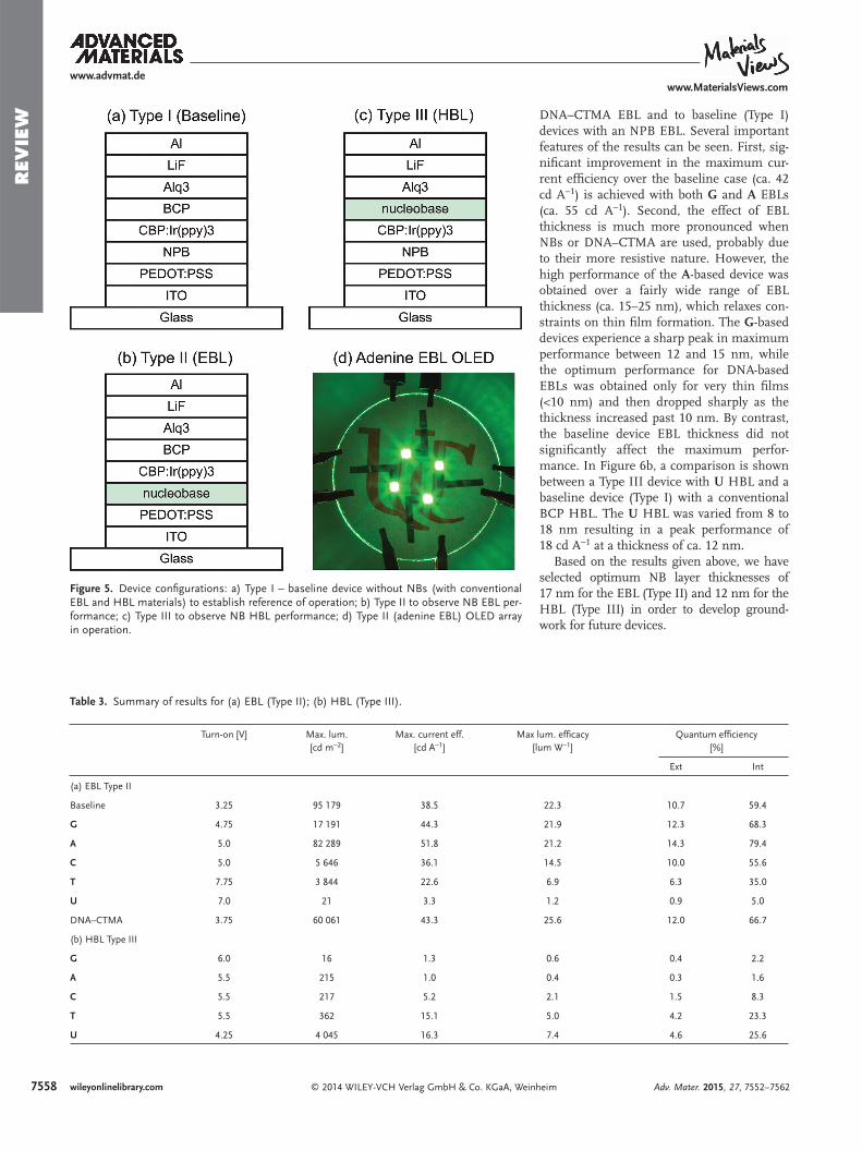
Several structures, shown in Figure 5 , were fabricated to investigate the properties of NB-OLEDs. The standard “baseline” device (Type I) contains no nucleobases or DNA–CTMA. Type II and III devices contain NB layers depos-ited as either an EBL (without NPB) or HBL (without BCP), respectively. A companion baseline device (Type I) was grown with each fabrication run and each device type was fabri-cated several times to ensure consistency and repeatability. Characterization results were then averaged over several runs. The baseline (Type I) structure consisted of the following layer thicknesses: ITO[90 nm]/PEDOT:PSS[40 nm]/NPB[17 nm]/CBP:Ir(ppy) 3 (10 wt%)[30 nm]/BCP[12 nm]/Alq3[25 nm]/LiF[<1 nm]/Al[40 nm]. In the EBL (Type II) confi gura-tion, NPB was replaced by a NB layer: ITO/PEDOT:PSS/NB [17 nm]/CBP:Ir(ppy) 3
(10 wt%)/BCP/Alq3/LiF/Al. In the HBL confi guration (Type III), BCP was replaced by an NB layer: ITO/PEDOT:PSS/NPB/CBP:Ir(ppy) 3 (10 wt%)/NB [12 nm]/Alq3/LiF/Al.
Additionally, a DNA-based OLED was fabricated in the EBL confi guration similar to Type II, except that the DNA–CTMA layer was spin coated while the NB layers were formed by evap-oration. DNA (200 kDa) was complexed with CTAC and the resulting DNA–CTMA was dissolved in butanol at 0.25 wt% (for 8 nm) and 0.5 wt% (for 16 nm) and mixed overnight. After the PEDOT:PSS baking step, DNA–CTMA solution was spin coated on top of the PEDOT:PSS layer at 6000 rpm for 20 s and allowed to air dry for 10 min. The device was then transferred to the evaporation system for the deposition of the remaining layers of Type II.
4. OLED Characterization
OLED current–voltage ( I–V ) characterization was performed (HP-6634B DC power source) at 0.25 V intervals and the lumi-nance was measured using a Konica-Minolta CS-200 lumi-nance meter controlled by LabView. The subsequent sections discuss the performance of NB-containing OLEDs of type Type II (EBL) and Type III (HBL). The results show that the purines G and A perform well as an EBL and were able to match or exceed the effi ciency of the baseline (NPB). The pyrimidines C , T , and U block hole transport and are ineffective as an EBL and HTL. The results in Table 3 summarize the peak performance of each device. External quantum effi ciency was calculated according to methods found in literature. [ 63 ] Internal quantum effi ciency is calculated using the external quantum effi ciency divided by the out-coupling factor, assumed to be ca. 18%, based [ 64,65 ] on the critical angle of total internal refl ection within the device.
G , A , and DNA–CTMA layers were varied in thickness to optimize the EBL operation for Type II devices, while U was varied to optimize the HBL operation for Type III devices. The OLED performance was found to be very sensitive to the NB thickness, as shown in Figure 6 . In Figure 6 a, results from Type II devices with G and A EBLs are compared to devices with a
Adv. Mater. 2015, 27, 7552–7562
www.advmat.dewww.MaterialsViews.com
Figure 4. Molecular orbital energy levels of the NBs in three different studies compared with levels in the Baseline Type I. Energy levels for G , A , C , T , and U obtained by Faber et al. [ 57 ] are shown as black solid lines (—) and are compared with results from Lee and co-workers [ 50,53 ] (···) where available. The DNA–CTMA energy level from Lin et al. [ 61 ] performed by UPS gives an electron affi nity of 1.6 eV compared with the typical reported value 0.9 eV. [ 23 ] Energy levels of Type I baseline OLED were obtained from Baldo et al. [ 62 ]
7558 wileyonlinelibrary.com © 2014 WILEY-VCH Verlag GmbH & Co. KGaA, Weinheim
REV
IEW DNA–CTMA EBL and to baseline (Type I)
devices with an NPB EBL. Several important features of the results can be seen. First, sig-nifi cant improvement in the maximum cur-rent effi ciency over the baseline case (ca. 42 cd A −1 ) is achieved with both G and A EBLs (ca. 55 cd A −1 ). Second, the effect of EBL thickness is much more pronounced when NBs or DNA–CTMA are used, probably due to their more resistive nature. However, the high performance of the A -based device was obtained over a fairly wide range of EBL thickness (ca. 15–25 nm), which relaxes con-straints on thin fi lm formation. The G -based devices experience a sharp peak in maximum performance between 12 and 15 nm, while the optimum performance for DNA-based EBLs was obtained only for very thin fi lms (<10 nm) and then dropped sharply as the thickness increased past 10 nm. By contrast, the baseline device EBL thickness did not signifi cantly affect the maximum perfor-mance. In Figure 6 b, a comparison is shown between a Type III device with U HBL and a baseline device (Type I) with a conventional BCP HBL. The U HBL was varied from 8 to 18 nm resulting in a peak performance of 18 cd A −1 at a thickness of ca. 12 nm.
Based on the results given above, we have selected optimum NB layer thicknesses of 17 nm for the EBL (Type II) and 12 nm for the HBL (Type III) in order to develop ground-work for future devices.
Adv. Mater. 2015, 27, 7552–7562
www.advmat.dewww.MaterialsViews.com
Figure 5. Device confi gurations: a) Type I – baseline device without NBs (with conventional EBL and HBL materials) to establish reference of operation; b) Type II to observe NB EBL per-formance; c) Type III to observe NB HBL performance; d) Type II (adenine EBL) OLED array in operation.
Table 3. Summary of results for (a) EBL (Type II); (b) HBL (Type III).
Turn-on [V] Max. lum. [cd m −2 ]
Max. current eff. [cd A −1 ]
Max lum. effi cacy [lum W −1 ]
Quantum effi ciency [%]
Ext Int
(a) EBL Type II
Baseline 3.25 95 179 38.5 22.3 10.7 59.4
G 4.75 17 191 44.3 21.9 12.3 68.3
A 5.0 82 289 51.8 21.2 14.3 79.4
C 5.0 5 646 36.1 14.5 10.0 55.6
T 7.75 3 844 22.6 6.9 6.3 35.0
U 7.0 21 3.3 1.2 0.9 5.0
DNA–CTMA 3.75 60 061 43.3 25.6 12.0 66.7
(b) HBL Type III
G 6.0 16 1.3 0.6 0.4 2.2
A 5.5 215 1.0 0.4 0.3 1.6
C 5.5 217 5.2 2.1 1.5 8.3
T 5.5 362 15.1 5.0 4.2 23.3
U 4.25 4 045 16.3 7.4 4.6 25.6

7559wileyonlinelibrary.com© 2014 WILEY-VCH Verlag GmbH & Co. KGaA, Weinheim
REV
IEW
4.1. Nucleobases as Electron-Blocking/Hole-Transport Layer
Figure 7 contains the characteristics of Type II devices with a 17 nm EBL/HTL for each NB: current density (Figure 7 a), luminance (Figure 7 b), luminous effi cacy (Figure 7 c), and cur-rent effi ciency (Figure 7 d). The current (and current density) decreases sequentially in the G , A , C , T , and U trend as predicted by the HOMO/LUMO levels. As shown in Figure 7 a, the G -based device has the largest current and the U -based device the lowest, consistent with the fact that the U HOMO level is largest of all NBs and impedes hole transport the most (see Figure 4 ). While U as an EBL does not lead to functional OLEDs, it shows poten-tial as an ETL/HBL (further discussed in Section 4.2).
The baseline device exhibited an emission turn-on voltage of 3.25 V, as shown in Figure 7 b. G and A devices turned on at 4.75 and 5.0 V, respectively, indicating diminished hole injec-tion and transport at lower voltages, and obtained a maximum luminance of 17 191 and 82 289 cd m −2 , respectively. Although G was a more effi cient HTL than A , as seen by the higher cur-rent in Figure 7 a, current effi ciency in the G -based device expe-rienced an earlier and more pronounced roll-off than that in the A -based device as seen in Figure 7 d. Possible explanations for the reduced performance of the G -based device include the effects of higher refractive index or recombination shifted
away from the emitting layer. The A -based OLED has the highest luminance of the NB-based OLEDs indicating a more favorable transport of holes into the emitting layer. The higher emission turn-on voltage is probably due to poor injection
Adv. Mater. 2015, 27, 7552–7562
www.advmat.dewww.MaterialsViews.com
Figure 6. Effect of nucleobase fi lm thickness on maximum observed OLED current effi ciency: a) EBL thickness in Type II devices with G , A , and DNA–CTMA compared to Type I (Baseline) Device with NPB EBL; b) HBL thickness in U -based Type II devices compared to Type I (Base-line) Device with BCP EBL.
Figure 7. The performance of Type II (NB EBL/HTL) at 17 nm where NB energy levels affect OLED performance: a) current density versus voltage; b) luminance versus voltage; c) luminous effi cacy versus current density; and d) current effi ciency versus luminance.

7560 wileyonlinelibrary.com © 2014 WILEY-VCH Verlag GmbH & Co. KGaA, Weinheim
REV
IEW from the PEDOT:PSS layer, which has a large difference in
HOMO energy levels with the A layer. For the pyrimidines, the C -based OLED turned on at 5.0 V which is similar to the purine-based devices, but its maximum luminance was rather low at 5646 cd m −2 . The T -based device turned on at a signifi -cantly higher voltage (7.75 V) and was only able to reach a lumi-nance of 3844 cd m −2 . Finally, using U as an EBL/HTL barely generated any measurable luminance.
The A -based device displayed the best performance of the NB-based OLEDs and equaled or exceeded the performance of the baseline device. As seen in Figure 7 c, while the A device produced a slightly lower maximum luminous effi cacy (21.2 lum W −1 ) than that of the baseline device (22 lum W −1 ), it exceeded the effi cacy of the baseline device at all values of the current density except for small values (<0.5 mA cm −2 ). For the current effi ciency (shown in Figure 7 d), the A device exceeded the level of the baseline device for a wide range of luminance values (10 2 –10 5 cd m −2 ). The maximum current effi ciency for the A device is 51.8 cd A −1 compared to 38 cd A −1 for the base-line device. The matched HOMO levels of the A layer and the emitting layer provide good hole transport, while the small LUMO level acts as an effi cient electron block. This combina-tion results in an effi cient balance of electrons to holes over the entire range of operating conditions. The G -based device pro-duced the overall second best performance. At low bias voltage, the higher current in the G -based device produces slightly higher luminance than the A -based device. However, at higher voltages the luminance does not increase as quickly as that of the A -based device. The cross-over point is reached at a bias of ca. 11 V, where both devices emit ca. 10 000 cd m −2 . Beyond this point, the emission from the G -based device saturates, reaching a maximum luminance of ca. 17 000 cd m −2 at ca. 14 V. The loss in effi ciency is clearly seen in Figure 7 c and 7 d where the maximum luminous and current effi ciencies of 21.9 lum W −1 and 44.7 cd A −1 , respectively, are achieved at low values of cur-rent density and luminance. The G -based device experiences a much sharper effi ciency roll off than the A -based device. The C -based device reaches relatively high current effi ciencies of 36.1 cd A −1 and 14.5 lum W −1 , just above the emission turn-on. However, the effi ciency roll-off was very pronounced and the device reached a maximum luminance of only ca. 5600 cd m −2 . The current of the C device was only slightly lower than the A device. The T -based device emits only a modest amount of light, with a maximum brightness of ca. 2000 cd m −2 and reaching maximum effi ciencies of only ca. 23 cd A −1 and ca. 7 lum W −1 . Finally, the device with U as an EBL/HTL was not functional.
4.2. Nucleobases as Hole-Blocking/Electron-Transport Layer
Type III devices utilized a 12 nm NB layer in place of the BCP layer to function as an HBL/ETL. The resulting characteristics of Type III devices are presented in Figure 8 . As predicted by the proposed HOMO/LUMO levels, it is not surprising that G and A , which performed well as an EBL/HTL, perform quite poorly as HBL/ETL, with very low luminance and effi ciency. Conversely, C , T , and U, which resulted in mediocre to very poor performance as EBLs, display much better performance as HBLs. All of these results are consistent with the placement
Adv. Mater. 2015, 27, 7552–7562
www.advmat.dewww.MaterialsViews.com
Figure 8. The performance of OLED Type III (NB HBL) at 12 nm: a) cur-rent density versus voltage; b) luminance versus voltage; c) luminous effi -cacy versus current density; and d) current effi ciency versus luminance.

7561wileyonlinelibrary.com© 2014 WILEY-VCH Verlag GmbH & Co. KGaA, Weinheim
REV
IEW
Adv. Mater. 2015, 27, 7552–7562
www.advmat.dewww.MaterialsViews.com
of the HOMO–LUMO levels of the various NBs as HBL/ETL within the energy level diagram of the overall device structure. Clearly, G has an ionization potential that is too small to act as an effi cient hole blocker and an electron affi nity that is too small to allow effi cient injection of electrons. This results in a relatively low current density (Figure 8 a) and very low lumi-nance (Figure 8 b) and emission effi ciencies (Figure 8 c and 8 d). The results of the A device are somewhat puzzling, with a large current density and higher luminance than G . A possible expla-nation might lie in the correct HOMO–LUMO values for A . As seen in Figure 4 , the values reported by Lee et al. [ 53 ] (shown with dashed lines) are signifi cantly larger than the ones reported by Faber et al. [ 57 ] (shown with solid lines). Using the Lee levels, the electron affi nity of A would be larger (2.5 vs 2.2 eV) allowing good electron injection, which would explain the large current density. However, the larger ionization potential reported by Lee should result in an effi cient HBL and hence higher effi ciency, which is not observed.
In this set of NB-based OLEDs, the U -based HBL/ETL displays the highest performance. The high current density (Figure 8 a) and high luminance (Figure 8 b) indicate effi cient electron injection from the cathode, while the fairly high lumi-nous effi cacy (Figure 8 c) and current effi ciency (Figure 8 d) indi-cate balanced charge transport and effi cient recombination due to good hole blocking by the U layer. The relatively early emis-sion turn-on at 4.25 V and high current produced a maximum luminance of ca. 4000 cd m −2 (Figure 8 b) and maximum cur-rent effi ciency of 16 cd A −1 (Figure 8 d). U appears to be prom-ising as an HBL and more careful selection of matching energy levels may produce excellent results. The trend continues in reverse from the NB EBL OLEDs. T was the second best HBL of the NBs. The current was lower than the other NBs, however, the effi ciency was greater with ca. 15 cd A −1 and a maximum luminous effi cacy of 5 lum W −1 . The emission turn-on was at 5.5 V and a maximum luminance of 362 cd m −2 was achieved. C -based HBL has similar current to the T device, but the effi -ciency decreases signifi cantly, indicating a shift to more non-radiative recombination. C only obtains 5.2 cd A −1 and 2.1 lum W −1 . The emission turn-on of the C device was 5.5 V (which is 1.25 V higher than for the U -based device) and a maximum luminance of only 217 cd m −2 was achieved.
5. Summary and Conclusions
OLEDs incorporating thin fi lms of nucleobases as either elec-tron blocking or hole blocking layers have been investigated. The data obtained in this work, in conjunction with the NB HOMO–LUMO energy levels from literature, present a fairly clear understanding of the behavior of the bases in thin-fi lm OLED devices. For the EBL/HTL confi guration (Type II devices), the G -based device has the highest current density, indicating the effect of its ionization potential (smallest among NBs) to induce strong hole injection. The A -based device (with slightly larger electron affi nity and ionization potential) has the most effi cient current transport and emission effi ciency, shifting most of the recombination to the emissive layer over a wide range of voltages. C is in the middle of the NB HOMO–LUMO range and shows both EBL and HBL tendencies. As an EBL,
the C -based device has a somewhat lower current density than A -based device, resulting in lower luminance. However, the decrease in current effi ciency also indicates that the recombina-tion shifts away from the emitting layer. The T - and U -based devices yielded much lower current densities, indicating signif-icant reduction in hole injection due to the increased ionization potential acting as a hole blocker. The U -based EBL device (with the highest ionization potential) basically failed to operate, with an emission in the barely visible level (ca. 10 cd m −2 ).
For the cases where the NBs were inserted as an HBL/ETL (Type III devices), the trend was reversed with respect to the HOMO–LUMO levels. U performed the best of all NBs as an HBL, having the largest current, the best effi ciency, and the highest luminance. T -based Type III device exhibited decreased performance with reductions in current density and luminance. However, the effi ciency remained relatively high indicating fairly strong HBL function. C was once again in the middle, showing both EBL and HBL tendencies. The C -based device had similar current density and luminance as the T -based device. However, its effi ciency was greatly diminished over the entire range, indicating that recombination has partially shifted away from the emitting layer. Finally, A- and G -based devices had suffi cient current den-sity, but their effi ciency was very low. The G -based device only dimly illuminated, reaching ca. 10 cd m −2 at high voltage, similar to the U -based EBL/HTL Type II device. This shows that G is pri-marily an electron blocker and thus not suitable as an HBL/ETL.
We have demonstrated that NBs are a versatile set of molecules for improved OLED performance. NB thin fi lm properties were characterized and were incorporated in a PhOLED device struc-ture as an EBL and HBL. The data presented confi rm that the ion-ization potential for the nucleobases is in the sequence G < A < C < T < U . The purines ( G and A ) with lower ionization poten-tials are suitable as an EBL, while the pyrimidines ( C , T , and U ) with higher ionization potentials are better suited as an HBL. Potential future work includes introducing two NB layers in the OLED as EBL (purines) and HBL (pyrimidines) and investigating other natural material for the HBL. The NBs offer a wide range of functionality in opto/electronic devices, from electron transport to hole transport. This work shows that NBs are attractive bioma-terials that can be readily incorporated by vacuum deposition into OLEDs and possibly other natural electronic applications.
Acknowledgements The authors would like to thank the following: Air Force Research Laboratory for partial support of this work; Dr. Necati Kaval for assistance with ellipsometry and TGA measurements; and Andre Gomez for assisting with DNA artwork and Dr. Han You for assisting with the chemical structures of Figure 1 .
Received: August 3, 2014 Revised: September 24, 2014
Published online: December 12, 2014
[1] M. Irimia-Vladu , N. S. Sariciftci , S. Bauer , J. Mater. Chem. 2011 , 21 , 1350 .
[2] M. Irimia-Vladu , E. D. Głowacki , G. Voss , S. Bauer , N. S. Sariciftci , Mater. Today 2012 , 15 , 340 .

7562 wileyonlinelibrary.com © 2014 WILEY-VCH Verlag GmbH & Co. KGaA, Weinheim
REV
IEW
Adv. Mater. 2015, 27, 7552–7562
www.advmat.dewww.MaterialsViews.com
[3] A. J. Steckl , Nat. Photonics 2007 , 1 , 3 . [4] P. Meredith , C. J. Bettinger , M. Irimia-Vladu , A. B. Mostert ,
P. E. Schwenn , Rep. Prog. Phys. 2013 , 76 , 034501 . [5] M. Irimia-Vladu , Chem. Soc. Rev. 2014 , 43 , 588 . [6] E. D. Głowacki , G. Voss , L. Leonat , M. Irimia-Vladu , S. Bauer ,
N. S. Sariciftci , Isr. J. Chem. 2012 , 52 , 540 . [7] M. Irimia-Vladu , E. D. Głowacki , P. A. Troshin , G. Schwabegger ,
L. Leonat , D. K. Susarova , O. Krystal , M. Ullah , Y. Kanbur , M. A. Bodea , V. F. Razumov , H. Sitter , S. Bauer , N. S. Sariciftci , Adv. Mater. 2012 , 24 , 375 .
[8] N. Solin , O. Inganäs , Isr. J. Chem. 2012 , 52 , 529 . [9] J.-W. Chang , C.-G. Wang , C.-Y. Huang , T.-D. Tsai , T.-F. Guo ,
T.-C. Wen , Adv. Mater. 2011 , 23 , 4077 . [10] P. Predeep , D. Devasia , J. Aneesh , N. M. Faseena , Microelectron.
Eng. 2013 , 107 , 54 . [11] R. Capelli , J. J. Amsden , G. Generali , S. Toffanin , V. Benfenati ,
M. Muccini , D. L. Kaplan , F. G. Omenetto , R. Zamboni , Org. Elec-tron. 2011 , 12 , 1146 .
[12] D.-H. Kim , Y.-S. Kim , J. Amsden , B. Panilaitis , D. L. Kaplan , F. G. Omenetto , M. R. Zakin , J. A. Rogers , Appl. Phys. Lett. 2009 , 95 , 133701 .
[13] L. Q. Khor , K. Y. Cheong , Adv. Mater. Res. 2014 , 858 , 74 . [14] D. Tobjörk , R. Österbacka , Adv. Mater. 2011 , 23 , 1935 . [15] M. Irimia-Vladu , P. A. Troshin , M. Reisinger , L. Shmygleva ,
Y. Kanbur , G. Schwabegger , M. Bodea , R. Schwödiauer , A. Mumyatov , J. W. Fergus , V. F. Razumov , H. Sitter , N. S. Sariciftci , S. Bauer , Adv. Funct. Mater. 2010 , 20 , 4069 .
[16] J. P. Bothma , J. de Boor , U. Divakar , P. E. Schwenn , P. Meredith , Adv. Mater. 2008 , 20 , 3539 .
[17] T. B. Singh , N. S. Sariciftci , J. G. Grote , Adv. Polym. Sci. 2010 , 223 , 73 . [18] Y.-W. Kwon , C. H. Lee , D.-H. Choi , J.-I. Jin , J. Mater. Chem. 2009 , 19 ,
1353 . [19] E. Chargaff , R. Lipshitz , C. Green , M. Hodes , J. Biol. Chem. 1951 ,
192 , 223 . [20] E. Chargaff , C. F. Crampton , R. Lipshitz , Nature 1953 , 172 , 289 . [21] H. B. Zhang , X. Zhao , X. Ding , A. H. Paterson , R. A. Wing , Plant J.
1995 , 7 , 175. [22] E. F. Gomez , H. D. Spaeth , A. J. Steckl , J. G. Grote , presented at
Proc. SPIE 8103, Nanobiosystems: Processing, Characterization, and Applications IV , San Diego, CA, USA , September, 2011 .
[23] J. A. Hagen , W. Li , A. J. Steckl , J. G. Grote , Appl. Phys. Lett. 2006 , 88 , 171109 .
[24] A. J. Steckl , H. Spaeth , H. You , E. Gomez , J. Grote , Opt. Photonics News 2011 , 22 , 34 .
[25] J. D. Watson , F. H. C. Crick , Nature 1953 , 171 , 737 . [26] H. Rosemeyer , Chem. Biodiversity 2004 , 1 , 361 . [27] I. M. Lagoja , Chem. Biodiversity 2005 , 2 , 1 . [28] .I. C. Chen , Y.-W. Chiu , L. Fruk , Y.-C. Hung , presented at Proc IQEC/
CLEO Pacifi c Rim 2011 , Sydney, Australia, August, 2011 . [29] R. B. Gupta , S. Nagpal , S. Arora , P. K. Bhatnagar , P. C. Mathur , J.
Nanophotonics 2011 , 5 , 059505 . [30] Q. Sun , D. W. Chang , L. Dai , J. Grote , R. Naik , Appl. Phys. Lett.
2008 , 92 , 251108 . [31] D. Madhwal , S. S. Rait , A. Verma , A. Kumar , P. K. Bhatnagar ,
P. C. Mathur , M. Onoda , J. Lumin. 2010 , 130 , 331 . [32] P. Zalar , D. Kamkar , R. Naik , F. Ouchen , J. G. Grote , G. C. Bazan ,
T.-Q. Nguyen , J. Am. Chem. Soc. 2011 , 133 , 11010 . [33] Q. Sun , G. Subramanyam , L. Dai , M. Check , A. Campbell , R. Naik ,
J. Grote , Y. Wang , ACS Nano 2009 , 3 , 737 . [34] R. Grykien , B. Luszczynska , I. Glowacki , J. Ulanski , F. Kajzar ,
R. Zgarian , I. Rau , Opt. Mater. 2014 , 36 , 1027 . [35] K. Nakamura , T. Ishikawa , D. Nishioka , T. Ushikubo , N. Kobayashi ,
Appl. Phys. Lett. 2010 , 97 , 193301 .
[36] M. J. Cho , U. R. Lee , Y. S. Kim , J. Shin , Y. M. Kim , Y. W. Park , B.-K. Ju , J.-I. Jin , D. H. Choi , J. Polym. Sci., Part A: Polym. Chem. 2010 , 48 , 1913 .
[37] Y. S. Kim , K. H. Jung , U. R. Lee , K. H. Kim , M. H. Hoang , J.-I. Jin , D. H. Choi , Appl. Phys. Lett. 2010 , 96 , 103307 .
[38] C. Yumusak , T. B. Singh , N. S. Sariciftci , J. G. Grote , Appl. Phys. Lett. 2009 , 95 , 263304 .
[39] P. Stadler , K. Oppelt , T. B. Singh , J. G. Grote , R. Schwödiauer , S. Bauer , H. Piglmayer-Brezina , D. Bäuerle , N. S. Sariciftci , Org. Electron. 2007 , 8 , 648 .
[40] Y. Zhang , P. Zalar , C. Kim , S. Collins , G. C. Bazan , T.-Q. Nguyen , Adv. Mater. 2012 , 24 , 4255 .
[41] K. W. Lee , K. M. Kim , J. Lee , R. Amin , B. Kim , S. K. Park , S. K. Lee , S. H. Park , H. J. Kim , Nanotechnology 2011 , 22 , 375202 .
[42] V. Kolachure , M. H. C. Jin , in 33rd IEEE Photovoltaic Specialists Conference (PVSC ‘08) , DOI: 10.1109/PVSC.2008.4922657 .
[43] Z. Yu , W. Li , J. A. Hagen , Y. Zhou , D. Klotzkin , J. G. Grote , A. J. Steckl , Appl Opt. 2007 , 46 , 1507 .
[44] Y.-C. Hung , W.-T. Hsu , T.-Y. Lin , L. Fruk , Appl. Phys. Lett. 2011 , 99 , 253301 .
[45] T. Yukimoto , S. Uemura , T. Kamata , K. Nakamura , N. Kobayashi , J. Mater. Chem. 2011 , 21 , 15575 .
[46] E. M. Heckman , J. G. Grote , F. K. Hopkins , P. P. Yaney , Appl. Phys. Lett. 2006 , 89 , 181116 .
[47] H. Tang , L. Chen , C. Xing , Y.-G. Guo , S. Wang , Macromol. Rapid Commun. 2010 , 31 , 1892 .
[48] J. G. Grote , T. Gorman , F. Ouchen , presented at Proc. SPIE 8464, Nanobiosystems: Processing, Characterization, and Applications V 2012 , San Diego, CA, USA , October, 2012 .
[49] E. F. Gomez , V. Venkatraman , J. G. Grote , A. J. Steckl , Sci. Rep. 2014 , 4 , 7105 .
[50] J. Lee , J. H. Park , Y. T. Lee , P. J. Jeon , H. S. Lee , S. H. Nam , Y. Yi , Y. Lee , S. Im , ACS Appl. Mater. Interfaces 2014 , 6 , 4965 .
[51] W. Shi , J. Yu , W. Huang , Y. Zheng , J. Phys. D: Appl. Phys. 2014 , 47 , 205402 .
[52] G. Maruccio , P. Visconti , V. Arima , S. D’Amico , A. Biasco , E. D’Amone , R. Cingolani , R. Rinaldi , S. Masiero , T. Giorgi , Nano Lett. 2003 , 3 , 479 .
[53] Y. Lee , H. Lee , S. Park , Y. Yi , Appl. Phys. Lett. 2012 , 101 , 233305 . [54] T. Yamada , H. Fukutome , Biopolymers 1968 , 6 , 43 . [55] J. H. Lister , The Chemistry of Heterocyclic Compounds, The Purines:
Supplement 1 , Wiley , New York 2009 . [56] M. Irimia-Vladu , P. A. Troshin , M. Reisinger , G. Schwabegger ,
M. Ullah , R. Schwoediauer , A. Mumyatov , M. Bodea , J. W. Fergus , V. F. Razumov , Org. Electron. 2010 , 11 , 1974 .
[57] C. Faber , C. Attaccalite , V. Olevano , E. Runge , X. Blase , Phys. Rev. B: Condens. Matter 2011 , 83 , 115123 .
[58] S. Urano , X. Yang , P. R. LeBreton , J. Mol. Struct. 1989 , 214 , 315 . [59] J. Magulick , M. M. Beerbom , R. Schlaf , Thin Solid Films 2008 , 516 ,
2396 . [60] S. D. Silaghi , D. R. T. Zahn , Appl. Surf. Sci. 2006 , 252 , 5462 . [61] T.-Y. Lin , C.-Y. Chang , C.-H. Lien , Y.-W. Chiu , W.-T. Hsu , C.-H. Su ,
Y.-S. Wang , Y.-C. Hung , F. Kajzar , T. Kaino , Y. Koike , presented at Proc. SPIE 7935, Organic Photonic Materials and Devices XIII , San Francisco, CA, USA , January, 2011 .
[62] M. Baldo , S. Lamansky , P. Burrows , M. Thompson , S. Forrest , Appl. Phys. Lett. 1999 , 75 , 4 .
[63] S. Okamoto , K. Tanaka , Y. Izumi , H. Adachi , T. Yamaji , T. Suzuki , Jpn. J. Appl. Phys. 2001 , 40 , 783 .
[64] G. Gu , D. Z. Garbuzov , P. E. Burrows , S. Venkatesh , S. R. Forrest , M. E. Thompson , Opt. Lett. 1997 , 22 , 396 .
[65] W. Li , R. A. Jones , S. C. Allen , J. C. Heikenfeld , A. J. Steckl , J. Disp. Technol. 2006 , 2 , 143 .