Embed Size (px)
Citation preview
Delft University of Technology
Exploring next-generation scintillation materials
Awater, Roy
DOI10.4233/uuid:d3f4e239-a40d-4857-8781-160851ea8b51Publication date2017Document VersionFinal published version
Citation (APA)Awater, R. (2017). Exploring next-generation scintillation materials DOI: 10.4233/uuid:d3f4e239-a40d-4857-8781-160851ea8b51
Important noteTo cite this publication, please use the final published version (if applicable).Please check the document version above.
CopyrightOther than for strictly personal use, it is not permitted to download, forward or distribute the text or part of it, without the consentof the author(s) and/or copyright holder(s), unless the work is under an open content license such as Creative Commons.
Takedown policyPlease contact us and provide details if you believe this document breaches copyrights.We will remove access to the work immediately and investigate your claim.
This work is downloaded from Delft University of Technology.For technical reasons the number of authors shown on this cover page is limited to a maximum of 10.
Exploring next-generation scintillation materials
Proefschrift
ter verkrijging van de graad van doctoraan de Technische Universiteit Delft,
op gezag van de Rector Magnificus prof. ir. K.C.A.M. Luyben,voorzitter van het College voor Promoties,
in het openbaar te verdedigen op maandag 2 oktober 2017 om 15:00 uur
door
Roy Hendrikus Petrus AWATER
Master of Science in Chemistry,Radboud Universiteit Nijmegen,geboren te Wijchen, Nederland.
Dit proefschrift is goedgekeurd door de promotor:
Prof. dr. P. Dorenbos
Samenstelling promotiecommissie:
Rector Magnificus, voorzitterProf. dr. P. Dorenbos, Technische Universiteit Delft
Onafhankelijke leden:Prof. dr. L. D. A. Siebbeles, Technische Universiteit DelftProf. dr. ir. H. van der Graaf, Technische Universiteit DelftProf. dr. F. J. Beekman, Technische Universiteit DelftProf. dr. C. R. Ronda, Zhejiang University, ChinaProf. dr. K. W. Krämer, Universität Bern, ZwitserlandDr. V. Ouspenski, Saint-Gobain Research, Frankrijk
This research is supported by the Dutch Technology Foundation STW, which is part ofthe Netherlands Organisation for Scientific Research (NWO) and partly funded by theMinistry of Economic Affairs (project number 12799). This work was partly funded bySaint Gobain Research, France.
The research described in this thesis was carried out at the Luminescent Materials sec-tion, part of the Radiation Science & Technology department, faculty of Applied Sci-ences, Delft University of Technology.
Keywords: Scintillator, CeBr3, VRBE, Bi3+, Bi2+, Pb2+, Tl+
Printed by: ProefschriftMaken.nl || Vianen
Cover design: Maikel Awater
Copyright © 2017 by R. H. P. Awater
ISBN 978-94-6295-750-3
An electronic version of this dissertation is available at http://repository.tudelft.nl/.
I wish to dedicate this thesis to my parentsand to the love of my life
Elise

Contents
List of abbreviations vii
1 General introduction 11.1 Radiation detection . . . . . . . . . . . . . . . . . . . . . . . . . . . . . 1
1.2 Brief history of scintillation materials research . . . . . . . . . . . . . . . 2
1.3 Applications of scintillation materials. . . . . . . . . . . . . . . . . . . . 4
1.4 Understanding the performance of scintillators. . . . . . . . . . . . . . . 6
1.5 Research objective and thesis outline . . . . . . . . . . . . . . . . . . . . 7
References . . . . . . . . . . . . . . . . . . . . . . . . . . . . . . . . . . . . 8
2 Effects of Na+, Mg2+, Ca2+, Sr2+ and Ba2+ doping on the scintillation proper-ties of CeBr3 112.1 Introduction . . . . . . . . . . . . . . . . . . . . . . . . . . . . . . . . 12
2.2 Experimental methods . . . . . . . . . . . . . . . . . . . . . . . . . . . 12
2.3 Results and discussion . . . . . . . . . . . . . . . . . . . . . . . . . . . 13
2.4 Summary and Conclusion . . . . . . . . . . . . . . . . . . . . . . . . . 21
References . . . . . . . . . . . . . . . . . . . . . . . . . . . . . . . . . . . . 21
3 X-ray induced valence change and vacuum referred binding energies of Bi3+and Bi2+ in Li2BaP2O7 253.1 Introduction . . . . . . . . . . . . . . . . . . . . . . . . . . . . . . . . 26
3.2 Experimental . . . . . . . . . . . . . . . . . . . . . . . . . . . . . . . . 27
3.3 Results and discussion . . . . . . . . . . . . . . . . . . . . . . . . . . . 27
3.3.1 Phase identification of Li2Ba1−x P2O7:Bix . . . . . . . . . . . . . . 27
3.3.2 X-ray excited luminescence . . . . . . . . . . . . . . . . . . . . . 28
3.3.3 X-ray induced reduction of Bi3+ to Bi2+ . . . . . . . . . . . . . . . 30
3.3.4 VRBEs of Bi3+ and Bi2+ in Li2BaP2O7 . . . . . . . . . . . . . . . . . 32
3.4 Conclusions. . . . . . . . . . . . . . . . . . . . . . . . . . . . . . . . . 34
References . . . . . . . . . . . . . . . . . . . . . . . . . . . . . . . . . . . . 34
4 Luminescence and charge carrier trapping in YPO4:Bi 374.1 Introduction . . . . . . . . . . . . . . . . . . . . . . . . . . . . . . . . 38
4.2 Experimental . . . . . . . . . . . . . . . . . . . . . . . . . . . . . . . . 38
4.3 Results . . . . . . . . . . . . . . . . . . . . . . . . . . . . . . . . . . . 39
4.4 Discussion . . . . . . . . . . . . . . . . . . . . . . . . . . . . . . . . . 43
4.5 Conclusions. . . . . . . . . . . . . . . . . . . . . . . . . . . . . . . . . 44
References . . . . . . . . . . . . . . . . . . . . . . . . . . . . . . . . . . . . 45
v
vi Contents
5 The Bi3+ 6s and 6p electron binding energies in relation to the chemical en-vironment of inorganic compounds 475.1 Introduction . . . . . . . . . . . . . . . . . . . . . . . . . . . . . . . . 485.2 Methodology . . . . . . . . . . . . . . . . . . . . . . . . . . . . . . . . 495.3 Results . . . . . . . . . . . . . . . . . . . . . . . . . . . . . . . . . . . 54
5.3.1 Overview of the spectroscopic data on Bi3+ . . . . . . . . . . . . . 545.3.2 The vacuum referred binding energies in the 6s and 6p electronic
states of Bi3+ . . . . . . . . . . . . . . . . . . . . . . . . . . . . . 565.4 Discussion . . . . . . . . . . . . . . . . . . . . . . . . . . . . . . . . . 585.5 Summary and conclusions . . . . . . . . . . . . . . . . . . . . . . . . . 625.6 Appendix A. The metal-to-metal charge transfer energies of Bi3+ . . . . . . 62References . . . . . . . . . . . . . . . . . . . . . . . . . . . . . . . . . . . . 65
6 Towards a general concentration quenching model of Bi3+ luminescence 736.1 Introduction . . . . . . . . . . . . . . . . . . . . . . . . . . . . . . . . 746.2 Results and Discussion . . . . . . . . . . . . . . . . . . . . . . . . . . . 756.3 Conclusion . . . . . . . . . . . . . . . . . . . . . . . . . . . . . . . . . 78References . . . . . . . . . . . . . . . . . . . . . . . . . . . . . . . . . . . . 78
7 The vacuum referred electron binding energies in the 1S0 and 3P1 states ofPb2+ and Tl+ in inorganic compounds 817.1 Introduction . . . . . . . . . . . . . . . . . . . . . . . . . . . . . . . . 827.2 Methodology . . . . . . . . . . . . . . . . . . . . . . . . . . . . . . . . 837.3 Results . . . . . . . . . . . . . . . . . . . . . . . . . . . . . . . . . . . 86
7.3.1 Overview of the spectroscopic data on Pb2+ and Tl+ . . . . . . . . . 867.3.2 The vacuum referred electron binding energies in the 1S0 ground
state and 3P1 excited state of Pb2+ and Tl+ . . . . . . . . . . . . . . 907.4 Discussion . . . . . . . . . . . . . . . . . . . . . . . . . . . . . . . . . 927.5 Summary and conclusions . . . . . . . . . . . . . . . . . . . . . . . . . 977.6 Appendix A. The metal-to-metal charge transfer energies of Pb2+ . . . . . . 987.7 Appendix B. The metal-to-metal charge transfer energies of Tl+ . . . . . . 99References . . . . . . . . . . . . . . . . . . . . . . . . . . . . . . . . . . . . 100
Summary 109
Samenvatting 111
Dankwoord 113
Curriculum Vitæ 115
List of Publications 117
List of abbreviations
AE Alkaline earthAPD Avalanche photo diodeCB Conduction bandCCD Charge coupled deviceCERN European Organization for Nuclear ResearchCMS Compact Muon SolenoidCS Chemical shiftCT Charge transferIVCT Intervalence charge transferLHC Large hadron colliderLY Light yieldMMCT Metal-to-metal charge transferMRI Magnetic resonance imagingNDE Near defect excitonNUV Near ultravioletPET Positron emission tomographyPL PhotoluminescencePMT Photo multiplier tubeR Energy resolutionRE Rare earthRET Resonant energy transferTL ThermoluminescenceTM Transition metalUV UltravioletVB Valence bandVIS VisibleVRBE Vacuum referred binding energyVUV Vacuum ultravioletXEL X-ray excited luminescenceXRD X-ray diffraction
vii

1General introduction
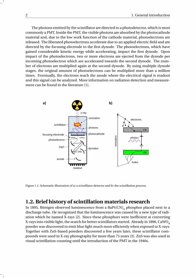
1.1. Radiation detectionIn order to protect ourselves from the harmful effects of ionizing radiation, it is essen-tial that we can accurately measure the incoming ionizing radiation. For the detectionof ionizing radiation a scintillator can be used. In short, a scintillator material convertsthe energy of the incoming radiation into multiple photons with lower energy, usuallyin the visible part of the spectrum. The emitted scintillation light, the amount of whichis a direct measure of the energy of the ionizing radiation, is then detected using a pho-todetector. There is a wide variety of scintillation materials used for radiation detection,e.g. single crystals, plastics, glasses, liquids and gases. This thesis focuses exclusively oninorganic scintillation crystals for the detection of high-energy photons (X- and γ-rays).
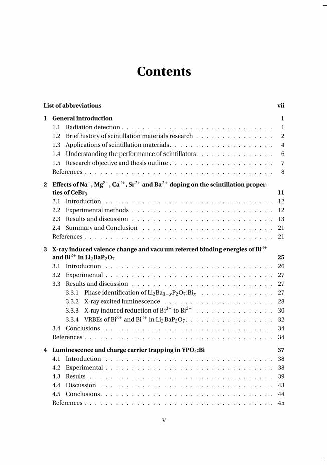
Fig. 1.1a schematically illustrates the detection of ionizing radiation using a scintil-lator crystal coupled to a photomultiplier tube (PMT). γ-rays emitted by a radioactivesource are absorbed by the scintillator material. As a result of photoelectric absorp-tion or Compton scattering of the γ-radiation by the scintillation material, an electron isknocked out of its orbit around the nucleus and gains the absorbed energy in the formof kinetic energy. This ionization process is shown in more detail in Fig. 1.1b. The high-energy electron travels through the scintillator and forms an ionization track as it slowsdown while losing kinetic energy. The now mobile electrons and holes of the ionizationtrack lose energy via thermalization until reaching the bottom of the conduction band(CB) and the top of the valence band (VB), respectively. The electrons and holes migrateto a luminescence recombination center, which is intentionally added to the scintillatorin the form of a dopant/activator ion to enhance the probability of photon emission. Aninorganic scintillation material is an insulator with typically a band gap of 4–12 eV. Theground state (GS) and excited state (ES) of the dopant ion are located inside the band gapof the host compound. This allows the electron and hole to recombine on the dopantion, releasing the energy in the form of a visible photon. The wavelength of the emittedphoton strongly depends on the dopant ion and its chemical environment provided bythe host lattice. Due to the high-energy of the incoming γ-ray (keV–GeV), the resultingscintillation pulse may contain several hundreds of thousands of visible photons.
1
2 1. General introduction
The photons emitted by the scintillator are directed to a photodetector, which is mostcommonly a PMT. Inside the PMT, the visible photons are absorbed by the photocathodematerial and, due to the low work function of the cathode material, photoelectrons arereleased. The liberated photoelectrons accelerate due to an applied electric field and aredirected by the focusing electrode to the first dynode. The photoelectrons, which havegained considerable kinetic energy while accelerating, impact the first dynode. Uponimpact of the photoelectrons, two or more electrons are ejected from the dynode perincoming photoelectron which are accelerated towards the second dynode. The num-ber of electrons are multiplied again at the second dynode. By using multiple dynodestages, the original amount of photoelectrons can be multiplied more than a milliontimes. Eventually, the electrons reach the anode where the electrical signal is readoutand this signal can be analyzed. More information on radiation detection and measure-ment can be found in the literature [1].
etc.
readout
PMT
photocathode focusing electrode
dynodes
anode
γ-ray
photons
photoelectron
holes
VB
CB
electrons
scintillator
photon
ioni
zatio
n ionization
a) b)
Figure 1.1: Schematic illustration of a) a scintillator detector and b) the scintillation process.
1.2. Brief history of scintillation materials researchIn 1895, Röntgen observed luminescence from a BaPt(CN)4 phosphor placed next to adischarge tube. He recognized that the luminescence was caused by a new type of radi-ation which he named X-rays [2]. Since these phosphors were inefficient at convertingX-rays into visible light, the search for better scintillators started. Already in 1896, CaWO4powder was discovered to emit blue light much more efficiently when exposed to X-rays.Together with ZnS-based powders discovered a few years later, these scintillator com-pounds were used in X-ray photography for more than 75 years [3]. ZnS was also used invisual scintillation counting until the introduction of the PMT in the 1940s.
1.2. Brief history of scintillation materials research 3
In the late 1940s, Hofstadter discovered the single-crystal scintillator NaI:Tl whichis still the most commonly used scintillator for γ-ray spectroscopy [4]. This was alsothe start of a new boost in scintillation materials research, resulting in the discovery ofmany new scintillators, e.g. CdWO4, CsI:Tl and glass scintillators activated with cerium.Steadily over the next decades, new scintillator materials were discovered of which theextraordinary fast BaF2 and very dense Bi4Ge3O12 are most notable. In the 1990s, drivenby the need for denser scintillators for high-energy physics and higher light yield scintil-lators for medical imaging, a new uplift in scintillation material research occurred. Thisled to the development of the high density and very fast PbWO4 scintillation materialfor the CMS detector in the LHC at CERN. For medical PET scanners, Lu2SiO5:Ce3+ wasfound to excel Bi4Ge3O12, the most commonly used material at that time, in terms ofhigher light yield and faster decay time.
Since 2000, scintillation materials research focused mainly on Ce3+ and Eu2+ acti-vated halide scintillators. LaBr3:Ce3+ and SrI2:Eu2+ are two examples of materials thatwere discovered with excellent scintillation properties, such as a record high light yieldof up to 120000 photons emitted per MeV of absorbed ionizing radiation energy andexcellent energy resolution of down to 3.0% at 662 keV γ-excitation. Later, the energyresolution of LaBr3:Ce3+ crystals was even further improved to a value of only 2.0% byco-doping the crystal with a small amount of Sr2+ [5].
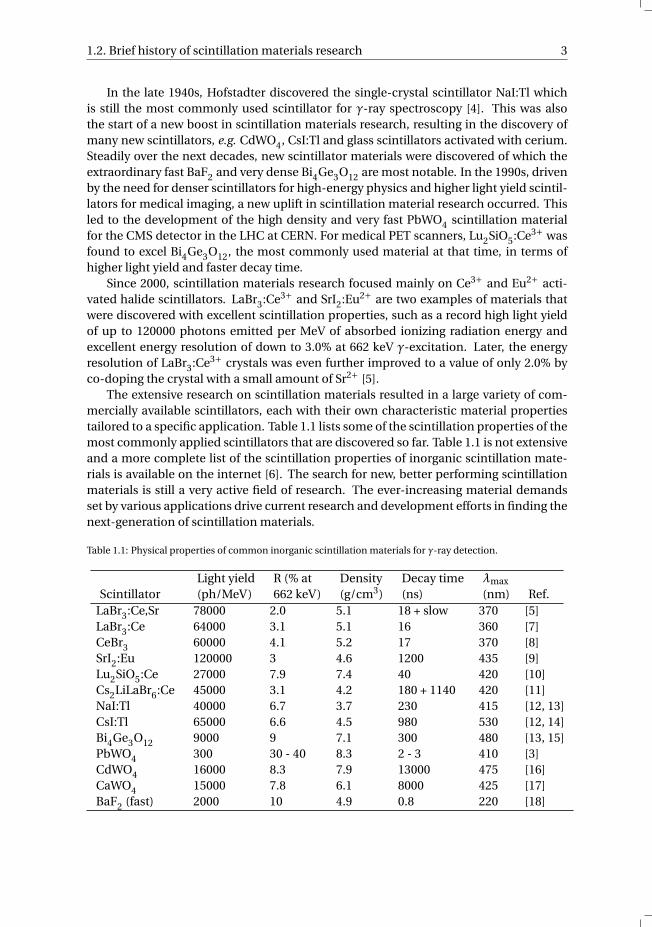
The extensive research on scintillation materials resulted in a large variety of com-mercially available scintillators, each with their own characteristic material propertiestailored to a specific application. Table 1.1 lists some of the scintillation properties of themost commonly applied scintillators that are discovered so far. Table 1.1 is not extensiveand a more complete list of the scintillation properties of inorganic scintillation mate-rials is available on the internet [6]. The search for new, better performing scintillationmaterials is still a very active field of research. The ever-increasing material demandsset by various applications drive current research and development efforts in finding thenext-generation of scintillation materials.
Table 1.1: Physical properties of common inorganic scintillation materials for γ-ray detection.
Light yield R (% at Density Decay time λmax
Scintillator (ph/MeV) 662 keV) (g/cm3) (ns) (nm) Ref.LaBr3:Ce,Sr 78000 2.0 5.1 18 + slow 370 [5]LaBr3:Ce 64000 3.1 5.1 16 360 [7]CeBr3 60000 4.1 5.2 17 370 [8]SrI2:Eu 120000 3 4.6 1200 435 [9]Lu2SiO5:Ce 27000 7.9 7.4 40 420 [10]Cs2LiLaBr6:Ce 45000 3.1 4.2 180 + 1140 420 [11]NaI:Tl 40000 6.7 3.7 230 415 [12, 13]CsI:Tl 65000 6.6 4.5 980 530 [12, 14]Bi4Ge3O12 9000 9 7.1 300 480 [13, 15]PbWO4 300 30 - 40 8.3 2 - 3 410 [3]CdWO4 16000 8.3 7.9 13000 475 [16]CaWO4 15000 7.8 6.1 8000 425 [17]BaF2 (fast) 2000 10 4.9 0.8 220 [18]
4 1. General introduction
1.3. Applications of scintillation materialsEach application in which scintillators are used has its own set of specific material re-quirements. Some of the most important requirements for scintillation materials usedfor γ-ray detection are (not necessarily in this order):
1. High light yield2. Excellent energy resolution3. Proportional scintillation response4. Low cost5. High density6. High effective atomic number7. Fast decay time8. Short rise time9. No self-absorption
10. No afterglow11. Emission wavelength matches photodetector sensitivity12. Refractive index matches photodetector window material13. No internal radioactivity14. High temperature stability15. Excellent radiation hardness16. High mechanical strength17. Able to grow large crystals18. Non hygroscopic
The following paragraphs provide a brief overview of the material requirements for eachapplication.
Medical diagnostics Scintillation materials are used in several medical diagnostics andimaging techniques such as X-ray computed tomography, single-photon emission com-puted tomography (SPECT) and positron emission tomography (PET). In order to exposea patient to the lowest amount of radiation as possible, a high detection efficiency is cru-cial. This requires scintillation materials with a high light yield, a high density and higheffective atomic number. A short rise time and fast scintillation decay time are essen-tial for time-of-flight PET measurements and for short acquisition times. For X-ray to-mography, Gd2O2S:Pr,Ce,F and (Y,Gd)2O3:Eu,Pr ceramic scintillators are the most widelyused. NaI:Tl and CsI:Tl are currently favored as scintillator in SPECT scanners. Due toits high density and reasonably fast decay time, Bi4Ge3O12 used to be the material ofchoice in PET scanners. However, Lu2SiO5:Ce offers an even faster decay time and muchhigher light yield and is therefore replacing Bi4Ge3O12 in these scanners. Drawbacks ofLu2SiO5:Ce are the difficulties in growing large, good quality crystals and the high priceof lutetium. LaBr3:Ce has been considered to replace the current scintillators for SPECTand PET, however, high production costs and too low density are limiting its commer-cialization for these applications. A more detailed discussion of scintillator materials formedical diagnostics can be found in Ref. [19].
1.3. Applications of scintillation materials 5
High-energy physics High-energy physics experiments, such as the particle accelera-tors at CERN, require very high density scintillators in order to efficiently stop and detectthe extremely high-energy (GeV - TeV) radiation. It also requires the scintillation mate-rial to have an excellent radiation hardness. For the L3 detector in the Large Electron-Positron Collider at CERN, nearly 12000 Bi4Ge3O12 crystals of 24 cm were used [20].While for the CMS detector in the LHC, more than 75000 PbWO4 crystals of 23 cm wereused [21]. Both scintillation materials have high densities and have a high effectiveatomic number which makes them ideal candidates for use in high-energy physics ex-periments. The large quantities of material used in these detectors require that the scin-tillator can be grown in large volumes at low cost. On the other hand, the amount ofenergy deposited in the scintillation material is so large that a relatively low light yieldof for example only 300 ph/MeV for PbWO4 is already acceptable. Furthermore, a fastscintillation decay time is required that is at least faster than the collision rate in the par-ticle accelerator. More information on scintillation materials and their requirements forhigh-energy physics can be found in Refs. [22] and [23].
Astrophysics and space exploration Scintillation materials are used in astrophysicsexperiments, for example to detect the characteristic X-rays emitted by newly formedstars or to study the radiation coming from supernova and other astrophysical events.γ-ray spectrometers containing scintillation materials are also put on-board spacecraftfor planetary remote sensing. This provides valuable information regarding the planet’selemental surface composition. To accurately monitor and differentiate between thevarious emitted energies coming from the surface, a high energy resolution is necessary.Furthermore, the amount of radiation reaching the spacecraft is very low, which requiresa high sensitivity. Essential for these low count-rate applications is to have an as low aspossible background noise, which requires the scintillator to have sufficiently low in-ternal radioactivity. Previously, only high-purity germanium detectors met the require-ments to be used as γ-ray spectrometers for space applications. Since 2000, LaBr3:Cescintillators provide excellent energy resolution, high sensitivity and room temperatureoperability that can compete with the semiconductor detectors [24]. In the last decade,LaBr3:Ce scintillator detectors were developed for the European Space Agency’s Bepi-Colombo mission to Mercury [25]. Unfortunately, LaBr3:Ce contains a small amount ofthe naturally occurring radioactive 138La isotope, which spoils its capability in low noiseapplications. Despite a slightly worse energy resolution, CeBr3 emerged as a promisingalternative to LaBr3:Ce as it has an almost 30× lower internal activity.
Security and environmental monitoring Machines for luggage screening at airportsand container scanning at naval ports contain scintillation materials. Most of the mod-ern scanners operate in the same way as X-ray computed tomography scanners for med-ical diagnostics to image the contents inside a bag or container. A high light yield andfast decay time are the most important requirements for fast and accurate image acquisi-tion. Also the protection from terrorism and monitoring of radiation from environmen-tal disasters (like Chernobyl and Fukushima) requires accurate detection of dangerousneutron and/or gamma-emitting materials. In both cases, the amount of radiation is lowwhich requires high light yield scintillators for a high sensitivity. A high energy resolu-
6 1. General introduction
tion and good neutron/gamma discrimination are required for accurate isotope identi-fication. Furthermore, low cost scintillation materials are needed for mass production ofthese radiation detectors. Scintillation materials that meet these requirements and arecurrently under development are Cs2LiYCl6:Ce, Cs2LiLaBr6:Ce and SrI2:Eu.
Geophysical and well logging Gamma-ray detectors are used to remotely measure thenatural radioactivity of the different soil layers of a drilled well or borehole. When thescintillator detector is lowered into a drilled well, it records the geophysical data as func-tion of the well depth in a gamma-ray log. These gamma-ray logs are used in the searchfor oil and mineral sources but also to gather information on the age and formation ofrock and soil layers. With temperatures over 200 ◦C and shock and vibrations encoun-tered during operation, the scintillation materials used for well logging should have ahigh temperature stability and should be mechanically rugged. Furthermore, these scin-tillation materials should also have a high density, high effective atomic number, fast de-cay and should be non-hygroscopic to avoid the need of special packaging [26]. So far noscintillation material exists which meets all of these requirements. For most well loggingapplications NaI:Tl is used, however, Bi4Ge3O12 and BaF2 are in some cases favored.
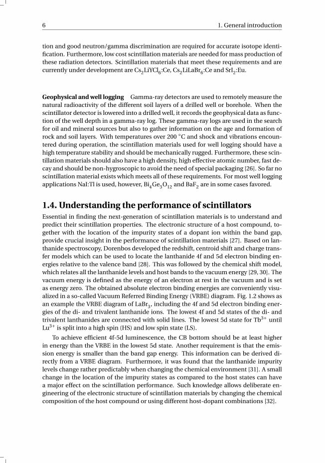
1.4. Understanding the performance of scintillatorsEssential in finding the next-generation of scintillation materials is to understand andpredict their scintillation properties. The electronic structure of a host compound, to-gether with the location of the impurity states of a dopant ion within the band gap,provide crucial insight in the performance of scintillation materials [27]. Based on lan-thanide spectroscopy, Dorenbos developed the redshift, centroid shift and charge trans-fer models which can be used to locate the lanthanide 4f and 5d electron binding en-ergies relative to the valence band [28]. This was followed by the chemical shift model,which relates all the lanthanide levels and host bands to the vacuum energy [29, 30]. Thevacuum energy is defined as the energy of an electron at rest in the vacuum and is setas energy zero. The obtained absolute electron binding energies are conveniently visu-alized in a so-called Vacuum Referred Binding Energy (VRBE) diagram. Fig. 1.2 shows asan example the VRBE diagram of LaBr3, including the 4f and 5d electron binding ener-gies of the di- and trivalent lanthanide ions. The lowest 4f and 5d states of the di- andtrivalent lanthanides are connected with solid lines. The lowest 5d state for Tb3+ untilLu3+ is split into a high spin (HS) and low spin state (LS).
To achieve efficient 4f-5d luminescence, the CB bottom should be at least higherin energy than the VRBE in the lowest 5d state. Another requirement is that the emis-sion energy is smaller than the band gap energy. This information can be derived di-rectly from a VRBE diagram. Furthermore, it was found that the lanthanide impuritylevels change rather predictably when changing the chemical environment [31]. A smallchange in the location of the impurity states as compared to the host states can havea major effect on the scintillation performance. Such knowledge allows deliberate en-gineering of the electronic structure of scintillation materials by changing the chemicalcomposition of the host compound or using different host-dopant combinations [32].
1.5. Research objective and thesis outline 7
- 1 2
- 1 0
- 8
- 6
- 4
- 2
0
2
Y b
VRBE
(eV)
E C B E X E V B L o w e s t 4 f L n 2 +
L o w e s t 5 d L n 2 +
L o w e s t 4 f L n 3 +
L o w e s t 5 d L n 3 + H S L o w e s t 5 d L n 3 + L S A l l 4 f L n 2 +
A l l 4 f L n 3 +
G dL a C e P r N d P m S m E u T b D y H o E r T m L u
L a B r 3
Figure 1.2: The vacuum referred binding energies of the divalent (red) and trivalent (blue) lanthanide 4f and5d electrons in LaBr3. EX is the binding energy in the host exciton.
1.5. Research objective and thesis outlineWith all the stable elements of the periodic table at our disposal to synthesize host com-pounds, there are an uncountable number of scintillator host lattices available. Com-bined with a suitable dopant ion, which is not limited to the lanthanides but also com-prise the transition metal and post-transition metal ions, this provides an almost infiniteresearch field on scintillation materials development. The general aim of the researchdescribed in this thesis is to explore the next-generation of scintillation materials. Sup-ported by the VRBE diagrams described in section 1.4, new avenues of scintillation ma-terials research and development are investigated.
Currently, most research is focused on halide crystals with lanthanide dopants andCe3+ in particular. However, extensive research efforts on these type of materials havealready been performed over the last decades. These Ce3+-doped halide materials havealmost reached their theoretical maximum light yield, which allows only little room forfinding new, better performing Ce3+-doped halides. An alternative to finding new ma-terials is to improve the scintillation properties of existing scintillation materials. Chap-ter 2 discusses such an approach by means of aliovalent doping of CeBr3. The effectsof Na+, Mg2+, Ca2+, Sr2+ and Ba2+ doping on the scintillation properties of CeBr3 areinvestigated.
Another direction in the field of scintillation materials is the search for longer wave-length (red-to-infrared) emitting scintillators. The red-to-infrared emission wavelengthsmatch with the sensitivity of modern photodiodes. Unlike PMTs, scintillator photodiodedetectors are small, operate at low voltage, are rugged and are insensitive to magneticfields, which makes them ideally suited as radiation detectors on-board spacecraft and
8 References
in PET scanners combined MRI. Furthermore, by engineering red-emitting scintillationmaterials with a smaller bandgap it is possible to go to even higher light yields. Chap-ters 3 and 4 are focused on Bi2+, a relatively new dopant ion in the field of scintillationmaterials with red-to-infrared emission wavelengths. Chapter 3 discusses the X-ray in-duced valence change of Bi3+ to Bi2+ and the luminescence and scintillation propertiesof bismuth doped Li2BaP2O7. Chapter 4 deals with the luminescence and charge carriertrapping in YPO4:Bi.
New scintillation materials with higher densities and higher effective atomic num-ber are of particular interest for high-energy physics experiments. However, with halidecrystals it is not possible to achieve densities higher than 6 g/cm3. With scintillationmaterials based on oxides it is possible to go to densities beyond 8 g/cm3. Even moreattractive would be oxides containing high effective atomic number elements such asTl, Pb or Bi. In order to evaluate if Ce3+ can luminescence efficiently in these type ofhost compounds, knowledge on the impurity levels of these post-transition metal ionsrelative to the host conduction and valence bands is required. This is the topic of chap-ters 5, 6 and 7. Chapter 5 deals with the electron binding energies in the impurity levelsof Bi3+ and how these change in relation to the chemical environment. Based on theelectron binding energies in the impurity levels in Bi3+ of chapter 5, together with elec-tron binding energies in the impurity levels in Bi2+, a concentration quenching modelof the Bi3+ luminescence via election transfer between bismuth pairs is introduced inchapter 6. Chapter 7 reviews the electron binding energies in the impurity levels of Pb2+and Tl+ in different inorganic compounds and compares the obtained results with thoseof Bi3+ from chapter 5.
References[1] G. F. Knoll, Radiation detection and measurement (John Wiley and Sons, New York,
2000).
[2] W. C. Röntgen, Ueber eine neue Art von Strahlen, Annalen der Physik 300, 1 (1898).
[3] M. Nikl, Scintillation detection for X-rays, Meas. Sci. Technol. 17, R37 (2006).
[4] R. Hofstadter, The detection of gamma-rays with thallium-activated sodium iodidecrystals, Phys. Rev. B 75, 796 (1949).
[5] M. S. Alekhin, J. T. M. de Haas, I. V. Khodyuk, K. W. Krämer, P. R. Menge, V. Ouspenski,and P. Dorenbos, Improvement of γ-ray energy resolution of LaBr3:Ce3+ scintillationdetectors by Sr2+ and Ca2+ co-doping, Appl. Phys. Lett. 102, 161915 (2013).
[6] S. Derenzo, M. Boswell, M. Weber, and K. Brennan, http: // scintillator. lbl.gov , (May 2017).
[7] M. S. Alekhin, D. A. Biner, K. W. Krämer, and P. Dorenbos, Improvement ofLaBr3:5%Ce scintillation properties by Li+, Na+, Mg2+, Ca2+, Sr2+ and Ba2+ co-doping, J. Appl. Phys. 113, 224904 (2013).
References 9
[8] F. G. A. Quarati, P. Dorenbos, J. van der Biezen, A. Owens, M. Selle, L. Parthier,and P. Schotanus, Scintillation and detection characteristics of high-sensitivity CeBr3gamma-ray spectrometers, Nucl. Instrum. Methods Phys. Res. A 729, 596 (2013).
[9] E. V. D. van Loef, C. M. Wilson, N. J. Cherepy, G. Hull, S. A. Payne, W.-S. Choong,W. W. Moses, and K. S. Shah, Crystal growth and scintillation properties of strontiumiodide scintillators, IEEE Trans. Nucl. Sci. 56, 869 (2009).
[10] C. L. Melcher, J. S. Schweitzer, C. A. Peterson, R. A. Manente, and H. Suzuki, Crystalgrowth and scintillation properties of the rare earth orthosilicates, Inorganic Scintil-lators and Their Applications, Delft University Press (SCINT95) , 309 (1996).
[11] P. R. Menge, J. Lejay, and V. Ouspenski, Design and performance of a com-pact Cs2LiLiBr6(Ce) neutron/gamma detector using silicon photomultipliers, IEEENSS/MIC Conference Proceedings (2015).
[12] C. W. E. van Eijk, P. Dorenbos, E. V. D. van Loef, K. W. Krämer, and H. U. Güdel, En-ergy resolution of some new inorganic-scintillator gamma-ray detectors, Rad. Meas.33, 521 (2001).
[13] E. Sakai, Recent measurements on scintillator-photodetector systems, IEEE Trans.Nucl. Sci. NS-34, 418 (1987).
[14] B. C. Grabmaier, Crystal scintillators, IEEE Trans. Nucl. Sci. NS31, 372 (1984).
[15] G. Blasse, Scintillator materials, Chem. Mater. 6, 1465 (1994).
[16] W. Klamra, T. Szczesniak, M. Moszynski, J. Iwanowska, L. Swiderski, A. Syntfeld-Kazuch, V. N. Shlegel, Y. V. Vasiliev, and E. N. Galashov, Properties of CdWO4 andZnWO4 scintillators at liquid nitrogen temperature, JINST 7, P03011 (2012).
[17] Y. G. Zdesenko, F. T. Avignone, V. B. Brudanin, F. A. Danevich, S. S. Nagorny, I. . M.Solsky, and V. I. Tretyak, Scintillation properties and radioactive contamination ofCaWO4 crystal scintillators, Nucl. Instrum. Methods Phys. Res. A 538, 657 (2005).
[18] M. Laval, M. Moszynski, R. Allemand, E. Cormoreche, P. Guinet, R. Odru, andJ. Vacher, Barium fluoride - inorganic scintillator for subnanosecond timing, Nucl.Instrum. Methods Phys. Res. A 206, 169 (1983).
[19] C. W. E. van Eijk, Inorganic scintillators in medical imaging, Phys. Med. Biol. 47, R85(2002).
[20] R. Sumner, The L3 BGO electromagnetic calorimeter, Nucl. Instrum. Methods Phys.Res. A 265, 252 (1988).
[21] C. Biino, The CMS electromagnetic calorimeter: overview, lessons learned during Run1 and future projections, J. Phys.: Conf. Series 587, 012001 (2015).
[22] P. Lecoq, The high energy physics demand for a new generation of scintillators, J.Lumin. 60, 948 (1994).
10 References
[23] R. Mao, L. Zhang, and R. Y. Zhu, Optical and scintillation properties of inorganicscintillators in high energy physics, IEEE Trans. Nucl. Sci. 55, 2425 (2008).
[24] C. C. T. Hansson, A. Owens, B. Shortt, P. Dorenbos, F. Quarati, R. Williams, D. Hahn,T. Toepfer, L. Pathier, P. Schotanus, J. v.d. Biezen, K. N. O’Neill, C. Jackson, andL. Wall, Development of low noise scintillator crystals for planetary space missions,IEEE NSS/MIC Conference Proceedings NS14-241, 927 (2012).
[25] I. G. Mitrofanov, A. S. Kozyrev, A. Konovalov, M. L. Litvak, A. A. Malakhov, M. I.Mokrousov, A. B. Sanin, V. I. Tret’ykov, A. V. Vostrukin, Y. I. Bobrovniskij, T. M.Tomilina, L. Gurvits, and A. Owens, The Mercury Gamma and Neutron Spectrome-ter (MGNS) on board the planetary orbiter of the Bepicolombo mission, Planet. SpaceSci. 58, 116 (2010).
[26] C. L. Melcher, Scintillators for well logging applications, Nucl. Instrum. MethodsPhys. Res. B 40-41, 1214 (1989).
[27] P. Dorenbos, Determining binding energies of valence-band electrons in insulatorsand semiconductors via lanthanide spectroscopy, Phys. Rev. B 87, 035118 (2013).
[28] P. Dorenbos, A review on how lanthanide impurity levels change with chemistry andstructure of inorganic compounds, ECS J. Solid State Sci. Technol. 2, R3001 (2013).
[29] P. Dorenbos, Modeling the chemical shift of lanthanide 4f electron binding energies,Phys. Rev. B 85, 165107 (2012).
[30] P. Dorenbos, Ce3+ 5d-centroid shift and vacuum referred 4f-electron binding energiesof all lanthanide impurities in 150 different compounds, J. Lumin. 135, 93 (2013).
[31] P. Dorenbos, Electron binding energies and how it relates to activator luminescenceand bonding in compounds, J. Lumin. 169, 381 (2016).
[32] P. Dorenbos, Electronic structure engineering of lanthanide activated materials, J.Mater. Chem. 22, 22344 (2012).
2Effects of Na+, Mg2+, Ca2+, Sr2+ and Ba2+
doping on the scintillation properties ofCeBr3
The effects of Na+, Mg2+, Ca2+, Sr2+ and Ba2+ doping on the scintillation properties ofCeBr3 are evaluated in this chapter. Ca2+ and Sr2+ doped CeBr3 show different scintil-lation properties as compared to undoped CeBr3, i.e. an additional perturbed Ce3+ sitewith emission maxima red-shifted by 30 nm compared to unperturbed Ce3+ sites as evi-denced by X-ray excited emission and photoluminescence measurements. Also a nearlyconstant light yield at temperatures below 300 K, an increased decay time and the ap-pearance of multiple glow peaks in thermoluminescence measurements are observedfor Ca and Sr doped CeBr3. These effects on the scintillation properties of CeBr3 are ex-plained using a single trap model where Br vacancies, formed as charge compensationfor the aliovalent dopants, act as electron traps.
This chapter is based on the publication: R. H. P. Awater, K. W. Krämer and P. Doren-bos, “Effects of Na+, Mg2+, Ca2+, Sr2+ and Ba2+ doping on the scintillation properties ofCeBr3”, IEEE Transactions on Nuclear Science 62 (2015), 2343.
11
12 Effects of doping on the scintillation properties of CeBr3
2.1. IntroductionSince the invention of the photomultiplier tube and the discovery of NaI:Tl+ crystal scin-tillators in the 1940’s, many new scintillator materials have been discovered and inves-tigated for the detection of gamma radiation. However, even at present time NaI:Tl+ isstill the most commonly used scintillator worldwide. With the discovery of LaBr3:Ce in2001, a new material combining a high light yield of 70,000 photons per MeV of absorbedgamma ray energy, excellent energy resolution of 2.8% for 662 keV gamma ray detectionand a short scintillation pulse decay time of 15 ns was obtained [1].
A major drawback of LaBr3:Ce is that it contains 138La isotopes that causes an intrin-sic activity which spoils the capability of LaBr3:Ce in low count rate experiments [2]. Thedrastically reduced intrinsic activity due to the absence of naturally occurring isotopesmakes CeBr3 a more interesting scintillator for the detection of low intensity gamma raysources compared to LaBr3:Ce. Below 3 MeV, the detection sensitivity of CeBr3 is 5×higher than for LaBr3:Ce and up to 16× higher for detection of 40K [3, 4]. Because of theincreased detection sensitivity, CeBr3 offers superior performance for applications suchas planetary remote sensing, homeland security and radionuclide identification [5–7].Unfortunately CeBr3 shows a poorer energy resolution of 4% at 662 keV compared to 3%for LaBr3:5%Ce [3].
Because of the hexagonal crystal structure (space group P63/m) of CeBr3 and lan-thanide halides in general, the crystals have anisotropic thermal expansion and plas-ticity resulting in build-up of stresses in the material during growth [8]. Together withthe tendency to fracture along the prismatic slip planes, these materials are very brit-tle. Attempts were made to improve the crystal strength by aliovalent doping withoutnegatively influencing the scintillation properties. Interestingly, the use of alkaline earthmetals as dopant was shown to improve the energy resolution of LaBr3:Ce and CeBr3
considerably for small crystal samples. Sr2+ as a dopant improved the energy resolutionto a value of 2% in LaBr3:5%Ce [9], while Ca2+ as a dopant improved the energy resolu-tion of CeBr3 to 3.2% [10]. This improvement in energy resolution of the doped sampleswas ascribed to a more proportional response of the light yield compared to standardLaBr3:5%Ce or CeBr3. The exact origin of this improvement due to aliovalent doping re-mains controversial. A possible explanation by Åberg et al. is that the aliovalent dopantscreate Br vacancies acting as electron traps, which reduces Auger quenching of free car-riers and that is expected to improve the linearity of the light yield as function of theenergy of the incident radiation [11].
In a previous investigation, the energy resolution enhancement of Na+, Mg2+, Ca2+,Sr2+ and Ba2+ doped CeBr3 samples was evaluated and an energy resolution of down to3.0% for the Sr2+ doped sample was found [12]. In this chapter we report on the effectsof these same dopants on the scintillation properties of CeBr3.
2.2. Experimental methodsThe undoped and Na+, Mg2+, Ca2+, Sr2+ and Ba2+ doped CeBr3 crystals discussed inthis chapter were grown at the University of Bern by the vertical Bridgman technique insealed quartz ampoules and contained a nominal dopant concentration of 0.5%. It isexpected that at maximum only a few hundred ppm of dopant is actually incorporated
2.3. Results and discussion 13
in the crystal, since inductively coupled plasma analysis only showed 100-200 ppm ofSr2+ in Sr2+ co-doped LaBr3:Ce [13]. The crystals were grown as ingots of 8 mm in di-ameter of which 30 - 50 mm3 samples were cleaved. In a previous paper the effectiveenhancement of the energy resolution via aliovalent doping of the same CeBr3 sampleswas discussed [12]. For all temperature dependent measurements a Janis VPF-800 cryo-stat operated with a LakeShore 331 temperature controller were used. The cryostat wasbaked to remove all water from the system prior to sample mounting because of thehygroscopic nature of the CeBr3 crystals. The samples were mounted on the cold fin-ger of the cryostat in a nitrogen filled glovebox. The PMT’s were outside the cryostatand remained always at room temperature. X-ray excited emission and thermolumines-cence spectra were recorded using an X-ray tube with Cu anode operating at 60 kV and20 mA. The emission of the sample was focused via a quartz window and a lens on theentrance slit of an ARC VM504 monochromator (blazed at 300 nm, 1200 grooves/mm),dispersed, and recorded with a Hamamatsu R943–02 PMT. The spectra were correctedfor the monochromator transmission and the quantum efficiency of the PMT. For ther-moluminescence measurements the crystals were cooled down to 78 K and then irra-diated with X-rays for approximately 5 min leading to a steady state X-ray excited lu-minescence (SSL). The thermoluminescence emission was monitored at the respectiveemission maximum of the sample while heating with a constant rate of 6 K/min usinga Lakeshore 331 temperature controller. Photoluminescence excitation and emissionspectra were recorded using an OSRAM XBO450W/4 Suprasil Xenon lamp in combina-tion with a Horiba Gemini - 180 double grating monochromator. The emission light ofthe crystal was dispersed with a Princeton Instruments Acton SP 2300 monochromatorand detected by a Perkin Elmer Photon Counting Module MP1993. The excitation spec-tra were corrected for the lamp spectrum while no further correction was applied forthe emission spectra. Temperature dependent photoelectron yield measurements werederived from pulse height spectra which were recorded using a Hamamatsu R6231-100PMT at a voltage of -500 V, a 137Cs source (662 keV) and a 10 µs shaping time. The timecorrelated single photon counting method using a pulsed picosecond X-ray source wasused to record the scintillation time profiles. The X-ray tube with a S-20 type photocath-ode and tungsten anode was operated at a voltage of 40 kV (Emax = 40 keV). A HP 8116APulse/Function generator in combination with a Picoquant Sepia multi-channel laserdiode were used to trigger the X-ray pulses. An IDQ id100 single photon detection mod-ule was used as detector. In short, photoelectrons are liberated by the emitted photonsfrom the laser diode and are accelerated towards the anode, resulting in pulsed X-rayswhich are directed towards the sample. More detailed information on the pulsed X-raysetup can be found in [14].
2.3. Results and discussionFig. 2.1 shows the X-ray excited emission spectra of the studied CeBr3 crystals at 298 Kand 78 K. At room temperature, the undoped, Na+ and Mg2+ doped CeBr3 samples showtwo overlapping peaks at 367 nm and 388 nm. In the case of Ba2+ doped CeBr3 the twoemission peaks are hardly distinguishable. The emission bands of Sr2+ and Ca2+ dopedCeBr3 samples are slightly red-shifted and show a maximum emission at 381 nm with aside band at longer wavelengths. At 78 K the undoped, Na+, Mg2+ and Ba2+ doped CeBr3
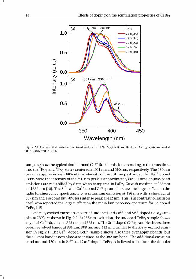
14 Effects of doping on the scintillation properties of CeBr3
0 . 0
0 . 5
1 . 0
3 5 0 4 0 0 4 5 00 . 0
0 . 5
1 . 0
3 6 7 n m 3 8 1 n m
Inten
sity (a
. u.)
W a v e l e n g t h ( n m )
C e B r 3 C e B r 3 : N a C e B r 3 : M g C e B r 3 : C a C e B r 3 : S r C e B r 3 : B a
3 6 1 n m 3 8 6 n m
4 1 2 n m
( a )
( b )
Figure 2.1: X-ray excited emission spectra of undoped and Na, Mg, Ca, Sr and Ba doped CeBr3 crystals recordedat (a) 298 K and (b) 78 K.
samples show the typical double-band Ce3+ 5d-4f emission according to the transitionsinto the 2F5/2 and 2F7/2 states centered at 361 nm and 390 nm, respectively. The 390 nmpeak has approximately 60% of the intensity of the 361 nm peak except for Ba2+ dopedCeBr3 were the intensity of the 390 nm peak is approximately 80%. These double-bandemissions are red-shifted by 5 nm when compared to LaBr3:Ce with maxima at 355 nmand 385 nm [13]. The Sr2+ and Ca2+ doped CeBr3 samples show the largest effect on theradio luminescence spectrum, i. e. a maximum emission at 386 nm with a shoulder at367 nm and a second but 70% less intense peak at 412 nm. This is in contrast to Harrisonet al. who reported the largest effect on the radio luminescence spectrum for Ba dopedCeBr3 [15].
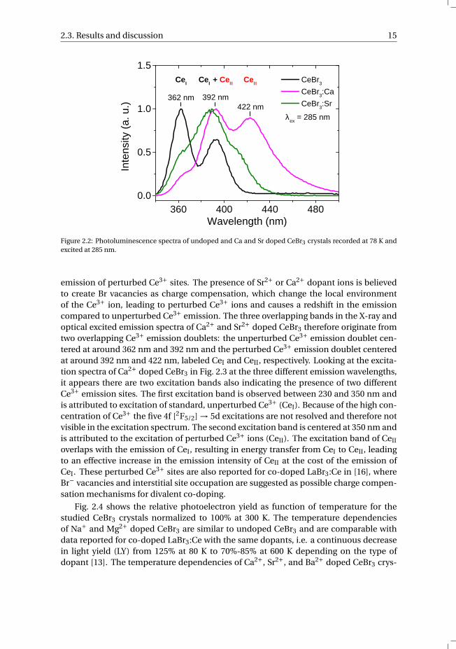
Optically excited emission spectra of undoped and Ca2+ and Sr2+ doped CeBr3 sam-ples at 78 K are shown in Fig. 2.2. At 285 nm excitation, the undoped CeBr3 sample showsa typical Ce3+ doublet at 362 nm and 392 nm. The Sr2+ doped CeBr3 sample shows threepoorly resolved bands at 366 nm, 388 nm and 412 nm, similar to the X-ray excited emis-sion in Fig. 2.1. The Ca2+ doped CeBr3 sample shows also three overlapping bands, butthe 422 nm band is now almost as intense as the 392 nm band. The additional emissionband around 420 nm in Sr2+ and Ca2+ doped CeBr3 is believed to be from the doublet
2.3. Results and discussion 15
3 6 0 4 0 0 4 4 0 4 8 00 . 0
0 . 5
1 . 0
1 . 5
Inten
sity (a
. u.)
W a v e l e n g t h ( n m )
C e B r 3 C e B r 3 : C a C e B r 3 : S r3 6 2 n m 3 9 2 n m
4 2 2 n mλ e x = 2 8 5 n m
C e I C e I + C e I I C e I I
Figure 2.2: Photoluminescence spectra of undoped and Ca and Sr doped CeBr3 crystals recorded at 78 K andexcited at 285 nm.
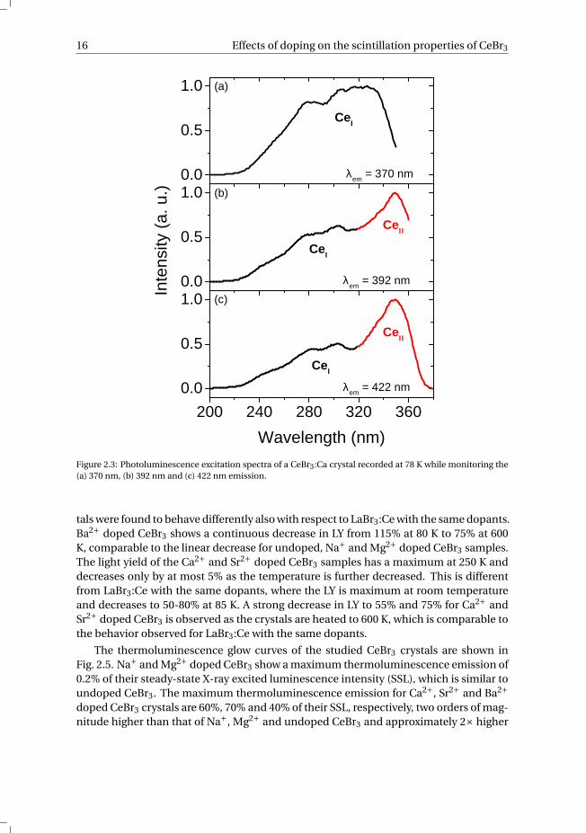
emission of perturbed Ce3+ sites. The presence of Sr2+ or Ca2+ dopant ions is believedto create Br vacancies as charge compensation, which change the local environmentof the Ce3+ ion, leading to perturbed Ce3+ ions and causes a redshift in the emissioncompared to unperturbed Ce3+ emission. The three overlapping bands in the X-ray andoptical excited emission spectra of Ca2+ and Sr2+ doped CeBr3 therefore originate fromtwo overlapping Ce3+ emission doublets: the unperturbed Ce3+ emission doublet cen-tered at around 362 nm and 392 nm and the perturbed Ce3+ emission doublet centeredat around 392 nm and 422 nm, labeled CeI and CeII, respectively. Looking at the excita-tion spectra of Ca2+ doped CeBr3 in Fig. 2.3 at the three different emission wavelengths,it appears there are two excitation bands also indicating the presence of two differentCe3+ emission sites. The first excitation band is observed between 230 and 350 nm andis attributed to excitation of standard, unperturbed Ce3+ (CeI). Because of the high con-centration of Ce3+ the five 4f [2F5/2] → 5d excitations are not resolved and therefore notvisible in the excitation spectrum. The second excitation band is centered at 350 nm andis attributed to the excitation of perturbed Ce3+ ions (CeII). The excitation band of CeII
overlaps with the emission of CeI, resulting in energy transfer from CeI to CeII, leadingto an effective increase in the emission intensity of CeII at the cost of the emission ofCeI. These perturbed Ce3+ sites are also reported for co-doped LaBr3:Ce in [16], whereBr− vacancies and interstitial site occupation are suggested as possible charge compen-sation mechanisms for divalent co-doping.
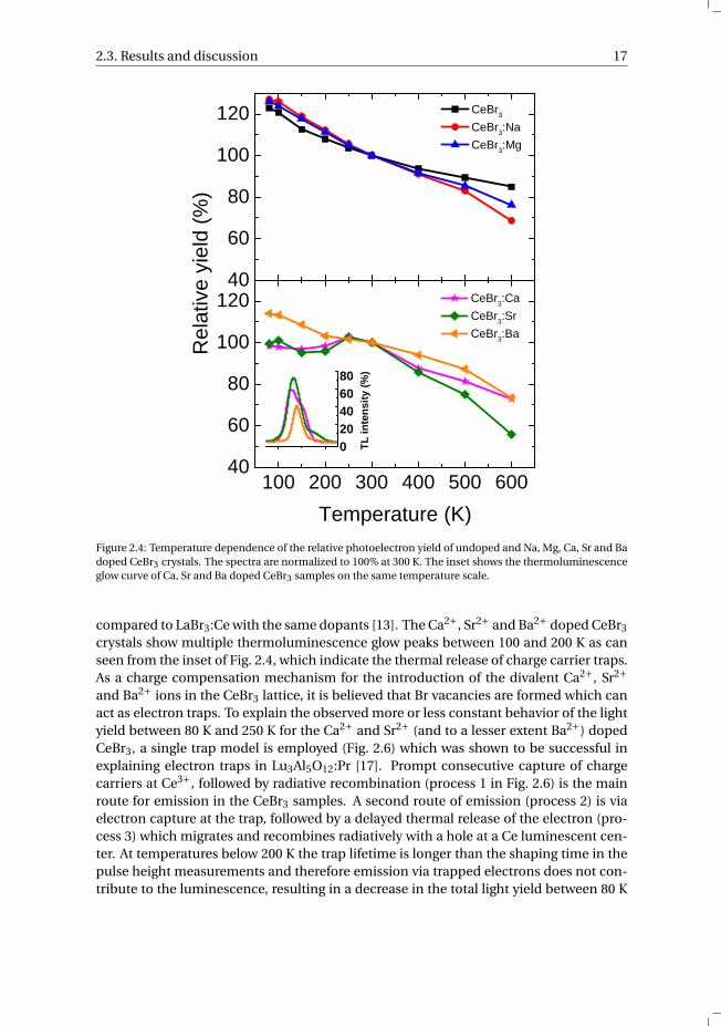
Fig. 2.4 shows the relative photoelectron yield as function of temperature for thestudied CeBr3 crystals normalized to 100% at 300 K. The temperature dependenciesof Na+ and Mg2+ doped CeBr3 are similar to undoped CeBr3 and are comparable withdata reported for co-doped LaBr3:Ce with the same dopants, i.e. a continuous decreasein light yield (LY) from 125% at 80 K to 70%-85% at 600 K depending on the type ofdopant [13]. The temperature dependencies of Ca2+, Sr2+, and Ba2+ doped CeBr3 crys-
16 Effects of doping on the scintillation properties of CeBr3
0 . 0
0 . 5
1 . 0
0 . 0
0 . 5
1 . 0
2 0 0 2 4 0 2 8 0 3 2 0 3 6 00 . 0
0 . 5
1 . 0
C e I
λ e m = 3 7 0 n m
C e I I
C e I I
C e I
C e I
Inten
sity (a
. u.)
λ e m = 3 9 2 n m( c )
( b )
( a )
W a v e l e n g t h ( n m )
λ e m = 4 2 2 n m
Figure 2.3: Photoluminescence excitation spectra of a CeBr3:Ca crystal recorded at 78 K while monitoring the(a) 370 nm, (b) 392 nm and (c) 422 nm emission.
tals were found to behave differently also with respect to LaBr3:Ce with the same dopants.Ba2+ doped CeBr3 shows a continuous decrease in LY from 115% at 80 K to 75% at 600K, comparable to the linear decrease for undoped, Na+ and Mg2+ doped CeBr3 samples.The light yield of the Ca2+ and Sr2+ doped CeBr3 samples has a maximum at 250 K anddecreases only by at most 5% as the temperature is further decreased. This is differentfrom LaBr3:Ce with the same dopants, where the LY is maximum at room temperatureand decreases to 50-80% at 85 K. A strong decrease in LY to 55% and 75% for Ca2+ andSr2+ doped CeBr3 is observed as the crystals are heated to 600 K, which is comparable tothe behavior observed for LaBr3:Ce with the same dopants.
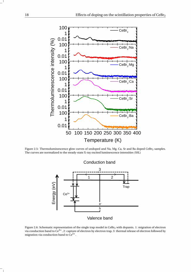
The thermoluminescence glow curves of the studied CeBr3 crystals are shown inFig. 2.5. Na+ and Mg2+ doped CeBr3 show a maximum thermoluminescence emission of0.2% of their steady-state X-ray excited luminescence intensity (SSL), which is similar toundoped CeBr3. The maximum thermoluminescence emission for Ca2+, Sr2+ and Ba2+doped CeBr3 crystals are 60%, 70% and 40% of their SSL, respectively, two orders of mag-nitude higher than that of Na+, Mg2+ and undoped CeBr3 and approximately 2× higher
2.3. Results and discussion 17
4 06 08 0
1 0 01 2 0
1 0 0 2 0 0 3 0 0 4 0 0 5 0 0 6 0 04 06 08 0
1 0 01 2 0
02 04 06 08 0
C e B r 3 C e B r 3 : N a C e B r 3 : M g
Relat
ive yie
ld (%
)
T e m p e r a t u r e ( K )
C e B r 3 : C a C e B r 3 : S r C e B r 3 : B a
TL in
tensit
y (%)
Figure 2.4: Temperature dependence of the relative photoelectron yield of undoped and Na, Mg, Ca, Sr and Badoped CeBr3 crystals. The spectra are normalized to 100% at 300 K. The inset shows the thermoluminescenceglow curve of Ca, Sr and Ba doped CeBr3 samples on the same temperature scale.
compared to LaBr3:Ce with the same dopants [13]. The Ca2+, Sr2+ and Ba2+ doped CeBr3
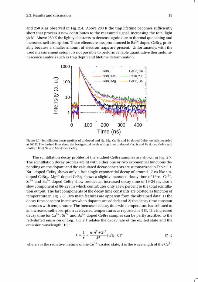
crystals show multiple thermoluminescence glow peaks between 100 and 200 K as canseen from the inset of Fig. 2.4, which indicate the thermal release of charge carrier traps.As a charge compensation mechanism for the introduction of the divalent Ca2+, Sr2+and Ba2+ ions in the CeBr3 lattice, it is believed that Br vacancies are formed which canact as electron traps. To explain the observed more or less constant behavior of the lightyield between 80 K and 250 K for the Ca2+ and Sr2+ (and to a lesser extent Ba2+) dopedCeBr3, a single trap model is employed (Fig. 2.6) which was shown to be successful inexplaining electron traps in Lu3Al5O12:Pr [17]. Prompt consecutive capture of chargecarriers at Ce3+, followed by radiative recombination (process 1 in Fig. 2.6) is the mainroute for emission in the CeBr3 samples. A second route of emission (process 2) is viaelectron capture at the trap, followed by a delayed thermal release of the electron (pro-cess 3) which migrates and recombines radiatively with a hole at a Ce luminescent cen-ter. At temperatures below 200 K the trap lifetime is longer than the shaping time in thepulse height measurements and therefore emission via trapped electrons does not con-tribute to the luminescence, resulting in a decrease in the total light yield between 80 K
18 Effects of doping on the scintillation properties of CeBr3
0 . 0 11
1 0 0
0 . 0 11
1 0 0
0 . 0 11
1 0 0
0 . 0 11
1 0 0
0 . 0 11
1 0 0
5 0 1 0 0 1 5 0 2 0 0 2 5 0 3 0 0 3 5 0 4 0 00 . 0 1
11 0 0
C e B r 3
C e B r 3 : N a
C e B r 3 : M g
Therm
olumi
nesce
nce i
ntens
ity (%
)
C e B r 3 : C a
C e B r 3 : S r
T e m p e r a t u r e ( K )
C e B r 3 : B a
Figure 2.5: Thermoluminescence glow curves of undoped and Na, Mg, Ca, Sr and Ba doped CeBr3 samples.The curves are normalized to the steady-state X-ray excited luminescence intensities (SSL)
Conduction band
Valence band
3
1
e- h
2
Ene
rgy
(eV
)
Ce3+
Trap
Figure 2.6: Schematic representation of the single trap model in CeBr3 with dopants. 1: migration of electronvia conduction band to Ce3+, 2: capture of electron by electron trap, 3: thermal release of electron followed bymigration via conduction band to Ce3+.
2.3. Results and discussion 19
and 250 K as observed in Fig. 2.4. Above 200 K the trap lifetime becomes sufficientlyshort that process 3 now contributes to the measured signal, increasing the total lightyield. Above 250 K the light yield starts to decrease again due to thermal quenching andincreased self absorption. These effects are less pronounced in Ba2+ doped CeBr3, prob-ably because a smaller amount of electron traps are present. Unfortunately, with theused measurement setup it is not possible to perform reliable quantitative thermolumi-nescence analysis such as trap depth and lifetime determination.
0 1 0 0 2 0 0 3 0 0 4 0 0
1
1 0
1 0 0
1 0 0 0
Int
ensity
(a. u
.)
T i m e ( n s )
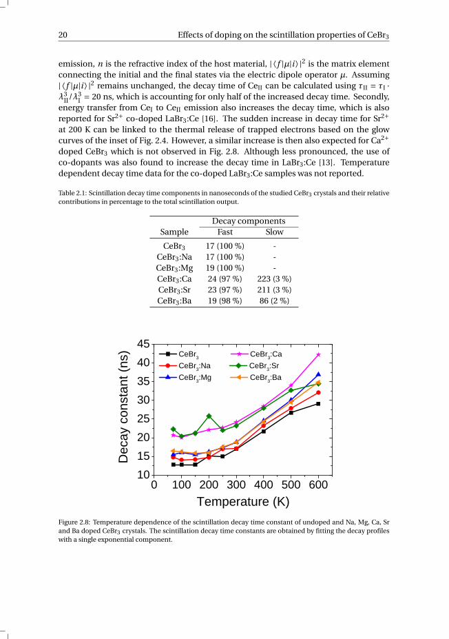
C e B r 3 C e B r 3 : C a C e B r 3 : N a C e B r 3 : S r C e B r 3 : M g C e B r 3 : B a
Figure 2.7: Scintillation decay profiles of undoped and Na, Mg, Ca, Sr and Ba doped CeBr3 crystals recordedat 300 K. The dashed lines show the background levels of (top line) undoped, Ca, Sr and Ba doped CeBr3 and(bottom line) Na and Mg doped CeBr3.
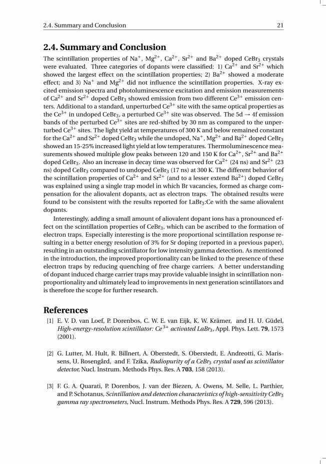
The scintillation decay profiles of the studied CeBr3 samples are shown in Fig. 2.7.The scintillation decay profiles are fit with either one or two exponential functions de-pending on the dopant and the calculated decay constants are summarized in Table 2.1.Na+ doped CeBr3 shows only a fast single exponential decay of around 17 ns like un-doped CeBr3. Mg2+ doped CeBr3 shows a slightly increased decay time of 19ns. Ca2+,Sr2+ and Ba2+ doped CeBr3 show besides an increased decay time of 19-24 ns, also aslow component of 86-223 ns which contributes only a few percent to the total scintilla-tion output. The fast components of the decay time constants are plotted as function oftemperature in Fig. 2.8. Two main features are apparent from the obtained data: 1) thedecay time constant increases when dopants are added; and 2) the decay time constantincreases with temperature. The increase in decay time with temperature is attributed toan increased self-absorption at elevated temperatures as reported in [18]. The increaseddecay time for Ca2+, Sr2+ and Ba2+ doped CeBr3 samples can be partly ascribed to thered-shifted emission of CeII. Eq. 2.1 relates the decay rate of the excited state and theemission wavelength [19]:
Γ= 1
τ∼ n(n2 +2)2
λ3 | ⟨ f |µ|i ⟩ |2 (2.1)
where τ is the radiative lifetime of the Ce3+ excited state, λ is the wavelength of the Ce3+
20 Effects of doping on the scintillation properties of CeBr3
emission, n is the refractive index of the host material, | ⟨ f |µ|i ⟩ |2 is the matrix elementconnecting the initial and the final states via the electric dipole operator µ. Assuming| ⟨ f |µ|i ⟩ |2 remains unchanged, the decay time of CeII can be calculated using τII = τI ·λ3
II/λ3I = 20 ns, which is accounting for only half of the increased decay time. Secondly,
energy transfer from CeI to CeII emission also increases the decay time, which is alsoreported for Sr2+ co-doped LaBr3:Ce [16]. The sudden increase in decay time for Sr2+at 200 K can be linked to the thermal release of trapped electrons based on the glowcurves of the inset of Fig. 2.4. However, a similar increase is then also expected for Ca2+doped CeBr3 which is not observed in Fig. 2.8. Although less pronounced, the use ofco-dopants was also found to increase the decay time in LaBr3:Ce [13]. Temperaturedependent decay time data for the co-doped LaBr3:Ce samples was not reported.
Table 2.1: Scintillation decay time components in nanoseconds of the studied CeBr3 crystals and their relativecontributions in percentage to the total scintillation output.
Decay componentsSample Fast Slow
CeBr3 17 (100 %) -CeBr3:Na 17 (100 %) -CeBr3:Mg 19 (100 %) -CeBr3:Ca 24 (97 %) 223 (3 %)CeBr3:Sr 23 (97 %) 211 (3 %)CeBr3:Ba 19 (98 %) 86 (2 %)
0 1 0 0 2 0 0 3 0 0 4 0 0 5 0 0 6 0 01 01 52 02 53 03 54 04 5
Deca
y con
stant
(ns)
T e m p e r a t u r e ( K )
C e B r 3 C e B r 3 : C a C e B r 3 : N a C e B r 3 : S r C e B r 3 : M g C e B r 3 : B a
Figure 2.8: Temperature dependence of the scintillation decay time constant of undoped and Na, Mg, Ca, Srand Ba doped CeBr3 crystals. The scintillation decay time constants are obtained by fitting the decay profileswith a single exponential component.
2.4. Summary and Conclusion 21
2.4. Summary and ConclusionThe scintillation properties of Na+, Mg2+, Ca2+, Sr2+ and Ba2+ doped CeBr3 crystalswere evaluated. Three categories of dopants were classified: 1) Ca2+ and Sr2+ whichshowed the largest effect on the scintillation properties; 2) Ba2+ showed a moderateeffect; and 3) Na+ and Mg2+ did not influence the scintillation properties. X-ray ex-cited emission spectra and photoluminescence excitation and emission measurementsof Ca2+ and Sr2+ doped CeBr3 showed emission from two different Ce3+ emission cen-ters. Additional to a standard, unperturbed Ce3+ site with the same optical properties asthe Ce3+ in undoped CeBr3, a perturbed Ce3+ site was observed. The 5d → 4f emissionbands of the perturbed Ce3+ sites are red-shifted by 30 nm as compared to the unper-turbed Ce3+ sites. The light yield at temperatures of 300 K and below remained constantfor the Ca2+ and Sr2+ doped CeBr3 while the undoped, Na+, Mg2+ and Ba2+ doped CeBr3
showed an 15-25% increased light yield at low temperatures. Thermoluminescence mea-surements showed multiple glow peaks between 120 and 150 K for Ca2+, Sr2+ and Ba2+doped CeBr3. Also an increase in decay time was observed for Ca2+ (24 ns) and Sr2+ (23ns) doped CeBr3 compared to undoped CeBr3 (17 ns) at 300 K. The different behavior ofthe scintillation properties of Ca2+ and Sr2+ (and to a lesser extend Ba2+) doped CeBr3
was explained using a single trap model in which Br vacancies, formed as charge com-pensation for the aliovalent dopants, act as electron traps. The obtained results werefound to be consistent with the results reported for LaBr3:Ce with the same aliovalentdopants.
Interestingly, adding a small amount of aliovalent dopant ions has a pronounced ef-fect on the scintillation properties of CeBr3, which can be ascribed to the formation ofelectron traps. Especially interesting is the more proportional scintillation response re-sulting in a better energy resolution of 3% for Sr doping (reported in a previous paper),resulting in an outstanding scintillator for low intensity gamma detection. As mentionedin the introduction, the improved proportionality can be linked to the presence of theseelectron traps by reducing quenching of free charge carriers. A better understandingof dopant induced charge carrier traps may provide valuable insight in scintillation non-proportionality and ultimately lead to improvements in next generation scintillators andis therefore the scope for further research.
References[1] E. V. D. van Loef, P. Dorenbos, C. W. E. van Eijk, K. W. Krämer, and H. U. Güdel,
High-energy-resolution scintillator: Ce 3+ activated LaBr3, Appl. Phys. Lett. 79, 1573(2001).
[2] G. Lutter, M. Hult, R. Billnert, A. Oberstedt, S. Oberstedt, E. Andreotti, G. Maris-sens, U. Rosengård, and F. Tzika, Radiopurity of a CeBr3 crystal used as scintillatordetector, Nucl. Instrum. Methods Phys. Res. A 703, 158 (2013).
[3] F. G. A. Quarati, P. Dorenbos, J. van der Biezen, A. Owens, M. Selle, L. Parthier,and P. Schotanus, Scintillation and detection characteristics of high-sensitivity CeBr3
gamma ray spectrometers, Nucl. Instrum. Methods Phys. Res. A 729, 596 (2013).
22 References
[4] A. F. Iyudin, V. V. Bogomolov, S. I. Svertilov, I. V. Yashin, N. V. Klassen, S. Z. Shmurak,and A. D. Orlov, Peculiarities of intrinsic background in LaBr3:Ce and CeBr3 scintil-lating crystals, Instrum. Exp. Tech. 52, 774 (2009).
[5] W. Drozdowski, P. Dorenbos, A. J. J. Bos, G. Bizarri, A. Owens, and F. G. A. Quarati,CeBr3 scintillator development for possible use in space missions, IEEE Trans. Nucl.Sci. 55, 1391 (2008).
[6] N. D’Olympia, S. Lakshmi, P. Chowdhury, E. G. Jackson, J. Glodo, and K. Shah, Sub-nanosecond nuclear half-life and time-of-flight measurements with CeBr3, Nucl. In-strum. Methods Phys. Res. A 728, 31 (2013).
[7] L. M. Fraile, H. Mach, V. Vedia, B. Olaizola, V. Paziy, E. Picado, and J. M. Udıas, Fasttiming study of a CeBr3 crystal: Time resolution below 120 ps at 60Co energies, Nucl.Instrum. Methods Phys. Res. A 701, 235 (2013).
[8] M. J. Harrison and F. P. Doty, Initial investigation of strengthening agents for lan-thanide halide scintillators, Proc. SPIE 6707, 67070B1 (2007).
[9] M. S. Alekhin, J. T. M. de Haas, I. V. Khodyuk, K. W. Krämer, P. R. Menge, andP. Dorenbos, Improvement of gamma-ray energy resolution of LaBr3:5%Ce scintil-lation detectors by Sr2+ and Ca2+ co-doping, Appl. Phys. Lett. 102, 161915 (2013).
[10] P. Guss, M. E. Foster, B. M. Wong, F. P. Doty, K. Shah, M. R. Squillante, U. Shirwadkar,R. Hawrami, J. Tower, and D. Yuan, Results for aliovalent doping of CeBr3 with Ca2+,J. Appl. Phys. 115, 034908 (2014).
[11] D. Åberg, B. Sadigh, A. Schleife, and P. Erhart, Origin of resolution enhancement byco-doping of scintillators: Insight from electronic structure calculations, Appl. Phys.Lett. 104, 211908 (2014).
[12] F. G. A. Quarati, M. S. Alekhin, K. W. Krämer, and P. Dorenbos, Co-doping of CeBr3
scintillator detectors for energy resolution enhancements, Nucl. Instrum. MethodsPhys. Res. A 735, 655 (2014).
[13] M. S. Alekhin, D. A. Biner, K. W. Krämer, and P. Dorenbos, Improvement ofLaBr3:5%Ce scintillation properties by Li+, Na+, Mg2+, Ca2+, Sr2+ and Ba2+ co-doping, J. Appl. Phys. 113, 224904 (2013).
[14] D. N. ter Weele, D. R. Schaart, and P. Dorenbos, Intrinsic scintillation pulse shapemeasurements by means of picosecond x-ray excitation for fast timing applications,Nucl. Instrum. Methods Phys. Res. A 767, 206 (2014).
[15] M. J. Harrison, C. Linnick, B. Montag, S. Brinton, M. McCreary, F. P. Doty, and D. S.McGregor, Scintillation Performance of Aliovalently-Doped CeBr3, IEEE Trans. Nucl.Sci. 56, 1661 (2009).
[16] M. S. Alekhin, S. Weber, K. W. Krämer, and P. Dorenbos, Optical properties and de-fect structure of Sr2+ co-doped LaBr3:5%Ce scintillation crystals, J. Lumin. 145, 518(2014).
References 23
[17] W. Drozdowski, P. Dorenbos, R. Drozdowska, A. J. J. Bos, N. R. J. Poolton, M. Tonelli,and M. Alshourbagy, Effect of electron traps on scintillation of praseodymium acti-vated Lu3Al5O12, IEEE Trans. Nucl. Sci. 56, 320 (2009).
[18] D. N. ter Weele, D. R. Schaart, and P. Dorenbos, The effect of self-absorption on thescintillation sroperties of Ce3+ activated LaBr3 and CeBr3, IEEE Trans. Nucl. Sci. 61,683 (2014).
[19] B. Henderson and G. F. Imbush, Spectroscopy of inorganic solids (Clarendon Press,Oxford, 1989).

3X-ray induced valence change and
vacuum referred binding energies of Bi3+
and Bi2+ in Li2BaP2O7
Bismuth-doped Li2BaP2O7 was prepared in air, showing no Bi3+ or Bi2+ related photolu-minescence even at 10 K. Absorption measurements showed that only Bi3+ was presentin the as-prepared samples of which the emission is completely quenched. During X-ray excitation the characteristic deep-red radioluminescence of Bi2+ was observed. Af-ter X-ray irradiation, this red luminescence of Bi2+ could be excited optically indicatingthat upon X-ray irradiation the Bi3+ is reduced to Bi2+. Based on the spectroscopic re-sults, the Bi3+ and Bi2+ energy levels were estimated in a vacuum referred binding en-ergy (VRBE) scheme and were used to explain the observed luminescence behavior. TheVRBE scheme provided an interpretation for the commonly observed Bi3+ pair emissionin bismuth doped compounds. In the case of Li2BaP2O7:Bi it was used to explain theself-quenching behavior of Bi3+. These findings show that is possible to initially dopecompounds with Bi3+ ions while only radioluminescence is observed from Bi2+ whenthe sample is exposed to high-energy excitation. This phenomenon can be used to fab-ricate new types of luminescent materials.
This chapter is based on the publication: R. H. P. Awater and P. Dorenbos, “X-ray inducedvalence change and vacuum referred binding energies of Bi3+ and Bi2+ in Li2BaP2O7”,Journal of Physical Chemistry C 120 (2016), 15114.
25
26 Valence change and VRBE of Bi3+ and Bi2+ in Li2BaP2O7
3.1. IntroductionBi3+ is a well-known activator and sensitizer in luminescent materials with emissionusually located in the ultraviolet. On the contrary, data on Bi2+ as an activator ion arelimited to only a few compounds due to the difficulties of stabilizing Bi2+ over Bi3+. In1994, Blasse et al. discovered unusual orange luminescence in SrB4O7:Bi, which they at-tributed to divalent bismuth luminescence [1]. Bi2+ has the [Xe]4f145d106s26p1 electronconfiguration with the 2P ground state. The 2P level is split into the 2P1/2 ground stateand 2P3/2 excited state by spin-orbit splitting (εso), which is illustrated in Fig. 3.1. The2P3/2 level is further split into two sublevels, 2P3/2(1) and 2P3/2(2), by crystal field split-ting (εcfs). At higher excitation energy, the allowed transition to the 2S1/2 (6p → 7s) isobserved. Transitions within the 2P states are parity forbidden but when incorporatedin a crystal lattice, electron–phonon coupling will admix with the 2P and 2S wave func-tions, lifting the parity selection rule [2]. The characteristic orange-to-red emission ofBi2+ is due to the 2P3/2(1) → 2P1/2 transition and is attractive for LED and other photonicmaterials [3].
2 P
2 P 3 / 2
2 P 1 / 2
εc f s
2 S 1 / 2
2 P 3 / 2 ( 2 )
2 P 3 / 2 ( 1 )
2 P 1 / 2
εs o
Figure 3.1: The energy levels of Bi2+ and the effects of spin–orbit splitting (εso) and crystal field splitting(εcfs
).
Since 1994, Bi2+ luminescence has been reported in alkaline earth fluorides, sulfates,phosphates, borophosphates and borates [4–10]. Interestingly, these Bi2+-doped com-pounds were synthesized under oxidizing conditions (i.e. air atmosphere), whereas usu-ally a reducing agent (e.g. H2 or CO) is required to stabilize the divalent state. The com-mon factor of these host lattices is that they contain Ba2+ or Sr2+ sites and are built up ofa stiff network consisting of tetrahedral anion groups. According to Peng et al., both ap-pear to be crucial for stabilizing Bi2+ over Bi3+ by creating a driving force for the internalreduction and shielding of the divalent bismuth from oxygen attack, even in oxidizingatmospheres [11]. Furthermore, Peng et al. have shown that reduction of Bi3+ to Bi2+is also possible in overstoichiometric barium phosphates, as an alternative to using re-ducing conditions during synthesis. As this approach does not require expensive and
3.2. Experimental 27
sophisticated synthesis equipment, it is preferable to the standard approach of synthe-sizing in reducing atmospheres. Unfortunately, it is restricted to a limited number ofspecific host lattices.
Recently, also deep-red radioluminescence of a Sr2P2O7:Bi2+ sample was reportedwhich spectrally matches with silicon photomultipliers [12]. This red radioluminescenceof Bi2+ doped compounds could potentially be used in next-generation scintillator ma-terials. For this study, we selected bismuth-doped Li2BaP2O7 to investigate the radio-luminescence of Bi2+. Interestingly, we discovered that X-ray induced reduction of Bi3+to Bi2+ in Li2BaP2O7 is possible. Photoluminescence and thermoluminescence mea-surements were performed to investigate the valence change of the bismuth activator.The experimental data were used to estimate the energy level locations of Bi2+ and Bi3+within a constructed vacuum referred binding energy scheme.
3.2. ExperimentalSamples of Li2Ba1−x P2O7 :Bix (x = 0.0, 0.004, 0.007 and 0.01) were prepared by meansof conventional solid-state reactions. Stoichiometric amounts of the starting materialsLi2CO3 (99.997%), BaCO3 (99.999%), (NH4)H2PO4 (99.999%) and Bi2O3 (99.999%) werethoroughly ground in acetone. Subsequently, the ground powders were sintered at 750°C for 15 h in air. The phase purity of the samples was checked by X-ray diffraction us-ing a PANalytical XPert PRO X-ray diffraction system with a Co Kα (λ = 0.71073 Å) X-raytube. The measured patterns were compared with reference patterns from the Pearson’sCrystal Database to identify the formed phase and impurities. X-ray excited emissionspectra were recorded using an X-ray tube with Cu anode operating at 60 kV and 25 mA.Each sample as a pressed powder pill received an equal amount of X-ray dose duringthe measurement. The emission of the samples was focused via a quartz window anda lens on the entrance slit of an ARC VM504 monochromator, dispersed, and recordedwith a Hamamatsu R943-02 PMT. The spectra were corrected for the monochromatortransmission and the quantum efficiency of the PMT. Photoluminescence excitation andemission measurements were recorded using a Newport 66921 Xe lamp in combinationwith a Horiba Gemini 180 monochromator. The emission light of the samples was dis-persed with a Princeton Instruments Acton SP 2300 monochromator and detected by aPerkin Elmer Photon Counting Module MP1993. Thermoluminescence measurementswere recorded using a RISØ TL/OSL reader model DA-15 with a DA-20 controller. Thesamples were irradiated in the X-ray setup described above and were transported to theTL setup in complete darkness to prevent photobleaching. The diffuse reflectance mea-surements were recorded on a home-built setup using an Acton Research Corporationdeuterium lamp and an Ocean Optics optical fiber detector. The reflectance measure-ments were corrected for the background and lamp intensity using a BaSO4 referencesample and were converted into the absorption spectra via the Kubelka-Munk method.
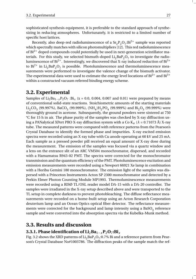
3.3. Results and discussion3.3.1. Phase identification of Li2Ba1−x P2O7:BixFig. 3.2 shows the XRD patterns of Li2BaP2O7:0.7% Bi and a reference pattern from Pear-son’s Crystal Database No#1003786. The diffraction peaks of the sample match the ref-
28 Valence change and VRBE of Bi3+ and Bi2+ in Li2BaP2O7
erence data very well, indicating a phase pure sample. Li2BaP2O7 crystallizes in themonoclinic crystal system with space group C2/c and has a calculated density of 3.51g/cm3 [13]. The Li2BaP2O7 lattice has one crystallographic Ba-site and three differentcrystallographic Li-sites. Considering the ionic radii, the large bismuth ion will mostlikely occupy the bigger Ba-site.
1 0 2 0 3 0 4 0 5 0 6 0 7 0 8 0 9 0
Norm
alized
inten
sity (a
. u.)
L i 2 B a P 2 O 7 : B i ( 0 . 7 m o l % )
2 θ ( d e g )
N o # 1 0 0 3 7 8 6
Figure 3.2: XRD patterns of Li2BaP2O7:0.7% Bi and the reference No#1003786.
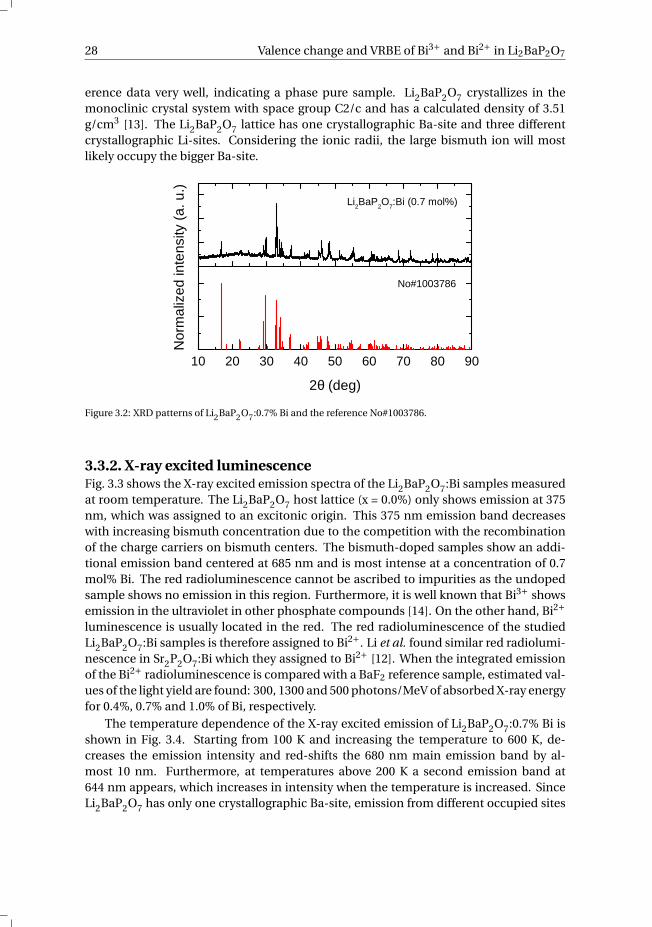
3.3.2. X-ray excited luminescenceFig. 3.3 shows the X-ray excited emission spectra of the Li2BaP2O7:Bi samples measuredat room temperature. The Li2BaP2O7 host lattice (x = 0.0%) only shows emission at 375nm, which was assigned to an excitonic origin. This 375 nm emission band decreaseswith increasing bismuth concentration due to the competition with the recombinationof the charge carriers on bismuth centers. The bismuth-doped samples show an addi-tional emission band centered at 685 nm and is most intense at a concentration of 0.7mol% Bi. The red radioluminescence cannot be ascribed to impurities as the undopedsample shows no emission in this region. Furthermore, it is well known that Bi3+ showsemission in the ultraviolet in other phosphate compounds [14]. On the other hand, Bi2+luminescence is usually located in the red. The red radioluminescence of the studiedLi2BaP2O7:Bi samples is therefore assigned to Bi2+. Li et al. found similar red radiolumi-nescence in Sr2P2O7:Bi which they assigned to Bi2+ [12]. When the integrated emissionof the Bi2+ radioluminescence is compared with a BaF2 reference sample, estimated val-ues of the light yield are found: 300, 1300 and 500 photons/MeV of absorbed X-ray energyfor 0.4%, 0.7% and 1.0% of Bi, respectively.
The temperature dependence of the X-ray excited emission of Li2BaP2O7:0.7% Bi isshown in Fig. 3.4. Starting from 100 K and increasing the temperature to 600 K, de-creases the emission intensity and red-shifts the 680 nm main emission band by al-most 10 nm. Furthermore, at temperatures above 200 K a second emission band at644 nm appears, which increases in intensity when the temperature is increased. SinceLi2BaP2O7 has only one crystallographic Ba-site, emission from different occupied sites
3.3. Results and discussion 29
like in Sr2P2O7:Bi is therefore excluded [15]. The energy difference between the mainemission band and the higher energy sideband is approximately 1000 cm−1 (0.12 eV).The high-energy sideband is therefore attributed to a vibronic transition involving thephosphate stretching vibration which is around 1100 cm−1 in energy. As the temper-ature increases, the transition from the higher vibronic state becomes more probableresulting in the increased intensity of the sideband.
3 0 0 4 0 0 5 0 0 6 0 0 7 0 0 8 0 00 . 0
0 . 2
0 . 4
0 . 6
0 . 8
1 . 0
Int
ensity
(a. u
.)
W a v e l e n g t h ( n m )
1 ) 0 . 0 m o l % 2 ) 0 . 4 m o l % 3 ) 0 . 7 m o l % 4 ) 1 . 0 m o l %
1
2
4
3
Figure 3.3: X-ray excited emission spectra of Li2Ba1−x P2O7 :Bix (x = 0.0, 0.4, 0.7 and 1.0 mol%) measured atroom temperature.
6 0 0 6 5 0 7 0 0 7 5 00 . 0
0 . 5
1 . 0
Inten
sity (a
. u.)
W a v e l e n g t h ( n m )
1 0 0 K 2 0 0 K 3 0 0 K 4 0 0 K 5 0 0 K 6 0 0 K
Figure 3.4: X-ray excited emission spectra of Li2BaP2O7:0.7% Bi as function of temperature.
30 Valence change and VRBE of Bi3+ and Bi2+ in Li2BaP2O7
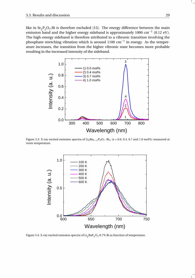
3.3.3. X-ray induced reduction of Bi3+ to Bi2+No Bi3+ or Bi2+ luminescence was observed for the as-prepared Li2BaP2O7:Bi samplesunder UV-vis photon excitation. The absorption spectrum of the Li2BaP2O7:Bi in Fig. 3.5shows the Bi3+ A-band absorption at 250 nm and no Bi2+ related absorption bands, in-dicating that initially only Bi3+ is present in the samples. Probably the Bi3+ emissionis completely quenched as is the case in Ba3(PO4)2 [11]. A possible explanation for thequenching of the Bi3+ luminescence via the formation of Bi3+-Bi3+ pairs is presented inthe next section. The absorption band at 340 nm is observed in both the bismuth dopedand undoped Li2BaP2O7 sample and is related to absorption of defects in the host lattice.
2 0 0 2 5 0 3 0 0 3 5 0 4 0 0 4 5 00 . 0
0 . 1
0 . 2
0 . 3
0 . 4
0 . 5
0 . 6
Kube
lka-M
unk
W a v e l e n g t h ( n m )
1 . 0 m o l % B i U n d o p e d
Figure 3.5: UV – VIS absorption spectra of as-prepared Li2BaP2O7 with 0.0 mol% Bi (undoped) and 1.0 mol %Bi.
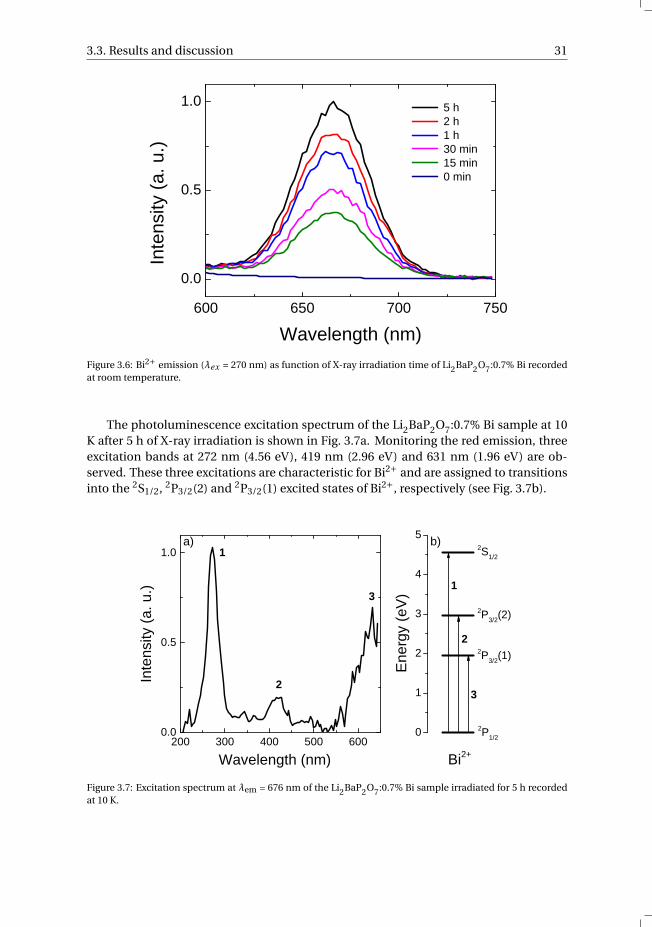
Interestingly, after exposure to X-rays, the red Bi2+ luminescence as seen previouslyin the radioluminescence spectra can be excited optically. The photoluminescence emis-sion spectra of Li2BaP2O7:0.7% Bi usingλex = 270 nm after different X-ray exposure dura-tions are presented in Fig. 3.6. Before X-ray irradiation (0 min), no Bi2+ related emissionis observed. Already after 15 min of X-ray irradiation, an emission band at 667 nm ap-peared which is due to the 2P3/2 → 2P1/2 transition of Bi2+. With longer irradiation time,the luminescence intensity is enhanced and does not seem to saturate even after 5 h ofirradiation time. This indicates that during X-ray exposure the bismuth activator ionsare reduced, i.e. the X-ray induced reduction of Bi3+ to Bi2+. This is similar to the pro-duction of the isoelectronic ions Tl0 and Pb+ using high-energy irradiation reported inthe literature [16, 17]. The intensity of the Bi2+ luminescence increases as the irradiationtime is increased, indicating that the concentration of Bi2+ ions has increased. However,measuring the optical absorption spectrum of the irradiated sample resulted in an iden-tical absorption spectrum as the sample before irradiation, showing only Bi3+ relatedabsorption bands. The amount of Bi2+ formed during X-ray irradiation is probably verylow. The photoluminescence measurements were performed directly after the exposureto X-rays. Measuring the photoluminescence of the samples 12 h after the X-ray expo-sure showed that the Bi2+ photoluminescence had completely faded. This indicates thatthe captured electrons slowly disappear over time.
3.3. Results and discussion 31
6 0 0 6 5 0 7 0 0 7 5 00 . 0
0 . 5
1 . 0
Inten
sity (a
. u.)
W a v e l e n g t h ( n m )
5 h 2 h 1 h 3 0 m i n 1 5 m i n 0 m i n
Figure 3.6: Bi2+ emission (λex = 270 nm) as function of X-ray irradiation time of Li2BaP2O7:0.7% Bi recordedat room temperature.
The photoluminescence excitation spectrum of the Li2BaP2O7:0.7% Bi sample at 10K after 5 h of X-ray irradiation is shown in Fig. 3.7a. Monitoring the red emission, threeexcitation bands at 272 nm (4.56 eV), 419 nm (2.96 eV) and 631 nm (1.96 eV) are ob-served. These three excitations are characteristic for Bi2+ and are assigned to transitionsinto the 2S1/2, 2P3/2(2) and 2P3/2(1) excited states of Bi2+, respectively (see Fig. 3.7b).
2 0 0 3 0 0 4 0 0 5 0 0 6 0 00 . 0
0 . 5
1 . 0
3
3
2
2
1
b )
Inten
sity (a
. u.)
W a v e l e n g t h ( n m )
a ) 1
0
1
2
3
4
5
Energ
y (eV
)
2 S 1 / 2
2 P 3 / 2 ( 2 )
2 P 3 / 2 ( 1 )
B i 2 +
2 P 1 / 2
Figure 3.7: Excitation spectrum at λem = 676 nm of the Li2BaP2O7:0.7% Bi sample irradiated for 5 h recordedat 10 K.
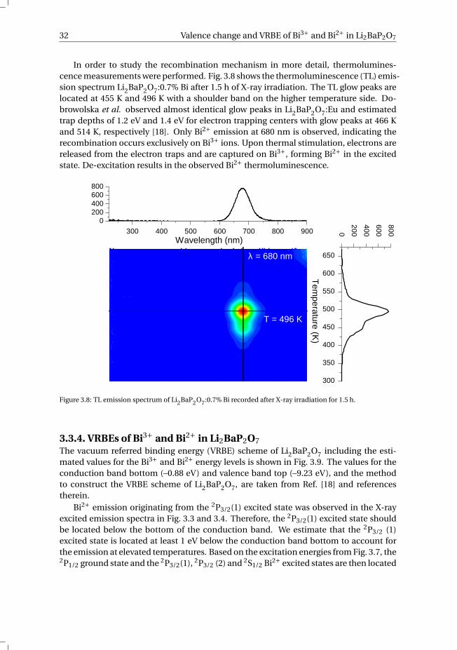
32 Valence change and VRBE of Bi3+ and Bi2+ in Li2BaP2O7
In order to study the recombination mechanism in more detail, thermolumines-cence measurements were performed. Fig. 3.8 shows the thermoluminescence (TL) emis-sion spectrum Li2BaP2O7:0.7% Bi after 1.5 h of X-ray irradiation. The TL glow peaks arelocated at 455 K and 496 K with a shoulder band on the higher temperature side. Do-browolska et al. observed almost identical glow peaks in Li2BaP2O7:Eu and estimatedtrap depths of 1.2 eV and 1.4 eV for electron trapping centers with glow peaks at 466 Kand 514 K, respectively [18]. Only Bi2+ emission at 680 nm is observed, indicating therecombination occurs exclusively on Bi3+ ions. Upon thermal stimulation, electrons arereleased from the electron traps and are captured on Bi3+, forming Bi2+ in the excitedstate. De-excitation results in the observed Bi2+ thermoluminescence.
3 0 0 4 0 0 5 0 0 6 0 0 7 0 0 8 0 0 9 0 0
3 0 03 5 04 0 04 5 05 0 05 5 06 0 06 5 0λ = 6 8 0 n m
T = 4 9 6 K
0200400600800
Temperature (K)
02 0 04 0 06 0 08 0 0
W a v e l e n g t h ( n m )
Figure 3.8: TL emission spectrum of Li2BaP2O7:0.7% Bi recorded after X-ray irradiation for 1.5 h.
3.3.4. VRBEs of Bi3+ and Bi2+ in Li2BaP2O7The vacuum referred binding energy (VRBE) scheme of Li2BaP2O7 including the esti-mated values for the Bi3+ and Bi2+ energy levels is shown in Fig. 3.9. The values for theconduction band bottom (–0.88 eV) and valence band top (–9.23 eV), and the methodto construct the VRBE scheme of Li2BaP2O7, are taken from Ref. [18] and referencestherein.
Bi2+ emission originating from the 2P3/2(1) excited state was observed in the X-rayexcited emission spectra in Fig. 3.3 and 3.4. Therefore, the 2P3/2(1) excited state shouldbe located below the bottom of the conduction band. We estimate that the 2P3/2 (1)excited state is located at least 1 eV below the conduction band bottom to account forthe emission at elevated temperatures. Based on the excitation energies from Fig. 3.7, the2P1/2 ground state and the 2P3/2(1), 2P3/2 (2) and 2S1/2 Bi2+ excited states are then located
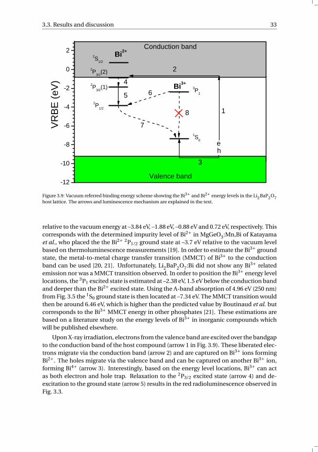
3.3. Results and discussion 33
- 1 2
- 1 0
- 8
- 6
- 4
- 2
0
2
6
87
2 P 3 / 2 ( 1 )
3
3 P 1
1 S 0
2 S 1 / 22 P 3 / 2 ( 2 )
45
2
C o n d u c t i o n b a n dVR
BE (e
V)
V a l e n c e b a n d
B i 2 +
B i 3 +
eh
12 P 1 / 2
Figure 3.9: Vacuum referred binding energy scheme showing the Bi3+ and Bi2+ energy levels in the Li2BaP2O7host lattice. The arrows and luminescence mechanism are explained in the text.
relative to the vacuum energy at –3.84 eV, –1.88 eV, –0.88 eV and 0.72 eV, respectively. Thiscorresponds with the determined impurity level of Bi2+ in MgGeO3:Mn,Bi of Katayamaet al., who placed the the Bi2+ 2P1/2 ground state at –3.7 eV relative to the vacuum levelbased on thermoluminescence measurements [19]. In order to estimate the Bi3+ groundstate, the metal-to-metal charge transfer transition (MMCT) of Bi3+ to the conductionband can be used [20, 21]. Unfortunately, Li2BaP2O7:Bi did not show any Bi3+ relatedemission nor was a MMCT transition observed. In order to position the Bi3+ energy levellocations, the 3P1 excited state is estimated at –2.38 eV, 1.5 eV below the conduction bandand deeper than the Bi2+ excited state. Using the A-band absorption of 4.96 eV (250 nm)from Fig. 3.5 the 1S0 ground state is then located at –7.34 eV. The MMCT transition wouldthen be around 6.46 eV, which is higher than the predicted value by Boutinaud et al. butcorresponds to the Bi3+ MMCT energy in other phosphates [21]. These estimations arebased on a literature study on the energy levels of Bi3+ in inorganic compounds whichwill be published elsewhere.
Upon X-ray irradiation, electrons from the valence band are excited over the bandgapto the conduction band of the host compound (arrow 1 in Fig. 3.9). These liberated elec-trons migrate via the conduction band (arrow 2) and are captured on Bi3+ ions formingBi2+. The holes migrate via the valence band and can be captured on another Bi3+ ion,forming Bi4+ (arrow 3). Interestingly, based on the energy level locations, Bi3+ can actas both electron and hole trap. Relaxation to the 2P3/2 excited state (arrow 4) and de-excitation to the ground state (arrow 5) results in the red radioluminescence observed inFig. 3.3.
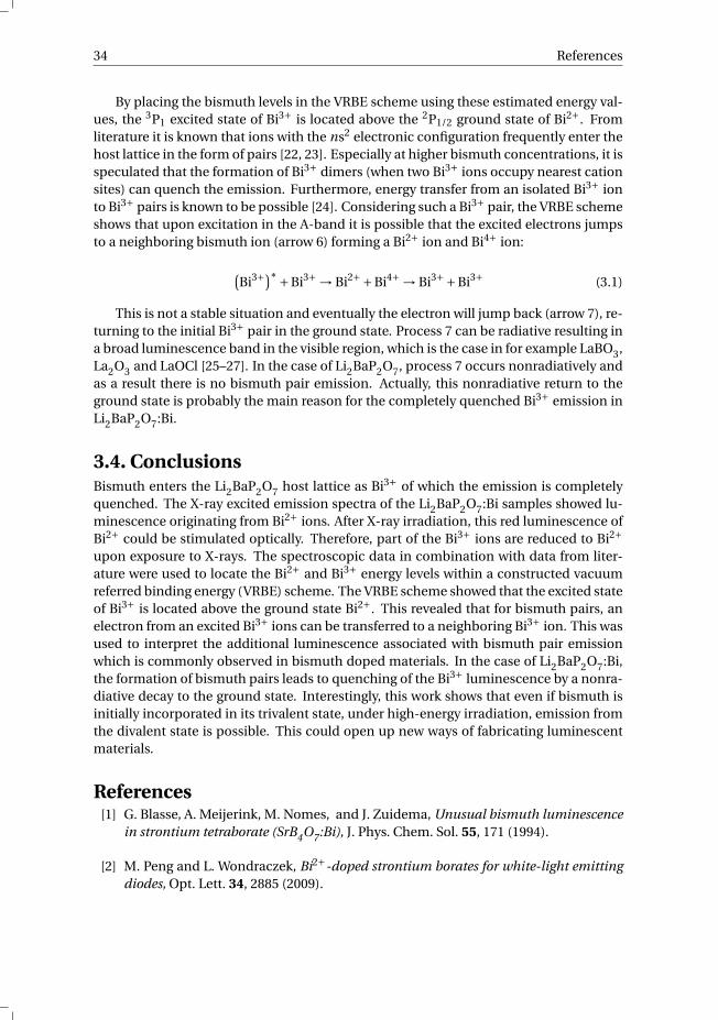
34 References
By placing the bismuth levels in the VRBE scheme using these estimated energy val-ues, the 3P1 excited state of Bi3+ is located above the 2P1/2 ground state of Bi2+. Fromliterature it is known that ions with the ns2 electronic configuration frequently enter thehost lattice in the form of pairs [22, 23]. Especially at higher bismuth concentrations, it isspeculated that the formation of Bi3+ dimers (when two Bi3+ ions occupy nearest cationsites) can quench the emission. Furthermore, energy transfer from an isolated Bi3+ ionto Bi3+ pairs is known to be possible [24]. Considering such a Bi3+ pair, the VRBE schemeshows that upon excitation in the A-band it is possible that the excited electrons jumpsto a neighboring bismuth ion (arrow 6) forming a Bi2+ ion and Bi4+ ion:
(Bi3+)∗+Bi3+ → Bi2++Bi4+ → Bi3++Bi3+ (3.1)
This is not a stable situation and eventually the electron will jump back (arrow 7), re-turning to the initial Bi3+ pair in the ground state. Process 7 can be radiative resulting ina broad luminescence band in the visible region, which is the case in for example LaBO3,La2O3 and LaOCl [25–27]. In the case of Li2BaP2O7, process 7 occurs nonradiatively andas a result there is no bismuth pair emission. Actually, this nonradiative return to theground state is probably the main reason for the completely quenched Bi3+ emission inLi2BaP2O7:Bi.
3.4. ConclusionsBismuth enters the Li2BaP2O7 host lattice as Bi3+ of which the emission is completelyquenched. The X-ray excited emission spectra of the Li2BaP2O7:Bi samples showed lu-minescence originating from Bi2+ ions. After X-ray irradiation, this red luminescence ofBi2+ could be stimulated optically. Therefore, part of the Bi3+ ions are reduced to Bi2+upon exposure to X-rays. The spectroscopic data in combination with data from liter-ature were used to locate the Bi2+ and Bi3+ energy levels within a constructed vacuumreferred binding energy (VRBE) scheme. The VRBE scheme showed that the excited stateof Bi3+ is located above the ground state Bi2+. This revealed that for bismuth pairs, anelectron from an excited Bi3+ ions can be transferred to a neighboring Bi3+ ion. This wasused to interpret the additional luminescence associated with bismuth pair emissionwhich is commonly observed in bismuth doped materials. In the case of Li2BaP2O7:Bi,the formation of bismuth pairs leads to quenching of the Bi3+ luminescence by a nonra-diative decay to the ground state. Interestingly, this work shows that even if bismuth isinitially incorporated in its trivalent state, under high-energy irradiation, emission fromthe divalent state is possible. This could open up new ways of fabricating luminescentmaterials.
References[1] G. Blasse, A. Meijerink, M. Nomes, and J. Zuidema, Unusual bismuth luminescence
in strontium tetraborate (SrB4O7:Bi), J. Phys. Chem. Sol. 55, 171 (1994).
[2] M. Peng and L. Wondraczek, Bi2+-doped strontium borates for white-light emittingdiodes, Opt. Lett. 34, 2885 (2009).
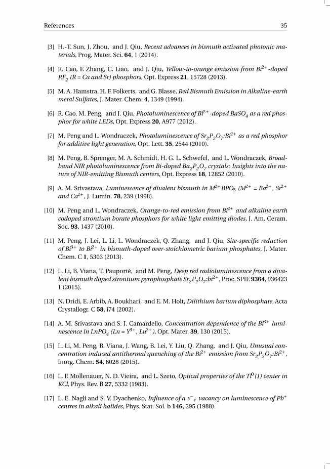
References 35
[3] H.-T. Sun, J. Zhou, and J. Qiu, Recent advances in bismuth activated photonic ma-terials, Prog. Mater. Sci. 64, 1 (2014).
[4] R. Cao, F. Zhang, C. Liao, and J. Qiu, Yellow-to-orange emission from Bi2+-dopedRF2 (R = Ca and Sr) phosphors, Opt. Express 21, 15728 (2013).
[5] M. A. Hamstra, H. F. Folkerts, and G. Blasse, Red Bismuth Emission in Alkaline-earthmetal Sulfates, J. Mater. Chem. 4, 1349 (1994).
[6] R. Cao, M. Peng, and J. Qiu, Photoluminescence of Bi2+-doped BaSO4 as a red phos-phor for white LEDs, Opt. Express 20, A977 (2012).
[7] M. Peng and L. Wondraczek, Photoluminescence of Sr2P2O7:Bi2+ as a red phosphorfor additive light generation, Opt. Lett. 35, 2544 (2010).
[8] M. Peng, B. Sprenger, M. A. Schmidt, H. G. L. Schwefel, and L. Wondraczek, Broad-band NIR photoluminescence from Bi-doped Ba2P2O7 crystals: Insights into the na-ture of NIR-emitting Bismuth centers, Opt. Express 18, 12852 (2010).
[9] A. M. Srivastava, Luminescence of divalent bismuth in M2+BPO5 (M2+ = Ba2+, Sr2+and Ca2+, J. Lumin. 78, 239 (1998).
[10] M. Peng and L. Wondraczek, Orange-to-red emission from Bi2+ and alkaline earthcodoped strontium borate phosphors for white light emitting diodes, J. Am. Ceram.Soc. 93, 1437 (2010).
[11] M. Peng, J. Lei, L. Li, L. Wondraczek, Q. Zhang, and J. Qiu, Site-specific reductionof Bi3+ to Bi2+ in bismuth-doped over-stoichiometric barium phosphates, J. Mater.Chem. C 1, 5303 (2013).
[12] L. Li, B. Viana, T. Pauporté, and M. Peng, Deep red radioluminescence from a diva-lent bismuth doped strontium pyrophosphate Sr2P2O7:bi2+, Proc. SPIE 9364, 9364231 (2015).
[13] N. Dridi, E. Arbib, A. Boukhari, and E. M. Holt, Dilithium barium diphosphate, ActaCrystallogr. C 58, i74 (2002).
[14] A. M. Srivastava and S. J. Camardello, Concentration dependence of the Bi3+ lumi-nescence in LnPO4 (Ln = Y3+, Lu3+), Opt. Mater. 39, 130 (2015).
[15] L. Li, M. Peng, B. Viana, J. Wang, B. Lei, Y. Liu, Q. Zhang, and J. Qiu, Unusual con-centration induced antithermal quenching of the Bi2+ emission from Sr2P2O7:Bi2+,Inorg. Chem. 54, 6028 (2015).
[16] L. F. Mollenauer, N. D. Vieira, and L. Szeto, Optical properties of the Tl0(1) center inKCl, Phys. Rev. B 27, 5332 (1983).
[17] L. E. Nagli and S. V. Dyachenko, Influence of a v−c vacancy on luminescence of Pb+centres in alkali halides, Phys. Stat. Sol. b 146, 295 (1988).
36 References
[18] A. Dobrowolska, A. J. J. Bos, and P. Dorenbos, Charge carrier storage properties andthe vacuum referred binding energy scheme for Li2BaP2O7:Ln (Ln=Ce, Eu, Tb, Yb), J.Lumin. 170, 497 (2016).
[19] Y. Katayama, J. Ueda, and S. Tanabe, Effect of Bi2O3 doping on persistent lumines-cence of MgGeO3:Mn2+ phosphor, Opt. Mater. Express 4, 613 (2014).
[20] P. Boutinaud and E. Cavalli, Predicting the metal-to-metal charge transfer in closed-shell transition metal oxides doped with Bi3+ or Pb2+, Chem. Phys. Lett. 503, 239(2011).
[21] P. Boutinaud, Revisiting the spectroscopy of the Bi3+ ion in oxide compounds, Inorg.Chem. 52, 6028 (2013).
[22] A. M. Srivastava, On the luminescence of Bi3+ in the pyrochlore Y2Sn2O7, Mater. Res.Bull 37, 745 (2002).
[23] A. A. Setlur and A. M. Srivastava, The nature of Bi3+ luminescence in garnet hosts,Opt. Mater. 29, 410 (2006).
[24] H. Zhiran and G. Blasse, Energy transfer phenomena in luminescent materials basedon GdB3O6, Mater. Chem. Phys. 12, 257 (1985).
[25] A. Wolfert, E. W. J. L. Oomen, and G. Blasse, Host lattice dependence of the Bi3+luminescence in orthoborates LnBO3 (with Ln = Sc, Y, La, Gd or Lu), J. Solid StateChem. 59, 280 (1985).
[26] A. M. van de Craats and G. Blasse, The quenching of bismuth(III) luminescence inyttrium oxide (Y2O3), Chem. Phys. Lett. 243, 559 (1995).
[27] A. Wolfert and G. Blasse, Luminescence of the Bi3+ ion in compounds LnOCl (Ln =La, Y, Gd), Mater. Res. Bull. 19, 67 (1984).
4Luminescence and charge carrier
trapping in YPO4:Bi
YPO4 doped with Bi3+ and/or Tb3+ samples were prepared in air. X-ray excited lumines-cence measurements showed emission from isolated Bi3+ and Bi-pairs, and also emis-sion from Bi2+ was observed. Based on the obtained spectroscopic data, the electronbinding energies in the ground and excited states of Bi3+ and Bi2+ were placed insidethe vacuum referred binding energy (VRBE) scheme, and this was used to explain theluminescence of bismuth doped YPO4. The VRBE scheme and additional thermolumi-nescence glow curves show that bismuth can act both as electron and as hole trap inYPO4.
This chapter is based on the publication: R. H. P. Awater, L. C. Niemeijer-Berghuijs andP. Dorenbos, “Luminescence and charge carrier trapping in YPO4:Bi”, Optical Materials66 (2017), 351.
37
38 4. Luminescence and charge carrier trapping in YPO4:Bi
4.1. IntroductionBi3+ is a well-studied activator and sensitizer for luminescent materials [1]. The Bi3+ ionhas the 6s2 outer electron configuration, and optical transitions to three 6s6p excitedstates, labeled as A-, B- and C-bands, can be observed. Also a metal-to-metal chargetransfer (MMCT) from the Bi3+ ground state to the host conduction band (CB) is com-monly observed. In addition to the characteristic A-band emission, a lower energy emis-sion band is frequently reported (see column 8 in Table 5.1). There is still controversyabout the origin of this lower energy emission band. In a recent evaluation, Boutinaudtentatively assigned it to CB → Bi3+/4+ CT luminescence [2]. Alternatively, Srivastava as-signed the additional emission band in Y2Sn2O7 and GdAlO3 to emission from Bi3+–Bi3+pairs or clusters [3, 4]. Also Wolfert et al. proposed in the 1980s that bismuth pairs canbe the origin of the additional emission observed in Bi3+-doped rare earth borates andoxychlorides [5, 6].
In 1994, Blasse et al. confirmed the luminescence of the unique divalent bismuthoxidation state in SrB4O7 and BaSO4 [7, 8]. Later, Bi2+ luminescence was also reportedin alkaline-earth fluorides, sulfates, phosphates and borates for white-light LED applica-tions [9–13]. Divalent bismuth shows luminescence in the orange-red to infrared part ofthe spectrum. With excitation bands in the near ultraviolet (NUV) and blue, Bi2+-dopedphosphors are ideal to be used in combination with an InGaN LED in order to makewhite light LEDs [14]. Furthermore, the red radioluminescence reported for Sr2P2O7:Bi2+spectrally matches with the sensitivity of silicon-based semiconductor detectors, mak-ing Bi2+ a promising activator ion for the next-generation long wavelength emitting scin-tillator materials [15]. The difficulty is to stabilize Bi2+ in the host lattice. Usually, areducing atmosphere is required. Peng et al. showed that Bi2+ can also be stabilizedin over-stoichiometric barium phosphates [16]. In chapter 3 it was shown that X-rayinduced reduction of Bi3+ to Bi2+ is possible in Li2BaP2O7:Bi. In this chapter, radiolu-minescence of divalent bismuth originating from bismuth ions doped on trivalent hostlattice sites is shown.
In order to gain more insight in the trapping and luminescence properties of bis-muth, we selected YPO4:Bi as our compound of interest. YPO4 is a wide band gap com-pound with only one crystallographic Y-site where Bi3+ can be situated. Its electronicstructure is well-established from lanthanide spectroscopy and also the spectroscopyof YPO4:Bi has been discussed in literature [17–19]. In order to estimate the VRBE in theBi2+ ground state in YPO4, thermoluminescence measurements of co-doped YPO4:Bi,Tbwere performed. We discovered that bismuth acts as both electron and hole trap, andthat in the case of YPO4, the hole is trapped more shallower than the electron.
4.2. ExperimentalSamples of YPO4 doped with varying amounts of Bi3+ and/or Tb3+ were prepared us-ing conventional solid-state sintering. Stoichiometric amounts of the starting materialsY2O3 (99.99%), (NH4)H2PO4 (99.999%), Bi2O3 (99.999%) and Tb2O3 (99.999%) were thor-oughly ground in acetone. The ground powders were first sintered at 400 °C for 10 h inair. After an intermediate grinding step in acetone, the samples were sintered at 1400°C for 4 h in air. X-ray diffraction was used to check the phase purity of the samples us-
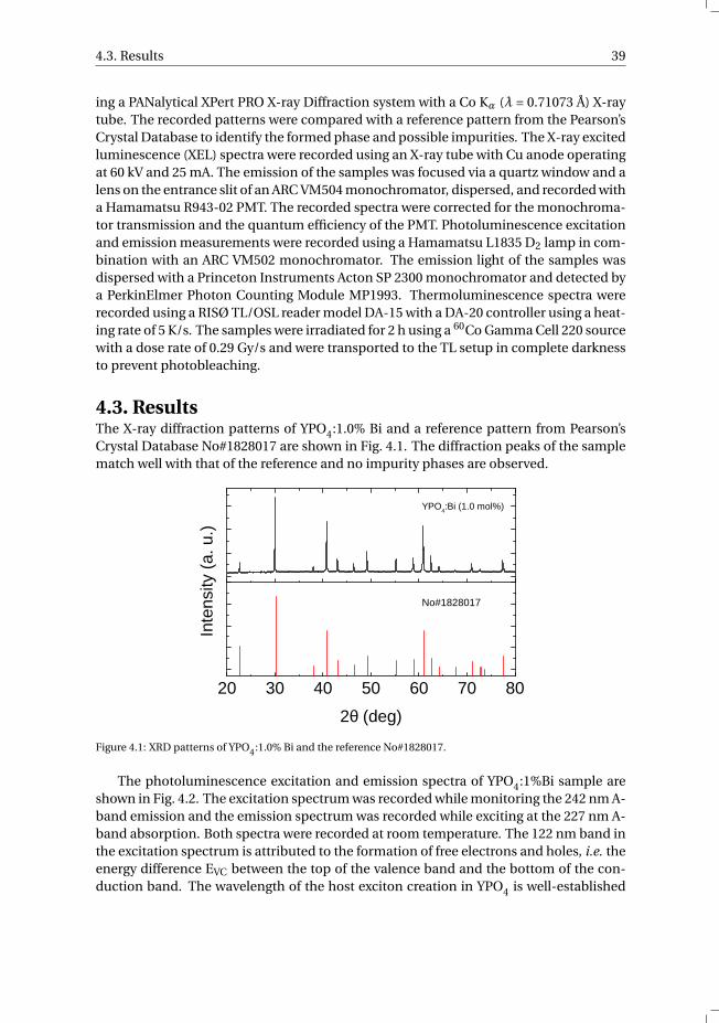
4.3. Results 39
ing a PANalytical XPert PRO X-ray Diffraction system with a Co Kα (λ = 0.71073 Å) X-raytube. The recorded patterns were compared with a reference pattern from the Pearson’sCrystal Database to identify the formed phase and possible impurities. The X-ray excitedluminescence (XEL) spectra were recorded using an X-ray tube with Cu anode operatingat 60 kV and 25 mA. The emission of the samples was focused via a quartz window and alens on the entrance slit of an ARC VM504 monochromator, dispersed, and recorded witha Hamamatsu R943-02 PMT. The recorded spectra were corrected for the monochroma-tor transmission and the quantum efficiency of the PMT. Photoluminescence excitationand emission measurements were recorded using a Hamamatsu L1835 D2 lamp in com-bination with an ARC VM502 monochromator. The emission light of the samples wasdispersed with a Princeton Instruments Acton SP 2300 monochromator and detected bya PerkinElmer Photon Counting Module MP1993. Thermoluminescence spectra wererecorded using a RISØ TL/OSL reader model DA-15 with a DA-20 controller using a heat-ing rate of 5 K/s. The samples were irradiated for 2 h using a 60Co Gamma Cell 220 sourcewith a dose rate of 0.29 Gy/s and were transported to the TL setup in complete darknessto prevent photobleaching.
4.3. ResultsThe X-ray diffraction patterns of YPO4:1.0% Bi and a reference pattern from Pearson’sCrystal Database No#1828017 are shown in Fig. 4.1. The diffraction peaks of the samplematch well with that of the reference and no impurity phases are observed.
2 0 3 0 4 0 5 0 6 0 7 0 8 0
Inten
sity (a
. u.)
Y P O 4 : B i ( 1 . 0 m o l % )
2 θ ( d e g )
N o # 1 8 2 8 0 1 7
Figure 4.1: XRD patterns of YPO4:1.0% Bi and the reference No#1828017.
The photoluminescence excitation and emission spectra of YPO4:1%Bi sample areshown in Fig. 4.2. The excitation spectrum was recorded while monitoring the 242 nm A-band emission and the emission spectrum was recorded while exciting at the 227 nm A-band absorption. Both spectra were recorded at room temperature. The 122 nm band inthe excitation spectrum is attributed to the formation of free electrons and holes, i.e. theenergy difference EVC between the top of the valence band and the bottom of the con-duction band. The wavelength of the host exciton creation in YPO4 is well-established
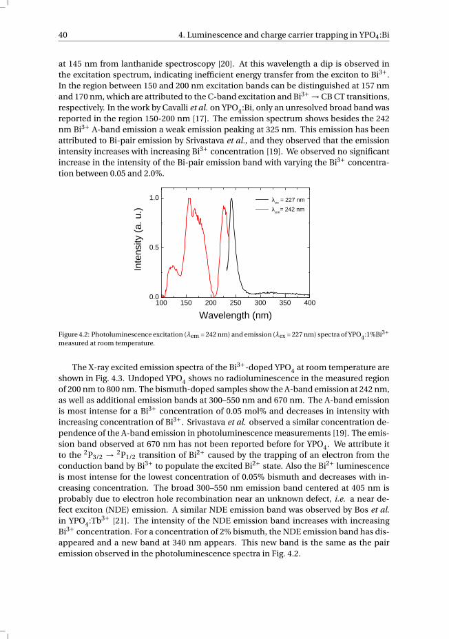
40 4. Luminescence and charge carrier trapping in YPO4:Bi
at 145 nm from lanthanide spectroscopy [20]. At this wavelength a dip is observed inthe excitation spectrum, indicating inefficient energy transfer from the exciton to Bi3+.In the region between 150 and 200 nm excitation bands can be distinguished at 157 nmand 170 nm, which are attributed to the C-band excitation and Bi3+ → CB CT transitions,respectively. In the work by Cavalli et al. on YPO4:Bi, only an unresolved broad band wasreported in the region 150-200 nm [17]. The emission spectrum shows besides the 242nm Bi3+ A-band emission a weak emission peaking at 325 nm. This emission has beenattributed to Bi-pair emission by Srivastava et al., and they observed that the emissionintensity increases with increasing Bi3+ concentration [19]. We observed no significantincrease in the intensity of the Bi-pair emission band with varying the Bi3+ concentra-tion between 0.05 and 2.0%.
1 0 0 1 5 0 2 0 0 2 5 0 3 0 0 3 5 0 4 0 00 . 0
0 . 5
1 . 0
Inten
sity (a
. u.)
W a v e l e n g t h ( n m )
λ e x = 2 2 7 n m λ e m = 2 4 2 n m
Figure 4.2: Photoluminescence excitation (λem = 242 nm) and emission (λex = 227 nm) spectra of YPO4:1%Bi3+measured at room temperature.
The X-ray excited emission spectra of the Bi3+-doped YPO4 at room temperature areshown in Fig. 4.3. Undoped YPO4 shows no radioluminescence in the measured regionof 200 nm to 800 nm. The bismuth-doped samples show the A-band emission at 242 nm,as well as additional emission bands at 300–550 nm and 670 nm. The A-band emissionis most intense for a Bi3+ concentration of 0.05 mol% and decreases in intensity withincreasing concentration of Bi3+. Srivastava et al. observed a similar concentration de-pendence of the A-band emission in photoluminescence measurements [19]. The emis-sion band observed at 670 nm has not been reported before for YPO4. We attribute itto the 2P3/2 → 2P1/2 transition of Bi2+ caused by the trapping of an electron from theconduction band by Bi3+ to populate the excited Bi2+ state. Also the Bi2+ luminescenceis most intense for the lowest concentration of 0.05% bismuth and decreases with in-creasing concentration. The broad 300–550 nm emission band centered at 405 nm isprobably due to electron hole recombination near an unknown defect, i.e. a near de-fect exciton (NDE) emission. A similar NDE emission band was observed by Bos et al.in YPO4:Tb3+ [21]. The intensity of the NDE emission band increases with increasingBi3+ concentration. For a concentration of 2% bismuth, the NDE emission band has dis-appeared and a new band at 340 nm appears. This new band is the same as the pairemission observed in the photoluminescence spectra in Fig. 4.2.
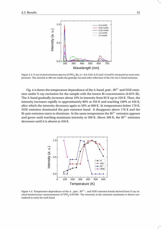
4.3. Results 41
2 5 0 3 5 0 4 5 0 5 5 0 6 5 0 7 5 00 . 0
0 . 5
1 . 0
Inten
sity (a
. u.)
W a v e l e n g t h ( n m )
0 . 0 m o l % 0 . 0 5 m o l % 0 . 2 5 m o l % 1 . 0 m o l % 2 . 0 m o l %
*
Figure 4.3: X-ray excited emission spectra of YPO4:Bix (x = 0.0, 0.05, 0.25 and 1.0 mol%) measured at room tem-perature. The asterisk at 480 nm marks the grating’s second order reflection of the 242 nm A-band emission.
Fig. 4.4 shows the temperature dependence of the A-band, pair-, Bi2+ and NDE emis-sion under X-ray excitation for the sample with the lowest Bi concentration (0.05% Bi).The A-band gradually increases about 10% in intensity from 85 K up to 250 K. Then, theintensity increases rapidly to approximately 80% at 350 K and reaching 100% at 450 K,after which the intensity decreases again to 50% at 600 K. At temperatures below 170 K,NDE emission dominated the pair emission band. It disappears above 170 K and theBi-pair emission starts to dominate. At the same temperature the Bi2+ emission appearsand grows until reaching maximum intensity at 300 K. Above 300 K, the Bi2+ emissiondecreases until it is absent at 450 K.
0 1 0 0 2 0 0 3 0 0 4 0 0 5 0 0 6 0 00 . 0
0 . 5
1 . 0
Inten
sity (a
. u.)
T e m p e r a t u r e ( K )
A p a i r B i 2 +
N D E
Figure 4.4: Temperature dependence of the A-, pair-, Bi2+-, and NDE emission bands derived from X-ray ex-cited luminescence measurements of YPO4:0.05%Bi. The intensity at the emission maximum is shown nor-malized to unity for each band.
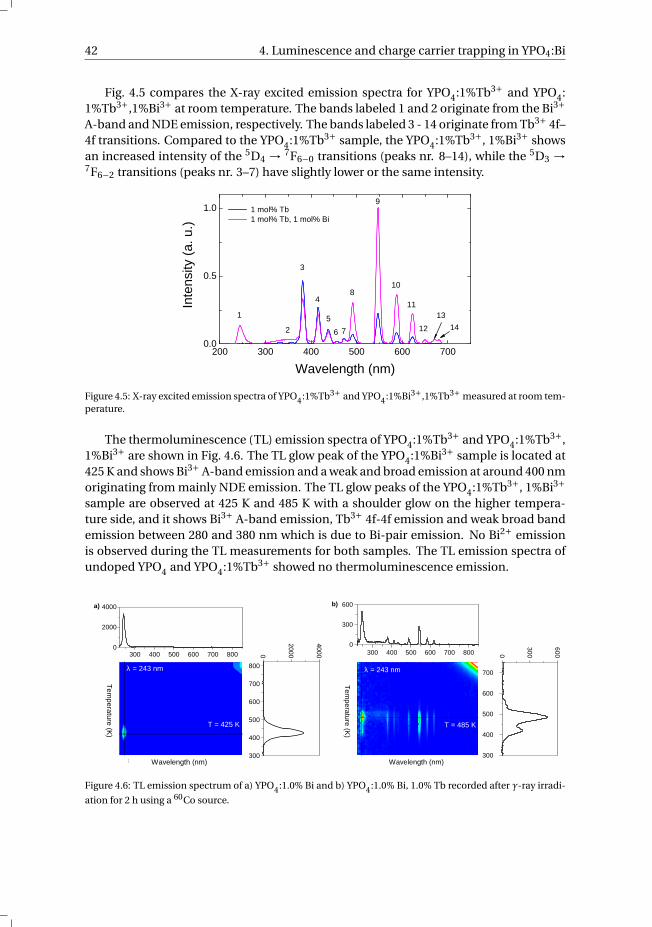
42 4. Luminescence and charge carrier trapping in YPO4:Bi
Fig. 4.5 compares the X-ray excited emission spectra for YPO4:1%Tb3+ and YPO4:1%Tb3+,1%Bi3+ at room temperature. The bands labeled 1 and 2 originate from the Bi3+A-band and NDE emission, respectively. The bands labeled 3 - 14 originate from Tb3+ 4f–4f transitions. Compared to the YPO4:1%Tb3+ sample, the YPO4:1%Tb3+, 1%Bi3+ showsan increased intensity of the 5D4 → 7F6−0 transitions (peaks nr. 8–14), while the 5D3 →7F6−2 transitions (peaks nr. 3–7) have slightly lower or the same intensity.
2 0 0 3 0 0 4 0 0 5 0 0 6 0 0 7 0 00 . 0
0 . 5
1 . 0
1 41 3
1 2
1 11 08
9
765
4
2
3
Int
ensity
(a. u
.)
W a v e l e n g t h ( n m )
1 m o l % T b 1 m o l % T b , 1 m o l % B i
1
Figure 4.5: X-ray excited emission spectra of YPO4:1%Tb3+ and YPO4:1%Bi3+,1%Tb3+ measured at room tem-perature.
The thermoluminescence (TL) emission spectra of YPO4:1%Tb3+ and YPO4:1%Tb3+,1%Bi3+ are shown in Fig. 4.6. The TL glow peak of the YPO4:1%Bi3+ sample is located at425 K and shows Bi3+ A-band emission and a weak and broad emission at around 400 nmoriginating from mainly NDE emission. The TL glow peaks of the YPO4:1%Tb3+, 1%Bi3+sample are observed at 425 K and 485 K with a shoulder glow on the higher tempera-ture side, and it shows Bi3+ A-band emission, Tb3+ 4f-4f emission and weak broad bandemission between 280 and 380 nm which is due to Bi-pair emission. No Bi2+ emissionis observed during the TL measurements for both samples. The TL emission spectra ofundoped YPO4 and YPO4:1%Tb3+ showed no thermoluminescence emission.
3 0 0 4 0 0 5 0 0 6 0 0 7 0 0 8 0 0
3 0 0
4 0 0
5 0 0
6 0 0
7 0 0
8 0 0
2 4 3
4 2 5
W a v e l e n g t h ( n m )
λ = 2 4 3 n m
T = 4 2 5 K
Temperature (K)
a )
0
2000
40000
2 0 0 0
4 0 0 0
3 0 0 4 0 0 5 0 0 6 0 0 7 0 0 8 0 0
3 0 0
4 0 0
5 0 0
6 0 0
7 0 0
2 4 4 . 1
4 8 5
Temperature (K)
W a v e l e n g t h ( n m )
λ = 2 4 3 n m
T = 4 8 5 K
0
300
600
b )
0
3 0 0
6 0 0
Figure 4.6: TL emission spectrum of a) YPO4:1.0% Bi and b) YPO4:1.0% Bi, 1.0% Tb recorded after γ-ray irradi-
ation for 2 h using a 60Co source.
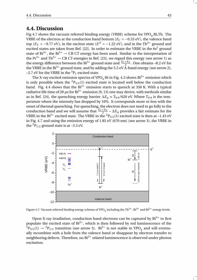
4.4. Discussion 43
4.4. DiscussionFig 4.7 shows the vacuum referred binding energy (VRBE) scheme for YPO4:Bi,Tb. TheVRBE of the electron at the conduction band bottom (EC =−0.53 eV), the valence bandtop (EV = −9.77 eV), in the exciton state (E X = −1.22 eV), and in the Tb3+ ground andexcited states are taken from Ref. [22]. In order to estimate the VRBE in the 6s2 groundstate of Bi3+, the Bi3+ → CB CT energy has been used. Similar to the interpretation ofthe Pr3+ and Tb3+ → CB CT-energies in Ref. [23], we regard this energy (see arrow 1) asthe energy difference between the Bi3+ ground state and EC+EX
2 . One obtains –8.2 eV forthe VRBE in the Bi3+ ground state, and by adding the 5.5 eV A-band energy (see arrow 2),–2.7 eV for the VRBE in the 3P1 excited state.
The X-ray excited emission spectra of YPO4:Bi in Fig. 4.3 shows Bi2+ emission whichis only possible when the 2P3/2(1) excited state is located well below the conductionband. Fig. 4.4 shows that the Bi2+ emission starts to quench at 350 K. With a typicalradiative life time of 20 µs for Bi2+ emission [9, 13] one may derive, with methods similaras in Ref. [24], the quenching energy barrier ∆Eq ≈ T0.9/620 eV. Where T0.9 is the tem-perature where the intensity has dropped by 10%. It corresponds more or less with theonset of thermal quenching. For quenching, the electron does not need to go fully to theconduction band and we will assume that EC+EX
2 −∆Eq provides a fair estimate for theVRBE in the Bi2+ excited state. The VRBE in the 2P3/2(1) excited state is then at –1.43 eVin Fig. 4.7 and using the emission energy of 1.85 eV (670 nm) (see arrow 3), the VRBE inthe 2P1/2 ground state is at –3.3 eV.
- 1 2
- 1 0
- 8
- 6
- 4
- 2
0
2
3
4
1
V a l e n c e b a n d
C o n d u c t i o n b a n d
B i 2 +
B i 3 +
5 d [ L S ]
5 D 3
VRBE
(eV)
T b 3 +
E X
5 D 4
5 d [ H S ]
2
1.85 e
V
5.5 eV
A-ba
nd
7.3 eV
MMC
T
3.65 e
V pair
emiss
ion
Figure 4.7: Vacuum referred binding energy scheme of YPO4 including the Tb3+, Bi3+ and Bi2+ energy levels.
Upon X-ray irradiation, conduction band electrons can be captured by Bi3+ to firstpopulate the excited state of Bi2+, which is then followed by red luminescence of the2P3/2(1) → 2P1/2 transition (see arrow 3). Bi2+ is not stable in YPO4 and will eventu-ally recombine with a hole from the valence band or disappear by electron transfer toneighboring defects. Therefore, no Bi2+ related luminescence is observed under photonexcitation.
44 4. Luminescence and charge carrier trapping in YPO4:Bi
The XEL spectrum of YPO4:Bi,Tb in Fig. 4.5 shows enhanced emission intensity fromthe Tb3+ 5D4 → 7F7−0 transitions as compared to that of single-doped YPO4:Tb. In sin-gle doped YPO4:Tb3+, the Tb3+ ions can be excited by first trapping a hole and later anelectron, or by means of e-h pair capture, or energy transfer from the exciton or NDEstate. In the presence of Bi3+ even more excitation paths are envisaged. Angiuli et al. al-ready showed that Bi3+ → Tb3+ energy transfer occurs in YPO4:Bi,Tb [25]. Probably alsoTb4+-Bi2+ pairs can be formed during X-ray exposure, and electron back transfer fromBi2+ may then also generate Tb3+ emission. Possibly, the electron transfer from Bi to Tbis more likely to populate the 5D4 level.
In the TL emission spectrum of YPO4:1%Bi in Fig. 4.6, a single glow peak is observedat 425 K which shows Bi3+ A-band emission at 243 nm. This indicates that the lumi-nescence occurs from either electron capture on Bi4+ or from hole capture on Bi2+. Ac-cording to Fig. 4.7, Bi3+ can act as a 1.57 eV deep hole trap to form Bi4+ but also as a2.97 eV deep electron trap to form Bi2+. The hole will be released earlier from its trapthan the electron. Besides the Bi2+/3+ electron trap, other unknown host related electrontraps may be present. Electron release from these unknown defects would generate be-sides Bi3+ emission (recombination on Bi4+) also Bi2+ emission (recombination on Bi3+).Since no Bi2+ emission is observed, the Bi3+ emission of the 425 K glow is attributed toBi4+ hole release that recombines with Bi2+. Supporting evidence is the absence of anythermoluminescence glow for YPO4:Tb3+. Tb3+ can only capture holes to form Tb4+ andonly liberated electrons can recombine at Tb4+. The formation of Bi4+ may seem strangesince it is regarded as chemically unstable. Indeed during synthesis Bi4+ is never formed,however, since the Bi3+ ground state is above the valence band it can trap a hole to formBi4+ as a meta-stable defect.
The TL emission spectrum of YPO4:Bi,Tb in Fig. 4.6 shows both Bi3+ A-band andTb3+ 4f-4f glow at 425 K and 485 K. We attribute the observed Tb3+ glow at 425 K to holerelease from Bi4+ and recombination on Bi2+ followed by Bi3+ → Tb3+ energy transfer.In the VRBE scheme Tb3+ is predicted to act as a 2.1 eV deep hole trap which is 0.5 eVdeeper than that by Bi3+. We therefore attribute the 485 K glow peak to hole release fromTb4+, which recombines with the Bi2+ electron trap, producing Bi3+ A-band glow andTb3+ glow via energy transfer. Also weak Bi–Bi pair emission near 320 nm is visible at485 K. Apparently, once the hole on Tb4+ is released it can migrate towards an electrontrapped in a Bi–Bi pair resulting in the 3.65 eV pair emission. The rather low probabilityof this recombination mechanism accounts for its weak intensity. In the case of YPO4:Bi,the pair emission is probably dominated by the NDE emission observed at around 400nm.
4.5. ConclusionsX-ray excited emission spectra of YPO4:Bi samples showed luminescence originatingfrom Bi3+, Bi2+ and Bi-pair emission. This chapter showed that characteristic red radi-oluminescence of Bi2+ is observed in YPO4 doped with Bi3+. Such type of radiolumine-cence may be utilized as red emitting scintillator material. The spectroscopic data onBi3+ and Bi2+ was used to determine the VRBE of the electron in the ground and excitedstates of the Bi2+ and Bi3+. The VRBE scheme, together with data from thermolumines-cence glow curves showed that Bi3+ can act as both electron and hole trap in YPO4.
References 45
References[1] G. Blasse and A. Bril, Investigations of Bi3+-activated phosphors, J. Chem. Phys. 48,
217 (1968).
[2] P. Boutinaud, Revisiting the spectroscopy of the Bi3+ ion in oxide compounds, Inorg.Chem. 52, 6028 (2013).
[3] A. M. Srivastava, On the luminescence of Bi3+ in the pyrochlore Y2Sn2O7, Mater. Res.Bull 37, 745 (2002).
[4] A. M. Srivastava and H. A. Comanzo, The ultraviolet and visible luminescence of Bi3+in the orthorhombic perovskite, GdAlO3, Opt. Mater. 63, 118 (2017).
[5] A. Wolfert, E. W. J. L. Oomen, and G. Blasse, Host lattice dependence of the Bi3+luminescence in orthoborates LnBO3 (with Ln = Sc, Y, La, Gd or Lu), J. Solid StateChem. 59, 280 (1985).
[6] A. Wolfert and G. Blasse, Luminescence of the Bi3+ ion in compounds LnOCl (Ln =La, Y, Gd), Mater. Res. Bull. 19, 67 (1984).
[7] G. Blasse, A. Meijerink, M. Nomes, and J. Zuidema, Unusual bismuth luminescencein strontium tetraborate (SrB4O7:Bi), J. Phys. Chem. Sol. 55, 171 (1994).
[8] M. A. Hamstra, H. F. Folkerts, and G. Blasse, Red Bismuth Emission in Alkaline-earthmetal Sulfates, J. Mater. Chem. 4, 1349 (1994).
[9] R. Cao, F. Zhang, C. Liao, and J. Qiu, Yellow-to-orange emission from Bi2+-dopedRF2 (R = Ca and Sr) phosphors, Opt. Express 21, 15728 (2013).
[10] R. Cao, M. Peng, and J. Qiu, Photoluminescence of Bi2+-doped BaSO4 as a red phos-phor for white LEDs, Opt. Express 20, A977 (2012).
[11] M. Peng and L. Wondraczek, Photoluminescence of Sr2P2O7:Bi2+ as a red phosphorfor additive light generation, Opt. Lett. 35, 2544 (2010).
[12] A. M. Srivastava, Luminescence of divalent bismuth in M2+BPO5 (M2+ = Ba2+, Sr2+and Ca2+, J. Lumin. 78, 239 (1998).
[13] M. Peng and L. Wondraczek, Bi2+-doped strontium borates for white-light emittingdiodes, Opt. Lett. 34, 2885 (2009).
[14] L. Li, M. Peng, B. Viana, J. Wang, B. Lei, Y. Liu, Q. Zhang, and J. Qiu, Unusual con-centration induced antithermal quenching of the Bi2+ emission from Sr2P2O7:Bi2+,Inorg. Chem. 54, 6028 (2015).
[15] L. Li, B. Viana, T. Pauporté, and M. Peng, Deep red radioluminescence from a diva-lent bismuth doped strontium pyrophosphate Sr2P2O7:bi2+, Proc. SPIE 9364, 9364231 (2015).
46 References
[16] M. Peng, J. Lei, L. Li, L. Wondraczek, Q. Zhang, and J. Qiu, Site-specific reductionof Bi3+ to Bi2+ in bismuth-doped over-stoichiometric barium phosphates, J. Mater.Chem. C 1, 5303 (2013).
[17] E. Cavalli, F. Angiuli, F. Mezzadri, M. Trevisani, M. Bettinelli, P. Boutinaud, and M. G.Brik, Tunable luminescence of Bi3+-doped YPx V1−x O4 (0 ≤ x ≤ 1), J. Phys.: Condens.Matter 26, 385503 (2014).
[18] T. Jüstel, P. Huppertz, W. Mayr, and D. U. Wiechert, Temperature-dependent spectraof YPO4:Me (Me = Ce, Pr, Nd, Bi), J. Lumin. 106, 225 (2004).
[19] A. M. Srivastava and S. J. Camardello, Concentration dependence of the Bi3+ lumi-nescence in LnPO4 (Ln = Y3+, Lu3+), Opt. Mater. 39, 130 (2015).
[20] P. Dorenbos, A. J. J. Bos, and N. R. J. Poolton, Carrier recombination processes anddivalent lanthanide spectroscopy in YPO4:Ce3+;L3+ L=Sm,Dy,Tm), Phys. Rev. B 82,195127 (2010).
[21] A. Bos, P. Dorenbos, A. Bessiere, A. Lecointre, M. Bedu, M. Bettinelli, and F. Pic-cinelli, Study of TL glow curves of YPO4 double doped with lanthanide ions, Radiat.Meas. 46, 1410 (2011).
[22] P. Dorenbos, The electronic level structure of lanthanide impurities in REPO4,REBO3, REAlO3, and RE2O3 (RE = La, Gd, Y, Lu, Sc) compounds, J. Phys.: Condens.Matter 25, 225501 (2013).
[23] P. Dorenbos, A. H. Krumpel, E. van der Kolk, P. Boutinaud, and E. Cavalli, Lan-thanide level location in transition metal complex compounds, Opt. Mater. 32, 1681(2010).
[24] P. Dorenbos, Thermal quenching of Eu2+ 5d–4f luminescence in inorganic com-pounds, J. Phys.: Condens. Matter 17, 8103 (2005).
[25] F. Angiuli, E. Cavalli, and A. Belletti, Synthesis and spectroscopic characterization ofYPO4 activated with Tb3+ and effect of Bi3+ co-doping on the luminescence proper-ties, J. Solid State Chem. 192, 289 (2012).
5The Bi3+ 6s and 6p electron bindingenergies in relation to the chemical
environment of inorganic compounds
This chapter provides an overview and interpretation of the spectroscopic data of theBi3+ activator ion in 117 different inorganic compounds. The energies of the metal-to-metal charge transfer and the interconfigurational transitions of Bi3+ were collectedfrom the archival literature. Using these energies, in combination with the electron bind-ing energies in the host conduction and valence band, the binding energies in the 6sground state and 6p excited state were determined relative to the vacuum level. Thelocations of the Bi3+ energy levels within the forbidden gap of the host compound pro-vides valuable insight in the physical properties of the Bi3+ activator ion in different com-pounds.
This chapter is based on the publication: R. H. P. Awater and P. Dorenbos, “The Bi3+ 6sand 6p electron binding energies in relation to the chemical environment of inorganiccompounds”, Journal of Luminescence 184 (2017), 221.
47
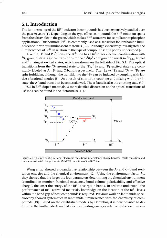
48 The Bi3+ 6s and 6p electron binding energies
5.1. IntroductionThe luminescence of the Bi3+ activator in compounds has been extensively studied overthe past 50 years [1]. Depending on the type of host compound, the Bi3+ emission spansfrom the ultraviolet to the green, which makes Bi3+ attractive for scintillator or phosphorapplications. Furthermore, Bi3+ is commonly used as a sensitizer for lanthanide lumi-nescence in various luminescent materials [2–6]. Although extensively investigated, theluminescence of Bi3+ in relation to the type of compound is still poorly understood [7].
Like the Tl+ and Pb2+ ions, the Bi3+ ion has a 6s2 outer electron configuration with1S0 ground state. Optical transitions to the 6s16p1 configuration result in 3P0,1,2 tripletand 1P1 singlet excited states, which are shown on the left side of Fig. 5.1. The opticaltransitions from the 1S0 ground state to the 3P1, 3P2 and 1P1 excited states are com-monly labeled as A-, B- and C-band, respectively. The 1S0 → 3P0 and 1S0 → 3P2 arespin-forbidden, although the transition to the 3P2 can be induced by coupling with lat-tice vibrational modes [8]. As a result of spin-orbit coupling and mixing with the 1P1
state, the A-band transition becomes allowed. The A-band is also the emitting state (3P1
→ 1S0) in Bi3+ doped materials. A more detailed discussion on the optical transitions of6s2 ions can be found in the literature [9–11].
I V C T
B i 3 +
3 P 13 P 0
B
B i 2 +
C
M M C T
1 S 0B i 3 +
1 P 13 P 2
1 S 0
V a l e n c e b a n d
A
1 S 0
3 P 1
B i 3 +
C o n d u c t i o n b a n d
Figure 5.1: The interconfigurational electronic transitions, intervalence charge transfer (IVCT) transition andthe metal-to-metal charge transfer (MMCT) transition of the Bi3+ ion.
Wang et al. showed a quantitative relationship between the A- and C- band exci-tation energies and the chemical environment [12]. Using the environment factor he ,they showed that the larger the four parameters determining the chemical environment(coordination number, fractional covalence, bond volume polarizability and effectivecharge), the lower the energy of the Bi3+ absorption bands. In order to understand theperformance of Bi3+ activated materials, knowledge on the location of the Bi3+ levelswithin the band gap of host compounds is required. Previous work on lanthanide spec-troscopy showed systematics in lanthanide luminescence with the chemistry of com-pounds [13]. Based on the established models by Dorenbos, it is now possible to de-termine the lanthanide 4f and 5d electron binding energies relative to the vacuum en-
5.2. Methodology 49
ergy [14]. Combined with the binding energy at the conduction band bottom and va-lence band top, it is not only possible to understand but also to predict the propertiesof lanthanide activated materials. In 2014 these models were applied to determine thevacuum referred binding energies of the 3d electron in transition metal ions [15]. In thischapter, based on the same models, the binding energies of the 6s and 6p electrons ofBi3+ are determined in 44 different compounds.
An important parameter required to determine the binding energy of an electron isa charge transfer transition. In the case of the lanthanides, the charge transfer of a va-lence band electron to a trivalent lanthanide can be used to locate the ground state ofthe divalent lanthanide relative to the top of the valence band [16]. Additionally, in forexample Pr3+ or Tb3+ doped phosphors, an electron transfer from the 4f ground stateto the conduction band is possible, which can be used to locate the ground state of thetrivalent lanthanide relative to the bottom of the conduction band. These charge trans-fer transitions are called metal-to-metal charge transfer (MMCT) transitions [17]. Alsoin the case of Bi3+ a MMCT transition of an electron from Bi3+ to a host cation (Mn+)exists, i.e. Bi3+/Mn+ → Bi4+/M(n−1)+, which is shown on the right side of Fig. 5.1 [18, 19].Recently, Boutinaud et al. reported on the systematics of the Bi3+ MMCT transition ind0 and d10 transition metal oxides [20, 21]. Another possibility proposed by Srivastava etal. is that Bi3+ ions enter the host lattice in the form of pairs or clusters [22, 23]. Con-sidering a pair of neighboring Bi3+ ions, a charge transfer of an electron from one Bi3+ion to its neighbor is possible, forming Bi2+ and Bi4+ ions. To distinguish between thecharge transfer of an electron from a Bi3+ ion to either the conduction band or to a neigh-boring Bi3+ we introduce the term intervalence charge transfer (IVCT). Here we refer toIVCT as a charge transfer between two neighboring Bi3+ ions, as indicated by the dashedarrows in Fig. 5.1. The IVCT is only possible when the ground state of Bi2+ is locatedbelow the first excited state of Bi3+. In chapter 3 we suggested that the ground state ofBi2+ is indeed located below the 3P1 excited state of Bi3+ in Li2BaP2O7. Furthermore, wesuggested that the intervalence charge transfer transition between neighboring bismuthions can be responsible for the complete quenching of the Bi3+ A-band luminescence.
In most of the Bi3+-doped compounds an additional emission band is observed atenergies lower than the A-band. In the literature this emission band is commonly labeledas VIS-band, since the emission energy is usually in the visible part of the spectrum,whereas the A-band is usually located in the ultraviolet. The origin of the lower energyemission band remains controversial, however, emission from Bi3+-pairs or from thecharge transfer state have been suggested [20, 22]. Dedicated experiments are requiredto determine the binding energy of an electron in the ground state of the Bi2+ ion incompounds in order to make a thorough evaluation and distinction of the Bi3+ MMCTand IVCT transition energies.
5.2. MethodologySpectroscopic data on the electronic transitions of Bi3+ in 117 different compounds havebeen collected from the archival literature and have been compiled in Table 5.1. The firstcolumn lists the 7-digit compound identification number that characterizes the type ofcompound and reflects an increasing value for the redshift of the 4f-5d transition of lan-
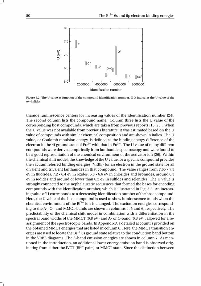
50 The Bi3+ 6s and 6p electron binding energies
2 0 0 0 0 0 0 4 0 0 0 0 0 0 6 0 0 0 0 0 0 8 0 0 0 0 0 06 . 0
6 . 5
7 . 0
7 . 5
8 . 0
O 2 -
O - X
U (eV
)
I d e n t i f i c a t i o n n u m b e r
F -
C l -B r -
I - S 2 - S e 2 -
Figure 5.2: The U value as function of the compound identification number. O-X indicates the U value of theoxyhalides.
thanide luminescence centers for increasing values of the identification number [24].The second column lists the compound name. Column three lists the U value of thecorresponding host compounds, which are taken from previous reports [15, 25]. Whenthe U value was not available from previous literature, it was estimated based on the Uvalue of compounds with similar chemical composition and are shown in italics. The Uvalue, or Coulomb repulsion energy, is defined as the binding energy difference of theelectron in the 4f ground state of Eu2+ with that in Eu3+. The U value of many differentcompounds were derived empirically from lanthanide spectroscopy and were found tobe a good representation of the chemical environment of the activator ion [26]. Withinthe chemical shift model, the knowledge of the U value for a specific compound providesthe vacuum referred binding energies (VRBE) for an electron in the ground state for alldivalent and trivalent lanthanides in that compound. The value ranges from 7.65 - 7.3eV in fluorides, 7.2 - 6.4 eV in oxides, 6.8 - 6.6 eV in chlorides and bromides, around 6.3eV in iodides and around or lower than 6.2 eV in sulfides and selenides. The U value isstrongly connected to the nephelauxetic sequences that formed the bases for encodingcompounds with the identification number, which is illustrated in Fig. 5.2. An increas-ing value of U corresponds to a decreasing identification number of the host compound.Here, the U value of the host compound is used to show luminescence trends when thechemical environment of the Bi3+ ion is changed. The excitation energies correspond-ing to the A-, C-, and MMCT-bands are shown in columns 4, 5 and 6, respectively. Thepredictability of the chemical shift model in combination with a differentiation in thespectral band widths of the MMCT (0.8 eV) and A- or C-band (0.3 eV), allowed for a re-assignment of the spectroscopic bands. In Appendix A a detailed account is provided onthe obtained MMCT energies that are listed in column 6. Here, the MMCT transition en-ergies are used to locate the Bi3+ 6s ground state relative to the conduction band bottomin the VRBE diagrams. The A-band emission energies are shown in column 7. As men-tioned in the introduction, an additional lower energy emission band is observed orig-inating from either the IVCT (Bi3+ pairs) or MMCT state. Since the distinction between
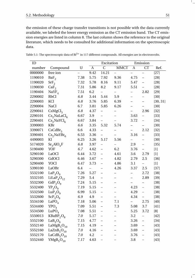
5.2. Methodology 51
the emission of these charge transfer transitions is not possible with the data currentlyavailable, we labeled the lower energy emission as the CT emission band. The CT emis-sion energies are listed in column 8. The last column shows the reference to the originalliterature, which needs to be consulted for additional information on the spectroscopicdata.
Table 5.1: The spectroscopic data of Bi3+ in 117 different compounds. All energies are in electronvolts.
ID Excitation Emissionnumber Compound U A C MMCT A CT Ref.
0000000 free ion – 9.42 14.21 – – – [27]1190010 BaF2 7.38 5.75 7.92 9.36 4.75 – [28]1190020 SrF2 7.32 5.78 8.16 9.11 5.47 – [28]1190030 CaF2 7.31 5.86 8.2 9.17 5.51 – [28]1190404 NaYF4 7.51 6.2 – – – 2.82 [29]2290002 RbCl 6.8 3.44 5.44 5.9 – – [30]2290003 KCl 6.8 3.76 5.85 6.39 – – [30, 31]2290004 NaCl 6.7 3.81 5.85 6.26 – – [30]2290041 CsMgCl3 6.8 4.37 – – – 2.96 [32]2290101 Cs2NaLaCl6 6.67 3.9 – – 3.63 – [33]2290401 Cs2NaYCl6 6.67 3.84 – – 3.72 – [34]3390003 KBr 6.6 3.35 5.32 5.74 – – [30]3390071 CsCdBr3 6.6 4.33 – – – 2.12 [32]3390401 Cs2NaYBr6 6.53 3.36 – – 3.16 – [33]4490003 KI 6.25 3.26 5.17 5.56 – – [30]5174020 Sr3AlO4F 6.8 3.97 – – 2.9 – [35]5190400 YOF 6.7 4.62 – 6.2 3.76 – [1]5290100 LaOCl 6.44 3.72 – 4.61 3.6 2.79 [1]5290300 GdOCl 6.46 3.67 – 4.82 2.79 2.5 [36]5290400 YOCl 6.47 3.73 – 4.86 3.1 – [1]5390100 LaOBr 6.4 – – 4.26 3.37 2.5 [37]5532100 LaP3O9 7.26 5.27 – – – 2.72 [38]5532105 LiLaP4O12 7.29 5.4 – – – 2.89 [39]5532300 GdP3O9 7.24 5.15 – – – – [38]5532400 YP3O9 7.19 5.15 – – 4.23 – [38]5532500 LuP3O9 6.99 5.15 – – 4.29 – [38]5532600 ScP3O9 6.9 4.9 – – 4.34 – [38]5534100 LaPO4 7.18 5.06 – 7.1 – 2.75 [40]5534400 YPO4 7.09 5.51 – 7.3 5.08 3.7 [41]5534500 LuPO4 7.08 5.51 – – 5.25 3.72 [8]5550013 KBaBP2O8 7.0 5.17 – – 3.2 – [42]5552100 LaB3O6 7.15 4.77 – – 3.26 – [34]5552140 LaMgB5O10 7.15 4.19 – – 3.69 – [43]5552160 LaZnB5O10 7.0 4.16 – – 3.69 – [43]5552170 LaCdB5O10 7.0 4.2 – – 3.76 – [43]5552440 YMgB5O10 7.17 4.63 – – 3.8 – [43]
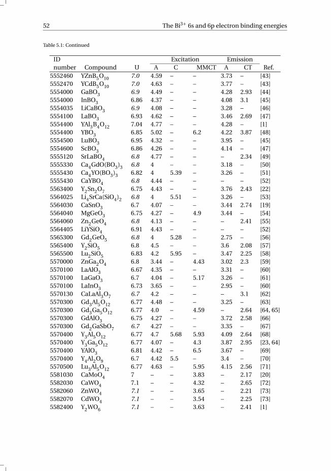
52 The Bi3+ 6s and 6p electron binding energies
Table 5.1: Continued
ID Excitation Emissionnumber Compound U A C MMCT A CT Ref.
5552460 YZnB5O10 7.0 4.59 – – 3.73 – [43]5552470 YCdB5O10 7.0 4.63 – – 3.77 – [43]5554000 GaBO3 6.9 4.49 – – 4.28 2.93 [44]5554000 InBO3 6.86 4.37 – – 4.08 3.1 [45]5554035 LiCaBO3 6.9 4.08 – – 3.28 – [46]5554100 LaBO3 6.93 4.62 – – 3.46 2.69 [47]5554400 YAl3B4O12 7.04 4.77 – – 4.28 – [1]5554400 YBO3 6.85 5.02 – 6.2 4.22 3.87 [48]5554500 LuBO3 6.95 4.32 – – 3.95 – [45]5554600 ScBO3 6.86 4.26 – – 4.14 – [47]5555120 SrLaBO4 6.8 4.77 – – – 2.34 [49]5555330 Ca4GdO(BO3)3 6.8 4 – – 3.18 – [50]5555430 Ca4YO(BO3)3 6.82 4 5.39 – 3.26 – [51]5555430 CaYBO4 6.8 4.44 – – – – [52]5563400 Y2Sn2O7 6.75 4.43 – – 3.76 2.43 [22]5564025 Li4SrCa(SiO4)2 6.8 4 5.51 – 3.26 – [53]5564030 CaSnO3 6.7 4.07 – – 3.44 2.74 [19]5564040 MgGeO3 6.75 4.27 – 4.9 3.44 – [54]5564060 Zn2GeO4 6.8 4.13 – – – 2.41 [55]5564405 LiYSiO4 6.91 4.43 – – – – [52]5565300 Gd2GeO5 6.8 4 5.28 – 2.75 – [56]5565400 Y2SiO5 6.8 4.5 – – 3.6 2.08 [57]5565500 Lu2SiO5 6.83 4.2 5.95 – 3.47 2.25 [58]5570000 ZnGa2O4 6.8 3.44 – 4.43 3.02 2.3 [59]5570100 LaAlO3 6.67 4.35 – – 3.31 – [60]5570100 LaGaO3 6.7 4.04 – 5.17 3.26 – [61]5570100 LaInO3 6.73 3.65 – – 2.95 – [60]5570130 CaLaAl3O7 6.7 4.2 – – – 3.1 [62]5570300 Gd3Al5O12 6.77 4.48 – – 3.25 – [63]5570300 Gd3Ga5O12 6.77 4.0 – 4.59 – 2.64 [64, 65]5570300 GdAlO3 6.75 4.27 – – 3.72 2.58 [66]5570300 Gd2GaSbO7 6.7 4.27 – – 3.35 – [67]5570400 Y3Al5O12 6.77 4.7 5.68 5.93 4.09 2.64 [68]5570400 Y3Ga5O12 6.77 4.07 – 4.3 3.87 2.95 [23, 64]5570400 YAlO3 6.81 4.42 – 6.5 3.67 – [69]5570400 Y4Al2O9 6.7 4.42 5.5 – 3.4 – [70]5570500 Lu3Al5O12 6.77 4.63 – 5.95 4.15 2.56 [71]5581030 CaMoO4 7 – – 3.83 – 2.17 [20]5582030 CaWO4 7.1 – – 4.32 – 2.65 [72]5582060 ZnWO4 7.1 – – 3.65 – 2.21 [73]5582070 CdWO4 7.1 – – 3.54 – 2.25 [73]5582400 Y2WO6 7.1 – – 3.63 – 2.41 [1]
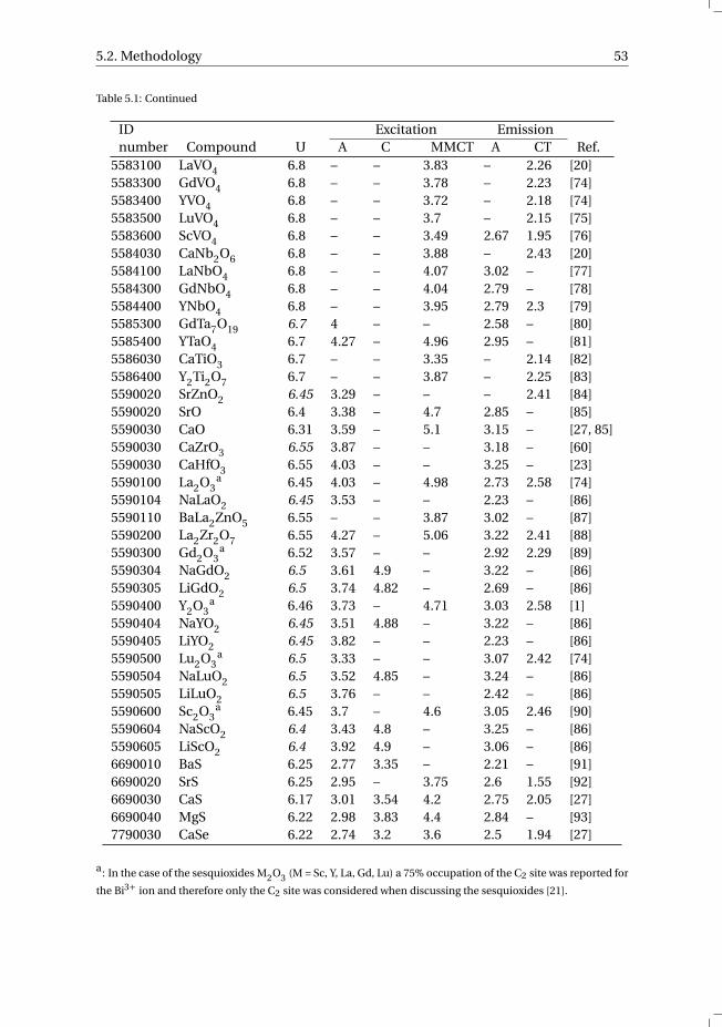
5.2. Methodology 53
Table 5.1: Continued
ID Excitation Emissionnumber Compound U A C MMCT A CT Ref.
5583100 LaVO4 6.8 – – 3.83 – 2.26 [20]5583300 GdVO4 6.8 – – 3.78 – 2.23 [74]5583400 YVO4 6.8 – – 3.72 – 2.18 [74]5583500 LuVO4 6.8 – – 3.7 – 2.15 [75]5583600 ScVO4 6.8 – – 3.49 2.67 1.95 [76]5584030 CaNb2O6 6.8 – – 3.88 – 2.43 [20]5584100 LaNbO4 6.8 – – 4.07 3.02 – [77]5584300 GdNbO4 6.8 – – 4.04 2.79 – [78]5584400 YNbO4 6.8 – – 3.95 2.79 2.3 [79]5585300 GdTa7O19 6.7 4 – – 2.58 – [80]5585400 YTaO4 6.7 4.27 – 4.96 2.95 – [81]5586030 CaTiO3 6.7 – – 3.35 – 2.14 [82]5586400 Y2Ti2O7 6.7 – – 3.87 – 2.25 [83]5590020 SrZnO2 6.45 3.29 – – – 2.41 [84]5590020 SrO 6.4 3.38 – 4.7 2.85 – [85]5590030 CaO 6.31 3.59 – 5.1 3.15 – [27, 85]5590030 CaZrO3 6.55 3.87 – – 3.18 – [60]5590030 CaHfO3 6.55 4.03 – – 3.25 – [23]5590100 La2O3
a 6.45 4.03 – 4.98 2.73 2.58 [74]5590104 NaLaO2 6.45 3.53 – – 2.23 – [86]5590110 BaLa2ZnO5 6.55 – – 3.87 3.02 – [87]5590200 La2Zr2O7 6.55 4.27 – 5.06 3.22 2.41 [88]5590300 Gd2O3
a 6.52 3.57 – – 2.92 2.29 [89]5590304 NaGdO2 6.5 3.61 4.9 – 3.22 – [86]5590305 LiGdO2 6.5 3.74 4.82 – 2.69 – [86]5590400 Y2O3
a 6.46 3.73 – 4.71 3.03 2.58 [1]5590404 NaYO2 6.45 3.51 4.88 – 3.22 – [86]5590405 LiYO2 6.45 3.82 – – 2.23 – [86]5590500 Lu2O3
a 6.5 3.33 – – 3.07 2.42 [74]5590504 NaLuO2 6.5 3.52 4.85 – 3.24 – [86]5590505 LiLuO2 6.5 3.76 – – 2.42 – [86]5590600 Sc2O3
a 6.45 3.7 – 4.6 3.05 2.46 [90]5590604 NaScO2 6.4 3.43 4.8 – 3.25 – [86]5590605 LiScO2 6.4 3.92 4.9 – 3.06 – [86]6690010 BaS 6.25 2.77 3.35 – 2.21 – [91]6690020 SrS 6.25 2.95 – 3.75 2.6 1.55 [92]6690030 CaS 6.17 3.01 3.54 4.2 2.75 2.05 [27]6690040 MgS 6.22 2.98 3.83 4.4 2.84 – [93]7790030 CaSe 6.22 2.74 3.2 3.6 2.5 1.94 [27]
a: In the case of the sesquioxides M2O3 (M = Sc, Y, La, Gd, Lu) a 75% occupation of the C2 site was reported for
the Bi3+ ion and therefore only the C2 site was considered when discussing the sesquioxides [21].
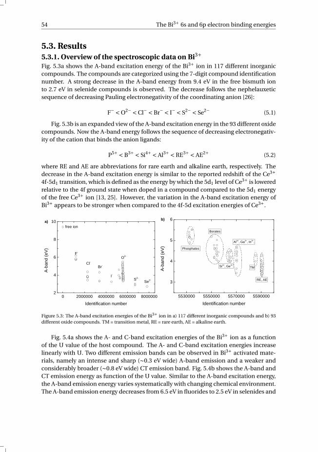
54 The Bi3+ 6s and 6p electron binding energies
5.3. Results5.3.1. Overview of the spectroscopic data on Bi3+Fig. 5.3a shows the A-band excitation energy of the Bi3+ ion in 117 different inorganiccompounds. The compounds are categorized using the 7-digit compound identificationnumber. A strong decrease in the A-band energy from 9.4 eV in the free bismuth ionto 2.7 eV in selenide compounds is observed. The decrease follows the nephelauxeticsequence of decreasing Pauling electronegativity of the coordinating anion [26]:
F− < O2− < Cl− < Br− < I− < S2− < Se2− (5.1)
Fig. 5.3b is an expanded view of the A-band excitation energy in the 93 different oxidecompounds. Now the A-band energy follows the sequence of decreasing electronegativ-ity of the cation that binds the anion ligands:
P5+ < B3+ < Si4+ < Al3+ < RE3+ < AE2+ (5.2)
where RE and AE are abbreviations for rare earth and alkaline earth, respectively. Thedecrease in the A-band excitation energy is similar to the reported redshift of the Ce3+4f-5d1 transition, which is defined as the energy by which the 5d1 level of Ce3+ is loweredrelative to the 4f ground state when doped in a compound compared to the 5d1 energyof the free Ce3+ ion [13, 25]. However, the variation in the A-band excitation energy ofBi3+ appears to be stronger when compared to the 4f-5d excitation energies of Ce3+.
0 2 0 0 0 0 0 0 4 0 0 0 0 0 0 6 0 0 0 0 0 0 8 0 0 0 0 0 02
4
6
8
1 0a )
A-ban
d (eV
)
I d e n t i f i c a t i o n n u m b e r
f r e e i o n
F -
C l - B r -
I -
O 2 -
S 2 -S e 2 -
5 5 3 0 0 0 0 5 5 5 0 0 0 0 5 5 7 0 0 0 0 5 5 9 0 0 0 0
3
4
5
6b )
A-ban
d (eV
)
I d e n t i f i c a t i o n n u m b e r
P h o s p h a t e s
B o r a t e s
S i 4 + , G e 4 +
A l 3 + , G a 3 + , I n 3 + ,
R E , A E
T M
Figure 5.3: The A-band excitation energies of the Bi3+ ion in a) 117 different inorganic compounds and b) 93different oxide compounds. TM = transition metal, RE = rare earth, AE = alkaline earth.
Fig. 5.4a shows the A- and C-band excitation energies of the Bi3+ ion as a functionof the U value of the host compound. The A- and C-band excitation energies increaselinearly with U. Two different emission bands can be observed in Bi3+ activated mate-rials, namely an intense and sharp (∼0.3 eV wide) A-band emission and a weaker andconsiderably broader (∼0.8 eV wide) CT emission band. Fig. 5.4b shows the A-band andCT emission energy as function of the U value. Similar to the A-band excitation energy,the A-band emission energy varies systematically with changing chemical environment.The A-band emission energy decreases from 6.5 eV in fluorides to 2.5 eV in selenides and
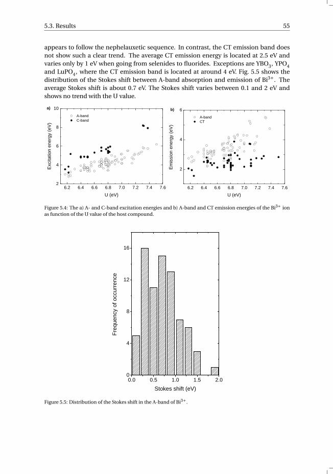
5.3. Results 55
appears to follow the nephelauxetic sequence. In contrast, the CT emission band doesnot show such a clear trend. The average CT emission energy is located at 2.5 eV andvaries only by 1 eV when going from selenides to fluorides. Exceptions are YBO3, YPO4and LuPO4, where the CT emission band is located at around 4 eV. Fig. 5.5 shows thedistribution of the Stokes shift between A-band absorption and emission of Bi3+. Theaverage Stokes shift is about 0.7 eV. The Stokes shift varies between 0.1 and 2 eV andshows no trend with the U value.
6 . 2 6 . 4 6 . 6 6 . 8 7 . 0 7 . 2 7 . 4 7 . 62
4
6
8
1 0a ) A - b a n d C - b a n d
Excita
tion e
nergy
(eV)
U ( e V )6 . 2 6 . 4 6 . 6 6 . 8 7 . 0 7 . 2 7 . 4 7 . 6
2
4
6b )
Emiss
ion en
ergy (
eV)
A - b a n d C T
U ( e V )
Figure 5.4: The a) A- and C-band excitation energies and b) A-band and CT emission energies of the Bi3+ ionas function of the U value of the host compound.
0 . 0 0 . 5 1 . 0 1 . 5 2 . 00
4
8
1 2
1 6
Frequ
ency
of oc
curre
nce
S t o k e s s h i f t ( e V )Figure 5.5: Distribution of the Stokes shift in the A-band of Bi3+.
56 The Bi3+ 6s and 6p electron binding energies
5.3.2. The vacuum referred binding energies in the 6s and 6p electronicstates of Bi3+
Based on the available lanthanide spectroscopy combined with the chemical shift model,it is possible to determine the vacuum referred electron binding energy at the top of thevalence band and the bottom of the conduction band in compounds. The energy of anelectron at rest in the vacuum is here defined as energy zero. For 44 of the compounds inTable 5.1 this information was already gathered in Refs. [15, 26, 94–96]. Using the MMCTenergy, one may determine the electron binding energy in the 6s2 ground state with re-spect to that at the bottom of the conduction band as shown in Fig. 5.1. The A-bandexcitation energy was then used to determine the VRBE of the electron in the 3P1 excitedstate. The vacuum referred binding energies of the electron in the 6s and 6p levels of theBi3+ ion in 44 different compounds are shown in Fig. 5.7. EX is the VRBE of the electronin the host exciton state. The binding energies in the 6s ground state tend to decreasewith increasing U value and are always located above the valence band top. The bind-ing energy in the 6p level also indicates a general decrease with increasing U value butappears to follow the location of the host conduction band.
6 . 2 6 . 4 6 . 6 6 . 8 7 . 0 7 . 2 7 . 4- 1 2
- 1 0
- 8
- 6
- 4
- 2
0
6 . 2 6 . 4 6 . 6 6 . 8 7 . 0 7 . 2 7 . 4- 1 2
- 1 0
- 8
- 6
- 4
- 2
0
U ( e V )
U ( e V )
Y P O 4
Y P O 4
1 S 0
3 P 1
U ( e V )
VRBE
(eV)
Figure 5.6: The vacuum referred electron binding energy in the 1S0 ground state and 3P1 excited state of theBi3+ ion as function of the U value.
Fig. 5.6 shows the VRBE in the 1S0 ground and 3P1 excited state of the Bi3+ ion asfunction of the U value of the host compound. The 1S0 ground state VRBE decreasesfrom -5 eV to -10 eV with increasing U value, while the 3P1 excited state VRBE decreasesless strongly from -2 to -4 eV. The difference between both sets of data are then the A-band energies shown in Fig. 5.3. Both the 6s and 6p data points in Fig. 5.6 spread by ±1eV around the drawn lines.
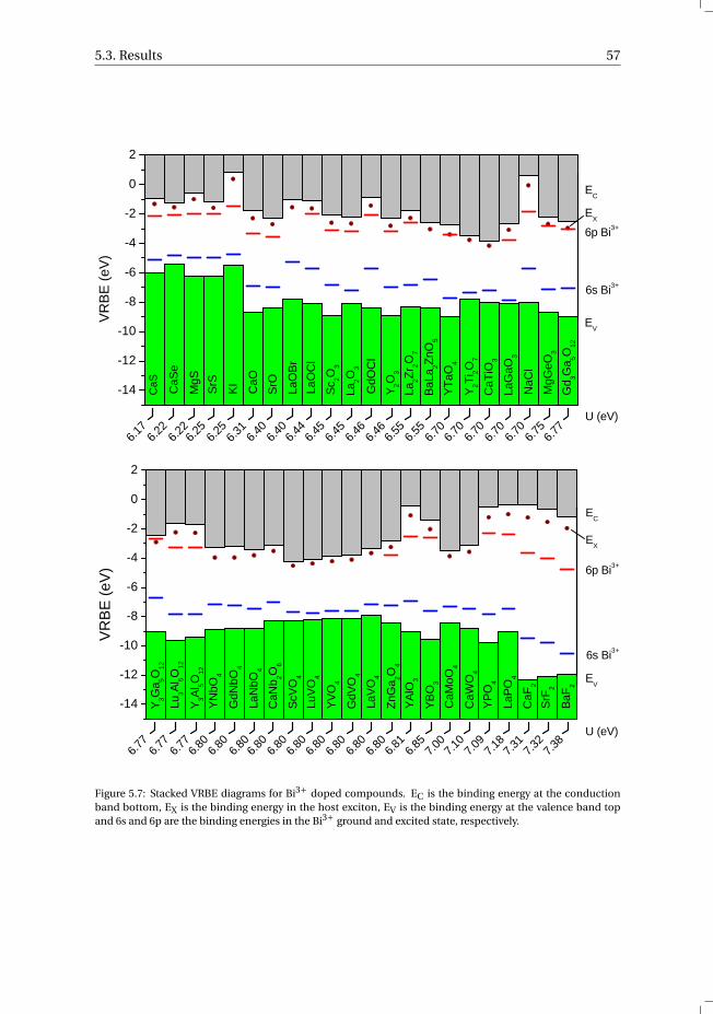
5.3. Results 57
- 1 4- 1 2- 1 0
- 8- 6- 4- 202
E V
VRBE
(eV)
6 . 3 1
KISrSMgS
CaSe
CaS
Sc2O
3
LaOC
lLa
OBr
CaO
SrO La2O
3Gd
OCl
Y 2O3
La2Zr
2O7
BaLa
2ZnO 5
YTaO
4
CaTiO
3
Y 2Ti2O
7
NaCl
LaGa
O 3
6 . 2 56 . 2 26 . 1 7 6 . 2 56 . 2 2 6 . 4 56 . 4 0 6 . 4 46 . 4 0 6 . 4 5 6 . 4 6 6 . 4 6 6 . 7 06 . 5 56 . 5 5 6 . 7 06 . 7 0 6 . 7 06 . 7 0
6 s B i 3 +
6 p B i 3 +E X
U ( e V )
E C
MgGe
O 3
6 . 7 5 6 . 7 7
Gd3G
a 5O12
- 1 4- 1 2- 1 0
- 8- 6- 4- 202
E V
6 . 8 0
GdNb
O 4
YNbO
4
Y 3Al5O
12
Lu3Al
5O12
VRBE
(eV)
Y 3Ga 5O
12
6 s B i 3 +
6 p B i 3 +
E X
U ( e V )
E C
YVO 4
LuVO
4
ScVO
4
LaNb
O 4Ca
Nb2O
6
GdVO
4La
VO4
ZnGa
2O4
YAlO 3
YBO 3
CaMo
O 4Ca
WO4
YPO 4
LaPO
4
BaF 2
SrF2
CaF 2
6 . 8 06 . 7 76 . 7 7 6 . 8 06 . 7 7 6 . 8 06 . 8 0 6 . 8 06 . 8 0 6 . 8 0 6 . 8 0 6 . 8 0 7 . 0 06 . 8 56 . 8 1 7 . 1 87 . 0 97 . 1 0 7 . 3 87 . 3 27 . 3 1
Figure 5.7: Stacked VRBE diagrams for Bi3+ doped compounds. EC is the binding energy at the conductionband bottom, EX is the binding energy in the host exciton, EV is the binding energy at the valence band topand 6s and 6p are the binding energies in the Bi3+ ground and excited state, respectively.
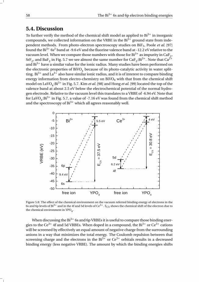
58 The Bi3+ 6s and 6p electron binding energies
5.4. DiscussionTo further verify the method of the chemical shift model as applied to Bi3+ in inorganiccompounds, we collected information on the VRBE in the Bi3+ ground state from inde-pendent methods. From photo-electron spectroscopy studies on BiF3, Poole et al. [97]found the Bi3+ 6s2 band at -9.6 eV and the fluorine valence band at -12.2 eV relative to thevacuum level. When we compare those numbers with those for Bi3+ as impurity in CaF2,SrF2, and BaF2 in Fig. 5.7 we see almost the same number for CaF2:Bi3+. Note that Ca2+and Bi3+ have a similar value for the ionic radius. Many studies have been performed onthe electronic properties of BiVO4 because of its photo-catalytic activity in water split-ting. Bi3+ and La3+ also have similar ionic radius, and it is of interest to compare bindingenergy information from electro-chemistry on BiVO4 with that from the chemical shiftmodel on LaVO4:Bi3+ in Fig. 5.7. Kim et al. [98] and Hong et al. [99] located the top of thevalence band at about 2.5 eV below the electrochemical potential of the normal hydro-gen electrode. Relative to the vacuum level this translates to a VRBE of -6.94 eV. Note thatfor LaVO4:Bi3+ in Fig. 5.7, a value of -7.16 eV was found from the chemical shift methodand the spectroscopy of Bi3+ which all agrees reasonably well.
- 5 0- 4 5- 4 0- 3 5- 3 0- 2 5- 2 0- 1 5- 1 0
- 50
B i 3 +
f r e e i o n Y P O 4
VRBE
(eV)
E CS =
37.5
eV
6 s
6 p
9 . 4 e V
5 . 5 e V
f r e e i o n Y P O 4
E CS =
30.8
eV
4 f
5 d6 . 2 e V
4 e VC e 3 +
Figure 5.8: The effect of the chemical environment on the vacuum referred binding energy of electrons in the6s and 6p levels of Bi3+ and in the 4f and 5d levels of Ce3+. ECS shows the chemical shift of the electron due tothe chemical environment in YPO4.
When discussing the Bi3+ 6s and 6p VRBEs it is useful to compare those binding ener-gies to the Ce3+ 4f and 5d VRBEs. When doped in a compound, the Bi3+ or Ce3+ cationswill be screened by effectively an equal amount of negative charge from the surroundinganions in a way that minimizes the total energy. The Coulomb repulsion between thatscreening charge and the electrons in the Bi3+ or Ce3+ orbitals results in a decreasedbinding energy (less negative VRBE). The amount by which the binding energies shifts
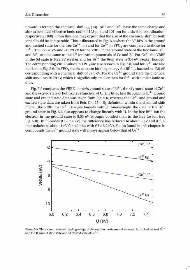
5.4. Discussion 59
upward is termed the chemical shift ECS [14]. Bi3+ and Ce3+ have the same charge andalmost identical effective ionic radii of 103 pm and 101 pm for a six-fold coordination,respectively [100]. From this, one may expect that the size of the chemical shift for bothions should be comparable. This is illustrated in Fig. 5.8 where the VRBEs in the groundand excited state for the free Ce3+ ion and for Ce3+ in YPO4 are compared to those forBi3+. The -36.76 eV and -45.29 eV for the VRBE in the ground state of the free ions Ce3+and Bi3+ are the same as the 4th ionization potentials of Ce and Bi. For Ce3+ the VRBEin the 5d state is 6.22 eV weaker and for Bi3+ the 6s6p state is 9.4 eV weaker bonded.The corresponding VRBE values in YPO4 are also shown in Fig. 5.8, and for Bi3+ are alsomarked in Fig. 5.6. In YPO4 the 6s electron binding energy for Bi3+ is located at -7.8 eV,corresponding with a chemical shift of 37.5 eV. For the Ce3+ ground state the chemicalshift amounts 30.79 eV, which is significantly smaller than for Bi3+ with similar ionic ra-dius.
Fig. 5.9 compares the VRBE in the 6s ground state of Bi3+, the 4f ground state of Ce3+and the excited state of both ions as function of U. The fitted line through the Bi3+ groundstate and excited state data was taken from Fig. 5.6, whereas the Ce3+ and ground andexcited state data are taken from Refs [14, 15]. By definition within the chemical shiftmodel, the VRBE for Ce3+ changes linearly with U. Interestingly, the data of the Bi3+ground state in Fig. 5.6 also appears to change linearly with U. In the free Bi3+ ion theelectron in the ground state is 8.53 eV stronger bonded than in the free Ce ion (seeFig. 5.8). In fluorides (U = 7.4 eV) the difference has reduced to about 3 eV and it fur-ther reduces to about 1 eV for sulfides with (U = 6.2 eV). Yet, as found in this chapter, incompounds the Bi3+ ground state will always appear below that of Ce3+.
6 . 0 6 . 2 6 . 4 6 . 6 6 . 8 7 . 0 7 . 2 7 . 4
- 1 0
- 8
- 6
- 4
- 2
VRBE
(eV)
U ( e V )
C e 3 + 4 f
B i 3 + 6 s
B i 3 + 6 p
C e 3 + 5 d
Figure 5.9: The vacuum referred binding energy of electrons in the 6s ground state and 6p excited state of Bi3+and the 4f ground state state and 5d excited state of Ce3+.
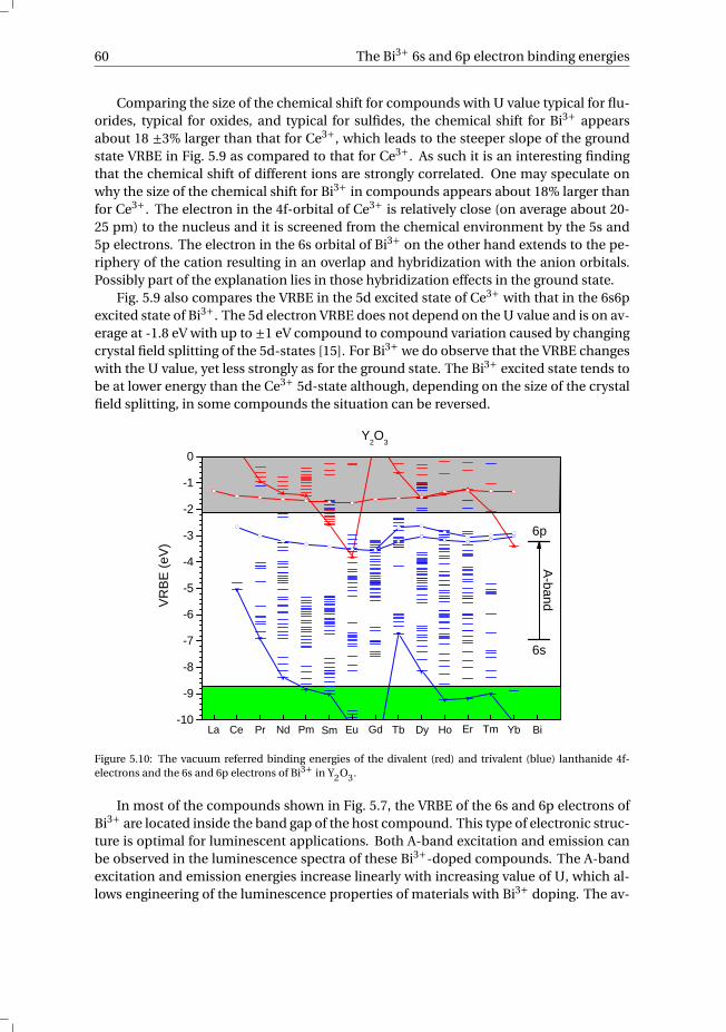
60 The Bi3+ 6s and 6p electron binding energies
Comparing the size of the chemical shift for compounds with U value typical for flu-orides, typical for oxides, and typical for sulfides, the chemical shift for Bi3+ appearsabout 18 ±3% larger than that for Ce3+, which leads to the steeper slope of the groundstate VRBE in Fig. 5.9 as compared to that for Ce3+. As such it is an interesting findingthat the chemical shift of different ions are strongly correlated. One may speculate onwhy the size of the chemical shift for Bi3+ in compounds appears about 18% larger thanfor Ce3+. The electron in the 4f-orbital of Ce3+ is relatively close (on average about 20-25 pm) to the nucleus and it is screened from the chemical environment by the 5s and5p electrons. The electron in the 6s orbital of Bi3+ on the other hand extends to the pe-riphery of the cation resulting in an overlap and hybridization with the anion orbitals.Possibly part of the explanation lies in those hybridization effects in the ground state.
Fig. 5.9 also compares the VRBE in the 5d excited state of Ce3+ with that in the 6s6pexcited state of Bi3+. The 5d electron VRBE does not depend on the U value and is on av-erage at -1.8 eV with up to ±1 eV compound to compound variation caused by changingcrystal field splitting of the 5d-states [15]. For Bi3+ we do observe that the VRBE changeswith the U value, yet less strongly as for the ground state. The Bi3+ excited state tends tobe at lower energy than the Ce3+ 5d-state although, depending on the size of the crystalfield splitting, in some compounds the situation can be reversed.
- 1 0- 9- 8- 7- 6- 5- 4- 3- 2- 10
Y b
Y 2 O 3
G dL a
VRBE
(eV)
C e P r N d P m S m E u T b D y H o E r T m B i
6 s
6 p
A-band
Figure 5.10: The vacuum referred binding energies of the divalent (red) and trivalent (blue) lanthanide 4f-electrons and the 6s and 6p electrons of Bi3+ in Y2O3.
In most of the compounds shown in Fig. 5.7, the VRBE of the 6s and 6p electrons ofBi3+ are located inside the band gap of the host compound. This type of electronic struc-ture is optimal for luminescent applications. Both A-band excitation and emission canbe observed in the luminescence spectra of these Bi3+-doped compounds. The A-bandexcitation and emission energies increase linearly with increasing value of U, which al-lows engineering of the luminescence properties of materials with Bi3+ doping. The av-
5.4. Discussion 61
erage Stokes shift in Fig. 5.5 is at 0.7 eV, while an average Stokes shift of 0.45 eV wasreported for Ce3+. The Stokes shift originates from the relaxation of the host lattice dueto coupling of the excited electron orbital with lattice phonons and can therefore be re-garded as a property of both the lattice and dopant. Apparently, the 6p electron orbitalof Bi3+ has somewhat stronger interaction with the lattice than that of the 5d electronorbital of Ce3+.
Bi3+ is also reported to be a good sensitizer for lanthanide intra-4f luminescence [2–6]. In Fig. 5.10 the VRBE in the 6s and 6p state of Bi3+ and the VRBEs in the 4f and5d of the di- and trivalent lanthanides in Y2O3 are shown as an example. The Bi3+ A-band excitation and emission energy spectrally matches with the 4f transitions of thelanthanides. Furthermore, the VRBE of the Bi3+ 6p level is located above the VRBE ofthe Eu2+ 4f level, indicating that an electron transfer from the excited state of Bi3+ toEu3+ is possible. In such case, both radiative and electron transfer from Bi3+ to Eu3+can be used as sensitizing mechanism for Eu3+ luminescence. Only for transition metalbased compounds in which the conduction band is located at or below -3 eV, the 6pexcited state of Bi3+ is located inside the conduction band. This is for example the casein Bi3+ activated YVO4 shown in Fig. 5.7. Since all Bi3+ interconfigurational transitionsare located inside the conduction band, no A-band luminescence occurs. This is similarto the situation when the lowest 5d level of Ce3+ is located inside the conduction band.Upon excitation in the 5d state, the electron auto-ionizes and emission is not possible.Instead of A-band emission, in the case of Bi3+, excitation and emission of the MMCTtransition can be observed.
The VRBE diagrams in Fig. 5.7 show that the Bi3+ 6s ground state is always locatedabove the valence band. There appears to be a correlation of the electron binding en-ergies in the 6s state and the valence band top. The chemical shift increases when theelectronegativity of the anion decreases. As a result of this weaker bonding, the VRBEof both the anion electrons and Bi3+ become less negative. Since the Bi3+ ground stateis always located above the valence band, Bi3+ can act as a trap for holes created in thevalence band when exposed to ionizing radiation. Depending on the type of the hostcompound, Bi3+ can act as a deep hole trapping level, like in CaF2 or NaCl (2.82 and2.33 eV, respectively), or a shallow trap, like in the vanadates (0.6 ±0.15 eV). Ce3+ canonly trap an electron to become Ce2+ when the CB bottom is above -1 eV, which is usu-ally not the case. Whether Bi3+ can trap an electron to become Bi2+ depends on theVRBE in the lowest 6s26p level of Bi2+ compared to that at the CB bottom. In the past 20years, Bi2+ luminescence has been reported in wide band gap compounds such as sul-fates, borates and phosphates [101–103], which is only possible when both the excitedand ground state of Bi2+ are located below the bottom of the conduction band, and forthose compounds Bi3+ would also act as an electron trap. Unfortunately, no informationon a charge transfer transition between the host VB and Bi3+ was reported that could beused as a method to locate the Bi2+ ground state within the band gap. The fact that Ce3+5d-4f emission has never been reported in Bi3+ based compounds suggests that, uponexcitation to the 5d-level, emission is fully quenched by electron transfer to the Bi. Inother words it suggests that the VRBE in the Bi2+ ground state is below the VRBE in theCe3+ 5d excited state. In chapter 6 the VRBE in the Bi2+ levels and its implications for theluminescence properties will be presented.
62 The Bi3+ 6s and 6p electron binding energies
5.5. Summary and conclusionsSpectroscopic data on the metal-to-metal charge transfer and interconfigurational A-and C-band transitions of the Bi3+ ion in 117 different compounds were collected fromthe archival literature. Using the MMCT and A-band transition energies it was possibleto determine the vacuum referred binding energy of the 6s and 6p electron in 44 differentcompounds. The obtained VRBE in the Bi3+ ground state are consistent with the VRBEobtained independently from photo-electron spectroscopy and electrochemical studieson BiF3 and BiVO4. The VRBE of the electron in the 6s and 6p levels were found to linearlydecrease with the U value and follow the nephelauxetic sequence. The VRBE in the Bi3+6s ground state is always located above the valence band and below the VRBE of the Ce3+4f ground state. The chemical shift for Bi3+ was found 18 ±3% larger than that for Ce3+.A larger hybridization of the Bi3+ 6s orbital with the anion orbitals compared to that ofthe shielded Ce3+ 4f electrons was suggested as a possible origin.
5.6. Appendix A. The metal-to-metal charge transfer ener-gies of Bi3+
Below an account is given on how the metal-to-metal charge transfer energies in Ta-ble 5.1 were obtained. The data is extracted from excitation or absorption spectra re-ported in the original literature. Since the assignment of the Bi3+ interconfigurationalelectronic transitions (A-, B-, and C-band) are rather straightforward, we limit ourselvesto discussing only the MMCT transitions and refer to the original literature for additionalinformation on the other Bi3+-related transitions.Alkaline earth fluorides. Oboth et al. reported the optical absorption and emission ofBi3+-doped CaF2, SrF2 and BaF2 [28]. An approximately 0.5 eV broad absorption bandat 9.17 eV in the absorption spectrum of CaF2 was observed, which they interpreted asthe MMCT band. Similar assignments for the MMCT-band in Bi3+-doped SrF2 and BaF2were given.Alkali halides. Nistor et al. observed an additional band on the high-energy side of theC-band in the optical absorption spectrum of KCl:Bi3+ [31]. Due to the very pronouncedtemperature dependence this band was attributed to a charge transition. We interpretedthis charge transfer transition as the MMCT transition. Radhakrishna reported on theoptical absorption of the Bi3+-doped alkali halides NaCl, KCl, RbCl, KBr and KI [30]. Theyalso observed an additional band on the high-energy side of the C-band, which was la-beled as C3. However, based on the report of Nistor, we propose that this C3 band in theabsorption spectra corresponds to the MMCT transition.Oxyhalides. Blasse and Bril reported two absorption bands for the oxyhalides YOF, LaOCland YOCl [1]. However, only excitation in the higher energy excitation band resulted inemission. Probably the emission under excitation in the lower energy A-band is com-pletely quenched. Similar observations were made in the oxychlorides by Jacquier andby Wolfert and Blasse [36, 104]. We propose that the high-energy excitation is the MMCTtransition. Wolfert and Blasse observed an excitation band at 4.3 eV in Bi3+-doped LaOBr,which they assigned to a charge transfer from the valence band to the Bi3+ ion [37]. How-ever, we propose that this charge transfer transition is in fact the MMCT transition.Phosphates. Cavalli et al. observed a broad excitation band in the range of 6.53 - 8.27 eV
5.6. Appendix A. The metal-to-metal charge transfer energies of Bi3+ 63
in Bi3+-doped YPO4, which they assigned to the C-band [41]. However, this excitationappears to consist of two bands, namely the C- and MMCT-bands. We estimated theMMCT transition at the low energy side of the broad excitation band at approximately7.3 eV. In the excitation spectrum of Bi3+-doped LaPO4 reported by Moncorgé et al. anexcitation band is visible at 7.1 eV, overlapping on the low energy side of the host excitonband at 7.75 eV [40]. They did not assign this excitation band to an optical transition,however, we propose that this excitation is the MMCT transition, in-line with the 7.3 eVMMCT transition of YPO4:Bi3+. Wang et al. observed a broad excitation band between6.2 and 6.9 eV in LaPO4:Bi3+, which they assigned to the C-band. A sharp excitation peakat 10.5 eV was assigned to a CT transition, which would mean that the Bi3+ related chargetransfer transition is larger than the 8.64 eV band gap of LaPO4. Considering the broadshape of the 6.2-6.9 eV band, we propose that this excitation is due to the MMCT.
Borates. Chen et al. reported two emission bands at 4.22 and 3.87 eV in Bi3+-dopedYBO3, originating from two different sites [48]. However, we propose that these are fromisolated Bi3+ centers and emission from the charge transfer state, in agreement with theassignment of the emission bands in LaBO3:Bi3+ by Wolfert et al. [47]. Furthermore, A-band excitation and emission was observed, originating from only one site in YBO3:Bi3+reported by Zhang et al. [105]. The broad shoulder on the the low energy side of the C-band, centered at 6.2 eV in the excitation spectrum reported by Chen et al., could thenbe assigned to the MMCT transition.
Germanates. Katayama et al. reported a broad MMCT transition at 4.9 eV in Bi3+-dopedMgGeO3 [54].
Aluminates. Krasnikov et al. reported a broad excitation band located at E > 6 eV inYAlO3, which they suggested to be from the C-band transition [69]. However, we pro-pose that this band is from the MMCT transition and estimated the center of this bandat approximately 6.5 eV. Zorenko et al. reported charge transfer transitions in Bi3+-dopedY3Al5O12 at 5.25, 5.93 and 6.85 eV, of which they propose that the 5.93 eV transition origi-nates from the Bi3+ → Bi4+ + e− charge transfer transition [68]. The band excitation bandat 5.95 eV observed in Bi3+-doped Lu3Al5O12, originally assigned to the C-band by Babinet al., we also propose to be the MMCT transition [71].
Gallates. Jacquier et al. observed an approximately 0.8 eV wide excitation band at 5.17eV in the excitation spectrum of LaGaO3:Bi3+ [61]. Srivastava also observed a rising edgeof an excitation band at approximately 4.9 eV, but due to the limitations of their setupthey were not able to determine the center of this band [106]. According to Boutin-aud, this energy would match with the energy expected for the MMCT transition [21].Zhuang observed an excitation band at 4.43 eV in ZnGa2O4:Bi3+, which they attributedto a transition of exciton-like origin (Bi4+ + e−) [59]. However, we propose that this isthe MMCT transition. Setlur and Srivastava showed an excitation band at 4.36 eV forBi3+-doped Y3Ga5O12 [23]. Ilmer et al. reported two bands at 4.43 and 4.07 eV for Bi3+-doped Y3Ga5O12 [64]. They mentioned that the 3P1 level is probably very close to theconduction band and that the highest excitation band can be considered as an impuritybound exciton in which the hole resides on the Bi3+ ion and the electron is inside theconduction band. We therefore assigned the 4.43 eV excitation to the MMCT transition.Ilmer also observed two excitation bands at 4.59 and 4.0 eV in Gd3Ga5O12, with identicalassignments as in Y3Ga5O12.
64 The Bi3+ 6s and 6p electron binding energies
Transition metal compounds. Compounds containing transition metal cations gener-ally have a conduction band located at or below -3 eV relative to the vacuum level. Inthose compounds it is to be expected that the Bi3+ 3P1 excited state is located inside theconduction band of the host compound. The only Bi3+ related excitation band in thesetype of compounds that is expected to be observed is the MMCT transition. The excep-tion are the tantalates, which have a conduction band at energies slightly higher than-3 eV, in which the A-band can also be observed. Boutinaud and Cavalli systematicallyinvestigated the MMCT transition of Bi3+ in a variety of closed-shell transition metal ox-ides [20]. In most cases the MMCT transition is observed as a shoulder on the low energyside of the host exciton band. With this knowledge, we have extracted additional MMCTtransitions from the literature on Bi3+-doped transition metal oxides (see references inTable 5.1).
Zirconates. Srivastava and Beers reported two excitation bands in Bi3+-doped La2Zr2O7[88]. The low-energy excitation band at 4.27 eV was assigned to the A-band, whereasthe high-energy excitation band at 5.06 eV was tentatively assigned to the absorptioninto the excitonic state. However, we know the host lattice exciton energy is located ataround 6 eV. Since the MMCT is also exciton-like, we propose that the 5.06 eV excitationband is due to the MMCT transition.
Simple oxides. Ellervee reported a 0.5 eV wide excitation band centered at 5.1 eV and4.7 eV in the excitation spectra of Bi3+-doped CaO and SrO, respectively [85]. Yamashitaand Asano reported this excitation band at 5.28 eV in CaO and van der Steen and Dijcksat approximately 4.84 and 4.71 eV for CaO and SrO, respectively [27, 107]. Similar tothe assignment of the MMCT transition in the sulfides and selenides, we propose thatthese excitation bands correspond to the MMCT transitions. We have taken the valuesreported by Ellervee for the MMCT transition listed in Table 5.1 of this chapter. Boulonreported on the luminescence of Bi3+ in Ln2O3 with Ln = Sc, Lu, Y, Gd and La [74]. Inthe excitation spectra of these rare-earth oxides doped with Bi3+, a high-energy band at4.6-5.0 eV was observed depending on the type of rare-earth. Blasse also reported a highenergy excitation band at 4.71 eV for Y2O3:Bi3+ and Bordun observed these excitationbands in Bi3+ Y2O3 and Sc2O3 ceramics [1, 90]. Although the original literature assignsthese bands to the C-band, we agree with the assignment of Boutinaud, whom suggestedthat these excitation bands should be assigned to the MMCT transition [21]. A chargetransfer transition was also suggested by van de Craats and Blasse to account for theluminescence quenching in Y2O3:Bi3+ [108].
Other oxides. Chang reported a 0.5 eV wide excitation band centered at 3.17 eV, whichwas concentration dependent, becoming broader and intenser with increasing Bi3+ con-centration in BaLa2ZnO5 [87]. This excitation band was assigned to the A-band, however,we propose that this should be assigned to the MMCT transition especially since the ob-served decay time was very slow (milliseconds), whereas typically the Bi3+ A-band is inthe order of nanoseconds to microseconds.
Sulfides and selenides. Yamashita and Asano investigated the luminescence of Bi3+ inCa(S : Se) [27]. For CaS:Bi3+ they observed excitation bands at 4.5, 4.2, 3.54 and 3.02eV which were assigned to the D-band, C-band, B-band and A-band, respectively. TheD excitation band was attributed to the paired ion center, however, this should be thehost exciton band. The assigned B-band is as intense as the observed the A-band. Due
References 65
to the forbidden nature of the B-band transition, this is more likely the allowed C-bandtransition. The 4.2 eV excitation band which was assigned to the C-band is then morelikely the MMCT transition, especially regarding the temperature dependence and thefact this excitation band is twice as broad as the A-band. For CaSe:Bi3+ excitation bandswere observed at 3.85, 3.6, 3.2 and 2.74 eV, which were assigned to the D-band, C-band,B-band and A-band, respectively. Again we propose that the D-band to be the excitonband and the broad 3.6 eV excitation band to be the MMCT transition, considering thehigh temperature dependency of the transition. The 3.2 eV excitation assigned to the for-bidden B-band transition is more likely the C-band. Yamashita et al. showed three bandsin the excitation spectrum of SrS:Bi3+ at 4.65, 3.75 and 2.95 eV, which were assigned toexciton, C-band and A-band, respectively [92]. However, due the strong temperature de-pendence of the 3.75 eV excitation band and the fact that this excitation band is ratherbroad (0.5 eV) we suggest that this band should be assigned to the MMCT transition. ForMgS, Asano and Yamashita reported excitation bands at 4.4, 3.83 and 2.98 eV, which theyassigned to the charge transfer transition, the C-band and the A-band, respectively [93].
References[1] G. Blasse and A. Bril, Investigations of Bi3+-activated phosphors, J. Chem. Phys. 48,
217 (1968).
[2] G. Blasse and A. Bril, Study of energy transfer from Sb3+, Bi3+ and Ce3+ to Sm3+,Eu3+, Tb3+, Dy3+, J. Chem. Phys. 47, 1920 (1967).
[3] H. S. Kiliaan and G. Blasse, A study of the sensitizer in the luminescent sys-tems (Y,Gd)2O2SO4:Bi,Tb and Li6(Y,Gd)(BO3)3:S,Tb (S=Ce3+, Pr3+ or Bi3+), Mater.Chem. Phys. 18, 155 (1987).
[4] N.-F. Zhu, Y.-X. Li, and X.-F. Yu, Luminescence spectra of YGG:RE3+, Bi3+ (RE = Euand Tb) and energy transfer from Bi3+ to RE3+, Chin. Phys. Lett. 25, 703 (2008).
[5] M. Back, E. Trave, R. Marin, N. Mazzucco, D. Cristofori, and P. Riello, Energy trans-fer in Bi- and Er-codoped Y2O3 nanocrystals: an active system for rare earth fluo-rescence enhancement, J. Phys. Chem. C 118, 30071 (2014).
[6] G. Ju, Y. Hu, L. Chen, X. Wang, Z. Mu, H. Wu, and F. Kang, Luminescence propertiesof Y2O3:Bi3+, Ln3+ (Ln = Sm, Eu, Dy, Er, Ho) and the sensitization of Ln3+ by Bi3+, J.Lumin. 132, 1853 (2012).
[7] G. Blasse, Classical phosphors: A Pandora’s box, J. Lumin. 72–74, 129 (1997).
[8] A. M. Srivastava and S. J. Camardello, Concentration dependence of the Bi3+ lumi-nescence in LnPO4 (Ln = Y3+, Lu3+), Opt. Mater. 39, 130 (2015).
[9] F. Seitz, Interpretation of the properties of alkali halide-thallium phosphors, J.Chem. Phys. 6, 150 (1938).
[10] A. Ranfagni, D. Mugnai, M. Bacci, G. Viliani, and M. P. Fontana, The optical proper-ties of thallium-like impurities in alkali-halide crystals, Adv. Phys. 32, 823 (1983).
66 References
[11] P. W. M. Jacobs, Alkali halide crystals containing impurity ions with the ns2 ground-state electronic configuration, J. Phys. Chem. Solids 52, 35 (1991).
[12] L. Wang, Q. Sun, Q. Liu, and J. Shi, Investigation and application of quantitative re-lationship between sp energy levels of Bi3+ ion and host lattice, J. Solid State Chem.191, 142 (2012).
[13] P. Dorenbos, A review on how lanthanide impurity levels change with chemistryand structure of inorganic compounds, ECS J. Solid State Sci. Technol. 2, R3001(2013).
[14] P. Dorenbos, Modeling the chemical shift of lanthanide 4f electron binding energies,Phys. Rev. B 85, 165107 (2012).
[15] E. G. Rogers and P. Dorenbos, Vacuum referred binding energies of the single 3d, 4dor5d electron in transition metal and lanthanide impurities in compounds, ECS J.Solid State Sci. Technol. 3, R173 (2014).
[16] P. Dorenbos, Systematic behavior in trivalent lanthanide charge transfer energies,J. Phys.: Condens. Matter 15, 8417 (2003).
[17] P. Boutinaud, E. Cavalli, and M. Bettinelli, Emission quenching induced by interva-lence charge transfer in Pr3+- or Tb3+-doped YNbO4 and CaNb2O6, J. Phys.: Con-dens. Matter 19, 386230 (2007).
[18] A. M. van de Craats and G. Blasse, The influence of d10 ions on the luminescence ofbismuth(III) in solids, Mater. Res. Bull. 31, 381 (1996).
[19] A. M. Srivastava, Luminescence of Bi3+ in the orthorhombic perovskites CaB4+O3
(B4+=Zr, Sn): crossover from localized to D-state emission, Opt. Mater. 58, 89 (2016).
[20] P. Boutinaud and E. Cavalli, Predicting the metal-to-metal charge transfer in closed-shell transition metal oxides doped with Bi3+ or Pb2+, Chem. Phys. Lett. 503, 239(2011).
[21] P. Boutinaud, Revisiting the spectroscopy of the Bi3+ ion in oxide compounds, Inorg.Chem. 52, 6028 (2013).
[22] A. M. Srivastava, On the luminescence of Bi3+ in the pyrochlore Y2Sn2O7, Mater.Res. Bull. 37, 745 (1999).
[23] A. A. Setlur and A. M. Srivastava, The nature of Bi3+ luminescence in garnet hosts,Opt. Mater. 29, 410 (2006).
[24] P. Dorenbos, The 5d level positions of the trivalent lanthanides in inorganic com-pounds, J. Lumin. 91, 155 (2000).
[25] P. Dorenbos, Ce3+ 5d-centroid shift and vacuum referred 4f-electron binding en-ergies of all lanthanide impurities in 150 different compounds, J. Lumin. 135, 93(2013).
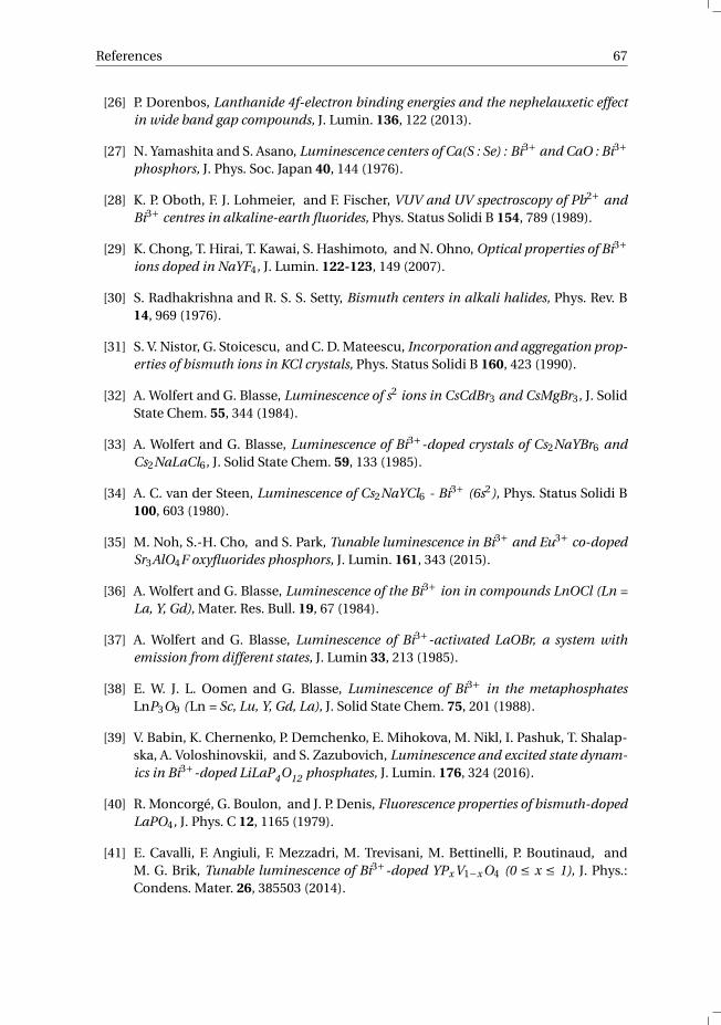
References 67
[26] P. Dorenbos, Lanthanide 4f-electron binding energies and the nephelauxetic effectin wide band gap compounds, J. Lumin. 136, 122 (2013).
[27] N. Yamashita and S. Asano, Luminescence centers of Ca(S : Se) : Bi3+ and CaO : Bi3+phosphors, J. Phys. Soc. Japan 40, 144 (1976).
[28] K. P. Oboth, F. J. Lohmeier, and F. Fischer, VUV and UV spectroscopy of Pb2+ andBi3+ centres in alkaline-earth fluorides, Phys. Status Solidi B 154, 789 (1989).
[29] K. Chong, T. Hirai, T. Kawai, S. Hashimoto, and N. Ohno, Optical properties of Bi3+ions doped in NaYF4, J. Lumin. 122-123, 149 (2007).
[30] S. Radhakrishna and R. S. S. Setty, Bismuth centers in alkali halides, Phys. Rev. B14, 969 (1976).
[31] S. V. Nistor, G. Stoicescu, and C. D. Mateescu, Incorporation and aggregation prop-erties of bismuth ions in KCl crystals, Phys. Status Solidi B 160, 423 (1990).
[32] A. Wolfert and G. Blasse, Luminescence of s2 ions in CsCdBr3 and CsMgBr3, J. SolidState Chem. 55, 344 (1984).
[33] A. Wolfert and G. Blasse, Luminescence of Bi3+-doped crystals of Cs2NaYBr6 andCs2NaLaCl6, J. Solid State Chem. 59, 133 (1985).
[34] A. C. van der Steen, Luminescence of Cs2NaYCl6 - Bi3+ (6s2), Phys. Status Solidi B100, 603 (1980).
[35] M. Noh, S.-H. Cho, and S. Park, Tunable luminescence in Bi3+ and Eu3+ co-dopedSr3AlO4F oxyfluorides phosphors, J. Lumin. 161, 343 (2015).
[36] A. Wolfert and G. Blasse, Luminescence of the Bi3+ ion in compounds LnOCl (Ln =La, Y, Gd), Mater. Res. Bull. 19, 67 (1984).
[37] A. Wolfert and G. Blasse, Luminescence of Bi3+-activated LaOBr, a system withemission from different states, J. Lumin 33, 213 (1985).
[38] E. W. J. L. Oomen and G. Blasse, Luminescence of Bi3+ in the metaphosphatesLnP3O9 (Ln = Sc, Lu, Y, Gd, La), J. Solid State Chem. 75, 201 (1988).
[39] V. Babin, K. Chernenko, P. Demchenko, E. Mihokova, M. Nikl, I. Pashuk, T. Shalap-ska, A. Voloshinovskii, and S. Zazubovich, Luminescence and excited state dynam-ics in Bi3+-doped LiLaP4O12 phosphates, J. Lumin. 176, 324 (2016).
[40] R. Moncorgé, G. Boulon, and J. P. Denis, Fluorescence properties of bismuth-dopedLaPO4, J. Phys. C 12, 1165 (1979).
[41] E. Cavalli, F. Angiuli, F. Mezzadri, M. Trevisani, M. Bettinelli, P. Boutinaud, andM. G. Brik, Tunable luminescence of Bi3+-doped YPx V1−x O4 (0 ≤ x ≤ 1), J. Phys.:Condens. Mater. 26, 385503 (2014).
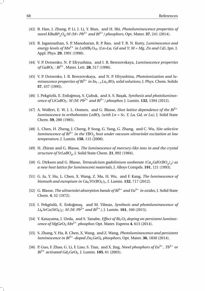
68 References
[42] B. Han, J. Zhang, P. Li, J. Li, Y. Bian, and H. Shi, Photoluminescence properties ofnovel KBaBP2O8:M (M= Pb2+ and Bi3+) phosphors, Opt. Mater. 37, 241 (2014).
[43] R. Jagannathan, S. P. Manoharan, R. P. Rao, and T. R. N. Kutty, Luminescence andenergy levels of Mn2+ in LnMB5O10 (Ln=La, Gd and Y; M = Mg, Zn and Cd), Jpn. J.Appl. Phys. 29, 1991 (1990).
[44] V. P. Dotsenko, N. P. Efryushina, and I. B. Berezovskaya, Luminescence propertiesof GaBO3 : Bi3+, Mater. Lett. 28, 517 (1996).
[45] V. P. Dotsenko, I. B. Berezovskaya, and N. P. Efryushina, Photoionization and lu-minescence properties of Bi3+ in In1−x Lux BO3 solid solutions, J. Phys. Chem. Solids57, 437 (1995).
[46] I. Pekgözlü, E. Erdogmus, S. Çubuk, and A. S. Basak, Synthesis and photolumines-cence of LiCaBO3: M (M: Pb2+ and Bi3+) phosphor, J. Lumin. 132, 1394 (2012).
[47] A. Wolfert, E. W. J. L. Oomen, and G. Blasse, Host lattice dependence of the Bi3+luminescence in orthoborates LnBO3 (with Ln = Sc, Y, La, Gd, or Lu), J. Solid StateChem. 59, 280 (1985).
[48] L. Chen, H. Zheng, J. Cheng, P. Song, G. Yang, G. Zhang, and C. Wu, Site-selectiveluminescence of Bi3+ in the YBO3 host under vacuum ultraviolet excitation at lowtemperature, J. Lumin. 158, 115 (2008).
[49] H. Zhiran and G. Blasse, The luminescence of mercury-like ions in and the crystalstructure of SrLaBO4, J. Solid State Chem. 21, 892 (1984).
[50] G. Dirksen and G. Blasse, Tetracalcium gadolinium oxoborate (Ca4GdO(BO3)3) asa new host lattice for luminescent materials, J. Alloys Compds. 191, 121 (1993).
[51] G. Ju, Y. Hu, L. Chen, X. Wang, Z. Mu, H. Wu, and F. Kang, The luminescence ofbismuth and europium in Ca4YO(BO3)3, J. Lumin. 132, 717 (2012).
[52] G. Blasse, The ultraviolet absorption bands of Bi3+ and Eu3+ in oxides, J. Solid StateChem. 4, 52 (1972).
[53] I. Pekgözlü, E. Erdogmus, and M. Yilmaz, Synthesis and photoluminescence ofLi4SrCa(SiO4)2: M (M: Pb2+ and Bi3+), J. Lumin. 161, 160 (2015).
[54] Y. Katayama, J. Ueda, and S. Tanabe, Effect of Bi2O3 doping on persistent lumines-cence of MgGeO3:Mn2+ phosphor, Opt. Mater. Express 4, 613 (2014).
[55] S. Zhang, Y. Hu, R. Chen, X. Wang, and Z. Wang, Photoluminescence and persistentluminescence in Bi3+-doped Zn2GeO4 phosphors, Opt. Mater. 36, 1830 (2014).
[56] P. Guo, F. Zhao, G. Li, F. Liao, S. Tian, and X. Jing, Novel phosphors of Eu3+, Tb3+ orBi3+ activated Gd2GeO5, J. Lumin. 105, 61 (2003).
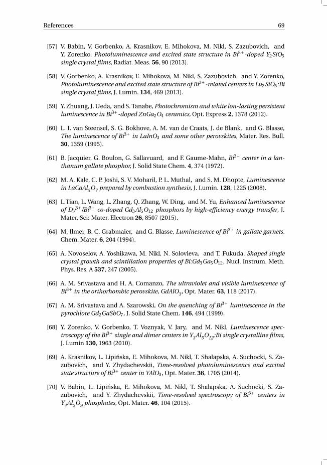
References 69
[57] V. Babin, V. Gorbenko, A. Krasnikov, E. Mihokova, M. Nikl, S. Zazubovich, andY. Zorenko, Photoluminescence and excited state structure in Bi3+-doped Y2SiO5
single crystal films, Radiat. Meas. 56, 90 (2013).
[58] V. Gorbenko, A. Krasnikov, E. Mihokova, M. Nikl, S. Zazubovich, and Y. Zorenko,Photoluminescence and excited state structure of Bi3+-related centers in Lu2SiO5:Bisingle crystal films, J. Lumin. 134, 469 (2013).
[59] Y. Zhuang, J. Ueda, and S. Tanabe, Photochromism and white lon-lasting persistentluminescence in Bi3+-doped ZnGa2O4 ceramics, Opt. Express 2, 1378 (2012).
[60] L. I. van Steensel, S. G. Bokhove, A. M. van de Craats, J. de Blank, and G. Blasse,The luminescence of Bi3+ in LaInO3 and some other perovskites, Mater. Res. Bull.30, 1359 (1995).
[61] B. Jacquier, G. Boulon, G. Sallavuard, and F. Gaume-Mahn, Bi3+ center in a lan-thanum gallate phosphor, J. Solid State Chem. 4, 374 (1972).
[62] M. A. Kale, C. P. Joshi, S. V. Moharil, P. L. Muthal, and S. M. Dhopte, Luminescencein LaCaAl3O7 prepared by combustion synthesis, J. Lumin. 128, 1225 (2008).
[63] L.Tian, L. Wang, L. Zhang, Q. Zhang, W. Ding, and M. Yu, Enhanced luminescenceof Dy3+/Bi3+ co-doped Gd3Al5O12 phosphors by high-efficiency energy transfer, J.Mater. Sci: Mater. Electron 26, 8507 (2015).
[64] M. Ilmer, B. C. Grabmaier, and G. Blasse, Luminescence of Bi3+ in gallate garnets,Chem. Mater. 6, 204 (1994).
[65] A. Novoselov, A. Yoshikawa, M. Nikl, N. Solovieva, and T. Fukuda, Shaped singlecrystal growth and scintillation properties of Bi:Gd3Ga5O12, Nucl. Instrum. Meth.Phys. Res. A 537, 247 (2005).
[66] A. M. Srivastava and H. A. Comanzo, The ultraviolet and visible luminescence ofBi3+ in the orthorhombic perovskite, GdAlO3, Opt. Mater. 63, 118 (2017).
[67] A. M. Srivastava and A. Szarowski, On the quenching of Bi3+ luminescence in thepyrochlore Gd2GaSbO7, J. Solid State Chem. 146, 494 (1999).
[68] Y. Zorenko, V. Gorbenko, T. Voznyak, V. Jary, and M. Nikl, Luminescence spec-troscopy of the Bi3+ single and dimer centers in Y3Al5O12:Bi single crystalline films,J. Lumin 130, 1963 (2010).
[69] A. Krasnikov, L. Lipinska, E. Mihokova, M. Nikl, T. Shalapska, A. Suchocki, S. Za-zubovich, and Y. Zhydachevskii, Time-resolved photoluminescence and excitedstate structure of Bi3+ center in YAlO3, Opt. Mater. 36, 1705 (2014).
[70] V. Babin, L. Lipinska, E. Mihokova, M. Nikl, T. Shalapska, A. Suchocki, S. Za-zubovich, and Y. Zhydachevskii, Time-resolved spectroscopy of Bi3+ centers inY4Al2O9 phosphates, Opt. Mater. 46, 104 (2015).
70 References
[71] V. Babin, V. Gorbenko, A. Krasnikov, A. Makhov, M. Nikl, K. Polak, S. Zazubovich,and Y. Zorenko, Peculiarities of excited state structure and photoluminescence inBi3+-doped Lu3Al5O12 single-crystalline films, J. Phys.: Condens. Matter 21, 415502(2009).
[72] Y. Zorenko, M. Pashkovsky, A. Voloshinovskii, B. Kuklinski, and M. Grinberg, Theluminescence of CaWO4 single crystals, J. Lumin 116, 43 (2006).
[73] L. Wang, Z. Lv, W. Kang, X. Shangguan, J. Shi, and Z. Hao, Applications orienteddesign of Bi3+ doped phosphors, Appl. Phys. Lett. 102, 151909 (2013).
[74] G. Boulon, Processus de photoluminescence dans les oxydes et les orthovanadatesde terres rares polycristallins actives par l’ion Bi3+, J. Phys. (Paris) 32, 333 (1971).
[75] F. Kang, M. Peng, Q. Zhang, and J. Qiu, Abnormal anti-quenching and control-lable multi-transitions of Bi3+ luminescence by temperature in a yellow-emittingLuVO4:Bi3+ phosphor for UV-converted white LEDs, Chem. Eur. J. 20, 11522 (2014).
[76] F. Kang, X. Yang, M. Peng, L. Wondraczek, Z. Ma, Q. Zhang, and J. Qiu, Red pho-toluminescence from Bi3+ and the influence of the oxygen-vacancy perturbation inScVO4: A combined experimental and theoretical study, J. Phys. Chem. C 118, 7515(2014).
[77] T. K. Park, H. C. Ahn, and S. I. Mho, High concentration of Bi3+ incorporated intoRNbO4:Eu3+ (R = La, Y, Gd) as red phosphors for white LED applications, J. KoreanPhys. Soc. 52, 431 (2008).
[78] X. M. Liu and J. Lin, Enhanced luminescence of gadolinium niobates by Bi3+ dopingfor field effect emission displays, J. Lumin. 122-123, 700 (2007).
[79] S. H. Shin, D. Y. Jeon, and K. S. Suh, Charge-transfer nature in luminescence ofYNbO4:Bi blue phosphor, J. Appl. Phys. 90, 5986 (2001).
[80] S. I. Kubota, H. Yamane, and M. Shimada, Luminescence properties ofGd1−x Bix Ta7O19, J. Alloys Compds. 281, 181 (1998).
[81] G. Blasse and A. Bril, Luminescence phenomena in compounds with fergusonitestructure, J. Lumin. 3, 109 (1970).
[82] P. Boutinaud, E. Cavalli, and R. Mahiou, Photon conversion in Bi3+/Pr3+-codopedCaTiO3, J. Phys.: Condens. Matter 24, 295502 (2012).
[83] A. M. Srivastava, H. A. Comanzo, and S. J. Camaradello, On the Bi3+ - Ti4+ chargetransfer transition in the pyrochlore Y2Ti2O7 : Bi3+, Opt. Mater. 48, 31 (2015).
[84] D. R. Taikar, C. P. Joshi, S. V. Moharil, P. L. Muthal, and S. M. Dhopte, Synthesis andluminescence of SrZnO2 phosphors, J. Lumin. 130, 1690 (2010).
[85] A. F. Ellervee, Luminescence of Pb2+ and Bi3+ centres in alkali-earth sulphides andoxides, Phys. Status Solidi B 82, 91 (1977).
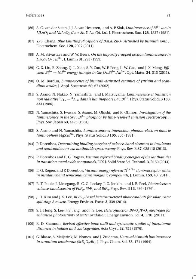
References 71
[86] A. C. van der Steen, J. J. A. van Hesteren, and A. P. Slok, Luminescence of Bi3+ ion inLiLnO2 and NaLnO2 (Ln = Sc, Y, La, Gd, Lu), J. Electrochem. Soc. 128, 1327 (1981).
[87] Y.-S. Chang, Blue Emitting Phosphors of BaLa2ZnO5 Activated by Bismuth ions, J.Electrochem. Soc. 128, 2027 (2011).
[88] A. M. Srivastava and W. W. Beers, On the impurity trapped exciton luminescence inLa2Zr2O7 : Bi3+, J. Lumin 81, 293 (1999).
[89] G. X. Liu, R. Zhang, Q. L. Xiao, S. Y. Zou, W. F. Peng, L. W. Cao, and J. X. Meng, Effi-cient Bi3+ → Nd3+ energy transfer in Gd2O3:Bi3+,Nd3+, Opt. Mater. 34, 313 (2011).
[90] O. M. Bordun, Luminescence of bismuth-activated ceramics of yttrium and scan-dium oxides, J. Appl. Spectrosc. 69, 67 (2002).
[91] S. Asano, N. Nakao, N. Yamashita, and I. Matsuyama, Luminescence et transitionnon radiative 3T1u → 3A1u dans le luminophore BaS:Bi3+, Phys. Status Solidi B 133,333 (1986).
[92] N. Yamashita, S. Iwasaki, S. Asano, M. Ohishi, and K. Ohmori, Investigation of theluminescence in the SrS : Bi3+ phosphor by time-resolved emission spectroscopy, J.Phys. Soc. Japan 53, 4425 (1984).
[93] S. Asano and N. Yamashita, Luminescence et interaction phonon-electron dans leluminophore MgS:Bi3+, Phys. Status Solidi B 105, 305 (1981).
[94] P. Dorenbos, Determining binding energies of valence-band electrons in insulatorsand semiconductors via lanthanide spectroscopy, Phys. Rev. B 87, 035118 (2013).
[95] P. Dorenbos and E. G. Rogers, Vacuum referred binding energies of the lanthanidesin transition metal oxide compounds, ECS J. Solid State Sci. Technol. 3, R150 (2014).
[96] E. G. Rogers and P. Dorenbos, Vacuum energy referred Ti3+/4+ donor/acceptor statesin insulating and semiconducting inorganic compounds, J. Lumin. 153, 40 (2014).
[97] R. T. Poole, J. Liesegang, R. C. G. Leckey, J. G. Jenkin, and J. B. Peel, Photoelectronvalence-band spectra of PbF2, SbF3 and BiF3, Phys. Rev. B 13, 896 (1976).
[98] J. H. Kim and J. S. Lee, BiVO4-based heterostructered photocatalysts for solar watersplitting: A review, Energy Environ. Focus 3, 339 (2014).
[99] S. J. Hong, S. Lee, J. S. Jang, and J. S. Lee, Heterojunction BiVO4/WO3 electrodes forenhanced photoactivity of water oxidation, Energy Environ. Sci. 4, 1781 (2011).
[100] R. D. Shannon, Revised effective ionic radii and systematic studies of interatomicdistances in halides and chalcogenides, Acta Cryst. 32, 751 (1976).
[101] G. Blasse, A. Meijerink, M. Nomes, and J. Zuidema, Unusual bismuth luminescencein strontium tetraborate (SrB4O7:Bi), J. Phys. Chem. Sol. 55, 171 (1994).
72 References
[102] A. M. Srivastava, Luminescence of divalent bismuth in M2+BPO5 (M2+ = Ba2+, Sr2+and Ca2+, J. Lumin. 78, 239 (1998).
[103] R. Cao, M. Peng, and J. Qiu, Photoluminescence of Bi2+-doped BaSO4 as a red phos-phor for white LEDs, Opt. Express 20, A977 (2012).
[104] B. Jacquier, Photoluminescence processes in LaOCl:Bi and YOCl:Bi, J. Lumin. 10, 95(1975).
[105] W. Zhang, S. Liu, Z. Hu, Y. Lian, Z. Feng, and X. Sheng, Preparation ofYBO3:Dy3+,Bi3+ phosphors and enhance photoluminescence, Mater. Sci. Eng. B187, 108 (2014).
[106] A. M. Srivastava, Luminescence of Bi3+ in LaGaO3, Mater. Res. Bull. 34, 1391 (1999).
[107] A. C. van der Steen and L. T. F. Dijcks, The luminescence properties of alkaline-earthoxides activated with 6s2 ions, Phys. Status Solidi B 104, 283 (1981).
[108] A. M. van de Craats and G. Blasse, The quenching of bismuth(III) luminescence inyttrium oxide Y2O3, Chem. Phys. Lett. 243, 559 (1995).
6Towards a general concentration
quenching model of Bi3+ luminescence
The vacuum referred binding energy of the electron in the Bi2+ ground state has been de-termined in 15 different compounds. This shows that the electron binding energy in theground state of Bi2+ is at lower (more negative) energy compared to the electron bindingenergy in the excited state of Bi3+. This means that electron transfer from the excitedstate of one Bi3+ to a neighboring Bi3+, forming a Bi2+–Bi4+ pair, acts as a quenchingroute for the Bi3+ emission. Electron back transfer in the Bi2+–Bi4+ pair is then sug-gested to be the origin for the frequently observed pair emission. This paper shows thatvacuum referred electron binding energy diagrams can provide a unique physical insightin the properties of inorganic compounds.
This chapter is based on the publication: R. H. P. Awater and P. Dorenbos, “Towards ageneral concentration quenching model of Bi3+ luminescence”, Journal of Luminescence188 (2017), 487.
73
74 6. Towards a general concentration quenching model of Bi3+ luminescence
6.1. IntroductionBi3+ shows a complex temperature and concentration dependent luminescence quench-ing [1–3]. The luminescence quenching cannot be explained by multi-phonon relax-ation because of a too large energy gap between the 3P1 excited state and the 1S0 groundstate. A transfer of an electron from the excited state to the conduction band is oftenused to describe the quenching, like for example in (In,Lu)BO3 and Ca(Zr,Sn)O3 com-pounds [4, 5]. Another possibility for luminescence quenching is via the charge transfer(CT) of an electron in the valence band to a bismuth ion as has been proposed for ex-ample in LaOBr [6]. These two quenching routes involving CT apply to isolated bismuthcenters. A third type of quenching occurs in Bi-pairs, which becomes important at highconcentrations of bismuth or in the case of preferential formation of bismuth pairs orclusters [7–9]. The mechanism of such type of quenching has always remained open.
- 1 5- 1 4- 1 3- 1 2- 1 1- 1 0
- 9- 8- 7- 6- 5- 4- 3- 2- 1012
3 P 1
1 S 0
CaSe
YVO 4
YNbO
4
YTaO
4
Y 2O3
YAlO 3
VRBE
(eV)
YPO 4
E X
E V
E C
CaF 2
CaO
CaS
Figure 6.1: Stacked VRBE diagrams for 10 different Bi3+ doped compounds with EC the binding energy at theconduction band bottom, EV the binding energy at the valence band top and EX the binding energy in theexciton state. The blue bars labeled 1S0 and 3P1 indicate the electron binding energy in the Bi3+ ground andexcited state, respectively.
In chapter 5 we determined the vacuum referred electron binding energies (VRBE)in the Bi3+ [
1S0]
and[
3P1]
levels in 44 different compounds. The VRBE of Bi3+ in a se-lection of 10 of those compounds is shown in Fig. 6.1. The VRBE in the 1S0 ground statevaries between −5 and −10 eV and in the 3P1 excited state between −2 and −4 eV in asystematic fashion with the chemical and structural properties of the compound. WhenBi3+ is doped in compounds with a low lying conduction band, e.g. compounds con-taining transition metals with d0 configuration such as YNbO4 and YVO4 in Fig. 6.1, the3P1 excited state appears above the conduction band (CB) bottom. In these cases pho-toionization to the CB occurs without generating any Bi3+ emission. In stead a MMCTemission is often observed in these compounds [10, 11]. Besides Bi3+, also luminescencefrom Bi2+ has been reported in fluorides, phosphates, sulphates and borates [12–15]. For
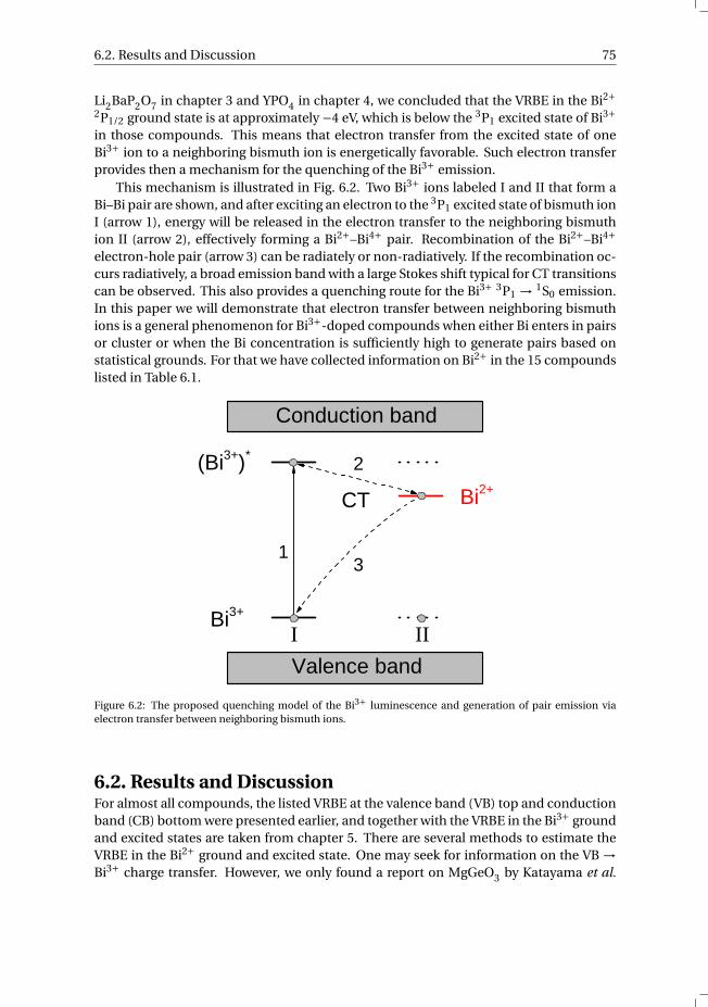
6.2. Results and Discussion 75
Li2BaP2O7 in chapter 3 and YPO4 in chapter 4, we concluded that the VRBE in the Bi2+2P1/2 ground state is at approximately −4 eV, which is below the 3P1 excited state of Bi3+in those compounds. This means that electron transfer from the excited state of oneBi3+ ion to a neighboring bismuth ion is energetically favorable. Such electron transferprovides then a mechanism for the quenching of the Bi3+ emission.
This mechanism is illustrated in Fig. 6.2. Two Bi3+ ions labeled I and II that form aBi–Bi pair are shown, and after exciting an electron to the 3P1 excited state of bismuth ionI (arrow 1), energy will be released in the electron transfer to the neighboring bismuthion II (arrow 2), effectively forming a Bi2+–Bi4+ pair. Recombination of the Bi2+–Bi4+electron-hole pair (arrow 3) can be radiately or non-radiatively. If the recombination oc-curs radiatively, a broad emission band with a large Stokes shift typical for CT transitionscan be observed. This also provides a quenching route for the Bi3+ 3P1 → 1S0 emission.In this paper we will demonstrate that electron transfer between neighboring bismuthions is a general phenomenon for Bi3+-doped compounds when either Bi enters in pairsor cluster or when the Bi concentration is sufficiently high to generate pairs based onstatistical grounds. For that we have collected information on Bi2+ in the 15 compoundslisted in Table 6.1.
31
2
I II
C T
V a l e n c e b a n d
C o n d u c t i o n b a n d
B i 3 +
B i 2 +( B i 3 + ) *
Figure 6.2: The proposed quenching model of the Bi3+ luminescence and generation of pair emission viaelectron transfer between neighboring bismuth ions.
6.2. Results and DiscussionFor almost all compounds, the listed VRBE at the valence band (VB) top and conductionband (CB) bottom were presented earlier, and together with the VRBE in the Bi3+ groundand excited states are taken from chapter 5. There are several methods to estimate theVRBE in the Bi2+ ground and excited state. One may seek for information on the VB →Bi3+ charge transfer. However, we only found a report on MgGeO3 by Katayama et al.
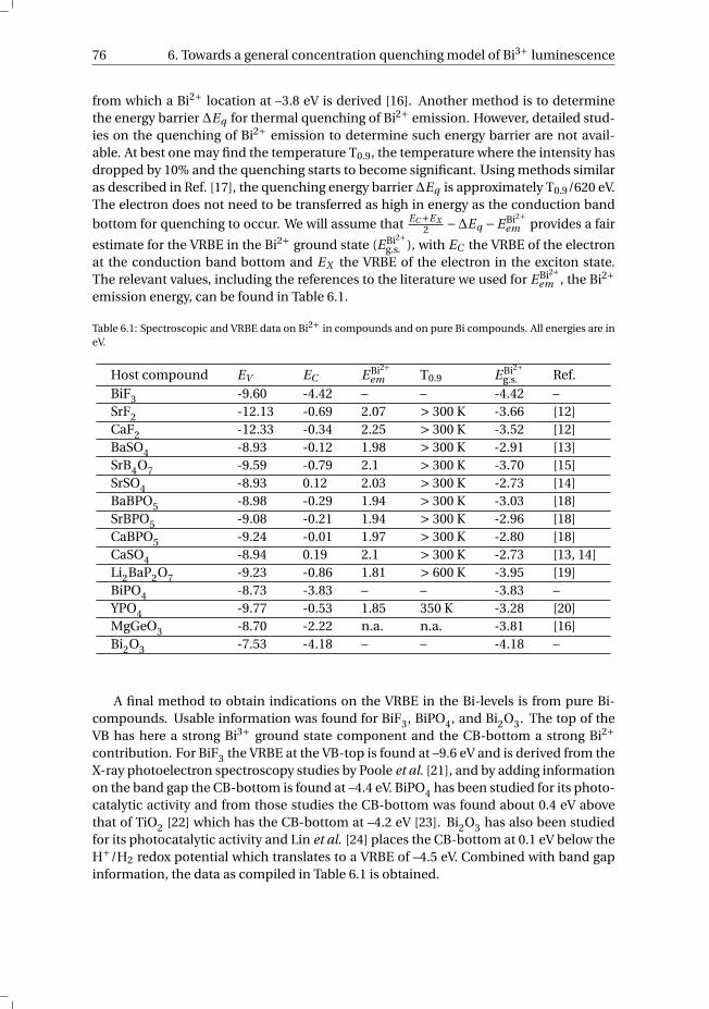
76 6. Towards a general concentration quenching model of Bi3+ luminescence
from which a Bi2+ location at –3.8 eV is derived [16]. Another method is to determinethe energy barrier ∆Eq for thermal quenching of Bi2+ emission. However, detailed stud-ies on the quenching of Bi2+ emission to determine such energy barrier are not avail-able. At best one may find the temperature T0.9, the temperature where the intensity hasdropped by 10% and the quenching starts to become significant. Using methods similaras described in Ref. [17], the quenching energy barrier∆Eq is approximately T0.9/620 eV.The electron does not need to be transferred as high in energy as the conduction band
bottom for quenching to occur. We will assume that EC+EX2 −∆Eq −E Bi2+
em provides a fair
estimate for the VRBE in the Bi2+ ground state (E Bi2+g.s. ), with EC the VRBE of the electron
at the conduction band bottom and EX the VRBE of the electron in the exciton state.The relevant values, including the references to the literature we used for E Bi2+
em , the Bi2+emission energy, can be found in Table 6.1.
Table 6.1: Spectroscopic and VRBE data on Bi2+ in compounds and on pure Bi compounds. All energies are ineV.
Host compound EV EC E Bi2+em T0.9 E Bi2+
g.s. Ref.BiF3 -9.60 -4.42 – – -4.42 –SrF2 -12.13 -0.69 2.07 > 300 K -3.66 [12]CaF2 -12.33 -0.34 2.25 > 300 K -3.52 [12]BaSO4 -8.93 -0.12 1.98 > 300 K -2.91 [13]SrB4O7 -9.59 -0.79 2.1 > 300 K -3.70 [15]SrSO4 -8.93 0.12 2.03 > 300 K -2.73 [14]BaBPO5 -8.98 -0.29 1.94 > 300 K -3.03 [18]SrBPO5 -9.08 -0.21 1.94 > 300 K -2.96 [18]CaBPO5 -9.24 -0.01 1.97 > 300 K -2.80 [18]CaSO4 -8.94 0.19 2.1 > 300 K -2.73 [13, 14]Li2BaP2O7 -9.23 -0.86 1.81 > 600 K -3.95 [19]BiPO4 -8.73 -3.83 – – -3.83 –YPO4 -9.77 -0.53 1.85 350 K -3.28 [20]MgGeO3 -8.70 -2.22 n.a. n.a. -3.81 [16]Bi2O3 -7.53 -4.18 – – -4.18 –
A final method to obtain indications on the VRBE in the Bi-levels is from pure Bi-compounds. Usable information was found for BiF3, BiPO4, and Bi2O3. The top of theVB has here a strong Bi3+ ground state component and the CB-bottom a strong Bi2+contribution. For BiF3 the VRBE at the VB-top is found at –9.6 eV and is derived from theX-ray photoelectron spectroscopy studies by Poole et al. [21], and by adding informationon the band gap the CB-bottom is found at –4.4 eV. BiPO4 has been studied for its photo-catalytic activity and from those studies the CB-bottom was found about 0.4 eV abovethat of TiO2 [22] which has the CB-bottom at –4.2 eV [23]. Bi2O3 has also been studiedfor its photocatalytic activity and Lin et al. [24] places the CB-bottom at 0.1 eV below theH+/H2 redox potential which translates to a VRBE of –4.5 eV. Combined with band gapinformation, the data as compiled in Table 6.1 is obtained.
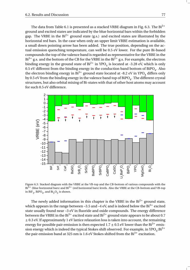
6.2. Results and Discussion 77
The data from Table 6.1 is presented as a stacked VRBE diagram in Fig. 6.3. The Bi3+ground and excited states are indicated by the blue horizontal bars within the forbiddengap. The VRBE in the Bi2+ ground state (g.s.) and excited states are illustrated by thehorizontal red bars. In the case when only an upper limit VRBE estimation is available,a small down pointing arrow has been added. The true position, depending on the ac-tual emission quenching temperature, can well be 0.5 eV lower. For the pure Bi-basedcompounds the top of the valence band is regarded as representative for the VRBE in theBi3+ g.s. and the bottom of the CB for the VRBE in the Bi2+ g.s. For example, the electronbinding energy in the ground state of Bi2+ in YPO4 is located at -3.28 eV, which is only0.5 eV different from the binding energy in the conduction band bottom of BiPO4. Alsothe electron binding energy in Bi3+ ground state located at -8.2 eV in YPO4 differs onlyby 0.5 eV from the binding energy in the valence band top of BiPO4. The different crystalstructures, but also orbital mixing of Bi-states with that of other host atoms may accountfor such 0.5 eV difference.
- 1 5- 1 4- 1 3- 1 2- 1 1- 1 0
- 9- 8- 7- 6- 5- 4- 3- 2- 1012
BaBP
O 5
SrBPO
5
SrB4O
7
CaBP
O 5
BaSO
4
SrSO 4
CaSO
4
Bi 2O3
MgGe
O 3
Li 2BaP 2O
7
BiPO 4
BiF3
SrF2
CaF 2
VRBE
(eV)
YPO 4
Figure 6.3: Stacked diagram with the VRBE at the VB-top and the CB-bottom of various compounds with theBi3+ (blue horizontal bars) and Bi2+ (red horizontal bars) levels. Also the VRBE at the CB-bottom and VB-topin BiF3, BiPO4, and Bi2O3 is shown.
The newly added information in this chapter is the VRBE in the Bi2+ ground state,which appears in the range between –3.5 and –4 eV, and is indeed below the Bi3+ excitedstate usually found near –3 eV in fluoride and oxide compounds. The energy differencebetween the VRBE in the Bi3+ excited state and Bi2+ ground state appears to be about 0.7± 0.3 eV. If approximately 1 eV lattice relaxation loss is taken into account, the remainingenergy for possible pair emission is then expected 1.7 ± 0.5 eV lower than the Bi3+ emis-sion energy which is indeed the typical Stokes shift observed. For example, in YPO4:Bi3+the pair emission band at 325 nm is 1.6 eV Stokes shifted from the Bi3+ excitation.
78 References
Depending on the transition rates, complicated dynamics as in the Bi3+-doped gar-net systems may now occur [25–27]. It is not the purpose of this work to enter in toomuch detail but some general ideas can be launched. The typical luminescence decayrate at room temperature of the Bi3+ emission is found near 1 µs and the luminescencedecay of the pair emission is typically 100 µs [27, 28]. The radiative decay rate of the Bi3+emission (arrow 1 in Fig. 6.2) has to compete with the electron transfer rate to the neigh-boring Bi ion (arrow 2 in Fig. 6.2). In such electron transfer, the above found 0.7 ± 0.3 eVenergy difference needs to be emitted as phonons and a temperature dependent rate isto be expected. Once in the Bi4+–Bi2+ pair state, again different rates apply. With only 0.7eV difference, thermally activated electron back transfer to the higher energy Bi3+[
3P1]–
Bi3+[1S0
]pair state is possible (reverse of arrow 2 in Fig. 6.2). In addition, there are the
luminescence decay rates of Bi-pair emission, and its thermal quenching rate.Srivastava et al. [2] studied the luminescence intensity as function of temperature of
the Bi3+ emission at 385 nm (3.22 eV) and observed an additional emission band labeledas VIS-band at 514 nm (2.41 eV) when exciting Bi3+ at 290 nm (4.27 eV) in 0.5% Bi3+doped La2Zr2O7. From 0 K to 60 K the Bi3+ emission quenches whereas the VIS-bandgrows in intensity, and from 70 K to 120 K the process is reversed and the Bi3+ emissiongrows again with decreasing VIS-band intensity. Above 120 K both bands quench untilat RT no emission remains. Although the origin of the VIS-band was not clear, one mayalso interpret it as Bi-pair emission. Intensity first grows at the expense of Bi3+ emis-sion, above 70 K electron back transfer to the Bi3+ excited state reverses the process, andabove 120 K the radiation-less electron transfer to the Bi3+ ground state starts to quenchboth emissions. Energetically such processes are well-possible. More detailed studieson the luminescence dynamics as function of temperature and Bi concentration wouldbe required to verify or falsify such dynamics.
6.3. ConclusionWe have shown that in general the VRBE in the Bi2+ ground state is located at lower en-ergy as compared to the VRBE in the Bi3+ 3P1 excited state. In the presence of Bi–Bi pairs,it is then upon excitation of one Bi3+ energetically favorable for electron transfer to oc-cur, and to form a Bi2+–Bi4+ pair. Based on the estimated VRBEs in the Bi2+ ground statein 15 different compounds, the electron transfer between neighboring Bi ions appearsalways energetically possible. The recombination of the electron and hole on the Bi2+–Bi4+ pair can occur non-radiatively or radiatively, in the later case the resulting visibleemission band is often observed and ascribed to pair emission. The proposed mech-anism of charge transfer between Bi-pairs can also explain the quenching behavior ofBi3+ luminescence when the Bi3+ concentration increases.
References[1] A. M. Srivastava and S. J. Camardello, Concentration dependence of the Bi3+ lumi-
nescence in LnPO4 (Ln = Y3+, Lu3+), Opt. Mater. 39, 130 (2015).
[2] A. M. Srivastava and W. W. Beers, On the impurity trapped exciton luminescence inLa2Zr2O7 : Bi3+, J. Lumin 81, 293 (1999).
References 79
[3] A. M. Srivastava and A. Szarowski, On the quenching of Bi3+ luminescence in thepyrochlore Gd2GaSbO7, J. Solid State Chem. 146, 494 (1999).
[4] V. P. Dotsenko, I. B. Berezovskaya, and N. P. Efryushina, Photoionization and lumi-nescence properties of Bi3+ in In1−x Lux BO3 solid solutions, J. Phys. Chem. Solids 57,437 (1995).
[5] A. M. Srivastava, Luminescence of Bi3+ in the orthorhombic perovskites CaB4+O3
(B4+=Zr, Sn): crossover from localized to D-state emission, Opt. Mater. 58, 89 (2016).
[6] A. Wolfert and G. Blasse, Luminescence of Bi3+-activated LaOBr, a system with emis-sion from different states, J. Lumin 33, 213 (1985).
[7] H. Zhiran and G. Blasse, Energy transfer phenomena in luminescent materials basedon GdB3O6, Mater. Chem. Phys. 12, 257 (1985).
[8] A. M. Srivastava, On the luminescence of Bi3+ in the pyrochlore Y2Sn2O7, Mater. Res.Bull 37, 745 (2002).
[9] A. M. Srivastava and H. A. Comanzo, The ultraviolet and visible luminescence of Bi3+in the orthorhombic perovskite, GdAlO3, Opt. Mater. 63, 118 (2017).
[10] P. Boutinaud, Revisiting the spectroscopy of the Bi3+ ion in oxide compounds, Inorg.Chem. 52, 6028 (2013).
[11] G. Blasse, Optical electron transfer between metal ions and its consequences, Struct.Bonding 76, 153 (1991).
[12] R. Cao, F. Zhang, C. Liao, and J. Qiu, Yellow-to-orange emission from Bi2+-dopedRF2 (R = Ca and Sr) phosphors, Opt. Express 21, 15728 (2013).
[13] R. Cao, M. Peng, and J. Qiu, Photoluminescence of Bi2+-doped BaSO4 as a red phos-phor for white LEDs, Opt. Express 20, A977 (2012).
[14] M. A. Hamstra, H. F. Folkerts, and G. Blasse, Red Bismuth Emission in Alkaline-earthmetal Sulfates, J. Mater. Chem. 4, 1349 (1994).
[15] G. Blasse, A. Meijerink, M. Nomes, and J. Zuidema, Unusual bismuth luminescencein strontium tetraborate (SrB4O7:Bi), J. Phys. Chem. Sol. 55, 171 (1994).
[16] Y. Katayama, J. Ueda, and S. Tanabe, Effect of Bi2O3 doping on persistent lumines-cence of MgGeO3:Mn2+ phosphor, Opt. Mater. Express 4, 613 (2014).
[17] P. Dorenbos, Thermal quenching of Eu2+ 5d–4f luminescence in inorganic com-pounds, J. Phys.: Condens. Matter 17, 8103 (2005).
[18] M. Peng and L. Wondraczek, Bi2+-doped strontium borates for white-light emittingdiodes, Opt. Lett. 34, 2885 (2009).
[19] R. H. P. Awater and P. Dorenbos, X-ray induced valence change and vacuum referredbinding energies of Bi3+ and Bi2+ in Li2BaP2O7, J. Phys. Chem. C 120, 15114 (2016).
80 References
[20] R. H. P. Awater, L. C. Niemeijer-Berghuijs, and P. Dorenbos, Luminescence andcharge carrier trapping in YPO4:Bi, Opt. Mater. 66, 351 (2017).
[21] R. T. Poole, J. Liesegang, R. C. G. Leckey, J. G. Jenkin, and J. B. Peel, Photoelectronvalence-band spectra of PbF2, SbF3 and BiF3, Phys. Rev. B 13, 896 (1976).
[22] C. Pan and Y. Zhu, New type of BiPO4 oxy-acid salt photocatalyst with high photo-catalytic activity on degradation of dye, Environ. Sci. Technol. 44, 5570 (2010).
[23] P. Dorenbos, The electronic structure of lanthanide impurities in TiO2, ZnO, SnO2,and related compounds, ECS J. Solid State Sci. Technol. 3, R19 (2014).
[24] X. Lin, J. Xin, W. Wang, Z. Shan, F. Xu, and F. Huang, Photocatalytic activities ofheterojunction semiconductors Bi2O3/BaTiO3: A strategy for the design of efficientcombined photocatalysts, J. Phys. Chem. C 111, 18288 (2007).
[25] Y. Zorenko, V. Gorbenko, T. Voznyak, V. Jary, and M. Nikl, Luminescence spectroscopyof the Bi3+ single and dimer centers in Y3Al5O12:Bi single crystalline films, J. Lumin130, 1963 (2010).
[26] V. Babin, V. Gorbenko, A. Krasnikov, A. Makhov, M. Nikl, K. Polak, S. Zazubovich,and Y. Zorenko, Peculiarities of excited state structure and photoluminescence inBi3+-doped Lu3Al5O12 single-crystalline films, J. Phys.: Condens. Matter 21, 415502(2009).
[27] V. Babin, V. Gorbenko, A. Krasnikov, A. Makhov, E. Mihokova, M. Nikl, S. Za-zubovich, and Y. Zorenko, Origin of Bi3+-related luminescence centres in Lu3Al5O12
and Y3Al5O12 single crystalline films and the structure of their relaxed excited states,Phys. Status Solidi B 249, 1039 (2012).
[28] G. Blasse and A. Bril, Investigations of Bi3+-activated phosphors, J. Chem. Phys. 48,217 (1968).
7The vacuum referred electron binding
energies in the 1S0 and 3P1 states of Pb2+
and Tl+ in inorganic compounds
An overview of the spectroscopic data on Tl+ and Pb2+ in 37 and 126 different inorganiccompounds, respectively, is presented. Using the metal-to-metal charge transfer andA-band transition energies, the electron binding energies in the 1S0 ground state and3P1 excited state of Tl+ and Pb2+ were determined relative to the vacuum level. By con-structing vacuum referred binding energy (VRBE) diagrams that display the energy levelsof the Tl+ and Pb2+ activator ion together with that of the host compound, insight in theluminescent properties of these activated compounds are gained. The obtained VRBEsof the electron in the 1S0 and 3P1 states of Tl+ and Pb2+ are compared to those of Bi3+.
This chapter is based on the publication that has been submitted to Journal of Lumines-cence: R. H. P. Awater and P. Dorenbos, “The vacuum referred electron binding energiesin the 1S0 and 3P1 states of Pb2+ and Tl+ in inorganic compounds”.
81
82 The VRBEs in the 1S0 and 3P1 states of Pb2+ and Tl+
7.1. Introduction
The continuous research on Ce3+-doped halides for scintillation materials led to the dis-covery of LaBr3:Ce,Sr. It has an energy resolution of 2% for the detection of 662 keVγ-photons and a light yield of 70.000 photons per MeV of ionization energy [1]. Despitethese excellent scintillation properties, a major drawback for γ-ray detection is their lowdensity (∼5 g/cm3). Oxides containing high Z elements such as Hf, Ta, W, Tl, Pb or Biare attractive candidates for high density (∼8 g/cm3) scintillator materials. In order toevaluate if Ce3+ can luminescence in these type of host compounds, knowledge on theactivator levels relative to the host conduction and valence bands is required. By meansof the chemical shift model, it is possible to determine the 4f and 5d electron bindingenergies in lanthanides relative to the vacuum level [2]. These electron binding energiesare graphically presented in vacuum referred binding energy (VRBE) diagrams, whichprovide valuable insight on the performance of luminescent materials.
In 2014 the VRBEs of the 5d electrons in Hf4+, Ta5+ and W6+ ions were determined [3,4]. In chapter 5 we have determined the VRBEs in the Bi3+ 6s
[1S0
]ground state and 6p[
3P1]
excited state in 44 different inorganic compounds. This showed that the VRBE inthe 1S0 ground state of Bi3+ decreases from –5 eV to –10 eV when changing the chemicalenvironment (from sulfides to fluorides), while the 3P1 excited state decreases from –2eV to –4 eV. In this chapter, we determined the electron binding energies in the 1S0 and3P1 states of Tl+ and Pb2+. Like the Bi3+ ion, Tl+ and Pb2+ ions have a 6s2 outer electronconfiguration.
In order to determine the absolute electron binding energy in an energy level of anactivator ion, knowledge on the energy of a charge carrier (electron or hole) transitioneither from the valence band top to the activator ion or from the activator ion to the con-duction band bottom is necessary. In the absorption spectra of 6s2 activated compoundsthere is, besides the interconfigurational A-, B- and C-bands, often an additional bandvisible which is traditionally labeled as D-band [5, 6]. This D-band can be interpreted asa metal-to-metal charge transfer (MMCT) from the 1S0 ground state to the conductionband bottom [7]. Boutinaud reported on the systematics of the MMCT of Pb2+ and Bi3+in closed shell transition metal oxides and provided a model to predict the energy of theMMCT transition [8, 9].
Together with the D-band absorption, also an additional emission is often observedand labeled as D-band emission [10–12]. The D-band emission can be interpreted as theradiative recombination of the electron and hole formed in the MMCT. A charge carriertransfer between dimers or pairs of 6s2 ions is also possible [13, 14]. In chapter 6 we haveshown by means of VRBE diagrams that (Bi3+)* → Bi3+ electron transfer to form a Bi2+–Bi4+ pairs is energetically favorable and can quench the Bi3+ luminescence. Consideringthe large variety of optical and CT transitions possible in the spectra of 6s2 ion activatedcompounds, it can be difficult to assign and interpret the spectral bands and lumines-cence properties of these compounds. By locating the electronic levels of Tl+ and Pb2+,we attempt to provide the general trends of the luminescent properties of Tl+ and Pb2+activated compounds.
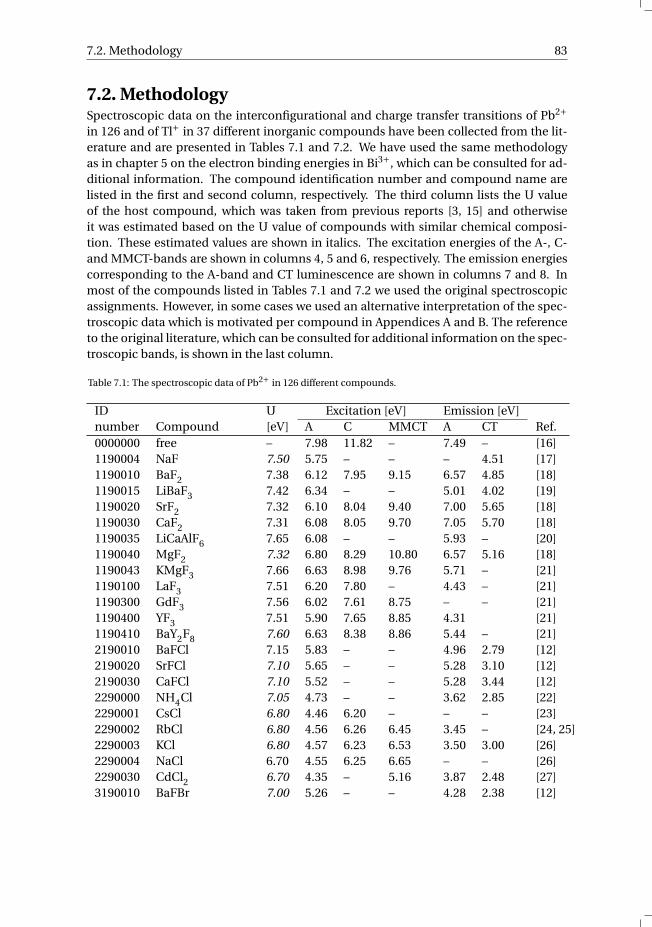
7.2. Methodology 83
7.2. MethodologySpectroscopic data on the interconfigurational and charge transfer transitions of Pb2+in 126 and of Tl+ in 37 different inorganic compounds have been collected from the lit-erature and are presented in Tables 7.1 and 7.2. We have used the same methodologyas in chapter 5 on the electron binding energies in Bi3+, which can be consulted for ad-ditional information. The compound identification number and compound name arelisted in the first and second column, respectively. The third column lists the U valueof the host compound, which was taken from previous reports [3, 15] and otherwiseit was estimated based on the U value of compounds with similar chemical composi-tion. These estimated values are shown in italics. The excitation energies of the A-, C-and MMCT-bands are shown in columns 4, 5 and 6, respectively. The emission energiescorresponding to the A-band and CT luminescence are shown in columns 7 and 8. Inmost of the compounds listed in Tables 7.1 and 7.2 we used the original spectroscopicassignments. However, in some cases we used an alternative interpretation of the spec-troscopic data which is motivated per compound in Appendices A and B. The referenceto the original literature, which can be consulted for additional information on the spec-troscopic bands, is shown in the last column.
Table 7.1: The spectroscopic data of Pb2+ in 126 different compounds.
ID U Excitation [eV] Emission [eV]number Compound [eV] A C MMCT A CT Ref.0000000 free – 7.98 11.82 – 7.49 – [16]1190004 NaF 7.50 5.75 – – – 4.51 [17]1190010 BaF2 7.38 6.12 7.95 9.15 6.57 4.85 [18]1190015 LiBaF3 7.42 6.34 – – 5.01 4.02 [19]1190020 SrF2 7.32 6.10 8.04 9.40 7.00 5.65 [18]1190030 CaF2 7.31 6.08 8.05 9.70 7.05 5.70 [18]1190035 LiCaAlF6 7.65 6.08 – – 5.93 – [20]1190040 MgF2 7.32 6.80 8.29 10.80 6.57 5.16 [18]1190043 KMgF3 7.66 6.63 8.98 9.76 5.71 – [21]1190100 LaF3 7.51 6.20 7.80 – 4.43 – [21]1190300 GdF3 7.56 6.02 7.61 8.75 – – [21]1190400 YF3 7.51 5.90 7.65 8.85 4.31 [21]1190410 BaY2F8 7.60 6.63 8.38 8.86 5.44 – [21]2190010 BaFCl 7.15 5.83 – – 4.96 2.79 [12]2190020 SrFCl 7.10 5.65 – – 5.28 3.10 [12]2190030 CaFCl 7.10 5.52 – – 5.28 3.44 [12]2290000 NH4Cl 7.05 4.73 – – 3.62 2.85 [22]2290001 CsCl 6.80 4.46 6.20 – – – [23]2290002 RbCl 6.80 4.56 6.26 6.45 3.45 – [24, 25]2290003 KCl 6.80 4.57 6.23 6.53 3.50 3.00 [26]2290004 NaCl 6.70 4.55 6.25 6.65 – – [26]2290030 CdCl2 6.70 4.35 – 5.16 3.87 2.48 [27]3190010 BaFBr 7.00 5.26 – – 4.28 2.38 [12]
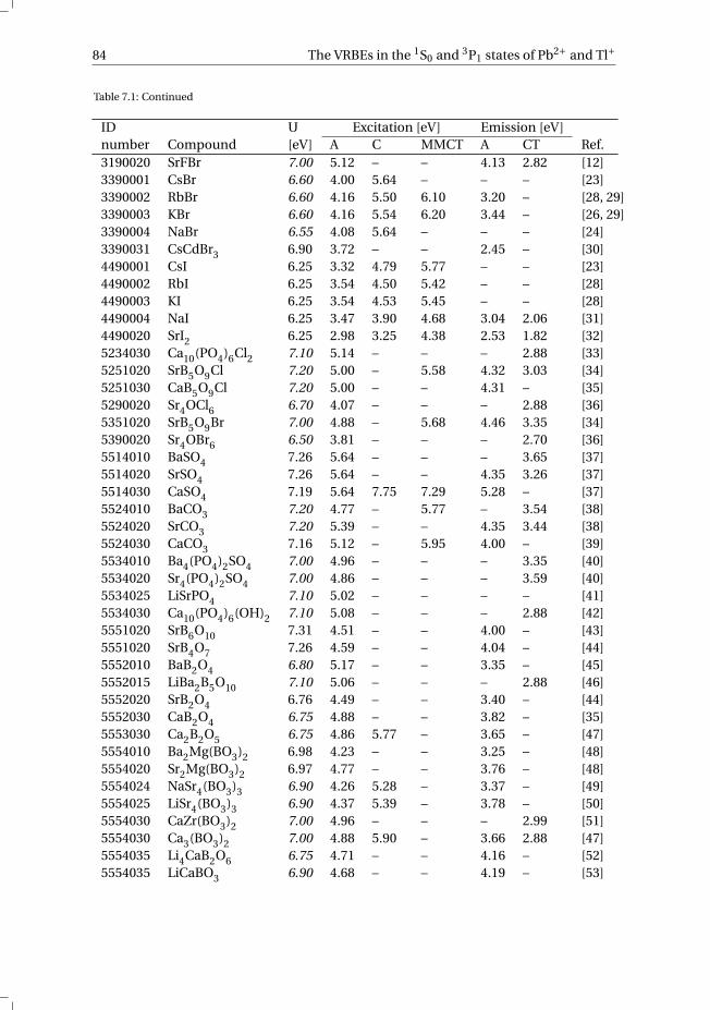
84 The VRBEs in the 1S0 and 3P1 states of Pb2+ and Tl+
Table 7.1: Continued
ID U Excitation [eV] Emission [eV]number Compound [eV] A C MMCT A CT Ref.3190020 SrFBr 7.00 5.12 – – 4.13 2.82 [12]3390001 CsBr 6.60 4.00 5.64 – – – [23]3390002 RbBr 6.60 4.16 5.50 6.10 3.20 – [28, 29]3390003 KBr 6.60 4.16 5.54 6.20 3.44 – [26, 29]3390004 NaBr 6.55 4.08 5.64 – – – [24]3390031 CsCdBr3 6.90 3.72 – – 2.45 – [30]4490001 CsI 6.25 3.32 4.79 5.77 – – [23]4490002 RbI 6.25 3.54 4.50 5.42 – – [28]4490003 KI 6.25 3.54 4.53 5.45 – – [28]4490004 NaI 6.25 3.47 3.90 4.68 3.04 2.06 [31]4490020 SrI2 6.25 2.98 3.25 4.38 2.53 1.82 [32]5234030 Ca10(PO4)6Cl2 7.10 5.14 – – – 2.88 [33]5251020 SrB5O9Cl 7.20 5.00 – 5.58 4.32 3.03 [34]5251030 CaB5O9Cl 7.20 5.00 – – 4.31 – [35]5290020 Sr4OCl6 6.70 4.07 – – – 2.88 [36]5351020 SrB5O9Br 7.00 4.88 – 5.68 4.46 3.35 [34]5390020 Sr4OBr6 6.50 3.81 – – – 2.70 [36]5514010 BaSO4 7.26 5.64 – – – 3.65 [37]5514020 SrSO4 7.26 5.64 – – 4.35 3.26 [37]5514030 CaSO4 7.19 5.64 7.75 7.29 5.28 – [37]5524010 BaCO3 7.20 4.77 – 5.77 – 3.54 [38]5524020 SrCO3 7.20 5.39 – – 4.35 3.44 [38]5524030 CaCO3 7.16 5.12 – 5.95 4.00 – [39]5534010 Ba4(PO4)2SO4 7.00 4.96 – – – 3.35 [40]5534020 Sr4(PO4)2SO4 7.00 4.86 – – – 3.59 [40]5534025 LiSrPO4 7.10 5.02 – – – – [41]5534030 Ca10(PO4)6(OH)2 7.10 5.08 – – – 2.88 [42]5551020 SrB6O10 7.31 4.51 – – 4.00 – [43]5551020 SrB4O7 7.26 4.59 – – 4.04 – [44]5552010 BaB2O4 6.80 5.17 – – 3.35 – [45]5552015 LiBa2B5O10 7.10 5.06 – – – 2.88 [46]5552020 SrB2O4 6.76 4.49 – – 3.40 – [44]5552030 CaB2O4 6.75 4.88 – – 3.82 – [35]5553030 Ca2B2O5 6.75 4.86 5.77 – 3.65 – [47]5554010 Ba2Mg(BO3)2 6.98 4.23 – – 3.25 – [48]5554020 Sr2Mg(BO3)2 6.97 4.77 – – 3.76 – [48]5554024 NaSr4(BO3)3 6.90 4.26 5.28 – 3.37 – [49]5554025 LiSr4(BO3)3 6.90 4.37 5.39 – 3.78 – [50]5554030 CaZr(BO3)2 7.00 4.96 – – – 2.99 [51]5554030 Ca3(BO3)2 7.00 4.88 5.90 – 3.66 2.88 [47]5554035 Li4CaB2O6 6.75 4.71 – – 4.16 – [52]5554035 LiCaBO3 6.90 4.68 – – 4.19 – [53]
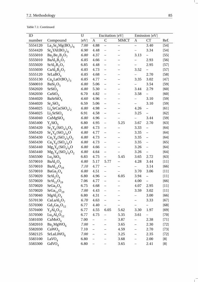
7.2. Methodology 85
Table 7.1: Continued
ID U Excitation [eV] Emission [eV]number Compound [eV] A C MMCT A CT Ref.5554120 La2Sr5Mg(BO3)6 7.00 4.88 – – – 3.40 [54]5554420 Sr6YAl(BO3)6 6.90 4.48 – – – 3.34 [54]5555010 Ba2Be2B2O7 6.80 4.37 – – 3.13 – [55]5555010 BaAl2B2O7 6.85 4.66 – – – 2.93 [56]5555020 SrAl2B2O7 6.85 4.48 – – – 2.95 [57]5555030 CaAl2B2O7 6.85 4.73 – – 3.52 – [57]5555120 SrLaBO4 6.85 4.68 – – – 2.70 [58]5555130 Ca4LaO(BO3)3 6.85 4.77 – – 3.35 3.02 [47]5560010 BaSi2O5 6.80 5.06 – – – 3.54 [59]5562020 SrSiO3 6.80 5.30 – – 3.44 2.79 [60]5562030 CaSiO3 6.70 4.82 – – 3.58 – [60]5564020 BaSrSiO4 6.60 4.96 – – – 3.10 [59]5564020 Sr2SiO4 6.59 5.06 – – – 3.10 [59]5564025 Li4SrCa(SiO4)2 6.80 4.98 – – 4.26 – [61]5564025 Li2SrSiO4 6.91 4.58 – – 3.25 – [62]5564040 CaMgSiO4 6.80 4.96 – – – 3.44 [59]5565400 Y2SiO5 6.80 4.95 – 5.25 3.67 2.70 [63]5565420 Sr2Y8(SiO4)6O2 6.80 4.73 – – 3.33 – [64]5565420 Sr4Y6(SiO4)6O 6.80 4.77 – – 3.35 – [64]5565430 Ca2Y8(SiO4)6O2 6.80 4.73 – – 3.35 – [64]5565430 Ca4Y6(SiO4)6O 6.80 4.73 – – 3.35 – [65]5565440 Mg4Y6(SiO4)6O 6.80 4.66 – – 3.26 – [64]5565440 Mg2Y8(SiO4)6O2 6.80 4.64 – – 3.26 – [64]5565500 Lu2SiO5 6.83 4.75 – 5.45 3.65 2.72 [63]5570010 BaAl2O4 6.80 5.17 5.77 – 4.28 3.44 [11]5570010 BaAl12O19 7.10 4.77 – – – 3.14 [66]5570010 BaGa2O4 6.80 4.51 – – 3.70 3.06 [11]5570020 SrAl2O4 6.80 4.96 – 6.05 3.94 – [11]5570020 SrAl12O19 7.06 4.77 – – 4.00 – [66]5570020 SrGa2O4 6.75 4.68 – – 4.07 2.95 [11]5570020 SrGa12O19 7.00 4.43 – – 3.59 3.02 [11]5570040 MgAl2O4 6.80 4.31 – – – 3.00 [66]5570130 CaLaAl3O7 6.70 4.63 – – – 3.33 [67]5570300 Gd3Ga5O12 6.77 4.40 – – – – [68]5570400 Y3Al5O12 6.77 4.55 6.05 5.62 3.30 1.97 [69]5570500 Lu3Al5O12 6.77 4.75 – 5.35 3.61 – [70]5581030 CaMoO4 7.00 – – 3.87 – 2.38 [71]5582010 Ba2MgWO6 7.00 – – 3.65 – 2.30 [72]5582030 CaWO4 7.10 – – 4.59 – 2.70 [73]5582125 SrLaLiWO6 7.00 – – 3.25 – 2.35 [72]5583100 LaVO4 6.80 – – 3.68 – 2.00 [8]5583300 GdVO4 6.80 – – 3.65 – 2.41 [8]
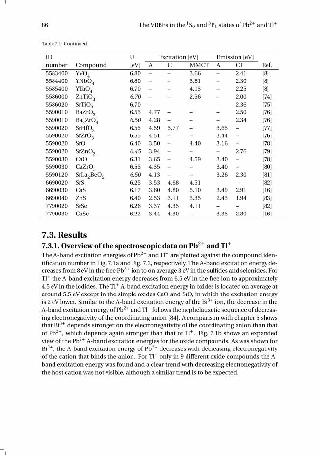
86 The VRBEs in the 1S0 and 3P1 states of Pb2+ and Tl+
Table 7.1: Continued
ID U Excitation [eV] Emission [eV]number Compound [eV] A C MMCT A CT Ref.5583400 YVO4 6.80 – – 3.66 – 2.41 [8]5584400 YNbO4 6.80 – – 3.81 – 2.30 [8]5585400 YTaO4 6.70 – – 4.13 – 2.25 [8]5586000 ZnTiO3 6.70 – – 2.56 – 2.00 [74]5586020 SrTiO3 6.70 – – – – 2.36 [75]5590010 BaZrO3 6.55 4.77 – – – 2.50 [76]5590010 Ba2ZrO4 6.50 4.28 – – – 2.34 [76]5590020 SrHfO3 6.55 4.59 5.77 – 3.65 – [77]5590020 SrZrO3 6.55 4.51 – – 3.44 – [76]5590020 SrO 6.40 3.50 – 4.40 3.16 – [78]5590020 SrZnO2 6.45 3.94 – – – 2.76 [79]5590030 CaO 6.31 3.65 – 4.59 3.40 – [78]5590030 CaZrO3 6.55 4.35 – – 3.40 – [80]5590120 SrLa2BeO5 6.50 4.13 – – 3.26 2.30 [81]6690020 SrS 6.25 3.53 4.68 4.51 – – [82]6690030 CaS 6.17 3.60 4.80 5.10 3.49 2.91 [16]6690040 ZnS 6.40 2.53 3.11 3.35 2.43 1.94 [83]7790020 SrSe 6.26 3.37 4.35 4.11 – – [82]7790030 CaSe 6.22 3.44 4.30 – 3.35 2.80 [16]
7.3. Results7.3.1. Overview of the spectroscopic data on Pb2+ and Tl+The A-band excitation energies of Pb2+ and Tl+ are plotted against the compound iden-tification number in Fig. 7.1a and Fig. 7.2, respectively. The A-band excitation energy de-creases from 8 eV in the free Pb2+ ion to on average 3 eV in the sulfides and selenides. ForTl+ the A-band excitation energy decreases from 6.5 eV in the free ion to approximately4.5 eV in the iodides. The Tl+ A-band excitation energy in oxides is located on average ataround 5.5 eV except in the simple oxides CaO and SrO, in which the excitation energyis 2 eV lower. Similar to the A-band excitation energy of the Bi3+ ion, the decrease in theA-band excitation energy of Pb2+ and Tl+ follows the nephelauxetic sequence of decreas-ing electronegativity of the coordinating anion [84]. A comparison with chapter 5 showsthat Bi3+ depends stronger on the electronegativity of the coordinating anion than thatof Pb2+, which depends again stronger than that of Tl+. Fig. 7.1b shows an expandedview of the Pb2+ A-band excitation energies for the oxide compounds. As was shown forBi3+, the A-band excitation energy of Pb2+ decreases with decreasing electronegativityof the cation that binds the anion. For Tl+ only in 9 different oxide compounds the A-band excitation energy was found and a clear trend with decreasing electronegativity ofthe host cation was not visible, although a similar trend is to be expected.
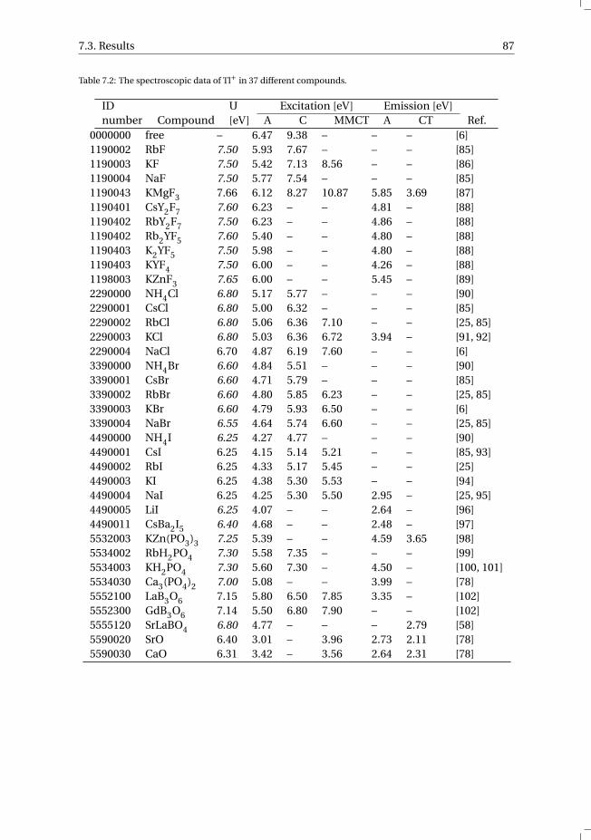
7.3. Results 87
Table 7.2: The spectroscopic data of Tl+ in 37 different compounds.
ID U Excitation [eV] Emission [eV]number Compound [eV] A C MMCT A CT Ref.
0000000 free – 6.47 9.38 – – – [6]1190002 RbF 7.50 5.93 7.67 – – – [85]1190003 KF 7.50 5.42 7.13 8.56 – – [86]1190004 NaF 7.50 5.77 7.54 – – – [85]1190043 KMgF3 7.66 6.12 8.27 10.87 5.85 3.69 [87]1190401 CsY2F7 7.60 6.23 – – 4.81 – [88]1190402 RbY2F7 7.50 6.23 – – 4.86 – [88]1190402 Rb2YF5 7.60 5.40 – – 4.80 – [88]1190403 K2YF5 7.50 5.98 – – 4.80 – [88]1190403 KYF4 7.50 6.00 – – 4.26 – [88]1198003 KZnF3 7.65 6.00 – – 5.45 – [89]2290000 NH4Cl 6.80 5.17 5.77 – – – [90]2290001 CsCl 6.80 5.00 6.32 – – – [85]2290002 RbCl 6.80 5.06 6.36 7.10 – – [25, 85]2290003 KCl 6.80 5.03 6.36 6.72 3.94 – [91, 92]2290004 NaCl 6.70 4.87 6.19 7.60 – – [6]3390000 NH4Br 6.60 4.84 5.51 – – – [90]3390001 CsBr 6.60 4.71 5.79 – – – [85]3390002 RbBr 6.60 4.80 5.85 6.23 – – [25, 85]3390003 KBr 6.60 4.79 5.93 6.50 – – [6]3390004 NaBr 6.55 4.64 5.74 6.60 – – [25, 85]4490000 NH4I 6.25 4.27 4.77 – – – [90]4490001 CsI 6.25 4.15 5.14 5.21 – – [85, 93]4490002 RbI 6.25 4.33 5.17 5.45 – – [25]4490003 KI 6.25 4.38 5.30 5.53 – – [94]4490004 NaI 6.25 4.25 5.30 5.50 2.95 – [25, 95]4490005 LiI 6.25 4.07 – – 2.64 – [96]4490011 CsBa2I5 6.40 4.68 – – 2.48 – [97]5532003 KZn(PO3)3 7.25 5.39 – – 4.59 3.65 [98]5534002 RbH2PO4 7.30 5.58 7.35 – – – [99]5534003 KH2PO4 7.30 5.60 7.30 – 4.50 – [100, 101]5534030 Ca3(PO4)2 7.00 5.08 – – 3.99 – [78]5552100 LaB3O6 7.15 5.80 6.50 7.85 3.35 – [102]5552300 GdB3O6 7.14 5.50 6.80 7.90 – – [102]5555120 SrLaBO4 6.80 4.77 – – – 2.79 [58]5590020 SrO 6.40 3.01 – 3.96 2.73 2.11 [78]5590030 CaO 6.31 3.42 – 3.56 2.64 2.31 [78]
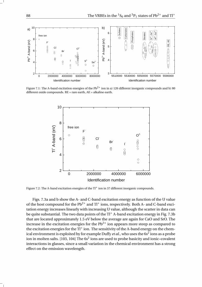
88 The VRBEs in the 1S0 and 3P1 states of Pb2+ and Tl+
0 2 0 0 0 0 0 0 4 0 0 0 0 0 0 6 0 0 0 0 0 0 8 0 0 0 0 0 02
4
6
8
1 0a )Pb
2+ A-
band
(eV)
I d e n t i f i c a t i o n n u m b e r
f r e e i o n
F -
C l -B r -
I -
O 2 -
S 2 - S e 2 -
5 5 1 0 0 0 0 5 5 3 0 0 0 0 5 5 5 0 0 0 0 5 5 7 0 0 0 0 5 5 9 0 0 0 03
4
5
6b )
Carbo
nates
Pb2+
A-ba
nd (e
V)
I d e n t i f i c a t i o n n u m b e r
Phos
phate
s
Borat
es
Si4+, G
e4+
Al3+, G
a3+
RE, A
E
Sulfa
tes
Figure 7.1: The A-band excitation energies of the Pb2+ ion in a) 126 different inorganic compounds and b) 80different oxide compounds. RE = rare earth, AE = alkaline earth.
0 2 0 0 0 0 0 0 4 0 0 0 0 0 0 6 0 0 0 0 0 02
4
6
8
1 0
Tl+ A-ba
nd (e
V)
I d e n t i f i c a t i o n n u m b e r
f r e e i o nF -
C l - B r -I -
O 2 -
Figure 7.2: The A-band excitation energies of the Tl+ ion in 37 different inorganic compounds.
Figs. 7.3a and b show the A- and C-band excitation energy as function of the U valueof the host compound for the Pb2+ and Tl+ ions, respectively. Both A- and C-band exci-tation energy increases linearly with increasing U value, although the scatter in data canbe quite substantial. The two data points of the Tl+ A-band excitation energy in Fig. 7.3bthat are located approximately 1.5 eV below the average are again for CaO and SrO. Theincrease in the excitation energies for the Pb2+ ion appears more steep as compared tothe excitation energies for the Tl+ ion. The sensitivity of the A-band energy on the chem-ical environment is exploited by for example Duffy et al., who uses the 6s2 ions as a probeion in molten salts. [103, 104] The 6s2 ions are used to probe basicity and ionic–covalentinteractions in glasses, since a small variation in the chemical environment has a strongeffect on the emission wavelength.
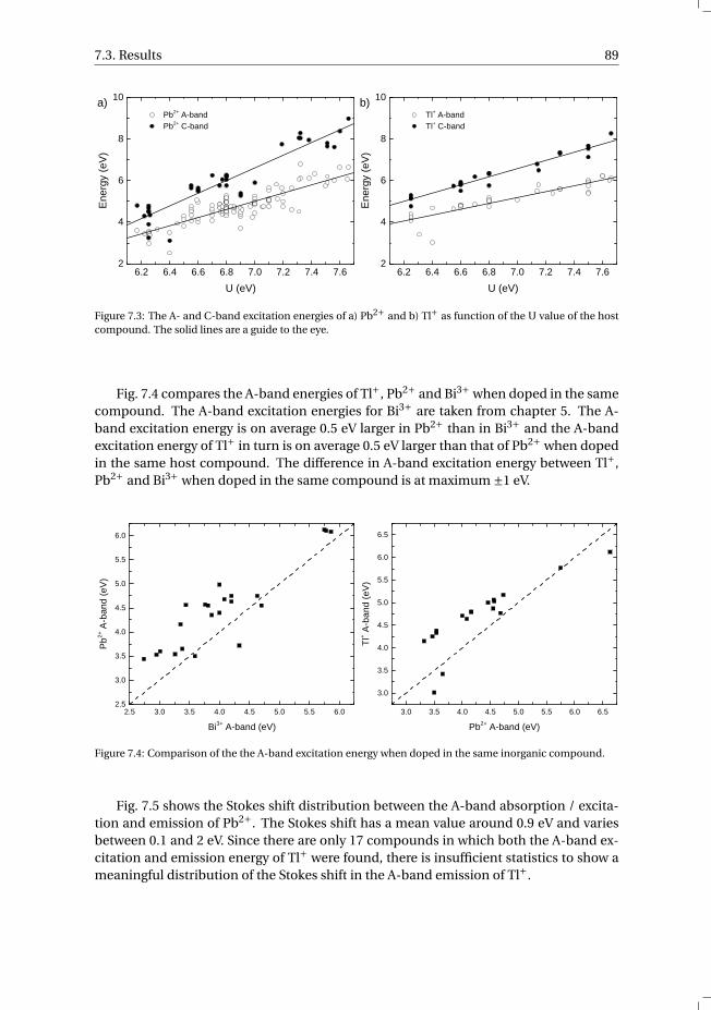
7.3. Results 89
6 . 2 6 . 4 6 . 6 6 . 8 7 . 0 7 . 2 7 . 4 7 . 62
4
6
8
1 0a ) P b 2 + A - b a n d P b 2 + C - b a n d
Energ
y (eV
)
U ( e V )6 . 2 6 . 4 6 . 6 6 . 8 7 . 0 7 . 2 7 . 4 7 . 62
4
6
8
1 0b ) T l + A - b a n d T l + C - b a n d
Energ
y (eV
)
U ( e V )
Figure 7.3: The A- and C-band excitation energies of a) Pb2+ and b) Tl+ as function of the U value of the hostcompound. The solid lines are a guide to the eye.
Fig. 7.4 compares the A-band energies of Tl+, Pb2+ and Bi3+ when doped in the samecompound. The A-band excitation energies for Bi3+ are taken from chapter 5. The A-band excitation energy is on average 0.5 eV larger in Pb2+ than in Bi3+ and the A-bandexcitation energy of Tl+ in turn is on average 0.5 eV larger than that of Pb2+ when dopedin the same host compound. The difference in A-band excitation energy between Tl+,Pb2+ and Bi3+ when doped in the same compound is at maximum ±1 eV.
2 . 5 3 . 0 3 . 5 4 . 0 4 . 5 5 . 0 5 . 5 6 . 02 . 5
3 . 0
3 . 5
4 . 0
4 . 5
5 . 0
5 . 5
6 . 0
Pb2+
A-ba
nd (e
V)
B i 3 + A - b a n d ( e V )3 . 0 3 . 5 4 . 0 4 . 5 5 . 0 5 . 5 6 . 0 6 . 5
3 . 0
3 . 5
4 . 0
4 . 5
5 . 0
5 . 5
6 . 0
6 . 5
Tl+ A-ba
nd (e
V)
P b 2 + A - b a n d ( e V )
Figure 7.4: Comparison of the the A-band excitation energy when doped in the same inorganic compound.
Fig. 7.5 shows the Stokes shift distribution between the A-band absorption / excita-tion and emission of Pb2+. The Stokes shift has a mean value around 0.9 eV and variesbetween 0.1 and 2 eV. Since there are only 17 compounds in which both the A-band ex-citation and emission energy of Tl+ were found, there is insufficient statistics to show ameaningful distribution of the Stokes shift in the A-band emission of Tl+.
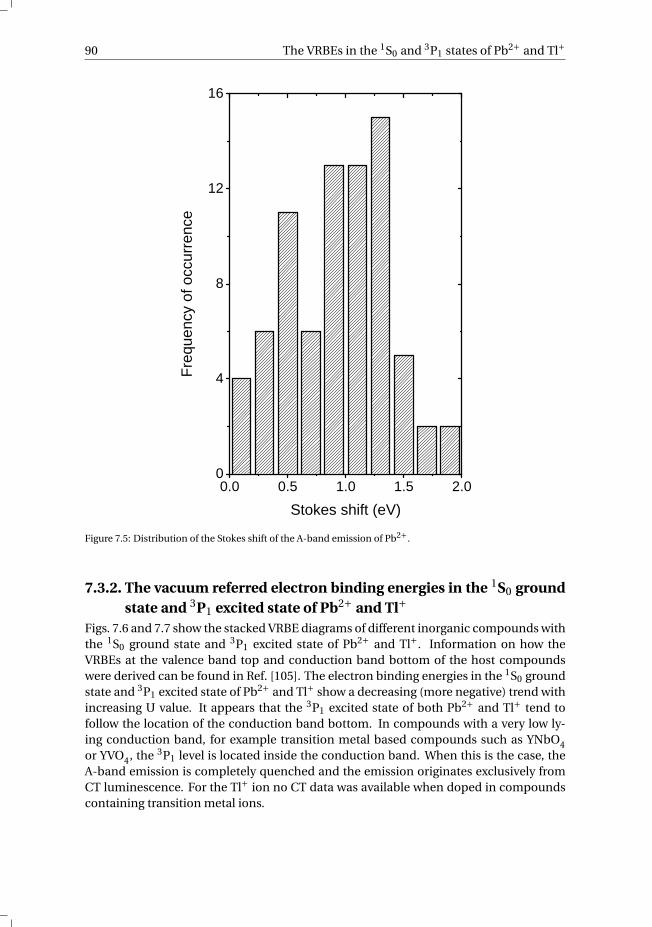
90 The VRBEs in the 1S0 and 3P1 states of Pb2+ and Tl+
0 . 0 0 . 5 1 . 0 1 . 5 2 . 00
4
8
1 2
1 6
Frequ
ency
of oc
curre
nce
S t o k e s s h i f t ( e V )Figure 7.5: Distribution of the Stokes shift of the A-band emission of Pb2+.
7.3.2. The vacuum referred electron binding energies in the 1S0 groundstate and 3P1 excited state of Pb2+ and Tl+
Figs. 7.6 and 7.7 show the stacked VRBE diagrams of different inorganic compounds withthe 1S0 ground state and 3P1 excited state of Pb2+ and Tl+. Information on how theVRBEs at the valence band top and conduction band bottom of the host compoundswere derived can be found in Ref. [105]. The electron binding energies in the 1S0 groundstate and 3P1 excited state of Pb2+ and Tl+ show a decreasing (more negative) trend withincreasing U value. It appears that the 3P1 excited state of both Pb2+ and Tl+ tend tofollow the location of the conduction band bottom. In compounds with a very low ly-ing conduction band, for example transition metal based compounds such as YNbO4or YVO4, the 3P1 level is located inside the conduction band. When this is the case, theA-band emission is completely quenched and the emission originates exclusively fromCT luminescence. For the Tl+ ion no CT data was available when doped in compoundscontaining transition metal ions.
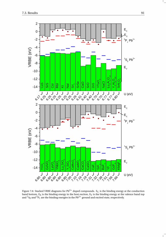
7.3. Results 91
- 1 4- 1 2- 1 0
- 8- 6- 4- 202
E V
6 . 2 5
KIRbI
CsI
SrS
VRBE
(eV)
CaS
1 S 0 P b 2 +
3 P 1 P b 2 +E X
U ( e V )
E C
SrOCaO
SrSe
NaI
SrI2
ZnS
YTaO
4Na
ClLu
3Al5O
12Y 3Al
5O12
SrAl 2O 4
6 . 2 56 . 2 56 . 1 7 6 . 2 56 . 2 5 6 . 4 06 . 2 5 6 . 3 16 . 2 6 6 . 4 0 6 . 7 0 6 . 7 0 6 . 8 06 . 7 76 . 7 7
- 1 4- 1 2- 1 0
- 8- 6- 4- 202
GdF 3 E V
6 . 8 0
Lu2Si
O 5
YNbO
4
LaVO
4
GdVO
4
VRBE
(eV)
YVO 4
1 S 0 P b 2 +
3 P 1 P b 2 +
E X
U ( e V )
E C
CaSO
4
CaCO
3
CaWO
4
Y 2SiO 5
CaMo
O 4
CaF 2
SrF2
BaF 2
YF3
KMgF
3
6 . 8 06 . 8 06 . 8 0 6 . 8 06 . 8 0 7 . 1 97 . 0 0 7 . 1 67 . 1 0 7 . 3 1 7 . 3 2 7 . 3 8 7 . 6 67 . 5 67 . 5 1
Figure 7.6: Stacked VRBE diagrams for Pb2+ doped compounds. EC is the binding energy at the conductionband bottom, EX is the binding energy in the host exciton, EV is the binding energy at the valence band topand 1S0 and 3P1 are the binding energies in the Pb2+ ground and excited state, respectively.
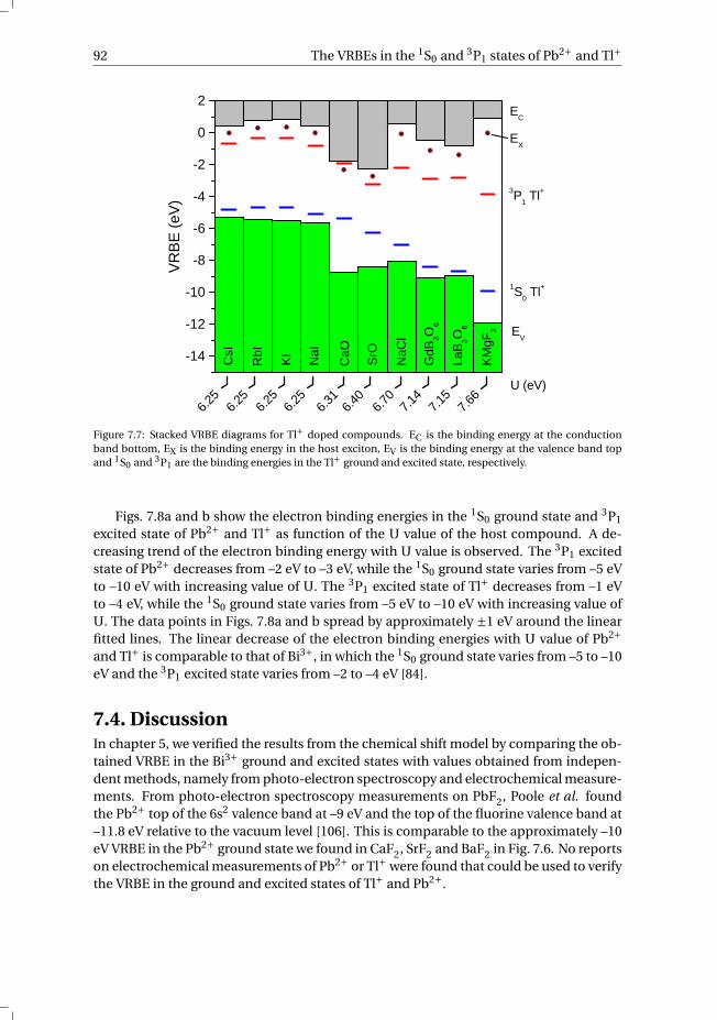
92 The VRBEs in the 1S0 and 3P1 states of Pb2+ and Tl+
- 1 4- 1 2- 1 0
- 8- 6- 4- 202
KMgF
3
LaB 3O
6
GdB 3O
6
NaCl
SrO
VRBE
(eV)
CaO
1 S 0 T l +
3 P 1 T l +
E X
E V
E C
6 . 3 1U ( e V )
6 . 2 56 . 2 5 6 . 2 56 . 2 5 7 . 1 56 . 4 0 7 . 1 46 . 7 0 7 . 6 6
NaI
KIRbI
CsI
Figure 7.7: Stacked VRBE diagrams for Tl+ doped compounds. EC is the binding energy at the conductionband bottom, EX is the binding energy in the host exciton, EV is the binding energy at the valence band topand 1S0 and 3P1 are the binding energies in the Tl+ ground and excited state, respectively.
Figs. 7.8a and b show the electron binding energies in the 1S0 ground state and 3P1
excited state of Pb2+ and Tl+ as function of the U value of the host compound. A de-creasing trend of the electron binding energy with U value is observed. The 3P1 excitedstate of Pb2+ decreases from –2 eV to –3 eV, while the 1S0 ground state varies from –5 eVto –10 eV with increasing value of U. The 3P1 excited state of Tl+ decreases from –1 eVto –4 eV, while the 1S0 ground state varies from –5 eV to –10 eV with increasing value ofU. The data points in Figs. 7.8a and b spread by approximately ±1 eV around the linearfitted lines. The linear decrease of the electron binding energies with U value of Pb2+and Tl+ is comparable to that of Bi3+, in which the 1S0 ground state varies from –5 to –10eV and the 3P1 excited state varies from –2 to –4 eV [84].
7.4. DiscussionIn chapter 5, we verified the results from the chemical shift model by comparing the ob-tained VRBE in the Bi3+ ground and excited states with values obtained from indepen-dent methods, namely from photo-electron spectroscopy and electrochemical measure-ments. From photo-electron spectroscopy measurements on PbF2, Poole et al. foundthe Pb2+ top of the 6s2 valence band at –9 eV and the top of the fluorine valence band at–11.8 eV relative to the vacuum level [106]. This is comparable to the approximately –10eV VRBE in the Pb2+ ground state we found in CaF2, SrF2 and BaF2 in Fig. 7.6. No reportson electrochemical measurements of Pb2+ or Tl+ were found that could be used to verifythe VRBE in the ground and excited states of Tl+ and Pb2+.
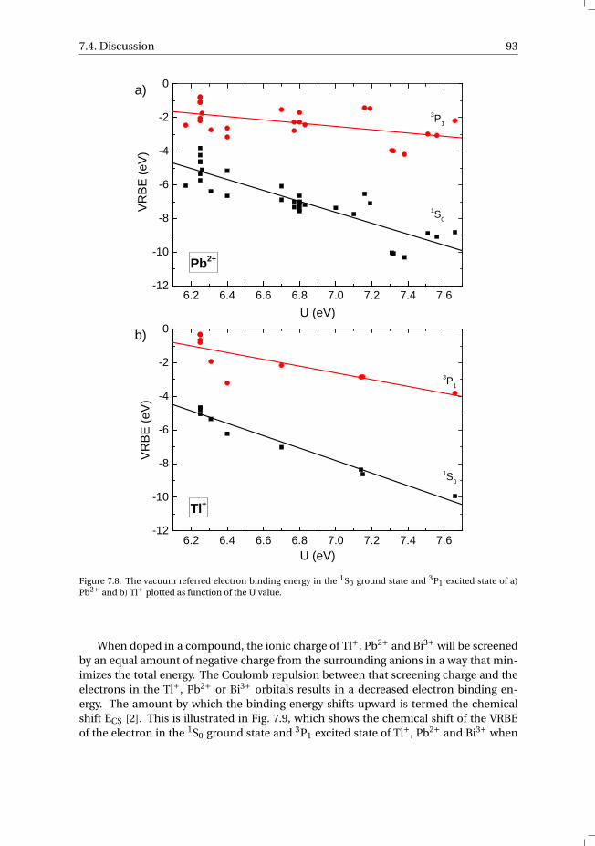
7.4. Discussion 93
6 . 2 6 . 4 6 . 6 6 . 8 7 . 0 7 . 2 7 . 4 7 . 6- 1 2
- 1 0
- 8
- 6
- 4
- 2
0
P b 2 +
a )
VRBE
(eV)
U ( e V )
1 S 0
3 P 1
6 . 2 6 . 4 6 . 6 6 . 8 7 . 0 7 . 2 7 . 4 7 . 6- 1 2
- 1 0
- 8
- 6
- 4
- 2
0b )
VRBE
(eV)
U ( e V )
1 S 0
3 P 1
T l +
Figure 7.8: The vacuum referred electron binding energy in the 1S0 ground state and 3P1 excited state of a)Pb2+ and b) Tl+ plotted as function of the U value.
When doped in a compound, the ionic charge of Tl+, Pb2+ and Bi3+ will be screenedby an equal amount of negative charge from the surrounding anions in a way that min-imizes the total energy. The Coulomb repulsion between that screening charge and theelectrons in the Tl+, Pb2+ or Bi3+ orbitals results in a decreased electron binding en-ergy. The amount by which the binding energy shifts upward is termed the chemicalshift ECS [2]. This is illustrated in Fig. 7.9, which shows the chemical shift of the VRBEof the electron in the 1S0 ground state and 3P1 excited state of Tl+, Pb2+ and Bi3+ when
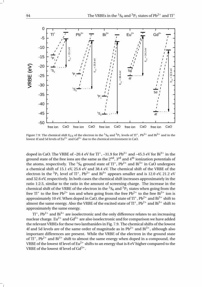
94 The VRBEs in the 1S0 and 3P1 states of Pb2+ and Tl+
- 5 0- 4 5- 4 0- 3 5- 3 0- 2 5- 2 0- 1 5- 1 0
- 50
5 d
5 d
4 f
4 f
VRBE
(eV)
E CS
= 38
.4 eVE CS
= 25
.6 eV
B i 3 +P b 2 +VR
BE (e
V)
f r e e i o n C a O
E CS =
15.1
eV
T l +
1 S 0
3 P 1
f r e e i o n C a O f r e e i o n C a O
3 P 1
1 S 03 P 1
1 S 0
f r e e i o n C a O f r e e i o n C a O
E u 2 + G d 3 +
E CS =
32.6
eV
E CS =
24.2
eV
Figure 7.9: The chemical shift ECS of the electron in the 1S0 and 3P1 levels of Tl+, Pb2+ and Bi3+ and in thelowest 4f and 5d levels of Eu2+ and Gd3+ due to the chemical environment in CaO.
doped in CaO. The VRBE of –20.4 eV for Tl+, –31.9 for Pb2+ and –45.3 eV for Bi3+ in theground state of the free ions are the same as the 2nd, 3rd and 4th ionization potentials ofthe atoms, respectively. The 1S0 ground state of Tl+, Pb2+ and Bi3+ in CaO undergoesa chemical shift of 15.1 eV, 25.6 eV and 38.4 eV. The chemical shift of the VRBE of theelectron in the 3P1 level of Tl+, Pb2+ and Bi3+ appears smaller and is 12.0 eV, 21.2 eVand 32.6 eV, respectively. In both cases the chemical shift increases approximately in theratio 1:2:3, similar to the ratio in the amount of screening charge. The increase in thechemical shift of the VRBE of the electron in the 1S0 and 3P1 states when going from thefree Tl+ to the free Pb2+ ion and when going from the free Pb2+ to the free Bi3+ ion isapproximately 10 eV. When doped in CaO, the ground state of Tl+, Pb2+ and Bi3+ shift toalmost the same energy. Also the VRBE of the excited state of Tl+, Pb2+ and Bi3+ shift toapproximately the same energy.
Tl+, Pb2+ and Bi3+ are isoelectronic and the only difference relates to an increasingnuclear charge. Eu2+ and Gd3+ are also isoelectronic and for comparison we have addedthe relevant VRBEs for these two lanthanides in Fig. 7.9. The chemical shifts of the lowest4f and 5d levels are of the same order of magnitude as in Pb2+ and Bi3+, although alsoimportant differences are present. While the VRBE of the electron in the ground stateof Tl+, Pb2+ and Bi3+ shift to almost the same energy when doped in a compound, theVRBE of the lowest 4f level of Eu2+ shifts to an energy that is 8 eV higher compared to theVRBE of the lowest 4f level of Gd3+.
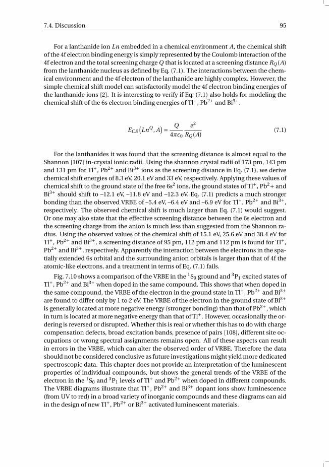
7.4. Discussion 95
For a lanthanide ion Ln embedded in a chemical environment A, the chemical shiftof the 4f electron binding energy is simply represented by the Coulomb interaction of the4f electron and the total screening charge Q that is located at a screening distance RQ (A)from the lanthanide nucleus as defined by Eq. (7.1). The interactions between the chem-ical environment and the 4f electron of the lanthanide are highly complex. However, thesimple chemical shift model can satisfactorily model the 4f electron binding energies ofthe lanthanide ions [2]. It is interesting to verify if Eq. (7.1) also holds for modeling thechemical shift of the 6s electron binding energies of Tl+, Pb2+ and Bi3+.
EC S(LnQ , A
)= Q
4πε0
e2
RQ (A)(7.1)
For the lanthanides it was found that the screening distance is almost equal to theShannon [107] in-crystal ionic radii. Using the shannon crystal radii of 173 pm, 143 pmand 131 pm for Tl+, Pb2+ and Bi3+ ions as the screening distance in Eq. (7.1), we derivechemical shift energies of 8.3 eV, 20.1 eV and 33 eV, respectively. Applying these values ofchemical shift to the ground state of the free 6s2 ions, the ground states of Tl+, Pb2+ andBi3+ should shift to –12.1 eV, –11.8 eV and –12.3 eV. Eq. (7.1) predicts a much strongerbonding than the observed VRBE of –5.4 eV, –6.4 eV and –6.9 eV for Tl+, Pb2+ and Bi3+,respectively. The observed chemical shift is much larger than Eq. (7.1) would suggest.Or one may also state that the effective screening distance between the 6s electron andthe screening charge from the anion is much less than suggested from the Shannon ra-dius. Using the observed values of the chemical shift of 15.1 eV, 25.6 eV and 38.4 eV forTl+, Pb2+ and Bi3+, a screening distance of 95 pm, 112 pm and 112 pm is found for Tl+,Pb2+ and Bi3+, respectively. Apparently the interaction between the electrons in the spa-tially extended 6s orbital and the surrounding anion orbitals is larger than that of 4f theatomic-like electrons, and a treatment in terms of Eq. (7.1) fails.
Fig. 7.10 shows a comparison of the VRBE in the 1S0 ground and 3P1 excited states ofTl+, Pb2+ and Bi3+ when doped in the same compound. This shows that when doped inthe same compound, the VRBE of the electron in the ground state in Tl+, Pb2+ and Bi3+are found to differ only by 1 to 2 eV. The VRBE of the electron in the ground state of Bi3+is generally located at more negative energy (stronger bonding) than that of Pb2+, whichin turn is located at more negative energy than that of Tl+. However, occasionally the or-dering is reversed or disrupted. Whether this is real or whether this has to do with chargecompensation defects, broad excitation bands, presence of pairs [108], different site oc-cupations or wrong spectral assignments remains open. All of these aspects can resultin errors in the VRBE, which can alter the observed order of VRBE. Therefore the datashould not be considered conclusive as future investigations might yield more dedicatedspectroscopic data. This chapter does not provide an interpretation of the luminescentproperties of individual compounds, but shows the general trends of the VRBE of theelectron in the 1S0 and 3P1 levels of Tl+ and Pb2+ when doped in different compounds.The VRBE diagrams illustrate that Tl+, Pb2+ and Bi3+ dopant ions show luminescence(from UV to red) in a broad variety of inorganic compounds and these diagrams can aidin the design of new Tl+, Pb2+ or Bi3+ activated luminescent materials.
96 The VRBEs in the 1S0 and 3P1 states of Pb2+ and Tl+
CaS CsI
RbI KI NaI
CaO SrO NaCl
YTaO
4Y 3Al
5O12
Lu3Al
5O12
YNbO
4YV
O 4Gd
VO4
LaVO
4Ca
MoO 4
CaWO
4Ca
F 2SrF
2Ba
F 2KM
gF3- 1 1
- 1 0
- 9
- 8
- 7
- 6
- 5
- 4a )
T l + P b 2 +
B i 3 +
VRBE
1 S 0
CaS CsI
RbI KI NaI
CaO SrO NaCl
YTaO
4Y 3Al
5O12
Lu3Al
5O12
CaF 2
SrF2
BaF 2
KMgF
3- 6
- 5
- 4
- 3
- 2
- 1
0
T l + P b 2 +
B i 3 +
VRBE
3 P 1
b )
C e 5 d
Figure 7.10: Comparison of the vacuum referred electron binding energy in the a) 1S0 and b) 3P1 levels of Tl+,Pb2+ and Bi3+ when doped in the same inorganic compounds.
7.5. Summary and conclusions 97
Considering the large compound to compound variation in the 6s and 6p electronVRBE, it not yet possible to predict exactly which Tl-, Pb- or Bi-based compounds wouldshow efficient Ce3+ luminescence. The lowest 5d electron VRBE of Ce3+ is located on av-erage at –1.8 eV with ±0.5 eV compound to compound variation [109], which is markedby the shaded region in Fig. 7.10b. In order for Ce3+ to show efficient luminescence, theVRBE at the CB bottom should be at higher energy than the VRBE of the 5d electron ofCe3+, i.e. higher than –1.8 eV. The VRBE of the electron in the 3P1 excited state generallydecreases in going from Tl+ to Pb2+ to Bi3+ and varies between –1 eV and –4 eV depend-ing on the U value of the host. The conduction band bottom in Tl-, Pb- and Bi-basedcompounds will be determined by the VRBE of the electron in the ground state of Tl0,Pb+ and Bi2+. In chapter 6 we showed that the VRBE in the ground state of Bi2+ is lo-cated close to or slightly deeper than the VRBE in the 3P1 excited state of Bi3+. Assumingthat the ground state in Tl0 and Pb+ ions are also located close to or slightly above the3P1 level of Tl+ and Pb2+, the results suggest that the highest probability to achieve effi-cient Ce3+ luminescence is in Tl- or Pb-based iodide compounds. Since the ground andexcited state of Tl+ are found to be at the highest VRBE (least negative VRBE) of the 6s2
ions and efficient Ce3+ luminescence is already reported in Tl-based halide crystals [110–112], Tl-based halide compounds show the most potential as Ce3+ activated scintillatormaterials. Unfortunately, it is not possible to achieve high densities (>8 g/cm3) for halidecompounds.
7.5. Summary and conclusionsSpectroscopic data on the metal-to-metal charge transfer and interconfigurational tran-sitions of the Tl+ and Pb2+ activator ions in 37 and 126 different inorganic compounds,respectively, were gathered from the available literature. The MMCT energy was used todetermine the vacuum referred electron binding energy in the 1S0 ground state of Tl+and Pb2+ in 10 and 32 different host compounds. By adding the A-band energy, the elec-tron binding energy in the 3P1 excited state of Tl+ and Pb2+ was obtained. The VRBE ofthe electron in the 1S0 ground state and 3P1 excited state of Tl+ and Pb2+ were found tolinearly decrease with U value and follow the nephelauxetic sequence. When doped inCaO, the 1S0 ground state of Tl+, Pb2+ and Bi3+ was found to be subjected to a chemi-cal shift of 15.1 eV, 25.6 eV and 38.4 eV for Tl+, Pb2+ and Bi3+, while the chemical shiftof the VRBE of the electron in the 3P1 level of Tl+, Pb2+ and Bi3+ appeared smaller andwas found to be 12.0 eV, 21.2 eV and 32.6 eV, respectively. In both cases the chemicalshift was found to increase approximately in the ratio 1:2:3, similar to the ratio in theamount of screening charge. When doped in a compound, the ground state of Tl+, Pb2+and Bi3+ were found to shift to almost the same energy. It was found that the simplechemical shift model that can satisfactorily model the 4f electron binding energies ofthe lanthanide ions, does not apply to the 6s electron binding energies. Apparently theinteraction between the electrons in the spatially extended 6s orbital and the surround-ing anion orbitals is larger than that of 4f the atomic-like electrons. Based on the deter-mined VRBEs of the electron in 1S0 and 3P1 states, Tl-based compounds (mainly iodides)showed the most potential for Ce3+ activated scintillator materials.
98 The VRBEs in the 1S0 and 3P1 states of Pb2+ and Tl+
AppendicesIn most of the literature we reviewed, the MMCT transition is labeled as D-band. Insome of the compounds however, our interpretation deviated from the originally as-signed transitions. In Appendices A and B we justify our interpretation and tentativeassignments of the spectroscopic data of the Pb2+ and Tl+ ions in the reported literaturedata. The assignment of the interconfigurational A- and C-band transition are ratherstraightforward and therefore we limit ourselves to discussing only the MMCT transi-tions and refer to the original literature for more information.
7.6. Appendix A. The metal-to-metal charge transfer ener-gies of Pb2+
SrI2 Chen et al. studied single crystals of SrI2:Pb2+ [32]. They assigned the 3.25, 3.72 and4.38 eV excitation bands to the A-, B- and C-bands, respectively. However, we suggestthat the 2.98 eV, 3.25 eV and 4.38 eV transitions should be attributed to the A-, C- andMMCT-bands, respectively. Due to the forbidden nature of the B-band it should be veryweak in photoluminescence spectra. Furthermore, the lowest energy excitation band at2.98 eV should be assigned to the A-band. The most intense excitation band at 3.25 eV webelieve is from the allowed C-band transition. The high-energy of the 4.38 eV transition,indicates this is the MMCT transition band.SrB5O9Cl Meijerink et al. reported a dominant excitation band at 5.58 eV for Pb2+-dopedSr2B5O9Cl, which they assigned to the C-band. [34] However, they mentioned that itcould not be excluded that the C-band (partly) overlapped with a charge transfer transi-tion. Therefore, we assigned the 5.58 eV to the MMCT transition, taken into account thatthere is probably an error in the exact energy of the MMCT transition due to the overlapwith the C-band.SrB5O9Br Similar to SrB5O9Cl, Meijerink et al. reported a dominant excitation band at5.68 eV for Sr1.9B5O9Br:Pb0.1, which they assigned to the C-band [34]. However, theymentioned that it could not be excluded that the C-band (partly) overlapped with acharge transfer transition. Therefore, we assigned the 5.68 eV to the MMCT transition,taken into account that there is probably an error in the exact energy of the MMCT tran-sition due to the overlap with the C-band.CaCO3 Kraienhemke et al. recognized a weak band close to the fundamental absorptionedge but did not assign this band to a transition [39]. Due to the high energy of the 5.95eV band, we attribute this band to the MMCT transition.Y2SiO5 and Lu2SiO5 Babin et al. observed excitation bands at 4.95 eV and 5.25 eV forY2SiO5, which they assigned to A-band emission of Pb2+ on a different crystallographicsites [63]. However, the 5.25 eV excitation and corresponding emission at 2.7 eV, showeda concentration dependence typical for the MMCT transition. This lead us to suggestthat this transition is more likely from the MMCT transition. In the same report, Babinet al. reported excitation at 5.45 eV Lu2SiO5, which we tentatively assigned to the MMCTtransition instead of excitation of Pb2+ on a different crystallographic site.Lu3Al5O12 Babin et al. reported the A-band excitation and emission at 4.75 eV and 3.61eV, respectively [70]. Another excitation at 5.35 eV was observed which they related to adifferent but undefined origin, which we assigned to the MMCT transition.
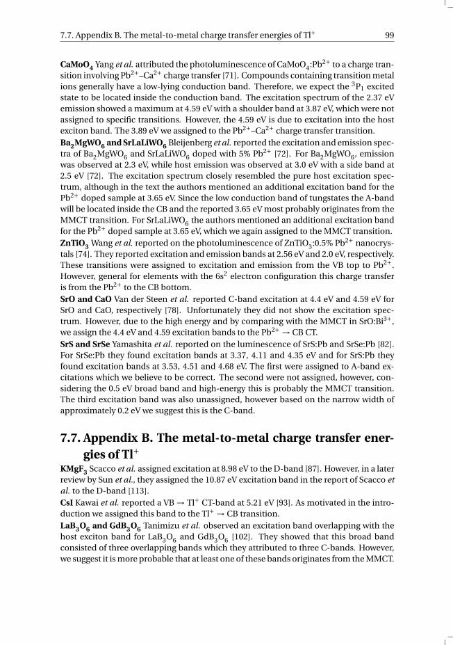
7.7. Appendix B. The metal-to-metal charge transfer energies of Tl+ 99
CaMoO4 Yang et al. attributed the photoluminescence of CaMoO4:Pb2+ to a charge tran-sition involving Pb2+–Ca2+ charge transfer [71]. Compounds containing transition metalions generally have a low-lying conduction band. Therefore, we expect the 3P1 excitedstate to be located inside the conduction band. The excitation spectrum of the 2.37 eVemission showed a maximum at 4.59 eV with a shoulder band at 3.87 eV, which were notassigned to specific transitions. However, the 4.59 eV is due to excitation into the hostexciton band. The 3.89 eV we assigned to the Pb2+–Ca2+ charge transfer transition.Ba2MgWO6 and SrLaLiWO6 Bleijenberg et al. reported the excitation and emission spec-tra of Ba2MgWO6 and SrLaLiWO6 doped with 5% Pb2+ [72]. For Ba2MgWO6, emissionwas observed at 2.3 eV, while host emission was observed at 3.0 eV with a side band at2.5 eV [72]. The excitation spectrum closely resembled the pure host excitation spec-trum, although in the text the authors mentioned an additional excitation band for thePb2+ doped sample at 3.65 eV. Since the low conduction band of tungstates the A-bandwill be located inside the CB and the reported 3.65 eV most probably originates from theMMCT transition. For SrLaLiWO6 the authors mentioned an additional excitation bandfor the Pb2+ doped sample at 3.65 eV, which we again assigned to the MMCT transition.ZnTiO3 Wang et al. reported on the photoluminescence of ZnTiO3:0.5% Pb2+ nanocrys-tals [74]. They reported excitation and emission bands at 2.56 eV and 2.0 eV, respectively.These transitions were assigned to excitation and emission from the VB top to Pb2+.However, general for elements with the 6s2 electron configuration this charge transferis from the Pb2+ to the CB bottom.SrO and CaO Van der Steen et al. reported C-band excitation at 4.4 eV and 4.59 eV forSrO and CaO, respectively [78]. Unfortunately they did not show the excitation spec-trum. However, due to the high energy and by comparing with the MMCT in SrO:Bi3+,we assign the 4.4 eV and 4.59 excitation bands to the Pb2+ → CB CT.SrS and SrSe Yamashita et al. reported on the luminescence of SrS:Pb and SrSe:Pb [82].For SrSe:Pb they found excitation bands at 3.37, 4.11 and 4.35 eV and for SrS:Pb theyfound excitation bands at 3.53, 4.51 and 4.68 eV. The first were assigned to A-band ex-citations which we believe to be correct. The second were not assigned, however, con-sidering the 0.5 eV broad band and high-energy this is probably the MMCT transition.The third excitation band was also unassigned, however based on the narrow width ofapproximately 0.2 eV we suggest this is the C-band.
7.7. Appendix B. The metal-to-metal charge transfer ener-gies of Tl+
KMgF3 Scacco et al. assigned excitation at 8.98 eV to the D-band [87]. However, in a laterreview by Sun et al., they assigned the 10.87 eV excitation band in the report of Scacco etal. to the D-band [113].CsI Kawai et al. reported a VB → Tl+ CT-band at 5.21 eV [93]. As motivated in the intro-duction we assigned this band to the Tl+ → CB transition.LaB3O6 and GdB3O6 Tanimizu et al. observed an excitation band overlapping with thehost exciton band for LaB3O6 and GdB3O6 [102]. They showed that this broad bandconsisted of three overlapping bands which they attributed to three C-bands. However,we suggest it is more probable that at least one of these bands originates from the MMCT.
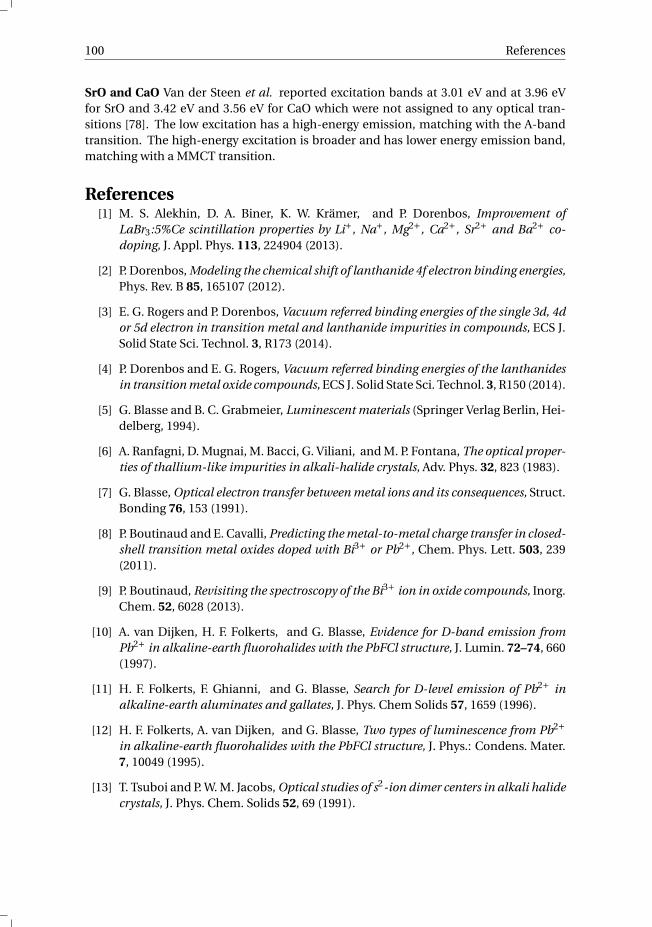
100 References
SrO and CaO Van der Steen et al. reported excitation bands at 3.01 eV and at 3.96 eVfor SrO and 3.42 eV and 3.56 eV for CaO which were not assigned to any optical tran-sitions [78]. The low excitation has a high-energy emission, matching with the A-bandtransition. The high-energy excitation is broader and has lower energy emission band,matching with a MMCT transition.
References[1] M. S. Alekhin, D. A. Biner, K. W. Krämer, and P. Dorenbos, Improvement of
LaBr3:5%Ce scintillation properties by Li+, Na+, Mg2+, Ca2+, Sr2+ and Ba2+ co-doping, J. Appl. Phys. 113, 224904 (2013).
[2] P. Dorenbos, Modeling the chemical shift of lanthanide 4f electron binding energies,Phys. Rev. B 85, 165107 (2012).
[3] E. G. Rogers and P. Dorenbos, Vacuum referred binding energies of the single 3d, 4dor 5d electron in transition metal and lanthanide impurities in compounds, ECS J.Solid State Sci. Technol. 3, R173 (2014).
[4] P. Dorenbos and E. G. Rogers, Vacuum referred binding energies of the lanthanidesin transition metal oxide compounds, ECS J. Solid State Sci. Technol. 3, R150 (2014).
[5] G. Blasse and B. C. Grabmeier, Luminescent materials (Springer Verlag Berlin, Hei-delberg, 1994).
[6] A. Ranfagni, D. Mugnai, M. Bacci, G. Viliani, and M. P. Fontana, The optical proper-ties of thallium-like impurities in alkali-halide crystals, Adv. Phys. 32, 823 (1983).
[7] G. Blasse, Optical electron transfer between metal ions and its consequences, Struct.Bonding 76, 153 (1991).
[8] P. Boutinaud and E. Cavalli, Predicting the metal-to-metal charge transfer in closed-shell transition metal oxides doped with Bi3+ or Pb2+, Chem. Phys. Lett. 503, 239(2011).
[9] P. Boutinaud, Revisiting the spectroscopy of the Bi3+ ion in oxide compounds, Inorg.Chem. 52, 6028 (2013).
[10] A. van Dijken, H. F. Folkerts, and G. Blasse, Evidence for D-band emission fromPb2+ in alkaline-earth fluorohalides with the PbFCl structure, J. Lumin. 72–74, 660(1997).
[11] H. F. Folkerts, F. Ghianni, and G. Blasse, Search for D-level emission of Pb2+ inalkaline-earth aluminates and gallates, J. Phys. Chem Solids 57, 1659 (1996).
[12] H. F. Folkerts, A. van Dijken, and G. Blasse, Two types of luminescence from Pb2+in alkaline-earth fluorohalides with the PbFCl structure, J. Phys.: Condens. Mater.7, 10049 (1995).
[13] T. Tsuboi and P. W. M. Jacobs, Optical studies of s2-ion dimer centers in alkali halidecrystals, J. Phys. Chem. Solids 52, 69 (1991).
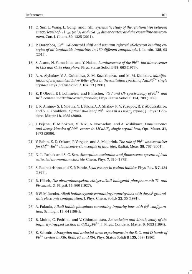
References 101
[14] Q. Sun, L. Wang, L. Gong, and J. Shi, Systematic study of the relationships betweenenergy levels of (Tl+)2, (In+)2 and (Ga+)2 dimer centers and the crystalline environ-ment, Can. J. Chem. 89, 1325 (2011).
[15] P. Dorenbos, Ce3+ 5d-centroid shift and vacuum referred 4f-electron binding en-ergies of all lanthanide impurities in 150 different compounds, J. Lumin. 135, 93(2013).
[16] S. Asano, N. Yamashita, and Y. Nakao, Luminescence of the Pb2+-ion dimer centerin CaS and CaSe phosphors, Phys. Status Solidi B 89, 663 (1978).
[17] A. A. Alybakov, V. A. Gubanova, Z. M. Kazakbaeva, and M. M. Kidibaev, Manifes-tation of a dynamical Jahn-Teller effect in the excitation spectra of NaI:Pb2+ singlecrystals, Phys. Status Solidi A 167, 73 (1991).
[18] K. P. Oboth, F. J. Lohmeier, and F. Fischer, VUV and UV spectroscopy of Pb2+ andBi3+ centres in alkaline-earth fluorides, Phys. Status Solidi B 154, 789 (1989).
[19] L. K. Aminov, S. I. Nikitin, N. I. Silkin, A. A. Shakov, R. V. Yusupov, R. Y. Abdulsabirov,and S. L. Korableva, Optical studies of Pb2+ ions in a LiBaF3 crystal, J. Phys.: Con-dens. Matter 18, 4985 (2006).
[20] J. Pejchal, E. Mihokova, M. Nikl, A. Novoselov, and A. Yoshikawa, Luminescenceand decay kinetics of Pb2+ center in LiCaAlF6 single crystal host, Opt. Mater. 31,1673 (2009).
[21] V. Babin, K. D. Oskam, P. Vergeer, and A. Meijerink, The role of Pb2+ as a sensitizerfor Gd3+-Eu2+ downconversion couple in fluorides, Radiat. Meas. 38, 767 (2004).
[22] N. L. Pathak and S. C. Sen, Absorption, excitation and fluorescence spectra of leadactivated ammonium chloride, Chem. Phys. 7, 310 (1975).
[23] S. Radhakrishna and K. P. Pande, Lead centers in cesium halides, Phys. Rev. B 7, 424(1973).
[24] R. Hilsch, Die absorptionsspektra einiger alkali-halogenid-phosphore mit Tl- undPb-zusatz, Z. Physik 44, 860 (1927).
[25] P. W. M. Jacobs, Alkali halide crystals containing impurity ions with the ns2 ground-state electronic configuration, J. Phys. Chem. Solids 22, 35 (1991).
[26] A. Fukuda, Alkali halide phosphors containing impurity ions with (s)2 configura-tion, Sci. Light 13, 64 (1964).
[27] B. Moine, C. Pedrini, and V. Ghiordanescu, An emission and kinetic study of theimpurity-trapped exciton in CdCl2:Pb2+, J. Phys.: Condens. Matter 6, 4093 (1994).
[28] K. Schmitt, Absorption and uniaxial stress experiments in the B, C, and D bands ofPb2+ centres in KBr, RbBr, KI, and RbI, Phys. Status Solidi B 135, 389 (1986).
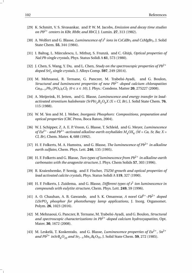
102 References
[29] K. Schmitt, V. S. Sivasankar, and P. W. M. Jacobs, Emission and decay time studieson Pb2+ centers in KBr, RbBr, and RbCl, J. Lumin. 27, 313 (1982).
[30] A. Wolfert and G. Blasse, Luminescence of s2 ions in CsCdBr3 and CsMgBr3, J. SolidState Chem. 55, 344 (1984).
[31] I. Baltog, L. Marculescu, L. Mithut, S. Frunza, and C. Ghita, Optical properties ofNaI:Pb single crystals, Phys. Status Solidi A 61, 573 (1980).
[32] J. Chen, S. Wang, Y. Du, and L. Chen, Study on the spectroscopic properties of Pb2+doped SrI2 single crystals, J. Alloys Comp. 597, 249 (2014).
[33] M. Mehnaoui, R. Ternane, G. Panczer, M. Trabelsi-Ayadi, and G. Boulon,Structural and luminescent properties of new Pb2+-doped calcium chlorapatitesCa10−x Pbx (PO4)6Cl2 (0 ≤ x ≤ 10), J. Phys.: Condens. Matter 20, 275227 (2008).
[34] A. Meijerink, H. Jetten, and G. Blasse, Luminescence and energy transfer in lead-activated strontium haloborate (SrPb)2B5O9X (X = Cl, Br), J. Solid State Chem. 76,115 (1988).
[35] W. M. Yen and M. J. Weber, Inorganic Phosphors: Compositions, preparation andoptical properties (CRC Press, Boca Raton, 2004).
[36] W. J. Schipper, Z. A. E. P. Vroon, G. Blasse, T. Schleid, and G. Meyer, Luminescenceof Eu2+- and Pb2+-activated alkaline-earth oxyhalides M4OX6 (M = Ca, Sr, Ba; X =Cl, Br), Chem. Mater. 4, 688 (1992).
[37] H. F. Folkerts, M. A. Hamstra, and G. Blasse, The luminescence of Pb2+ in alkalineearth sulfates, Chem. Phys. Lett. 246, 135 (1995).
[38] H. F. Folkerts and G. Blasse, Two types of luminescence from Pb2+ in alkaline-earthcarbonates with the aragonite structure, J. Phys. Chem Solids 57, 303 (1996).
[39] R. Kraienhemke, P. Semig, and F. Fischer, TSZM-growth and optical properties oflead activated calcite crystals, Phys. Status Solidi A 119, 327 (1990).
[40] H. F. Folkerts, J. Zuidema, and G. Blasse, Different types of s2 ion luminescence incompounds with eulytite structure, Chem. Phys. Lett. 249, 59 (1996).
[41] A. O. Chauhan, A. B. Gawande, and S. K. Omanwar, A novel Gd3+-Pb2+ dopedLiSrPO4 phosphor for phototherapy lamp applications, J. Inorg. Organomet.Polym. 26, 1023 (2016).
[42] M. Mehnaoui, G. Panczer, R. Ternane, M. Trabelsi-Ayadi, and G. Boulon, Structuraland spectroscopic characterizations in Pb2+-doped calcium hydroxyapatites, Opt.Mater. 30, 1672 (2008).
[43] M. Leskelä, T. Koskentalo, and G. Blasse, Luminescence properties of Eu2+, Sn2+and Pb2+ inSrB6O10 and Sr1−x Mnx B6O10, J. Solid State Chem. 59, 272 (1985).
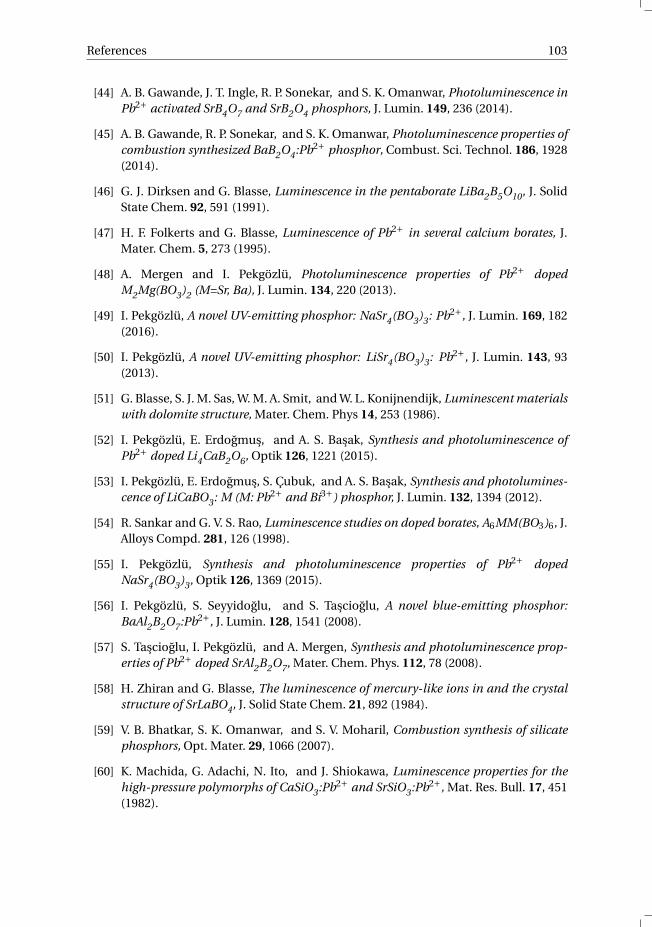
References 103
[44] A. B. Gawande, J. T. Ingle, R. P. Sonekar, and S. K. Omanwar, Photoluminescence inPb2+ activated SrB4O7 and SrB2O4 phosphors, J. Lumin. 149, 236 (2014).
[45] A. B. Gawande, R. P. Sonekar, and S. K. Omanwar, Photoluminescence properties ofcombustion synthesized BaB2O4:Pb2+ phosphor, Combust. Sci. Technol. 186, 1928(2014).
[46] G. J. Dirksen and G. Blasse, Luminescence in the pentaborate LiBa2B5O10, J. SolidState Chem. 92, 591 (1991).
[47] H. F. Folkerts and G. Blasse, Luminescence of Pb2+ in several calcium borates, J.Mater. Chem. 5, 273 (1995).
[48] A. Mergen and I. Pekgözlü, Photoluminescence properties of Pb2+ dopedM2Mg(BO3)2 (M=Sr, Ba), J. Lumin. 134, 220 (2013).
[49] I. Pekgözlü, A novel UV-emitting phosphor: NaSr4(BO3)3: Pb2+, J. Lumin. 169, 182(2016).
[50] I. Pekgözlü, A novel UV-emitting phosphor: LiSr4(BO3)3: Pb2+, J. Lumin. 143, 93(2013).
[51] G. Blasse, S. J. M. Sas, W. M. A. Smit, and W. L. Konijnendijk, Luminescent materialswith dolomite structure, Mater. Chem. Phys 14, 253 (1986).
[52] I. Pekgözlü, E. Erdogmus, and A. S. Basak, Synthesis and photoluminescence ofPb2+ doped Li4CaB2O6, Optik 126, 1221 (2015).
[53] I. Pekgözlü, E. Erdogmus, S. Çubuk, and A. S. Basak, Synthesis and photolumines-cence of LiCaBO3: M (M: Pb2+ and Bi3+) phosphor, J. Lumin. 132, 1394 (2012).
[54] R. Sankar and G. V. S. Rao, Luminescence studies on doped borates, A6MM(BO3)6, J.Alloys Compd. 281, 126 (1998).
[55] I. Pekgözlü, Synthesis and photoluminescence properties of Pb2+ dopedNaSr4(BO3)3, Optik 126, 1369 (2015).
[56] I. Pekgözlü, S. Seyyidoglu, and S. Tascioglu, A novel blue-emitting phosphor:BaAl2B2O7:Pb2+, J. Lumin. 128, 1541 (2008).
[57] S. Tascioglu, I. Pekgözlü, and A. Mergen, Synthesis and photoluminescence prop-erties of Pb2+ doped SrAl2B2O7, Mater. Chem. Phys. 112, 78 (2008).
[58] H. Zhiran and G. Blasse, The luminescence of mercury-like ions in and the crystalstructure of SrLaBO4, J. Solid State Chem. 21, 892 (1984).
[59] V. B. Bhatkar, S. K. Omanwar, and S. V. Moharil, Combustion synthesis of silicatephosphors, Opt. Mater. 29, 1066 (2007).
[60] K. Machida, G. Adachi, N. Ito, and J. Shiokawa, Luminescence properties for thehigh-pressure polymorphs of CaSiO3:Pb2+ and SrSiO3:Pb2+, Mat. Res. Bull. 17, 451(1982).
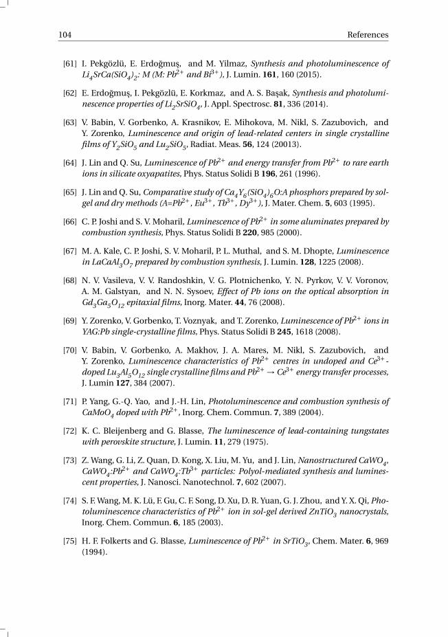
104 References
[61] I. Pekgözlü, E. Erdogmus, and M. Yilmaz, Synthesis and photoluminescence ofLi4SrCa(SiO4)2: M (M: Pb2+ and Bi3+), J. Lumin. 161, 160 (2015).
[62] E. Erdogmus, I. Pekgözlü, E. Korkmaz, and A. S. Basak, Synthesis and photolumi-nescence properties of Li2SrSiO4, J. Appl. Spectrosc. 81, 336 (2014).
[63] V. Babin, V. Gorbenko, A. Krasnikov, E. Mihokova, M. Nikl, S. Zazubovich, andY. Zorenko, Luminescence and origin of lead-related centers in single crystallinefilms of Y2SiO5 and Lu2SiO5, Radiat. Meas. 56, 124 (20013).
[64] J. Lin and Q. Su, Luminescence of Pb2+ and energy transfer from Pb2+ to rare earthions in silicate oxyapatites, Phys. Status Solidi B 196, 261 (1996).
[65] J. Lin and Q. Su, Comparative study of Ca4Y6(SiO4)6O:A phosphors prepared by sol-gel and dry methods (A=Pb2+, Eu3+, Tb3+, Dy3+), J. Mater. Chem. 5, 603 (1995).
[66] C. P. Joshi and S. V. Moharil, Luminescence of Pb2+ in some aluminates prepared bycombustion synthesis, Phys. Status Solidi B 220, 985 (2000).
[67] M. A. Kale, C. P. Joshi, S. V. Moharil, P. L. Muthal, and S. M. Dhopte, Luminescencein LaCaAl3O7 prepared by combustion synthesis, J. Lumin. 128, 1225 (2008).
[68] N. V. Vasileva, V. V. Randoshkin, V. G. Plotnichenko, Y. N. Pyrkov, V. V. Voronov,A. M. Galstyan, and N. N. Sysoev, Effect of Pb ions on the optical absorption inGd3Ga5O12 epitaxial films, Inorg. Mater. 44, 76 (2008).
[69] Y. Zorenko, V. Gorbenko, T. Voznyak, and T. Zorenko, Luminescence of Pb2+ ions inYAG:Pb single-crystalline films, Phys. Status Solidi B 245, 1618 (2008).
[70] V. Babin, V. Gorbenko, A. Makhov, J. A. Mares, M. Nikl, S. Zazubovich, andY. Zorenko, Luminescence characteristics of Pb2+ centres in undoped and Ce3+-doped Lu3Al5O12 single crystalline films and Pb2+ → Ce3+ energy transfer processes,J. Lumin 127, 384 (2007).
[71] P. Yang, G.-Q. Yao, and J.-H. Lin, Photoluminescence and combustion synthesis ofCaMoO4 doped with Pb2+, Inorg. Chem. Commun. 7, 389 (2004).
[72] K. C. Bleijenberg and G. Blasse, The luminescence of lead-containing tungstateswith perovskite structure, J. Lumin. 11, 279 (1975).
[73] Z. Wang, G. Li, Z. Quan, D. Kong, X. Liu, M. Yu, and J. Lin, Nanostructured CaWO4,CaWO4:Pb2+ and CaWO4:Tb3+ particles: Polyol-mediated synthesis and lumines-cent properties, J. Nanosci. Nanotechnol. 7, 602 (2007).
[74] S. F. Wang, M. K. Lü, F. Gu, C. F. Song, D. Xu, D. R. Yuan, G. J. Zhou, and Y. X. Qi, Pho-toluminescence characteristics of Pb2+ ion in sol-gel derived ZnTiO3 nanocrystals,Inorg. Chem. Commun. 6, 185 (2003).
[75] H. F. Folkerts and G. Blasse, Luminescence of Pb2+ in SrTiO3, Chem. Mater. 6, 969(1994).
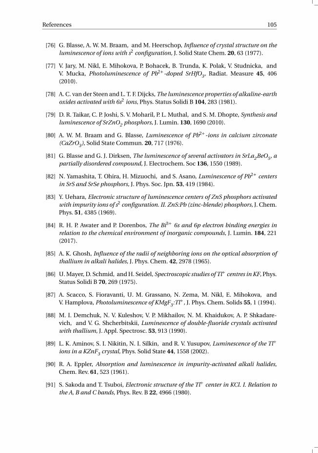
References 105
[76] G. Blasse, A. W. M. Braam, and M. Heerschop, Influence of crystal structure on theluminescence of ions with s2 configuration, J. Solid State Chem. 20, 63 (1977).
[77] V. Jary, M. Nikl, E. Mihokova, P. Bohacek, B. Trunda, K. Polak, V. Studnicka, andV. Mucka, Photoluminescence of Pb2+-doped SrHfO3, Radiat. Measure 45, 406(2010).
[78] A. C. van der Steen and L. T. F. Dijcks, The luminescence properties of alkaline-earthoxides activated with 6s2 ions, Phys. Status Solidi B 104, 283 (1981).
[79] D. R. Taikar, C. P. Joshi, S. V. Moharil, P. L. Muthal, and S. M. Dhopte, Synthesis andluminescence of SrZnO2 phosphors, J. Lumin. 130, 1690 (2010).
[80] A. W. M. Braam and G. Blasse, Luminescence of Pb2+-ions in calcium zirconate(CaZrO3), Solid State Commun. 20, 717 (1976).
[81] G. Blasse and G. J. Dirksen, The luminescence of several activators in SrLa2BeO5, apartially disordered compound, J. Electrochem. Soc 136, 1550 (1989).
[82] N. Yamashita, T. Ohira, H. Mizuochi, and S. Asano, Luminescence of Pb2+ centersin SrS and SrSe phosphors, J. Phys. Soc. Jpn. 53, 419 (1984).
[83] Y. Uehara, Electronic structure of luminescence centers of ZnS phosphors activatedwith impurity ions of s2 configuration. II. ZnS:Pb (zinc-blende) phosphors, J. Chem.Phys. 51, 4385 (1969).
[84] R. H. P. Awater and P. Dorenbos, The Bi3+ 6s and 6p electron binding energies inrelation to the chemical environment of inorganic compounds, J. Lumin. 184, 221(2017).
[85] A. K. Ghosh, Influence of the radii of neighboring ions on the optical absorption ofthallium in alkali halides, J. Phys. Chem. 42, 2978 (1965).
[86] U. Mayer, D. Schmid, and H. Seidel, Spectroscopic studies of Tl+ centres in KF, Phys.Status Solidi B 70, 269 (1975).
[87] A. Scacco, S. Fioravanti, U. M. Grassano, N. Zema, M. Nikl, E. Mihokova, andV. Hamplova, Photoluminescence of KMgF3:Tl+, J. Phys. Chem. Solids 55, 1 (1994).
[88] M. I. Demchuk, N. V. Kuleshov, V. P. Mikhailov, N. M. Khaidukov, A. P. Shkadare-vich, and V. G. Shcherbitskii, Luminescence of double-fluoride crystals activatedwith thallium, J. Appl. Spectrosc. 53, 913 (1990).
[89] L. K. Aminov, S. I. Nikitin, N. I. Silkin, and R. V. Yusupov, Luminescence of the Tl+ions in a KZnF3 crystal, Phys. Solid State 44, 1558 (2002).
[90] R. A. Eppler, Absorption and luminescence in impurity-activated alkali halides,Chem. Rev. 61, 523 (1961).
[91] S. Sakoda and T. Tsuboi, Electronic structure of the Tl+ center in KCl. I. Relation tothe A, B and C bands, Phys. Rev. B 22, 4966 (1980).
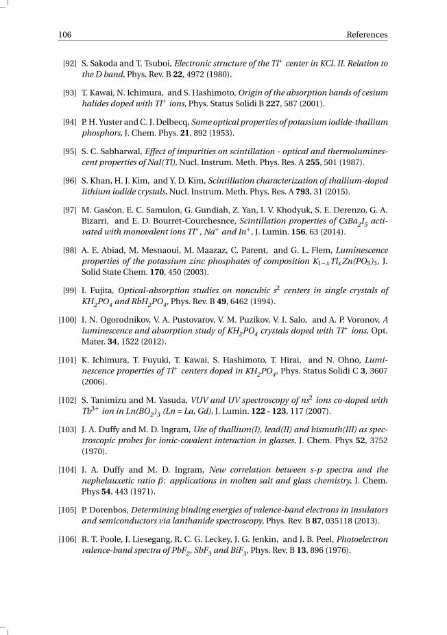
106 References
[92] S. Sakoda and T. Tsuboi, Electronic structure of the Tl+ center in KCl. II. Relation tothe D band, Phys. Rev. B 22, 4972 (1980).
[93] T. Kawai, N. Ichimura, and S. Hashimoto, Origin of the absorption bands of cesiumhalides doped with Tl+ ions, Phys. Status Solidi B 227, 587 (2001).
[94] P. H. Yuster and C. J. Delbecq, Some optical properties of potassium iodide-thalliumphosphors, J. Chem. Phys. 21, 892 (1953).
[95] S. C. Sabharwal, Effect of impurities on scintillation - optical and thermolumines-cent properties of NaI(Tl), Nucl. Instrum. Meth. Phys. Res. A 255, 501 (1987).
[96] S. Khan, H. J. Kim, and Y. D. Kim, Scintillation characterization of thallium-dopedlithium iodide crystals, Nucl. Instrum. Meth. Phys. Res. A 793, 31 (2015).
[97] M. Gascon, E. C. Samulon, G. Gundiah, Z. Yan, I. V. Khodyuk, S. E. Derenzo, G. A.Bizarri, and E. D. Bourret-Courchesnce, Scintillation properties of CsBa2I5 acti-vated with monovalent ions Tl+, Na+ and In+, J. Lumin. 156, 63 (2014).
[98] A. E. Abiad, M. Mesnaoui, M. Maazaz, C. Parent, and G. L. Flem, Luminescenceproperties of the potassium zinc phosphates of composition K1−x Tlx Zn(PO3)3, J.Solid State Chem. 170, 450 (2003).
[99] I. Fujita, Optical-absorption studies on noncubic s2 centers in single crystals ofKH2PO4 and RbH2PO4, Phys. Rev. B 49, 6462 (1994).
[100] I. N. Ogorodnikov, V. A. Pustovarov, V. M. Puzikov, V. I. Salo, and A. P. Voronov, Aluminescence and absorption study of KH2PO4 crystals doped with Tl+ ions, Opt.Mater. 34, 1522 (2012).
[101] K. Ichimura, T. Fuyuki, T. Kawai, S. Hashimoto, T. Hirai, and N. Ohno, Lumi-nescence properties of Tl+ centers doped in KH2PO4, Phys. Status Solidi C 3, 3607(2006).
[102] S. Tanimizu and M. Yasuda, VUV and UV spectroscopy of ns2 ions co-doped withTb3+ ion in Ln(BO2)3 (Ln = La, Gd), J. Lumin. 122 - 123, 117 (2007).
[103] J. A. Duffy and M. D. Ingram, Use of thallium(I), lead(II) and bismuth(III) as spec-troscopic probes for ionic-covalent interaction in glasses, J. Chem. Phys 52, 3752(1970).
[104] J. A. Duffy and M. D. Ingram, New correlation between s-p spectra and thenephelauxetic ratio β: applications in molten salt and glass chemistry, J. Chem.Phys 54, 443 (1971).
[105] P. Dorenbos, Determining binding energies of valence-band electrons in insulatorsand semiconductors via lanthanide spectroscopy, Phys. Rev. B 87, 035118 (2013).
[106] R. T. Poole, J. Liesegang, R. C. G. Leckey, J. G. Jenkin, and J. B. Peel, Photoelectronvalence-band spectra of PbF2, SbF3 and BiF3, Phys. Rev. B 13, 896 (1976).
References 107
[107] R. D. Shannon, Revised effective ionic radii and systematic studies of interatomicdistances in halides and chalcogenides, Acta Cryst. 32, 751 (1976).
[108] R. H. P. Awater and P. Dorenbos, Towards a general concentration quenching modelof Bi3+ luminescence, J. Lumin. 188, 487 (2017).
[109] P. Dorenbos, Electron binding energies and how it relates to activator luminescenceand bonding in compounds, J. Lumin. 169, 381 (2016).
[110] R. Hawrami, E. Ariesanti, L. S. Pandian, J. Glodo, and K. S. Shah, Tl2LiLaBr6:Ce andTl2LiYCl6:Ce3+: new elpasolite scintillators, Proc. IEEE NSS/MIC , 1 (2015).
[111] H. J. Kim, G. Rooh, and S. Kim, Tl2LaCl5(Ce3+): new fast and efficient scintillatorfor X- and γ-ray detection, J. Lumin. 186, 219 (2017).
[112] H. J. Kim, G. Rooh, A. Khan, and S. Kim, New Tl2LaBr5:Ce3+ crystal scintillator forγ-rays detection, Nucl. Instrum. Meth. Phys. Res. A 849, 72 (2017).
[113] Q. Sun, H. Dai, L. Wang, J. Wang, and J. Shi, Investigation of relationships betweenabsorption band energies of Tl+ and the crystalline environment, Mater. Chem.Phys. 132, 895 (2012).

Summary
Scintillation materials convert high-energy radiation into many visible photons and, incombination with a photodetector, are used as ionizing radiation detectors. Since thediscovery of ionizing radiation, there have been intensive research efforts in finding new,better performing scintillators, resulting in the development of a large variety of scintil-lation materials. Each scintillation material is tailored to a specific application to havethe best performance. With ever-increasing material demands set by the various appli-cations of scintillators, the search for even better performing scintillation materials re-mains an active field. This thesis explores new avenues of scintillation materials researchin order to find the next-generation of scintillation materials.
A valuable technique to improve the scintillation properties of existing scintillationmaterials is by means of co-doping. Chapter 2 discusses the effects of Na+, Mg2+, Ca2+,Sr2+ and Ba2+ doping on the scintillation properties of CeBr3. Adding a small amount ofaliovalent dopant ions has a pronounced effect on the scintillation properties of CeBr3.Ca2+ and Sr2+ doped CeBr3 show an additional perturbed Ce3+ site in the photolumi-nescence and X-ray excited luminescence spectra. Furthermore, these crystals show anearly constant light yield below 300 K, an increased decay time and the appearance ofmultiple glow peaks in the thermoluminescence spectra. We proposed that bromine va-cancies, formed as charge compensation for the aliovalent dopants, act as electron trapswhich can then explain the different scintillation behavior of Ca2+ and Sr2+ doped CeBr3.
In chapters 3 and 4 we investigate the potential of Bi2+, a relatively new dopant ion inthe field of scintillation materials with red-to-infrared emission wavelengths. Chapter 3discusses the X-ray induced valence change of Bi3+ to Bi2+ and the luminescence andscintillation properties of bismuth doped Li2BaP2O7. Although absorption measure-ments show that Bi3+ is present in the as-prepared Li2BaP2O7:Bi, no bismuth-relatedphotoluminescence is observed even at temperatures as low as 10 K. However, during X-ray excitation the characteristic deep-red radioluminescence of Bi2+ is observed. AfterX-ray irradiation, the red luminescence of Bi2+ can be excited optically, indicating thatupon X-ray irradiation the Bi3+ is reduced to Bi2+. Chapter 4 deals with the luminescenceand charge carrier trapping in YPO4:Bi. X-ray excited luminescence measurements showemission from isolated Bi3+, Bi-pairs and Bi2+. Thermoluminescence measurements ofYPO4 doped with Bi3+ and/or Tb3+ show that bismuth can act both as electron and ashole trap. The spectroscopic data obtained in chapters 3 and 4 are used to locate the elec-tron binding energies in the ground and excited states of Bi3+ and Bi2+ inside the vacuumreferred binding energy diagrams of Li2BaP2O7 and YPO4, respectively. The constructedVRBE diagrams provide an interpretation for the commonly observed Bi-pair emission.
109
110 Summary
Currently most research is focused on halide crystals with lanthanide dopants andCe3+ and Eu2+ in particular. These crystals have a rather low density of at maximumaround 6 g/cm3, while scintillation materials with the highest density and stopping powerare needed for radiation detectors in the next-generation of particle colliders and otherhigh-energy physics experiments. To find new and denser scintillation materials, oxidematerials with densities that can go beyond 8 g/cm3 are attractive candidates. To ensurea high stopping power, oxides containing elements with a high atomic number such asTl, Pb and Bi are among the most promising materials. In order to evaluate if Ce3+ canluminescence efficiently in these type of host compounds, knowledge on the impuritylevels of Tl+, Pb2+ and Bi3+ relative to the host conduction and valence bands is required.The electron binding energies in the impurity levels of Bi3+ and how these change in re-lation to the chemical environment are discussed in chapter 5, while those of Tl+ andPb2+ are discussed in chapter 7. To determine these vacuum referred electron bindingenergies, spectroscopic data on the metal-to-metal charge transfer and interconfigura-tional A- and C-band transitions of Tl+, Pb2+ and Bi3+ were collected form the archivalliterature. The VRBE in the 3P1 excited state and 1S0 ground state of Tl+, Pb2+ and Bi3+decreases linearly with the U value of the host compound and follow the nephelauxeticsequence. The chemical shift of Tl+, Pb2+ and Bi3+ increases approximately in the ratio1:2:3, which is similar to the ratio in the amount of screening charge. Although the dif-ference in the amount of screening charge around the dopant ion when incorporated ina compound, the ground state of Tl+, Pb2+ and Bi3+ shift to almost the same energy. Itwas found that the simple chemical shift model that can satisfactorily model the 4f elec-tron binding energies of the lanthanide ions, does not apply to the 6s electron bindingenergies of Tl+, Pb2+ and Bi3+. Apparently the interaction between the electrons in thespatially extended 6s orbital and the surrounding anion orbitals is larger than that of 4fthe atomic-like electrons. Based on the determined VRBEs of the electron in the 3P1 and1S0 states, it is unlikely that Ce3+ will luminescence in Tl-, Pb- or Bi- based oxide com-pounds. However, this research provides new directions for further exploration of highdensity, high stopping power scintillation materials, namely to evaluate if Pb2+ will showluminescence in a Bi-compound or Bi3+ in a Pb-compound. Also the possibility of Tl+,Pb2+ and Bi3+ as activator in suitable, dense host compounds could be explored.
In chapter 6 we show that in general the VRBE in the Bi2+ ground state is located atlower energy as compared to the VRBE in the 3P1 excited state of Bi3+. In the presence ofBi-pairs, it is then upon excitation of one Bi3+ energetically favorable for electron trans-fer to occur, and to form a Bi2+–Bi4+ pair. The recombination of the electron and holeon the Bi2+–Bi4+ pair can occur non-radiatively or radiatively, in the later case the result-ing visible emission band is often observed and ascribed to pair emission. The proposedmechanism of charge transfer between Bi-pairs can also explain the quenching behaviorof Bi3+ luminescence when the Bi3+ concentration increases.
Samenvatting
Scintillatie materialen zetten hoogenergetische straling om in zichtbaar licht en wordenin combinatie met een fotodetector gebruikt als stralingsdetector. Sinds de ontdekkingvan ioniserende straling is er intensief onderzoek naar nieuwe en betere scintillatie ma-terialen. In de loop der jaren zijn er diverse scintillatie materialen ontwikkeld die zijnafgestemd op de specifieke eisen van de verschillende toepassingen. De eisen die aanscintillatie materialen worden gesteld, worden steeds strikter waardoor het onderzoeks-veld naar scintillatie materialen nog steeds zeer actief is. In dit proefschrift verkennenwe nog onbekend terrein in het onderzoek naar scintillatie materialen met als doel omde volgende generatie aan scintillatie materialen te vinden.
Een waardevolle techniek om de scintillatie eigenschappen van een materiaal te ver-beteren is door middel van co-dotering. In hoofdstuk 2 worden de effecten van Na+,Mg2+, Ca2+, Sr2+ en Ba2+ dotering op de scintillatie eigenschappen van CeBr3 bespro-ken. Het toevoegen van een kleine hoeveelheid aan doterings ion heeft een signifi-cante invloed op de scintillatie eigenschappen van CeBr3. Voor Ca2+ en Sr2+ gedoteerdCeBr3 wordt een verstoorde Ce3+ roosterlocatie waargenomen in de foto- en Röntgen-geëxciteerde emissie spectra. Verder hebben deze gedoteerde kristallen een bijna con-stante lichtopbrengst boven 300 K, een langere vervaltijd en meerdere gloeipieken in hetthermoluminescentie spectrum. Ons voorstel is dat broom vacatures die gevormd zijnom de lading van het doterings ion te compenseren, werken als elektron vangstcentrawat het afwijkende scintillatie gedrag van Ca2+ en Sr2+ gedoteerd CeBr3 kan verklaren.
In hoofdstukken 3 en 4 onderzoeken we Bi2+, een relatief nieuw doterings ion in hetonderzoek naar scintillatie materialen met emissie in het rood tot infrarood. In hoofd-stuk 3 worden de Röntgen geïnduceerde valentie verandering van Bi3+ naar Bi2+ en deluminescentie en scintillatie eigenschappen van bismut gedoteerd Li2BaP2O7 bespro-ken. Ondanks dat absorptie metingen laten zien dat er Bi3+ aanwezig is in het gesynthe-tiseerde Li2BaP2O7:Bi, is er geen bismut-gerelateerde fotoluminescentie waargenomen,zelfs niet wanneer het materiaal wordt afgekoeld tot 10 K. Tijdens Röntgen geëxciteerdeluminescentie metingen wordt echter wel de karakteristieke dieprode radioluminescen-tie van Bi2+ waargenomen. Na Röntgen bestraling is het mogelijk om deze rode lumines-centie ook optisch te exciteren, wat er op duidt dat ten gevolge van de Röntgen stralinghet Bi3+ wordt gereduceerd naar Bi2+. In hoofdstuk 4 worden de luminescentie en de ei-genschap om ladingsdragers in te vangen van bismut in YPO4 besproken. In de Röntgengeëxciteerde luminescentie spectra zijn emissie banden van geïsoleerd Bi3+, Bi-parenen Bi2+ waargenomen. Thermoluminescentie metingen van YPO4 gedoteerd met Bi3+en/of Tb3+ tonen aan dat bismut zowel als elektronen als gaten vangstcentrum kan die-nen. De spectroscopie data uit hoofdstukken 3 en 4 worden gebruikt om de bindings-energieën van elektronen in de grond en aangeslagen toestanden van Bi3+ en Bi2+ te be-palen, welke worden weergegeven in een vacuüm gerefereerd bindingsenergie schema
111
112 Samenvatting
van Li2BaP2O7 en YPO4. Deze VRBE schema’s geven daarnaast een interpretatie voor devaak geobserveerde Bi-paren emissie.
Op dit moment wordt er veel onderzoek gedaan naar halide kristallen met lantha-nide doterings ionen en voornamelijk Ce3+ en Eu2+. Deze kristallen hebben een nogallage dichtheid van maximaal rond de 6 g/cm3, terwijl juist scintillatie materialen meteen zo hoog mogelijke dichtheid en stoppend vermogen nodig zijn voor de stralingsde-tectoren in de volgende generatie deeltjesversnellers en andere hoogenergetische fysicaexperimenten. Om nieuwe materialen te vinden met een nog hogere dichtheid zijn juistoxides met een dichtheid hoger dan 8 g/cm3 het meest interessant. Oxides gebaseerdop Tl, Pb of Bi, elementen met een hoog stoppend vermogen, zijn het meest belovend.Om er achter te komen of Ce3+ luminescentie geeft in dit type materialen, is het nood-zakelijk om te weten hoe de energieniveaus van Tl+, Pb2+ en Bi3+ als doterings ion zichverhouden tot de geleidings en valentie band van het gastrooster. De bindingsenergieënvan de elektronen in de energieniveaus van Bi3+ en hoe deze veranderen in relatie totde chemische omgeving zijn het onderwerp van hoofdstuk 5 en die van Tl+ en Pb2+ vanhoofdstuk 7. Om de VRBEs te bepalen, is de spectroscopische data met betrekking tot demetaal-naar-metaal ladingsoverdracht en interconfigurationele A- en C-band overgan-gen verzameld uit de beschikbare literatuur. De VRBE in de 3P1 aangeslagen toestand ende 1S0 grond toestand van Tl+, Pb2+ en Bi3+ laten een lineaire afname met de U waardevan het gastrooster zien en volgen de nephelauxetic serie. De chemische verschuivingvan Tl+, Pb2+ en Bi3+ neemt ongeveer toe in de verhouding 1:2:3, wat gelijk is aan deverhouding tussen de hoeveelheid aan afschermingslading. Ondanks het verschil in dehoeveelheid aan afschermingslading die de ionen omringt wanneer deze zijn ingebouwdin een gastrooster, verschuift de grond toestand van Tl+, Pb2+ en Bi3+ naar ongeveer de-zelfde energie. Het eenvoudige chemische verschuivings model dat de 4f elektron bin-dingsenergieën van de lanthanide ionen kan voorspellen, blijkt niet te gelden voor de 6selektron bindingsenergieën van Tl+, Pb2+ en Bi3+. Blijkbaar is de interactie tussen deelektronen in de ruimtelijk verspreide 6s orbitalen en de chemische omgeving dusda-nig groter dan die van de gelokaliseerde, atoom-achtige 4f elektronen. Op basis van deVRBEs van de elektronen in de 3P1 en 1S0 toestanden, is het onwaarschijnlijk dat Ce3+luminescentie zal geven in Tl-, Pb- of Bi-gebaseerde oxide verbindingen. Dit onderzoekgeeft echter wel nieuwe richtingen voor verdere verkenning van scintillatie materialenmet een hoge dichtheid en een groot stoppend vermogen. Namelijk, het bekijken ofPb2+ in een Bi-verbinding luminescentie geeft of Bi3+ in een Pb-verbinding. Ook de mo-gelijkheid om Tl+, Pb2+ en Bi3+ te gebruiken als activator in geschikte gastroosters meteen hoge dichtheid zou onderzocht kunnen worden.
In hoofdstuk 6 laten we zien dat de VRBE in de grond toestand van Bi2+ over het alge-meen bij een lagere energie ligt dan de VRBE in de Bi3+ 3P1 aangeslagen toestand. Wan-neer Bi-paren aanwezig zijn, is het energetisch gunstig dat er na excitatie een elektronvan het ene Bi3+ ion wordt overgedragen op het andere ion waarbij zich een Bi2+–Bi4+paar vormt. De recombinatie van het elektron en gat op het Bi2+–Bi4+ paar kan zowelstralingsloos als via de uitzending van een foton, waarbij in het laatste geval de resul-terende zichtbare emissie wordt toegeschreven aan Bi-paar emissie. Dit voorgesteldemechanisme van ladingsoverdracht tussen Bi-paren kan ook het uitdovingsgedrag vanBi3+ luminescentie bij hogere Bi3+ concentraties verklaren.
Dankwoord
Vier jaar onderzoek aan de TU Delft is voorbij gevlogen! Mijn beslissing om naar Delftte verhuizen en promotieonderzoek te gaan doen is een van mijn beste beslissingen ge-weest. Het heeft mij ontzettend veel opgeleverd, niet alleen aan ervaring op het gebiedvan wetenschappelijk onderzoek maar ook op persoonlijk vlak. Het scintillatie onder-zoek was voor mij een compleet nieuw onderwerp waar ik mij volledig in kon verdiepenen veel nieuwe technieken en methoden kon leren. Daarnaast kwam mijn interesse voorde lucht- en ruimtevaart sterk naar boven en daar kan ik mij de komende jaren bij FokkerAerostructures verder in kan verdiepen. Echter het voltooien van een PhD is niet iets watje alleen doet. En daarom ben ik een hoop mensen dankbaar voor hun bijdrage aan ditproefschrift.
Allereerst wil ik mijn ouders bedanken voor hun onvoorwaardelijke vertrouwen ensteun. Door jullie ben ik in staat mijn dromen waar te maken en ben ik geworden wie iknu ben. Natuurlijk wil ik ook mijn geweldige familie bedanken. Jullie begrijpen niet altijdwaar ik mee bezig ben, maar daardoor waardeer ik jullie interesse en steun des te meer.Maikel, jouw wil ik in het bijzonder bedanken voor het coverdesign van dit proefschrift.
Elise, jou ben ik nog het meest dankbaar. Ik kan altijd rekenen op jouw onvoor-waardelijke liefde. Jij laat mij mezelf zijn en samen zijn we een perfect team. Ook wilik mijn tweede familie die ik erbij heb gekregen bedanken voor hun interesse en enthou-siasme voor mijn onderzoek.
Of course this thesis was not possible without the help of my promotor and col-leagues. Pieter, thank you for your supervision the past four years. I am grateful foreverything you thought me, from quantum mechanics to writing papers and from theDorenbos models to presenting science. A big thanks to the technicians for keeping allthe setups up and running. I would like to thank all of my colleagues for their valuablescientific discussions as well as our group activities at ‘t Koepeltje and more. Also I wouldlike to thank Vladimir Ouspenski and colleagues at Saint Gobain for their contributionand industrial view on this project. I am also grateful to Karl Krämer and Daniel Binerfor growing the crystals I have investigated. Thanks to all the other people I met whichI forgot to mention here in making my time as a PhD candidate an incredible experience.
Wie ik als laatste wil bedanken maar zeker niet wil vergeten te vermelden zijn mijngoede vrienden uit Wijchen. Ook al woont het merendeel van ons nu verspreid overNederland en is het contact minder dan voorheen, waardeer ik de momenten dat wesamen een biertje drinken des te meer!
113

Curriculum Vitæ
Roy Hendrikus Petrus AWATER
05-02-1990 Born in Wijchen, The Netherlands.
Education
2013–2017 PhD. in Applied PhysicsDelft University of TechnologyThesis: Exploring next-generation scintillation materialsPromotor: Prof. dr. P. Dorenbos
2011–2013 Master of Science in ChemsitryRadboud University NijmegenGraduation project: Growth of InN by Cl2-based Vapour Phase Epitaxy
2007–2011 Bachelor of Applied Science in Analytical ChemistryHogeschool van Arnhem en Nijmegen / HAN University of Applied ScienceGraduation project: Ohmic contact adhesion to III-V semiconductors
2002–2007 Higher General Secondary Education (HAVO)Maaswaal College Wijchen
115

List of Publications
1. R. H. P. Awater and P. Dorenbos, The vacuum referred electron binding energies inthe 1S0 and 3P1 states of Pb2+ and Tl+ in inorganic compounds, submitted to J.Lumin. (2017).
2. R. H. P. Awater and P. Dorenbos, Towards a General Concentration Quenching Modelof Bi3+ luminescence, J. Lumin. 188C, 487-489 (2017).
3. R. H. P. Awater, L. C. Niemeijer-Berghuijs and P. Dorenbos, Luminescence and ChargeCarrier Trapping in YPO4:Bi, Opt. Mater. 66, 351-355 (2017).
4. R. H. P. Awater and P. Dorenbos, The Bi3+ 6s and 6p Electron Binding Energies inRelation to the Chemical Environment of Inorganic Compounds, J. Lumin. 184,221-231 (2017).
5. R. H. P. Awater and P. Dorenbos, X-ray Induced Valence Change and Vacuum Re-ferred Binding Energies of Bi3+ and Bi2+ in Li2BaP2O7, J. Phys. Chem. C 120, 15114-15118 (2016).
6. M. S. Alekhin, R. H. P. Awater, D. A. Biner, K. W. Krämer, J. T. M. de Haas andP. Dorenbos, Luminescence and Spectroscopic Properties of Sm2+ and Er3+ dopedSrI2, J. Lumin. 167, 347-351 (2015).
7. R. H. P. Awater, K. W. Krämer and P. Dorenbos, Effects of Na+, Mg2+, Ca2+, Sr2+and Ba2+ Doping on the Scintillation Properties of CeBr3, IEEE Trans. Nucl. Sci. 62,2343-2348 (2015).
117