Embed Size (px)
Citation preview
Calhoun: The NPS Institutional Archive
Theses and Dissertations Thesis Collection
1984
Experimental evaluation of a new form of M-ary
(M=8) Phase Shift Keying including design of the
transmitter and receiver.
Thompson, Gregory E.
http://hdl.handle.net/10945/19326


DUDLEY KNOX LIBRARYNAVAL POSTGRADUATE SCHOOLMONTEREY, CALIFORNIA 93343


NAVAL POSTGRADUATE SCHOOL
Monterey, California
THESISEXPERIMENTAL EVALUATION OF A NEW FORM OF
M-ARY (M=8) PHASE SHIFT KEYINGINCLUDING DESIGN OF THE
TRANSMITTER AND RECEIVER
by
Gregory E. Thompson
December 1 984-
Thesis Advisor: G. A. Myers
Approved for public release; distribution unlimited
T224031

SECURITY CLASSIFICATION OF THIS PAGE (Whan Data Entered)
REPORT DOCUMENTATION PAGE READ INSTRUCTIONSBEFORE COMPLETING FORM
1. REPORT NUMBER 2. GOVT ACCESSION NO 3. RECIPIENT'S CATALOG NUMBER
4. TITLE (and Subtitle)
Experimental Evaluation of a New Form ofM-ary (M=8) Phase Shift Keying IncludingDesign of the Transmitter and Receiver
5. TYPE OF REPORT 4 PERIOO COVERED
Master's ThesisDecember 1984
6. PERFORMING ORG. REPORT NUMBER
7. AUTHORfsJ
Gregory E. Thompson
8. CONTRACT OR GRANT NUMBERfaJ
9. PERFORMING ORGANIZATION NAME AND ADDRESS
Naval Postgraduate SchoolMonterey, California 93943
10. PROGRAM ELEMENT. PROJECT, TASKAREA » WORK UNIT NUMBERS
11. CONTROLLING OFFICE NAME AND ADDRESS
Naval Postgraduate SchoolMonterey, California 93943
12. REPORT DATEDecember 1984
13. NUMBER OF PAGES
47U. MONITORING AGENCY NAME 4 ADDRESSf*/ different from Controlling Ottlca) 15. SECURITY CLASS, (of thla report)
15«. DECLASSIFICATION- DOWNGRADINGSCHEDULE
16. DISTRIBUTION ST AT EM EN T (of thl a Report)
Approved for public release; distribution unlimited
17. DISTRIBUTION STATEMENT (ol the abstract entered in Block 20, It different from Report)
18. SUPPLEMENTARY NOTES
19. KEY WOROS (Continue on reverse aide If neceeaary and Identity by block number)
Digital ModulationPhase ModulationPhase Shift KeyingM-ary Digital Modulation
20. ABSTRACT (Continue on reverse aide It neceeaary and Identify by block number)
For transmitting digital information over bandpasschannels, M-ary Phase Shift Keying (PSK) schemes are used to
conserve bandwidth at the expense of signal power. A blockof k bits is used to change the phase of the carrier. Thesek bits represent M possible phase shifts since M = 2 .
Common forms of M-ary PSK use equally spaced phase angles.For example, if M=8 and k=3, 8-ary PSK uses eight phase
DD ,
™NRM
73 1473 EDITION OF 1 NOV 65 IS OBSOLETE
S/N 0102- LF- 014- 6601 1SECURITY CLASSIFICATION OF THIS PAGE (When Data Bntarad)
SECURITY CLASSIFICATION OF THIS PAGE (Whwi Dtm Enffd)
angles spaced 45 degrees apart.This thesis considers a hybrid form of PSK when M=8 and
k=3. Each of eight blocks of data with three bits per blockare represented by different phase shifts of the carrier.The phase angles are chosen to give an equal distancebetween states (symbols) when projected onto the sine axisand the cosine axis of a phasor diagram. Thus, when thethree bits are recovered, using two coherent phase detectors,the separation of the decision regions (voltage levels)are equal. This scheme was evaluated by building a trans-mitter and receiver to implement this 8-ary PSK technique.This method was found to improve the noise performanceover conventional 8-ary PSK schemes by approximately 0.4 dB.
S- N 0102- LF- 014- 6601
SECURITY CLASSIFICATION OF THIS PAGE(TWi»n Datm Enffd)

Approved for public release; distribution is unlimited.
Experimental Evaluation of a New Form ofM-ary (M=8) Phase Shift Keying IncludingDesign of the Transmitter and Receiver
by
Gregory E. IhompsonMajor, United States Marine Corps
B. A., Concordia College, Mcorhead, Minnesota, 1977
Submitted in partial fulfillment of therequirements for the degree of
MASTER OF SCIENCE IN ELECTRICAL ENGINEERING
from the
NAVAL POSTGRAD DATE SCHOOLDecember 1984
ABSTRACT
For transmitting digital information over bandpass chan-
nels, M-ary Phase Shift Keying (PSK) schemes are used to
conserve bandwidth at the expense of signal power. A block
of k bits is used to change the phase of the carrier. These
k bits represent M possible phase shifts since M = 2^ .
Common forms of M-ary PSK use equally spaced phase angles.
For example, if M = 8 and k = 3, 8-ary PSK uses eight phase
angles spaced 45 degrees apart.
This thesis considers a hybrid form of PSK when M=8 and
k=3. Each of eight blocks of data with three bits per block
are represented by different phase shifts of the carrier.
The phase angles are chosen to give an equal distance
between states (symbcls) when projected onto the sine axis
and the cosine axis of a phasor diagram. Thus, when the
three bits are recovered, using two coherent phase detec-
tors, the separation of the decision regions (voltage
levels) are equal. This scheme was evaluated by building a
transmitter and a receiver to implement this 8-ary PSK tech-
nique. This method was found to improve the noise perform-
ance over conventional 8-ary PSK schemes by approximately
0.4 dB.
TABLE OF CONTENTS
I. INTRODUCTION 8
A. BACKGROUND 8
B. PHASE SHIFT KEYING 8
C. A NEW MODULATION TECHNIQUE 10
D. SUMMARY OF RESULTS 11
E. CONTENTS 12
II. TRANSMITTER 13
A. PHASE SHIFTERS 13
B. MULTIPLEXER 17
C. GRAY CODE 17
III. RECEIVER 22
A. PHASE DETECTOR 22
B. INTEGRATE AtiD DUMP 34
C. DECISION CIRCUITRY 34
D. BIT ERROR RATIO DETECTOR 37
IV. RESULTS AND CONCLUSIONS 42
A. THEORY 42
B. STANDARD 8-ARY PSK 43
C. RESULTS 45
D. CONCLUSIONS 45
LIST OF REFERENCES 46
INITIAL DISTRIBUTION LIST 47
LIST OF FIGURES
1. 1 Phasor Diagram for Conventional PSK (M=8) 9
1.2 Phasor Diagram for NEW PSK (M=8) Method 11
2.1 Block Diagram of Transmitter 14
2.2 Circuit Diagram for Positive Phase Angles 15
2.3 Circuit Diagram for Negative Phase Angles 16
2.4 Circuit Diagram for Multiplexer, Inverter, 5
Summer 18
2.5 Photographs of Transmitter Output (Positive
Phase) 19
2.6 Photographs of Transmitter Output (Negative
Phase) 20
3.1 Block Diagram of Branch #1 for Recovery of LSB
& MB 23
3-2 Block Diagram of Branch #2 for Recovery of MSB . . 24
3.3 Photographs of Output of Eranch #1 Phase
Detector 27
3.4 Photographs of Output of Eranch #1 Phase
Detector 28
3.5 Photographs of Output of Eranch #2 Phase
Detector 29
3.6 Photographs of Output of Eranch #2 Phase
Detector 30
3.7 Photographs of Output of Sguarer from Branch #1 . . 31
3.8 Photographs of Output of Sguarer from Branch #1 . . 32
3.9 Circuit Diagram of Phase Detector 33
3.10 Circuit Diagram of Integrate and Dump 35
3.11 Timing Diagram of Integrate and Dump 36
3.12 Photograph of Integrate and Dump 37

3.13 Circuit Diagram of Decisicn Circuitry 38
3.14 logic Diagram of Bit Error Ratio Detector 40
3.15 Timing Diagram of Bit Error Ratio Detector .... 41
4. 1 SNR vs. Probability of Error 8-ary PSK Systems . . 43
4.2 Decision Region Surrounding a Phase Angle 44
I- INT BOD OCT ION
A. BACKGROUND
Today, there is an increasing demand for high-speed
digital communications systems. This demand comes at a time
of decreasing available radio frequency (RF) spectrum.
Therefore the development of bandwidth efficient, low prob-
ability of error, digital modulation schemes becomes
increasingly important.
M-ary digital modulation schemes provide a means of
conserving bandwidth at the expense of increased power
requirements. Thus, M-ary digital modulation schemes can be
used to achieve higher data rates in a given bandwidth. In
an M-ary modulation system, ore of M possible symbols is
transmitted during a signaling interval. Each symbol repre-
sents a block of k data bits where M = 2^ . Each symbol in
the M-ary modulation scheme is identifiable by its phase,
amplitude, or frequency, or a combination of these three.
At the receiver, the symbol is identified and decoded into a
block of k data bits.
B. PHASE SHIFT KEYING
The subject of this report is 8-ary Phase Shift Keying
(PSK) . This is defined as a carrier of fixed frequency,
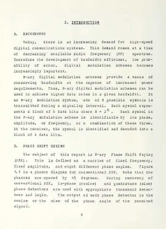
fixed amplitude, and eight different phase angles. Figure
1.1 is a phasor diagram for conventional PSK. Note that the
phasors are spaced by 45 degrees. During recovery of
conventional PSK, in-phase (cosine) and quadrature (sine)
phase detectors are used with appropriate threshold detec-
tors and logic. The output of each phase detector is the
cosine or the sine of the phase angle of the received
signal.
8
100
112.5
101
110
157.5
-157.5
010
111
22.5
0^383 0.924 .COSINE
-22.5
Oil
-112.5
000
67.5
001
Figure 1.1 Phasor Diagram for Conventional PSK (M=8)
9
This output is a voltage that can be processed to recover
the tits originally sent by the transmitter. Figure 1.1
shows these voltage values assuming the circle has a radius
of one. Note that the voltages, which determine the deci-
sion regions, are not separated equally. If a system is
built where these decision regions (voltages) are spaced
equally, it is reasonable to expect better noise perform-
ance. This report examines a communications system built
using a new modulation scheme which accomplishes this.
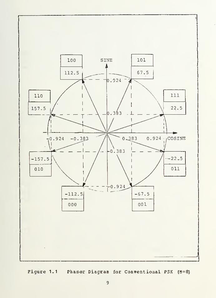
C. A IEH MODULATION TECHNIQUE
The communications system built to incorporate this new
modulation technique consists of a transmitter and a
receiver. The transmitter selects one of eight shifted
carriers corresponding to eight different symbols and trans-
mits it to the receiver.
In the receiver, in-phase and quadrature phase detector's
are used with appropriate threshold detectors and logic to
recover the eight symbols.
Decision theory states for minimum error [Ref. 4 ], deci-
sion regions should be spaced equally. Since a decision is
made based on a certain voltage level (and not on pnase) , it
is reasonable to select phase angles which provide equal
separation of voltage levels cut of the phase detectors.
For example, in Fig. 1.1, although the phases are spaced
equally, the decision regions (voltages) are not.
The solution to accomplishing this can be found using
simple algebra. Figure 1.2 is a phasor diagram of the 8-ary
PSK used in this discussion. Note that the decision regions
are equally separated. The reason, then, for the selection
of this method under study is fcr improved noise performance
over conventional techniques.
10
110
161.6
100
108.4
SINE
i ,
101
71.6
-161.6
010
111
18.4
-108.4
000
-71.6
001
COSINE
-18.4
Oil
Figure 1-2 Phaser Diagram for NEW PSK (M=8) Method
11
D. SUMMARY OF RESULTS
In comparing this new modulation technique (Figure 1.2)
with conventional 8-ary PSK (Figure 1. 1) , the new method
improves the noise performance by approximately 0.4 dB.
This supports the basic premise of this study, that the
phase angles of 8-ary PSK should be chosen so that the sepa-
ration of the decision regions (voltage levels) are equal.
E. CONTENTS
The following chapters of this report consider the
transmitter and the receiver built to study this method and
the results and conclusions of this investigation. Chapter
II describes the transmitter and includes circuit diagrams
of each stage and photographs of the transmitted signal.
The receiver is discussed in chapter III. Circuit diagrams
of the phase detectors, matched filters, and decision logic
are included along with photographs of the output of
selected stages in the receiver circuitry. Chapter IV
contains the detailed results of this report and recommenda-
tions for further study.
12
II. TRANSMITTER
The transmitter is composed of eight phase shifters and
a multiplexer. A block diagram of the transmitter is shown
in Figure 2.1. Also included in the figure are the blocks
for digital data generation, noise generation, and a summer
(adder) to add the signal and the noise. The multiplexer is
the key element of the transmitter. A given three bit
symbol is used to address the cuitiplexer , which selects a
particular one of the eight possible input sinusoids gener-
ated by the the eight phase shifters. Noise is then added
to the phase modulated carrier to simulate a typical
channel.
A. PHASE SHIFTERS
The transmitter requires eight phase shifters to produce
eight sinusoids of the same frequency and amplitude, but
different phase angles. Each phase shifter consists of two
741 op-amps. The first op-amp controls the amplitude and
the second shifts the phase of the cosine carrier. Figures
2.2 and 2.3 show the generation of positive and negative
phase shifts, respectively. The input for this stage is the
carrier, generated by an oscillator operated at the parame-
ters listed below.
Carrier Frequency (f) = 70 kHz
Amplitude =2.0 volts p-p
Phase Angle =0.0
The amount of phase change and amplitude are adjusted by the
two potentiometers.
13
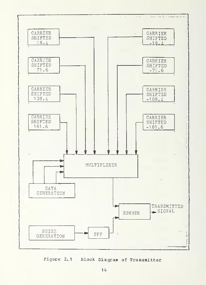
CARRIERSHIFTED
18.4
CARRIERSHIFTED
71 .6
CARRIERSHIFTED108.4
CARRIERSHIFTED161 .6
i ? i f ]}_\[
MULTIPLEXER
DATAGENERATION
NOISEGENERATION BPF
CARRIERSHIFTED-18 . 4
CARRIERSHIFTED-71 .6
CARRIERSHIFTED-1 08.4
CARRIERSHIFTED-1 61 .6
SUMMER
TRANSMITTED.^SIGNAL
Figure 2.
1
Block Diagram of Transmitter
14
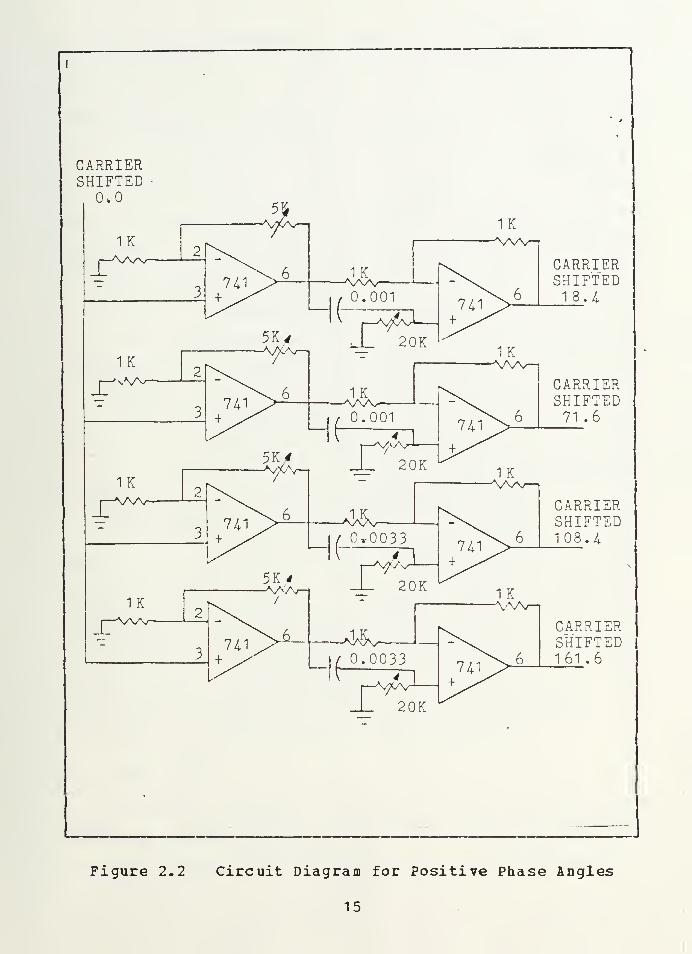
CARRIERSHIFTED
OvO
1K
1K
1K
1K
CARRIERSHIFTED
1 8.4
CARRIERSHIFTED71 .6
CARRIERSHIFTED1 08.4
-A^K0.0033
4
20K
CARRIERSHIFTED161 .6
Figure 2.2 Circuit Diagram for Positive Phase Angles
15
CARRIERSHIFTED
0.0
CARRIERSHIFTED-18.4-
CARRIERSHIFTED-71 .6
CARRIERSHIFTED-108.4.
CARRIERSHIFTED-161 .6
±r 20K
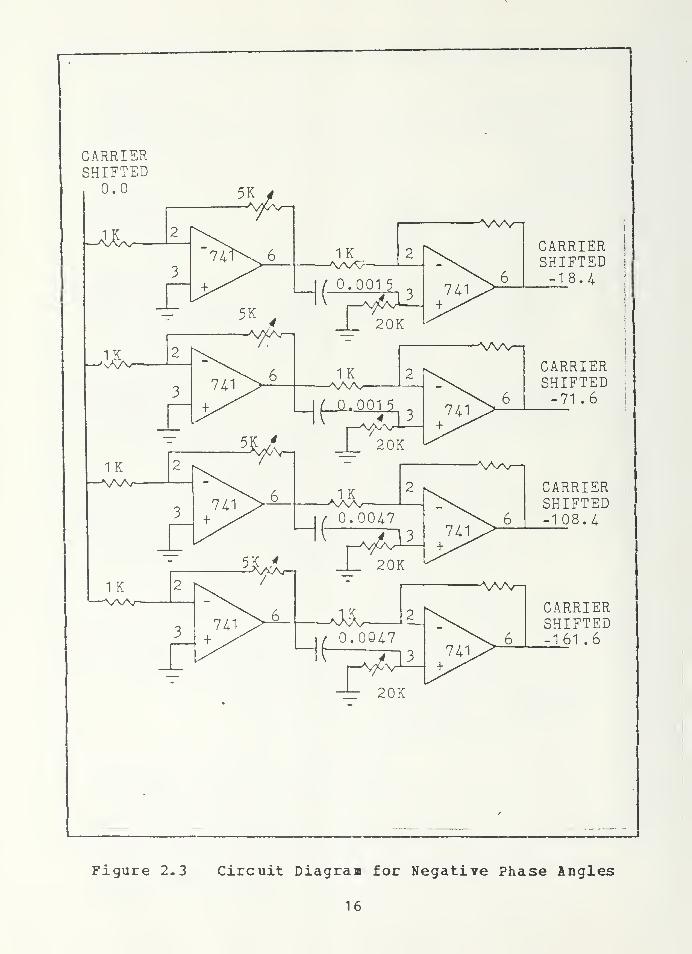
Figure 2.3 Circuit Diagraa for Negative Phase Angles
16 .
All phase adjustments are made using the Hewlett-Packard
Gain Phase Meter Model 3575A [Eef. 1]- In addition to these
eight phase shifters, two more were used to provide refer-
ence sources of 0.0 degrees (cosine) and 90.0 degrees (sine)
to the receiver for coherent phase detection.
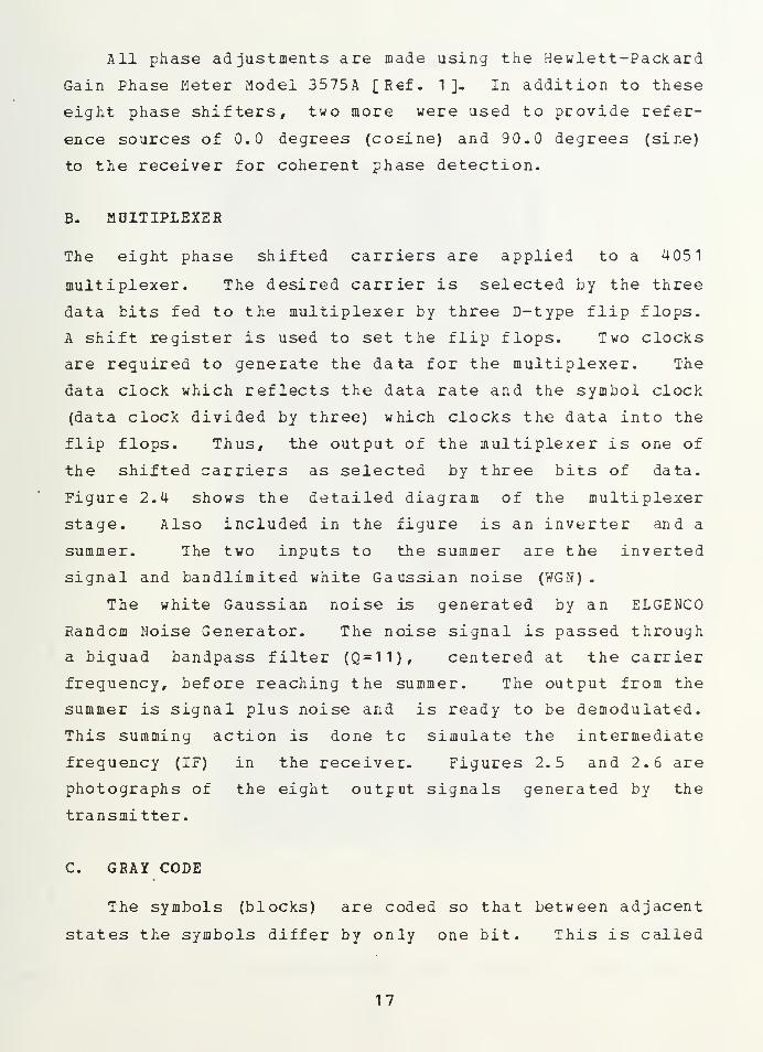
B. MOITIPLEXER
The eight phase shifted carriers are applied to a 4051
multiplexer. The desired carrier is selected by the three
data bits fed to the multiplexer by three D-type flip flops.
A shift register is used to set the flip flops. Two clocks
are required to generate the data for the multiplexer. The
data clock which reflects the data rate and the symbol clock
(data clock divided by three) which clocks the data into the
flip flops. Thus, the output of the multiplexer is one of
the shifted carriers as selected by three bits of data.
Figure 2.4 shows the detailed diagram of the multiplexer
stage. Also included in the figure is an inverter and a
summer. The two inputs to the summer are the inverted
signal and bandlimited white Gaussian noise (WGN)
.
The white Gaussian noise is generated by an ELGENCO
Random Noise Generator. The noise signal is passed through
a biquad bandpass filter (Q=11), centered at the carrier
frequency, before reaching the summer. The output from the
summer is signal plus noise and is ready to be demodulated.
This summing action is done tc simulate the intermediate
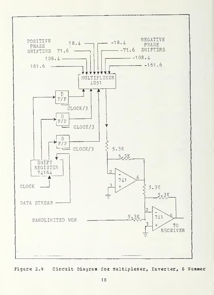
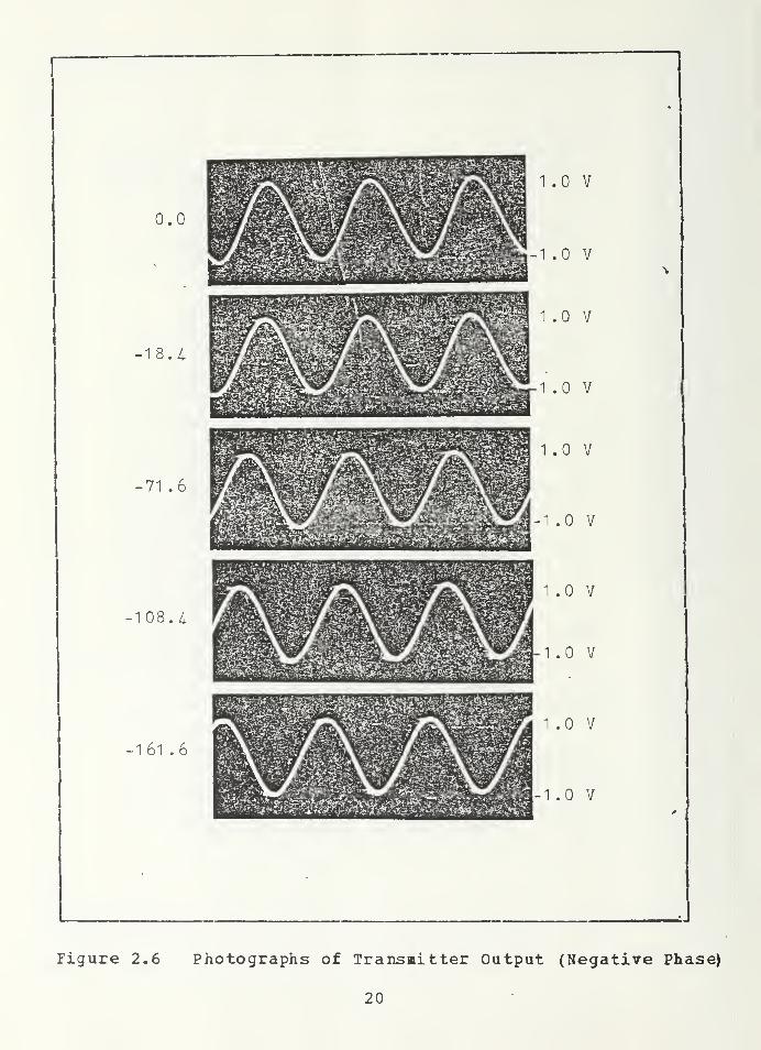
frequency (IF) in the receiver. Figures 2.5 and 2.6 are
photographs of the eight output signals generated by the
transmitter.
C. GRAX CODE
The symbols (blocks) are coded so that between adjacent
states the symbols differ by only one bit. This is called
17
POSITIVEPHASESHIFTERS 71.6
18.4
108. K
161 .6
HiTtTti.
-1 4
• 71.6
NEGATIVEPHASESHIFTERS
-108. k
161.6
MULTIPLEXER4051
D
F/F—
—
t*iCLOCK/3
DF/F
CLOCK/3
D"F/F
CLOCK/3 > 5.3K
fSHIFT
REGISTER7^1 64
A
CLOCK
DATA STREAM
BANDLIMITED WGNTO
RECEIVER
Figure 2-4 Circuit Diagram for Multiplexer, Inverter, C Sumner
18
0.0
18. i
71 .6
108a
161 .6
1 .0 V
-1 .0 V
1.0 V
-1 .0 V
1.0 V
-1.0 V
1.0 V
-1.0 V
1 .0 V
-1.0 V
Figure 2.5 Photographs of Transmitter Output (Positive Phase)
19
0.0
-18.4
-71 .6
-108.4
-161 .6
1 .0 V
-1 .0 V
1.0 V
1.0 V
1 .0 V
-1 .0 V
1 .0 V
-1.0 V
1.0 V
-1.0 V
J
Figure 2.6 Photographs of Transaitter Output (Negative Phase)
20
Gray Coding. Figure 1.2 of the previous chapter is a phasor
diagram showing each phasor with its three bit code. When
an error occurs in transmission, the chosen symbol is most
likely adjacent to the correct symbol (on phasor diagram)
.
Since a symbol has three bits, then if a Gray code is used,
at most one bit will be in error and two bits will be
correct. In other words, the probability of a bit error is
equal to the probability of a symbol error. The other
significant feature of the coding scheme is that the least
significant bit (LSB) is a logical one in the positive half
of the cosine axis and a logical zero in the negative half.
The most significant bit (MSB) is a logical one in the posi-
tive half of the sine axis and is a logical zero in the
negative half. Furthermore, the middle bit (MB) is a
logical one for the phasors vihose absolute value on the
cosine axis is largest and a logical zero for the smaller
absolute value. These facts will aid in the recovery of
each bit and is discussed further in Chapter III.
21
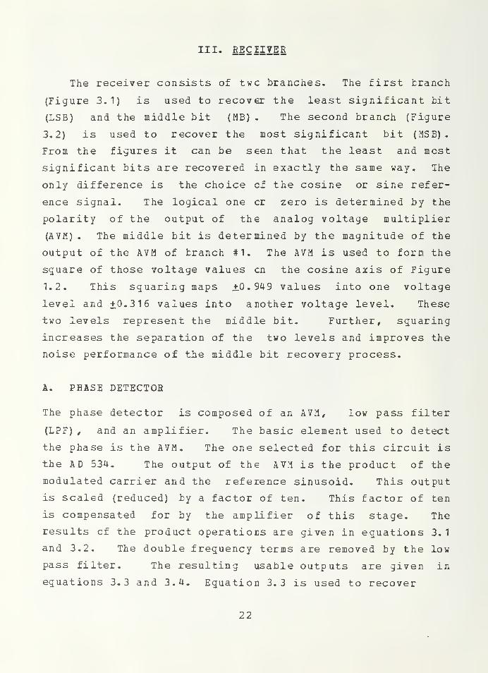
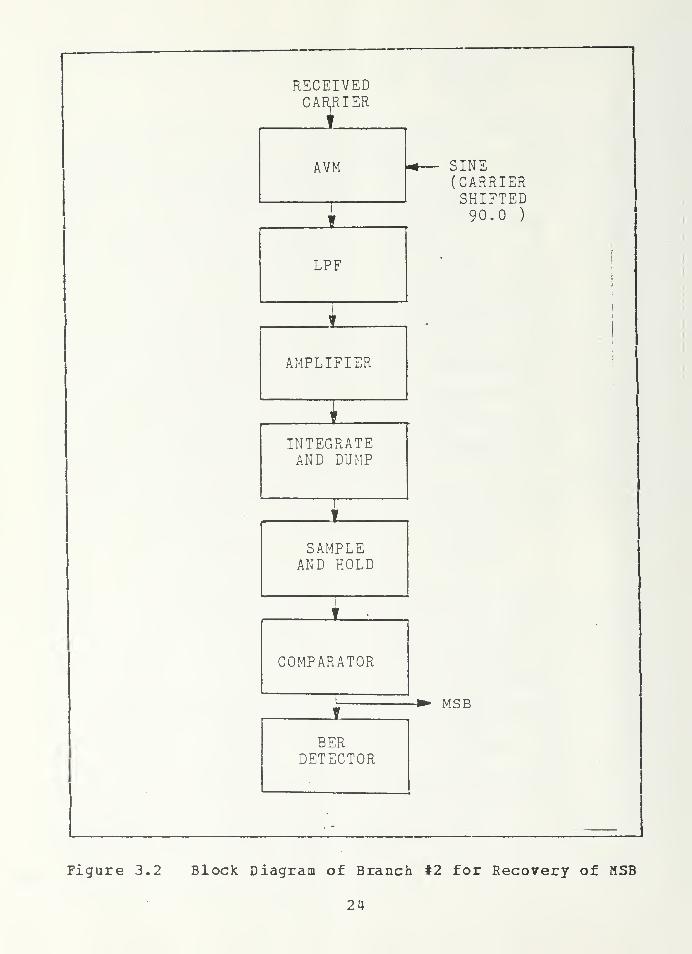
III. RECEIVER
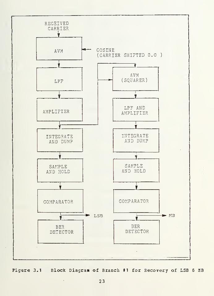
The receiver consists of twc branches. The first tranch
(Figure 3.1) is used to recover the least significant bit
(LSB) and the middle bit (MB) . The second branch (Figure
3.2) is used to recover the most significant bit (MSB).
From the figures it can be seen that the least and most
significant bits are recovered in exactly the same way. The
only difference is the choice of the cosine or sine refer-
ence signal. The logical one cr zero is determined by the
polarity of the output of the analog voltage multiplier
(AVM) . The middle bit is determined by the magnitude of the
output of the AVM of branch #1. The AVM is used to form the
sguare of those voltage values en the cosine axis of Figure
1.2. This squaring maps ±0.949 values into one voltage
level and +0.316 values into another voltage level. These
two levels represent the middle bit. Further, squaring
increases the separation of the two levels and improves the
noise performance of the middle bit recovery process.
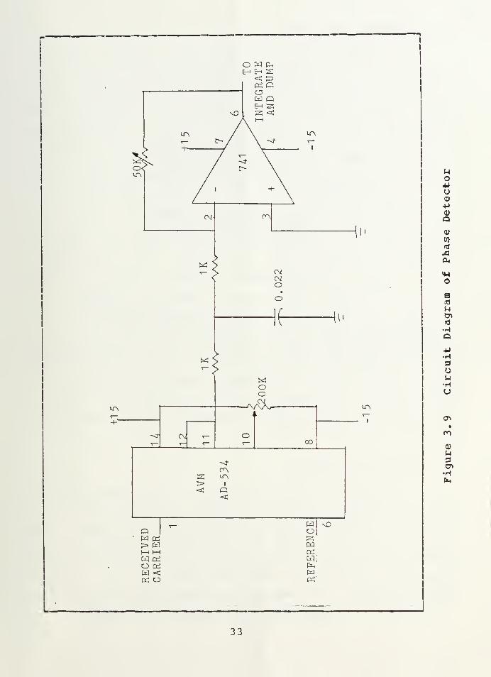
A. PHASE DETECTOE
The phase detector is composed of an AVM, low pass filter
(LPF) , and an amplifier. The basic element used to detect
the phase is the AVM. The one selected for this circuit is
the AD 534. The output of the AVM is the product of the
modulated carrier and the reference sinusoid. This output
is scaled (reduced) by a factor of ten. This factor of ten
is compensated for by the amplifier of this stage. The
results of the product operations are given in equations 3.
1
and 3.2. The double frequency terms are removed by the low
pass filter. The resulting usable outputs are given in
equations 3.3 and 3.4. Equation 3.3 is used to recover
22
RECEIVEDCARRIER
. _ . ,
AVM*— COSINE
(CARRIER SHIFTED 0.0 )
1 *
LPFAVM
(SQUARER)
*1
AMPLIFIERLPF AND
AMPLIFIER
1
*I
INTEGRATEAND DUMP
INTEGRATEAND DUMP
* 4
SAMPLEAND HOLD
SAMPLEAND HOLD
1
*
COMPARATOR COMPARATOR
] SB ir ^ Lf
BERDETECTOR
BERDETECTOR
-
Figure 3.1 Block Diagraa of Branch #1 for Recovery of LSB S MB
23
RECEIVEDCARRIER
±
AMPLIFIER
INTEGRATEAND DUMP
SAMPLEAND HOLD
COMPARATOR
BERDETECTOR
SINE(CARRIERSHIFTED90.0 )
MSB
Figure 3.2 Block Diagram of Branch #2 for Recovery of MSB
24
the least significant bit and the middle bit in branch #1
and equation 3.4 is used to recover the most significant bit
in branch #2.
{cos (w)t) ) (cos (ot+o) ) = 1/2 (cos (2Jt+e) +cos&) (eqn 3.1)
(sin (^t) ) (cos (uot+e-) )=1/2 (sin (2«3t+-&) + sin (-a))
(egn 3.2)
1/2 cos(-e-) (eqn 3.3)
1/2 sin (--©-) (eqn 3.4)
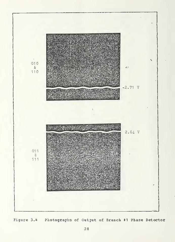
Figures 3.3, 3.4, 3.5, and 3.6 show photographs of the
output of the phase detectors of branches #1 and #2, respec-
tively.
A decision is based on the polarity of the voltages,
namely, logical one for a positive voltage and logical zero
for a negative voltage. The gain factor of the amplifier is
controlled by a potentiometer in the feedback loop. This
allows the output voltage level of the phase detector for
phase angles 71.6 , 108.4 , -71.6 , -108.4 (low value) to be
less than one. This is desirable because in the circuit for
the recovery of the middle bit the AVM is used as a squarer.
Thus, the low magnitude voltage is made relatively smaller
and the high magnitude voltage is made relatively larger. A
decision is based on the difference in magnitude of the
squares of the voltages corresponding to four phase angles
and the other four phase angles 18.4 , 161.6 , -18.4 , and
-161.6 . The photographs of the output of the squarer
amplifier are shown in Figures 3.7 and 3.8 and the detailed
circuitry of the phase detector is shown in Figure 3.9. The
photographs of the output of the squarer show a negative
voltage for two of the cases. This is acheived by biasing
the AVM and the procedure for this is explained in Section
III. C.
25

After carrier detection, the signal is processed into a
usable voltage for the logic circuitry. Processing includes
noise performance improvement using an integrate and dump
circuit and decision circuitry using a sample and hold
device and a comparator.
26

000
100
001&
101
-0.95 V
0.96 V
Figure 3-3 Photographs of Output of Branch #1 Phase Detector
27
010&
110
011&
111
{J
-2.71 V
2.6^ V
Figure 3.4 Photographs of Output of Branch #1 Phase Detector
28
100&
101
000&
001
2.73 V
-2.66 V
Figure 3.5 Photographs of Output of Branch #2 Phase Detector
29
010&
011
110&
111
-0.94. V
0.95 V
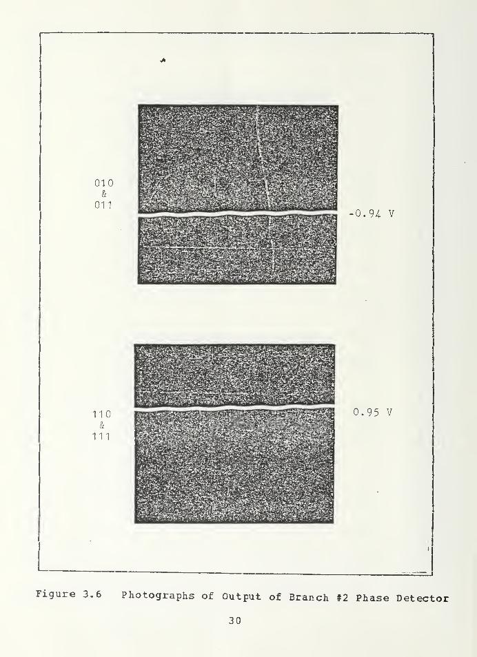
Figure 3.6 Photographs of Output of Branch #2 Phase Detector
30
000&
100
010&
110
-2.86 V
2.95 V
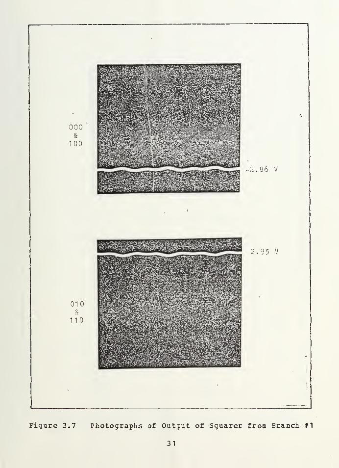
Figure 3-7 Photographs of Output of Sguarer from Branch #1
31
011&
111
001&
101
2.88 V
-2.90 V
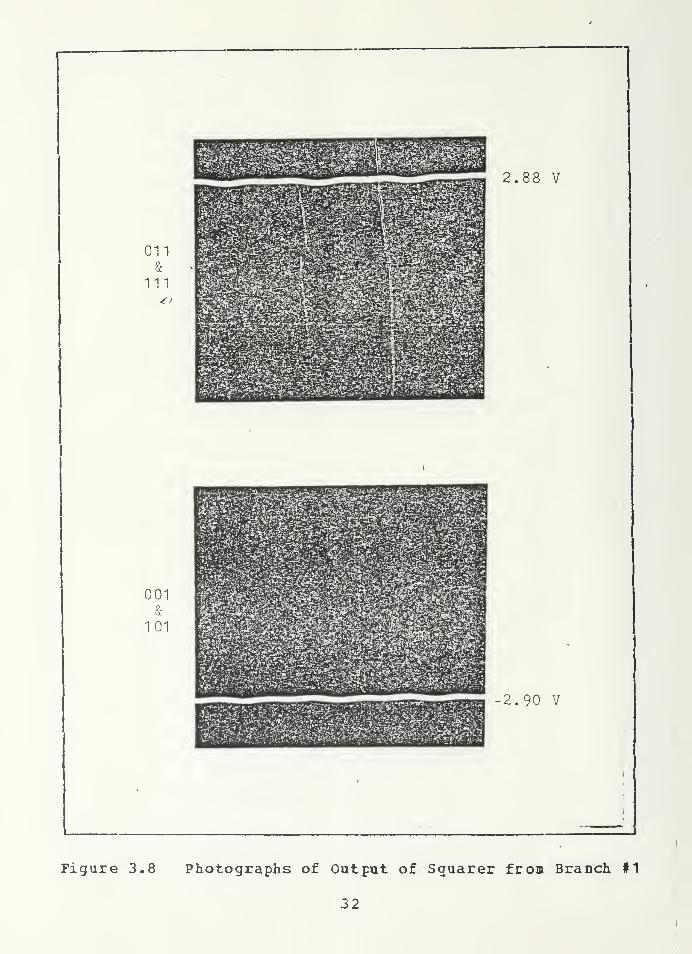
Figure 3.8 Photographs of Output of Sguarer from Branch #1
32
in
in
i
C\J m
^cvo
^
wOO
/\ /\ iin
1 ^
-t-
-<f C\ or—
.T— r- CO
•<*
rns in> 1
< Q<
T w vDQ o
in
i
> wi—1 1—
i
w en:
o c£w <C£ o
o
ud)
M0)
QQ>
W
Cm
M-t
O
aid
M
id
•HQ•M
Uu•HU
m
M
•H
w;
33

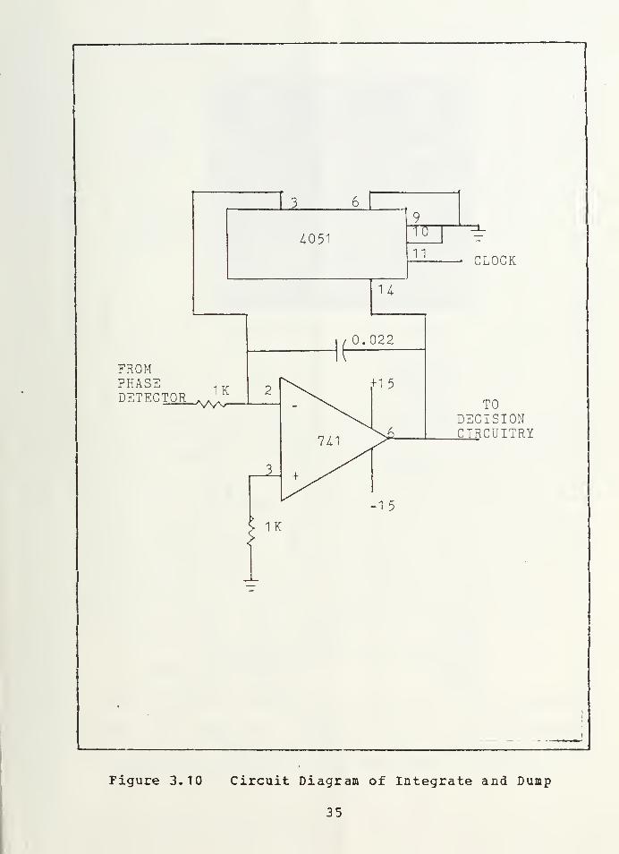
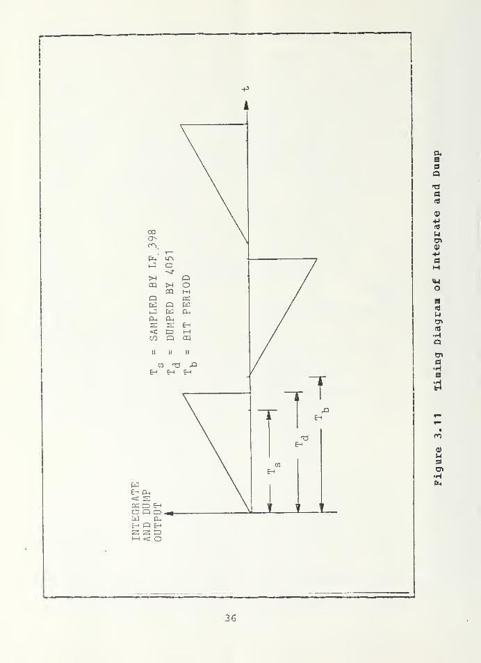
B. INTEGRATE AND DUMP
The integrate and dump circuitry is widely used to
improve noise performance of receivers used in digital data
systems. The circuitry integrates the demodulated signal
over a symbol interval. At the end of the interval, the
integrator output is sampled just prior to "dumping" or
returning to zero. This reduces the effect of the noise and
presents a peak value which can be used as the input to a
sample and hold circuit. The two components used in the
integrate and dump circuitry are the multiplexer 4051 and a
741 op-amp. The circuit is shown in Figure 3.10. The inte-
grate and dump circuitry integrates the incoming signal and
then returns to zero voltage (dumps) when the feedback
circuit is shorted by the multiplexer. The clock signal
which triggers the multiplexer is timed so that the dump
occurs just before a new three bit block of data is trans-
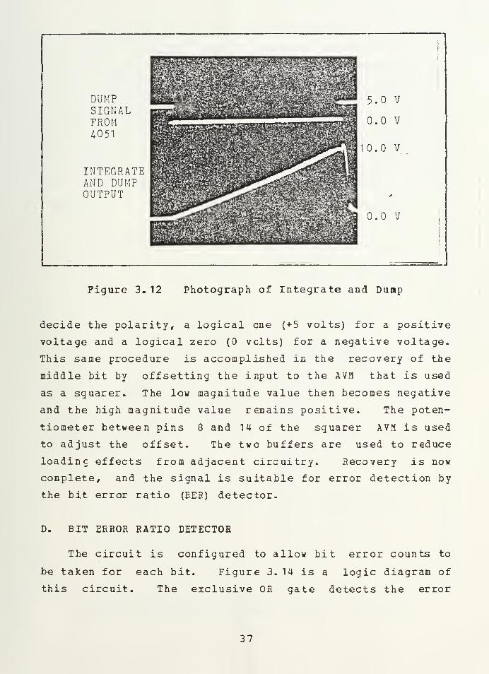
mitted. A timing diagram is shown in Figure 3.11. A photo-
graph of the output of the integrate and dump circuitry is
included in Figure 3.12. In Figure 3.12 the upper waveform
on the photograph is the dump signal and the lower waveform
indicates the output of a complete integrate and dump cycle.
The output of the integrate and dump circuitry is a positive
or a negative voltage which is translated into a logical one
or zero in the next stage.
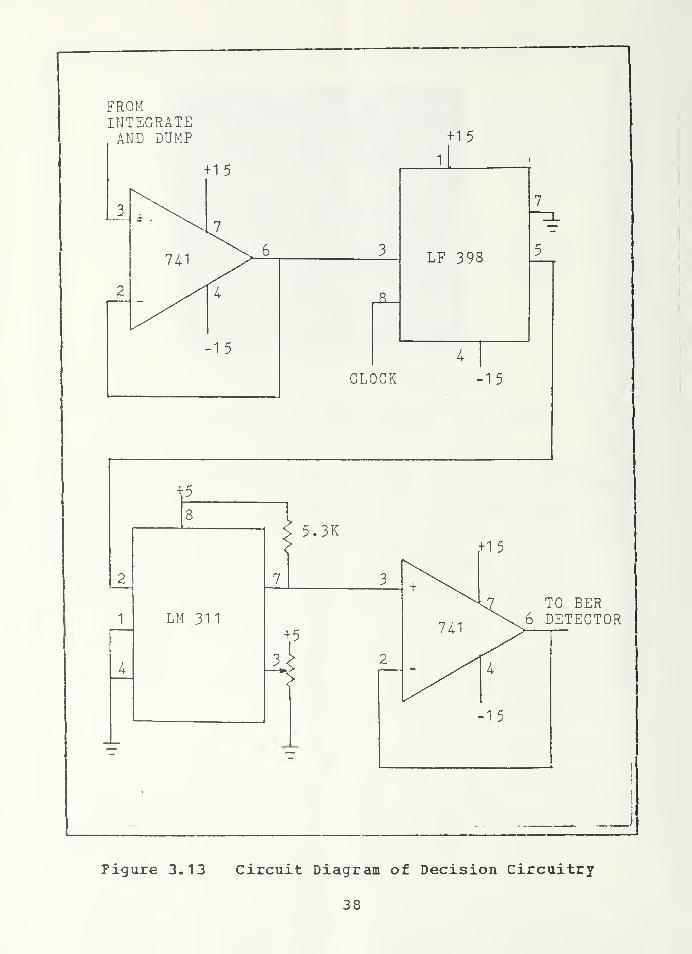
C. DECISION CIBCDITBY
The decision circuitry is composed of a sample and hold
device (IF 398), a comparator (1M 3 11), and two buffers (741
op-amps). Figure 3.13 shows the decision circuitry. The
clock for the the sample and hold device is designed to
sample just before the dump portion of the previous circuit.
Therefore, the desired value (the output of the integrate
and dump circuit) is sampled just before its peak value and
is held for the comparator. The comparator is used to
34
FROMPHASEDETECTOR 1K
vw-
40511
11
}{
U
0.022
I1K
-15
CLOCK
TODECISIONCIRCUITRY
Figure 3.10 Circuit Diagram of Integrate and Dump
35
-p
A
COOrr
>.
fe UT\
J O>H oPQ >H o
m h-l
Q cr;
W Q Hi-q w OhOh P-.
s 21 ^< ^ I—
i
CO Q PQ
n II II
q t: ^3E-< E-< en
a.ada•da(d
a>
(0
M
O
a
M
•HQ
a•Ha
T3
WEh Pl,
EhPBS S ^3n <=C O
f I I
d>M9D»•H
36
DUMPSIGNALFROM4-051
INTEGRATEAND DUMPOUTPUT
5.0 V
0.0 V
10.0 V
0.0 V
Figure 3. 12 Photograph of Integrate and Dunp
decide the polarity, a logical one (+5 volts) for a positive
voltage and a logical zero (0 vclts) for a negative voltage.
This same procedure is accomplished in the recovery of the
middle bit by offsetting the input to the AVH that is used
as a sguarer. The low magnitude value then becomes negative
and the high magnitude value remains positive. The poten-
tiometer between pins 8 and 14 of the squarer AVM is used
to adjust the offset. The two buffers are used to reduce
loadinc effects from adjacent circuitry. Recovery is now
complete, and the signal is suitable for error detection by
the bit error ratio (BER) detector.
D. BIT ERBOR RATIO DETECTOR
The circuit is configured to allow bit error counts to
be taken for each bit. Figure 3. 14 is a logic diagram of
this circuit. The exclusive OR gate detects the error
37
FROMINTEGRATEAND DUMP
+ 15
-15
+ 5
LM 311
+ 15
LF 398
CLOCK -15
5.3K
+.5
+15
TO BER6 DETECTOR
-15
Figure 3.13 Circuit Diagram of Decision Circuitry
38
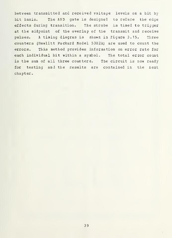
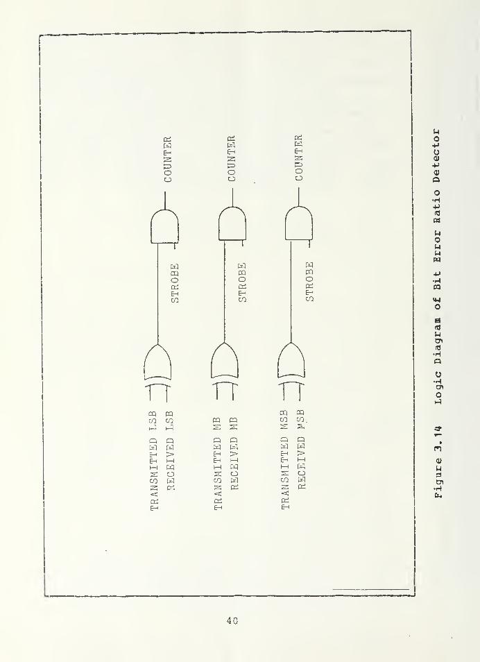
between transmitted and received voltage levels on a bit by
bit basis. The AND gate is designed to reduce the edge
effects during transition. The strobe is timed to trigger
at the midpoint of the overlap of the transmit and receive
pulses. A timing diagram is shown in Figure 3.15. Three
counters (Hewlitt Packard Model 5302A) are used to count the
errors. This method provides information on error rate for
each individual bit within a symbol. The total error count
is the sum of all three counters. The circuit is now ready
for testing and the results are contained in the next
chapter.
39
os tf os
H w wE-h &H Eh
!3 s SC3 & 1=3
O o OO o o
wPQoOSE-t
CO
WPQOOSE-i
CO
WPQOpsEhCO
oPo<u-p
<1>
Qo•H•M(0
a(-1
oMMW
•P•HCQ
*M
a«j
WCn(fl
•HQU•H
o
PQ PQ PQ PQ
CO CO PQ PQ CO CO
H-3 J S s S 5^
Q Q O O O OH H H H H WFh > Eh > Eh >Fh n Eh M Eh 1—
I
1—
1
W 1—
1
H 1—
1
wS o IS o S oCO W CO w CO ws OS 525 PS 3 PS
< <H <OS PS PSEh Eh Eh
»
0)
M
en
40
TRANSMITTEDDATA
I i
T, = TIME TRANSMITTED BIT READY
H"RECEIVED
DATA T = TIME RECEIVED BIT READYr
-I
BERDETECTOR —JT U— T
g= STROBE
i
I
i
i
1 1 i
|» T,k -I
Tk
= TRANSMISSION DELAY TIME
T = OVERLAP TIMEP
Figure 3. 15 Timing Diagram cf Bit Error Ratio Detector
41
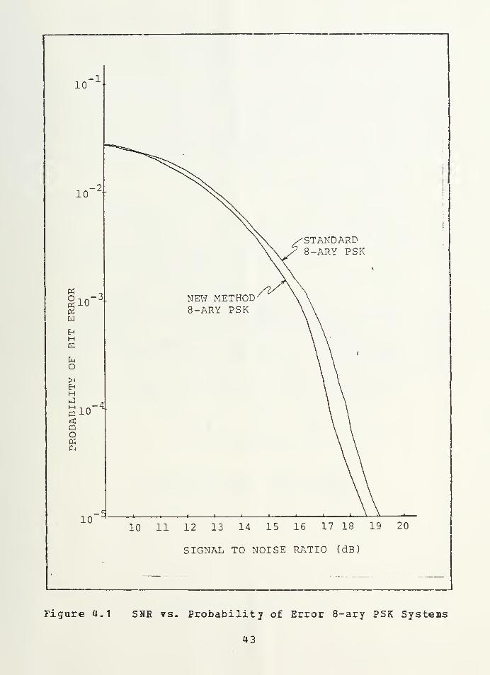
IV. RESOLTS AND CONCLUSIONS
The results of the testing of this communications system
are compared with experimental results of 8-ary PSK. The
signal to noise ratio (SNR) in dB versus the probability of
error curves are shown in Figure 4.1.
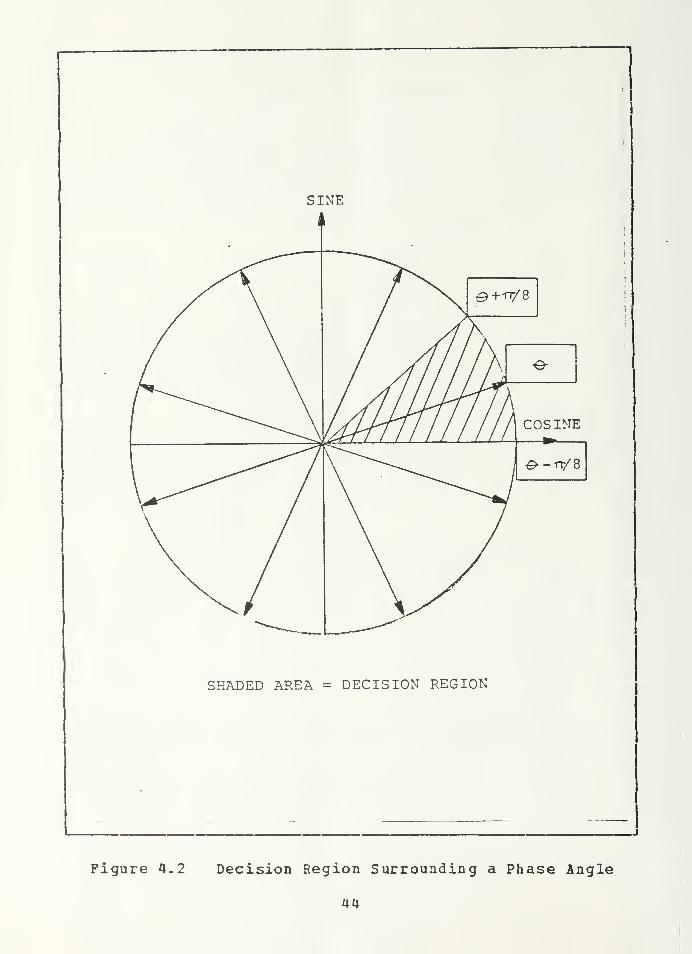
A. THEORY
The standard values for 8-ary PSK are given in many
communications textbooks and are called the "waterfall
curves" (SNR vs. Probability of Error) . These waterfall
curves can be used to compare different communications
systems. The analysis of finding the probability of error
for 8-ary PSK uses the phasor diagram in Figure 1.1. A
decision region is established around each phase angle [-0-)
as shown in Figure 4.2. Thus a decision error is made if
the noise causes the phase to fall outside of the range
Q— tt/8 < €><€+ rr/8
This is the method adopted by mcst textbooks [Ref- 3]. This
analysis assumes that the receiver consists of eight phase
detectors and that the decision logic selects the phase
detector with the largest outjut. Probability of error
curves which are based on this analysis then cannot be
compared with receivers that use two phase detectors such as
the one tested in this report. Further, the decision logic
in this receiver decodes all three bits simultaneously and a
decision matrix is not necessary to recover the data bits.
These differences will affect the probability of error anal-
ysis which is a topic for further study.
42
10-1
io-2t
gio" 3
WEhHHfMOXEh
310<O
-4.
10_c
STANDARD8-ARY PSK
NEW METHOD8-ARY PSK
10 11 12 13 14 15 16 17 18 19 20
SIGNAL TO NOISE RATIO (dB)
Figure 4.1 SNE vs. Probability of Error 8-ary PSK Systems
43
SINE
1
1
e+"<V8
-e-
COS INE
-©-1T/8
SHADED AREA = DECISION REGION
Figure 4.2 Decision Region Surrounding a Phase Angle
B. STANDARD 8-ARY PSK
To compare the results of this study with standard 8-ary
PSK the transmitter was adjusted to transmit the phases as
shown in the phasor diagram in Figure 1.1. The phasor
diagram shows eight phases equally spaced. The receiver was
not changed except to optimize the threshold levels
resulting from the phase changes. The data for this system
is shown in Figure 4.1 foe comparison with the new modula-
tion technique.
C. RESULTS
The results of the new modulation technique are also
shown in Figure 4.1. This technique shows an improvement of
approximately 0.4 dB over conventional PSK.
D. CCNC10SIOHS
The results of the testing of this communications system
support the concept stated in the introduction. Decision
regions should be spaced equally, and because decisions are
based en voltage (not phase) , this new modulation technique
gives a measurable improvement in noise performance.
45

LIST OF REFERENCES
1. Hevlett-Packar d Company, Operating and Service ManualModel 35 75A Gain-Phase Meter7~7972.
2. McRae, John L. , Experimental Evaluation of a New Formof Quadrature Modulation IncIudTnq Design o? th"eFqduIaTor anH Demodulator # HasTer^s TEesis. NavalPostgraduate ScHooT, HonTerey, California, 1983.
3. Proakis, John G. Dig it al Communications, McGraw-HillBook Company, 1983.
4. Hamming, Richard W., Coding and Information Theory,Prentice-Hall, Inc., 1 9B"0
.
46
INITIAL DISTRIEUTION LIST
No. Copies
1. Library, Code 142 2Naval Postgraduate SchoolMonterey, California 93943
2. Department Chairman, Code 62 1
Department of Electricaland Computer EngineeringNaval Postgraduate SchoolMonterey, California 93943
3. Associate Professor Glen A. Myers, Code 62Mv 5Department of Electricaland Computer EngineeringNaval Postgraduate SchoolMonterey, California 93943
4. Assistant Professor Daniel Buk.ofzer, Code 62Bu 1
Department of Electricaland Computer EngineeringNaval Postgraduate SchoolMonterey, California 93943
5. Major Gregory E. Thompson, USMC 2Naval Electronics CommandCode 154P (ULS)Washington, D.C.
6. Defense Technical Information Center 2Cameron StationAlexandria, Virginia 22314
47

at ir


21316**
Thompson
Experimental evalual-on of a new for^ GTM-ary
(M=8) phaseShift Keying includingdesign of the trans-
S
mitter and receiver.
The sisTU332c.l
21316**
ThompsonExperimental evalua-
tion of a new form ofM-ary (M=8) PhaseShift Keying includingdesign of the trans-mitter and receiver.