Embed Size (px)
Citation preview

Chapter 2
Experimental Apparatus and Characterization
Techniques
In this chapter we discuss the experimental apparatus that was
implemented during this thesis work. We start with a review of cryogen
free low temperature-high field magnet system. Then we describe in
detail the design of the set up for rf penetration depth measurement. We
also describe the specifications of some other standard characterization
tools. Sample preparation techniques and basic characteristics of the
samples used in the study are presented.

Chapter 2 Experimental Apparatus and Characterization Techniques 32
2.1 Introduction
In this chapter we discuss the experimental apparatuses that are used and
some of them that are designed and implemented during this thesis work. The
working principle of the low temperature high magnetic field facility installed
during the course of this thesis is discussed. The main characterization
techniques include magneto-resistance, the relative rf penetration depth, and
magnetization as a function of temperature and magnetic field. They have been
described in detail. Sample preparation techniques have been briefly reviewed
and basic characterization e.g., X-ray diffraction, scanning electron microscopy
and energy dispersive X -ray spectroscopy results have also been discussed.
2.2 The cryogen free low temperature - high magnetic field
system
Temperature and magnetic field are the most crucial variables for the
entire spectrum of pure scientific research. Particularly in material science and
condensed matter physics, all characterization techniques are primarily centered
on these facilities. Studies over the widest range of temperature and magnetic
field therefore hold the key to discovering new science and functional materials.
While measurements above the room temperature can be performed by
controlled heating, most low temperature experiments are carried out using a
variety of gases, prominently nitrogen and helium, in their liquid form. The
standard method is first to liquefy the gas by mechanical means, then to transfer
it to the measurement set up, and then to vaporize it over a small volume. The
latent heat of vaporization during this process is obtained from the liquid itself
leading to further lowering of temperature of the liquid phase of the gas. The
time honored procedure involves liquid helium (2He 4), which remains a gas at

Chapter 2 Experimental Apparatus and Characterization Techniques 33
atmospheric pressure down to 4.2 K. By evaporating helium at low pressure,
temperature down to 1.5 K can be easily achieved. For generating high
magnetic field too, liquid helium is indispensable. Almost all high field
magnets routinely used in research laboratories and industry are made up of
niobium based superconductors (e.g. Nb-Ti, Nb3Sn). These materials need
cooling down to 4.2 K to achieve superconducting state and to sustain high
currents in solenoidal geometry for up to 18 T field. Therefore, the production,
supply and storage of liquid helium are the most critical infrastructure
requirement for a quality condensed matter program.
Current situation however has been discouraging on two counts. For
over ten years now American Physical Society has been predicting severe
shortage of helium gas by early 21st century. A recent study indicates that
helium reserves are fast depleting and this has resulted in large scale shortage of
helium [1] and has led to postponement of projects world over. Till the new
production plants comes up the prices are expected to be almost prohibitive.
The cost of liquefier (with reasonable throughput and longevity) and its
maintenance have skyrocketed in the recent past making it next to impossible
for small groups to conduct low temperature measurements. Fortunately, with
the advent of high wattage closed cycle refrigerators, the dependence on costly
liquid helium to carry out quality low temperature experiments is a thing of the
past. In the following, we describe here the principle and successful operation
of an entirely liquid cryogen-free low temperature high magnetic facility in our
laboratory.
2.2.1 Principle of closed cycle cryocoolers
The first patent for industrial production of liquid nitrogen by
liquefaction of atmospheric gas was filed by Carl Linde (dated July 9, 1895).
The invention was based on Joule-Thomson effect which states that any real gas
Chapter 2 Experimental Apparatus and Characterization Techniques 34
undergoes a change in temperature while traversing from a high pressure region
to low pressure region under isoenthalpic condition. The change in
temperature, whether increase or decrease, is determined by change in internal
energy of the gas when the average separation between the molecules of the gas
increases under expansion [2]. Almost 65 years later, Kohler and Jonkers at the
Philips Lab. were the first to implement a closed cycle based air liquefier,
formally known as the Philips-Sterling cycle. The cooling was achieved by free
expansion of gas rather than the throttling process of J-T effect. This was based
on compression of gas followed by transfer through a regenerator onto a space
where the gas is expanded and cooled before returning to uncompressed state.
The regenerator acts as a heat exchanger as well as a thermal seal between the
warm and cold ends. The 'Kohler' design involved out of phase movement of
two pistons with helium gas as the working substance [3]. The Gifford
McMahon (GM) cycle [4, 5] on which most of the present day sub-4 K ----cryogen-free refrigerating systems are based, is a straight forward modification
of the Philips-Sterling method.
Single stage GM cryocoolers ( ~ 30 K), have been widely used as cryo
pumps and as radiation shield in MRI machines for decades. Shown in Fig 2.1
is the schematic diagram of the GM cycle. The main parts of the GM apparatus
are, a) compressor CP, b) displacer piston D, c) regenerator R, d) intake valve
V" and e) exhaust valve VE. The working material could be pure helium gas.
The displacer is cased inside a cylinder and its basic function is to displace a
volume of gas through the thermal regenerator R. The regenerator maintains a
large thermal gradient between the cold and hot ends of the cylinder. It is made
up of materials with large molar heat capacity. The displacer is tight fitted to
the cylinder through sliding seals that prevent gas flow through the radial space
between the displacer and the cylinder. Effectively, the cold (C) and warm (W)
volumes can be varied by the movement of the displacer but the total volume
remains constant throughout the cycle. The opening and closing of the intake

Chapter 2 Experimental Apparatus and Characterization Techniques 35
and exhaust valves are synchronized with the position of the displacer in the:
cylinder through a rotary drive mechanism. The four distinct steps of the GM
cycles as depicted in Fig 2.1 are;
i) With displacer at the cold end, intake valve VI is opened and the
compressed helium gas fills the volume W.
ii) The displacer is moved to warm end with VI open. In order to keep
the pressure constant gas slowly flows into the cold volume C
through the regenerator R.
iii) The intake valve is then closed and the exhaust valve V E is opened
forcing the compressed gas at the chamber C to undergo expansion
and consequent cooling.
iv) The dis placer is moved towards the cold end to drive the remaining
gas in the volume C. The exhaust valve is closed and the cycle is
repeated.
The performance of the GM cryocooler depends to a great extent on the
effectiveness of the regenerator material. _ In conventional two stage GM
cryocoolers, usually lead (Pb) is used as regenerator and temperature down to 6
K can be achieved. However the heat capacity of lead is negligible as
compared to pressurized helium below 6 K and therefore it is impossible to
reach sub liquid helium temperatures with lead as the regenerator. Using rare
earth alloy GdxEr1_xRh, Yoshimura et al. were the first group to reach 3.3 K by
using a 3 stage GM cryocooler [6]. These compounds undergo a magnetic
ordering transition below 20 K. Here the displacer has three stages, which
means that it uses three different materials as regenerators depending on the
temperature of the stage. In the process Yoshimura et al. were able to produce
liquid helium at the rate of I 0 cc/h by condensing helium gas near the cold
head. However high price of the Rh based materials prevented large scale
commercialization of this technique.

Chapter 2 Experimental Apparatus and Characterization Techniques 36
(ii)
(iii) (iv)
v. v.
Fig 2.1: Schematic description of four stages ofGM cycle based cryocooler.
Recent development in regenerator technology has enabled the use of
Er3Ni/Er0 9 Yb0 1Ni hybrid regenerator which is cost effective and can provide
cooling power up to 1.5 W at 4.2 K [7]. Now even sub 2 K cryocoolers are
available using a variety of magnetic resonators. A typical design as described ... ~
by Numazawa et al. uses spherical Pb particles in copper mess as the first stage .,.-regenerator and a mixture of Pb, HoCu2, Gd20 2S, GdA103, and GdV04 as the
second stage regenerator [8]. Sumitomo Heavy Industry (SHI) of Japan is the
industry leader in this technology. Most of the cryogen-free high magnetic
field systems built by Janis, Cryogenics, Cryolndustries, Cryomagnet, and
Cryomech are based on SHI compressors and displacers.
Chapter 2 Experimental Apparatus and Characterization Techniques 37
2.2.2 Details of cryogen free system at JNU
The low temperature - high magnetic field facility installed at JNU can
cool down to 1.6 Kin temperature and can generate upto 8 Tesla magnetic field
without any use of liquid cryogen. With separate attachments the sample space
can be cooled to 300 mK (He3) and heated upto 1000 K (encapsulated oven).
More advanced models with hybrid magnets can produce upto 18 T field.
These models require two compressors, one for cooling the magnet and the
other for cooling the sample space.
The system that is installed at JNU is a single compressor open ended
system. It involves a SHI compressor model CS W 71 in conjunction with a two
stage displacer model SRDK 408D. The compressor is water cooled and
requires continuous supply of chilled water ( ~ 15 °C) at the rate 7 lit/min. The
3 phase power requirement is~ 9 kW. Fig 2.2 shows the sketch of the system.
The cooling powers at the first and second stage cold heads are 34 W @ 40 K
and 1 W@ 4.2 K respectively. The second stage cooling is shared between the
sample space and the Nb-Ti superconducting magnet (T c = 9 K). The first stage
is connected to an ultra pure aluminum radiation shield. The magnet is latched
to the second stage of the compressor. A condensation pot is attached to the
magnet. When low pressure helium gas from a separate close cycle reservoir is
brought in contact with condensation pot the gas liquefies and with suitable
pumping, the base temperature of 1.6 K can be achieved. It is to be emphasized
that the process is entirely liquid cryogen-free and during the run over the last
almost three years we have not spent a single rupee on consumables like liquid
nitrogen or liquid helium or helium gas. Further since the sample space is
always cooled by the helium vapor, the vibrations due to mechanical movement
of displacer hardly interfere with the measurements. Moreover, for entirely
vibration-less environment, as mandated by scanning tunneling microscope

Chapter 2 Experimental Apparatus and Characterization Techniques 38
(STM) and Andreev point contact spectroscopy (PCS) measurement, the more
advanced pulsed-tube displacer could be opted.
2.2.3 Working of the low temperature high magnetic field system
The block diagram of the cryogen-free system is shown in Fig 2. 2. The
static and dynamic pressures in the compressor are 1.7 MPa and 2.5 MPa
respectively. Compressed helium from the compressor reaches the cold head
via flexible high pressure hoses. The cold head is housed in a specially
designed cryostat chamber that shields it from outside with vacuum and layers
of radiation shield. The cryostat also includes a vertical column where the
sample is inserted using a dip-stick (variable temperature insert or VTI), a
superconducting magnet and a condensation pot. The temperature of the
superconducting magnet always remains ~ 4 K except for small variation of the
order of0.5 K during charging and discharging ofthe magnet.
The radial sample space is 30 mm and the field homogeneity in this
region is 0.09% over 10 mm. The condensation pot is connected to a separate
helium gas recycle consisting of a reservoir ( ~ 50 liter helium gas at ~ 3 psi
pressure), an air filter and a dry pump. The helium gas gets liquefied locally at
the pot and its vapor flow (and therefore the temperature) in VTI chamber is
controlled by a needle valve. To reach 1.6 K a pressure or? .JP.!J~r i.~- m~il_!_tain~d
in the VTI chamber. Controlled heating using heater of variable wattage up to
25 W near VTI base dictates the temperature of the helium vapor at the sample
space. Resistive temperature sensors are placed at various points in the cryostat
such as the first stage, shield, second stage, magnet, condensation pot, and
exchanger exhaust to continuously monitor the system parameters. By
measunng the resistance at these points temperature is measured using a
Keithley 2700 multimeter with a 10 channel scanner. --------- - ~-- - -

Chapter 2 Experimental Apparatus and Characterization Techniques 39
Temperature Scanner
Keithley - 2700
Compressor Sumitomo CSW-71
Helium reservoir
Temperature controller
Lakeshore-340
VTI pressure
Dry Pump
16 pin Connector foir sample
characterization
Air lock valve
Magnet Power Supply
SMS 120C
Sample holder
Cryostat
Fig 2.2: Block diagram of the GM cycle based cryocooler and cryostat. The primary
helium closed cycle comprises of the compressor connected to the displacer through
flexible hoses. Separate helium gas close loop consists of a low pressure helium
reservoir, a condensation pot, a needle valve and a dry pump. The position of
superconducting magnet attached to the second stage of the cold head is also shown.
The other interfaced instruments such as magnet power supply, Keithley multimeter
with scanner, and temperature controller are also shown.

Chapter 2 Experimental Apparatus and Characterization Techniques 40
Fig 2.3: Low temperature and high magnetic field :;ystem along with 8 T magnet
power supply and other tools for measurements such as resistivity, magnetoresistance,
and r_f penetration depth at SPS, JNU.
The temperature in the VTI and on the sample holder is measured and
controlled by Cernox sensors using a Lakeshore 340 temperature controller.
The Magnet power supply is cryogenic Model SMS 120 C. The maximum field
of 8 Tesla requires current flow of I 08 Ampere. The magnet is fitted with a
persistent switch that enables very stable homogeneous field.
The fi rst cool down of the system from room temperature to the base
temperature takes about ~ 12 hours. At the base temperature, second stage,
magnet, and condensation pot maintain ~ 4 K where as first stage, shield, and
exchange exhaust remain at around ~ 37 K. At this point helium from second
closed loop is allowed to flow through the sample space via the condensation

Chapter 2 Experimental Apparatus and Characterization Techniques 41
pot at a pressure of~ 8 mbar. The He pressure can be controlled by the needle
valve, and at 8 mbar, the temperature goes down to 1.6 K in ~ 2 hour. An
advantageous feature of this system is that sample under test can be taken out of
the system without warming the system to room temperature (unlike the
Quantum Design PPMS). This is achieved by an airlock valve. Further, we
have the flexibility to design the attachments based on our requirements.
Measurement of de and ac resistivity, Hall effect, magneto-resistance needs
little modification to the sample holder as supplied by the manufacturer.
Attachments for measuring rf penetration depth and dielectric constant have
been designed and implemented at JNU. Evidently, the experimental data
quality is not compromised in spite of the mechanical movement of the piston
and due to the varying heat load during the isofield temperature scan.
2.2.4 Attachments for various measurements
Some of the attachments designed for cryogen free low temperature and
high magnetic field system are shown below in the Fig 2.4. Depicted in Fig 2.4
(a) is LC tank circuit, that is part of rf penetration depth measurement setup.
The coil and capacitor attached to sample holder are shown. Coil was wound
tightly on a teflon mantel and was put inside a G-1 0 coil holder. This was then
attached to the sample holder. Teflon mantel helps the coil in adopting uniform
shrinkage at low temperature. Fig 2.4 (b) shows the attachment for dielectric
constant measurement. It is derived from capacitance. Sample is sandwiched
between copper electrodes placed on specially designed G-1 0 plates. The
movement of these plates is controlled by springs. The attachment is then
screwed to the sample holder. The temperature sensor on the sample holder is
also visible in this figure.

Chapter 2 Experimental Apparatus and Characterization Techniques 42
"
Capacitor [C] Coi l [L]
Fig 2.4: (a) Attachment for LC tank circuit that is part of 1.[ p enetration depth
measurement setup.
Fig 2.4: (b) Attachmentfor capacitor measurement is depicted. Sample can be placed
between the copper electrodes. The tight fitting of electrodes is controlled by .springs.

Chapter 2 Experimental Apparatus and Characterization Techniques 43
2.3 Linear four probe technique for resistivity measurement
For resistivity measurement we used linear four probe technique. Four
contact points situated linearly are taken out from the sample and a known
current from a current source (Keithley 2400/Keithley 224) is made, to pass
through the outer tabs, and potential drop across inner tabs is measured through
a voltmeter (Keithley 2182 nano-voltmeter). DC voltage with resolution~ 50
nano-Volt has been achieved with the GM compressor running. Resistivity is
derived from resistance thus measured by determining the area of cross section
and the thickness of the sample. The contacts on the sample were deposited
using conducting silver paint. For magneto-resistance we applied the field in a
direction always orthogonal to the current direction.
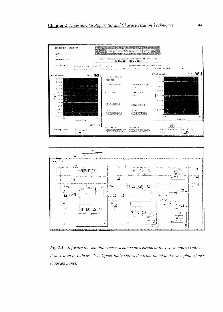
2.4 Interfacing software
Instruments used in the experiments e.g. Lakeshore 340 temperature
controller, Keithley 224 current source, Keithley 2400 source meter, Keithley
2182 dual channel nano-voltmeter, Keithley 2000 digital multimeter, Agilent
5 3131 A frequency counter, SMS 120 C cryogenic magnet power supply, and
Stanford Research System SR530 lock in amplifier were all interfaced and the
data acquisition was controlled by a computer. The program for interfacing
these machines is written in the Labview 6.1 software. One such software for
resistance measurement for two samples simultaneously is shown in the Fig 2.5.
The first figure depicts the front panel of the program while the second figure
shows the arrangement of various Labview components.
Chapter 2 Exrerimental Arrwratus and Characterization Techniques 44
J-:-'
~~~ I
w .. ;;E
f
·~~-I ~
- :1
Fig 2.5: Sofhmrej(Jr simultaneous resistance measurementfor tHD samples is sh•n\'11.
It is Hritten in Lahvinr 6. I. Cpper plate shows theji-ont panel and lo'>t·er plate .\l'ows
diagram panel.

Chapter 2 Experimental Apparatus and Characterization Techniques 45
2.5 Radio frequency penetration depth setup
2.5.1 The technique
Several techniques are available for penetration depth measurement such
as pSR, microwave surface impedance, and small angle neutron scattering
(SANS) [9-12]. The simplest yet the time honored technique is the tunnel diode
oscillator technique. Tunnel diodes are almost obsolete but for this interesting
application. This technique is based on a highly stable tunnel diode (BD-4)
based radio frequency oscillator that includes a LC tank circuit. The sample is
placed inside the inductor of the tank circuit. The LC part is attached to the low
temperature facility to access temperature down to 1.6 K and field up to 8
Tesla. The effective change in the rf penetration depth is measured as shift in
frequency of the oscillator using an ultra-stable frequency counter.
In this type of LC oscillators, the tunnel diode is biased in negative
resistance region, and acts as a power source to overcome the losses in the
Ohmic, inductive and capacitive components. The main component of a tunnel
diode is a narrow (~100 °A), heavily doped p-njunction. Shown in Fig 2.7 is a
measured 1-V characteristic of this diode that prominently features a negative
resistance region. Once the oscillations set in, an rf current at the resonant
frequency flows in the inductor of the tank circuit and a corresponding rf
magnetic field is generated. This flux penetrates the sample kept in the coil and
depending on the magnetic state of the sample, the effective area allowed for
the flux through the inductor changes. The corresponding change in the
frequency of the oscillator thus accurately reflects the magnetization state of the
sample. In case of superconductors, as the temperature goes below the
transition temperature, the flux is expelled due to the ensuing diamagnetic state.
This leads to decrease in L and an increase in resonant frequency of the

Chapter 2 Experimental Apparatus and Characterization Techniques 46
oscillator. The magnitude of the shift in frequency is proportional to sample
density and geometry.
Schawlow and Devlin [13] were amongst the first to present the
apparatus to accurately measure the change in penetration depth using oscillator
technique. We know that the self inductance L of a solenoid depends purely on
geometrical parameters (L = ~0 n nr2, n is the number of turns per unit length).
As the temperature is decreased, along with a contribution from the
magnetization state of the sample, the inductance can also change because of
shrinking coil diameter and length. Therefore a proper background subtraction
is important for quantitative determination of penetration depth. For a coil of
inductance L and radius r of the sample, let A be the cross-sectional area
occupied by the flux. The change in penetration depth with the change in the
inductance of the coil will then be;
L\L/L= L\ A 2m/ A
In terms of oscillator frequency (since F2
depth can be written as
L\ A= (A/m) (L\F/F) = GL\F
(2.1)
1 /LC), the change in penetration
(2.2)
where G is a calibration constant that depends on sample and coil geometry.
Thus, the shift in oscillator frequency L\F is proportional to the change in
penetration depth L\A.
The value of G can be determined by using a specimen with known radio
frequency skin depth. We used oxygen free high purity copper for the
calibration. The specimen geometry and its orientation inside the coil was
made similar to the actual superconducting samples under study. However, our
Chapter 2 Experimental Apparatus and Characterization Techniques 47
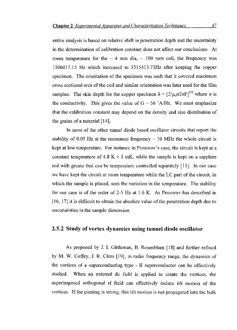
entire analysis is based on relative shift in penetration depth and the uncertainty
in the determination of calibration constant does not affect our conclusions. At
room temperature for the ~ 4 mm dia, ~ 1 00 tum coil, the frequency was
1506017.15 Hz which increased to 1515413. 73Hz after keeping the copper
specimen. The orientation of the specimen was such that it covered maximum
cross sectional area of the coil and similar orientation was later used for the film
samples. The skin depth for the copper specimen 8 = [2/ Jl0 cr2nF] 112 where a is
the conductivity. This gives the value of G ~56 OA/Hz. We must emphasize
that the calibration constant may depend on the density and size distribution of
the grains of a material [ 14].
In most of the other tunnel diode based oscillator circuits that report the
stability of 0.05 Hz at the resonance frequency ~ 10 MHz the whole circuit is
kept at low temperature. For instance in Prozorov's case, the circuit is kept at a
constant temperature of 4.8 K ± 1 mK, while the sample is kept on a sapphire
rod with grease that can be temperature controlled separately [15]. In our case
we have kept the circuit at room temperature while the LC part of the circuit, in
which the sample is placed, sees the variation in the temperature. The stability
for our case is of the order of 2-5 Hz at 1.6 K. As Prozorov has described in
[16, 17] it is difficult to obtain the absolute value of the penetration depth due to
uncertainties in the sample dimension.
2.5.2 Study of vortex dynamics using tunnel diode oscillator
As proposed by J. I. Gittleman, B. Rosenblum [ 18] and further refined
by M. W. Coffey, J. R. Clem [19], in radio frequency range, the dynamics of
the vortices of a superconducting type - II superconductor can be effectively
studied. When an external de field is applied to create the vortices, the
superimposed orthogonal rf field can effectively induce tilt motion of the
vortices. If the pinning is strong, this tilt motion is not propagated into the bulk

Chapter 2 Experimental Apparatus and Characterization Techniques 48
and is confined only to the surface. In the other extreme, under negligible
pinning, the oscillating vortices can permeate the entire sample. This is shown
in Fig 2.6. Thus the rf penetration depth becomes a true measure of bulk
pinning force density. At high fields one can also access the flux flow regime
using this technique. As defined in Eq. 1.2, the vortex displacement can be
written as kpu + 11(du/dt) = Jx~o where u is the instantaneous displacement
from the vortex from its equilibrium position, 11 is the viscous drag coefficient
and kp is the restoring force constant of the pinning potential also termed as
Labush Parameter or pinning force constant. On solving above equation in the
dilute limit of flux density and periodic pinning potential, the rf penetration
depth can be written as [19]
(2.4)
2 . ~ where 'Ac = B~o/11-okp defines the Campbell penetratiOn depth and 'At =
2B~ol!l-o11CO defines the flux flow penetration depth. Thus with isothermal fi.eld
dependent measurement of rf penetration depth, one can access information
about pinning force density and coefficient of viscosity in the flux flow regime.
t Hdc~ X Hac ~
~A.=O
Strong pinning
Medium pinning
~~~. = 00
Weak pinning
Fig 2.6: Shift in rf field penetration depends on the strength of flux pinning.

Chapter 2 Experimental Apparatus and Characterization Techniques 49
2.5.3 Design of the oscillator circuit
The paper by C. Boghosian, H. Meyer, and J. E. Rives in 1966 is the first
published report of tunnel diode oscillator used for measurements in low
temperature physics [20]. Stability of the oscillator's resonant frequency is the
key for this technique. There are many reports on designing the tunnel diode
based ultra stable oscillator [21-26]. Though concept of basic circuit remains
same, optimizing the circuit is non trivial. The main component of the circuit,
i.e. tunnel diode is the biggest hurdle, it is tough to find but easy to bum. We
could find tunnel diode BD-4 but we lost 2 of them during the testing of the
circuit.
50
40
-30 ~ -
20
10
0 0 0 0 0 0 0 0 0 0 0 0 6 0 6 0 0 I
9
25 50 75 100 125 150 175 200 V(mV)
Fig 2. 7: Room temperature 1-V characteristics of tunnel diode BD-4 used in the
oscillator circuit. The value of negative resistance is ~2 kQ and the maximum current
is~ 55 ;d.

Chapter 2 Experimental Apparatus and Characterization Techniques 50
Shown in Fig 2.7 is the current-voltage (1-V) characteristic of the tunnel
diode used in the circuit. From 0 to ~ 40 m V, current increases. Beyond 40
m V current decreases and the negative resistance region sets in. The tunnel
diode is biased in this region. Post a series of optimization, the circuit and the
value of the components are as given below.
C3
TDBD-4
R2
C2
c
+9V
MAR SA
Inductor Ll
800mV
Out put frequency
Fig 2.8: Figure shows the design of the tunnel diode circuit with the components. The
values of the optimized components are L1 = 0.1mH, R1= 4. 7 kQ, C1 = 10 pF, R2 =
686 Q, C2 = 680 pF, C = 120 pF, R3 = 220 Q, C3 = 68 pF. The microwave amplifier
MAR 8-Afor amplification of output voltage is also shown in the circuit.
Frequency is measured by an Agilent frequency counter 5 3131 A. Since
the minimum trigger voltage of 53131A is 50 mV, we sought to amplifY the

Chapter 2 Experimental Apparatus and Characterization Techniques 5.[
oscillator signal (~ 35 mV) by using a microwave amplifier MAR-8A. The
circuit for amplifier is shown in Fig 2.9. To remove the persistent grounding
problem a printed circuit board was specially designed and the entire circuit
was kept inside a grounded metal box to shield it from external electromagnetic
interference.
IOOohm
Q--i Vee =+9V
1-----0 473nF
MAR- 8A
Fig 2.9: The design along with the values of the components for biasing the amplifier
MAR-8A.
After optimizing the oscillator circuit at room temperature it was
optimized in low temperature and high magnetic field environment. Due to
constraints in sample space, only LC tank circuit was attached to the VTI and
the rest of the circuit was kept at room temperature. This required addition of
cable of length ~ 2 meter. We found the stability to be least compromised with
semi rigid co-axial cable RG 176. Optimization of inductance of the LC tank
circuit was also carried out to improve the stability of oscillator. Initially
copper wire on top of cigarette paper was tightly wound but it was found that
while decreasing the temperature the change in the frequency was not uniform
and this could have been caused by uneven decrease in the cross sectional area
of the coil. So we decided to wrap the coil on some thin walled teflon tube. A
tube of 1 mm thickness and 3.5 mm inner diameter was chosen. Around 70

Chapter 2 Exrerilntal Armaratus and Characterization Techniques 52
turns of the 42 gauge copper wire were tightly wound (single layer) on the
Teflon tube and soaked in GE varnish to give strength to the coil. A coil holder
of G-1 0 material was designed and coil was glued permanently with GE
varnish. The coil holder is attached to the sample holder of the VTI by a set of
lmm screws. The 120 pf capacitor that forms a part of the tank circuit is
soldered to the inductor and as mentioned above, only the tank circuit is
exposed to low temperature.
The sample inside the coil can be kept in two position. The c- axis of the
sample parallel to the coil axis (that is also the direction ofHrr), and ab plane of
the sample parallel to the coil axis. The sample is placed on a notch of a
wooden cylinder that is inserted into the coil after wrapping it with teflon tape.
The circuit stability was found to be 2-5Hz at 2.34 MHz and 1.6 K for a typical
time interval of 1 0 min. It is important to note that the ac probe fidd in our
system is of the order of l~T. Fig 2.10 shows the block diagram of the
penetration depth measurement system
2.5.4 Frequency stability of tunnel diode oscillator
Fig 2.11 (a) shows the stability of the tunnel diode circuit (without
MAR-8A amplifier) at room temperature with respect to time for approximately
6 hours. The data are taken using a Tektronix oscilloscope. The figure shows
drift in frequency in the range of± 50 Hz. Fig 2.11 (b) on the other hand shows
the stability of the circuit after including the amplifier. As elucidated,, a
stability of ± 5 Hz could be achieved.

Chapter 2 Experimental Apparatus and Characterization Techniques
]~-------·
Sample inside the LC tank circuit
placed in cryogen free system
BD-4 J Frequency based counter
oscillator 1---- Agilent 53131A
Temperature controller Lakeshore
340
r---
Labview interfaced
Data acquisition Computer
53
Fig 2.10: Block diagram for the rf penetration depth measurement, only the sample
kept in the coil of LC part of tunnel diode oscillator is inside the low temperature high
magnetic field system. The temperature controller, frequency counter are connected to
Labview interfaced computer for data acquisition system.
The variation in the frequency without any sample with respect to externally
applied field was also taken. The data taken at 35 K are presented in Fig 2.12.
A variation in the frequency is ~ 40 Hz up to DC magnetic field of strength 2.5
T is observed. It is to be noted that this is negligible compared to the actual
change in signal in the presence of the sample.

Chapter 2 Experimental Apparatus and Characterization Techniques
-N :I: u: <I
-75~------------~~-----~------------~----------._-----~-----~ 0 100 200
Time (min) 300 400
10~--~-.--~---r--~--~.--~-.--~---.-,-,
-5 0
odb --10L---~~~~~---i~---~~--~--~.~~~--_.--~
0 20 40 60 80 100 Time (min)
54
Fig 2.11: Room temperature stability of the circuit (a) without using the amplifier and
(b) with using microwave amplifier MAR-8A.
500r---~--~.--~--T---T---T-,--~--r-.--~--.
400 -
300 f-
-N :I: -LL 200 f-<l
100 f- -
oooooooooooooo oooo
0 ~oooooooooooO -I i
0 5000 10000 15000 20000 25000
H (G)
Fig 2.12: Variation in the frequency with respect to the DC magnetic field at 30 K.

Chapter 2 Experimental Apparatus and Characterization Techniques 55
Tunnel diode oscillator is an extremely sensitive measurement technique
and resolution up to 1 o A has been reported. However it is also extremely
susceptible to external noise and interference. Craig T. Van Degrift who
perfected this technique, has discussed the possible sources of noise and about
the measures to reduce them [22]. Shielding and proper isolation is of prime
importance. To quote VanDegrift, "when using the tunnel diode oscillator in
Helium dewar and if it is not properly shielded then just running a hair drier can
alter the frequency of the system". In our case it is assumed that noise due to
running of close cycle compressor and other necessary machines such as UPS,
water chiller would be taken care of by the excellent radiation shielding of the
cryostat. Nevertheless, if the rest of circuit components could be placed in the
sample space, one would expect a substantial increase in stability.
2.6 Miscellaneous instruments
For the magnetization study of MgB2 thin film we used a MPMS - 5
system at the Technical Physics and Prototype Engineering Division, Bhabha
Atomic Research Center, Mumbai. The magnetic property measurement
system (MPMS) from Quantum Design is a Superconducting Quantum
Interference Device that can measure magnetization of the order of 10-7 emu.
For the structural analysis of bulk samples, we used a Bruker D-8 Advance
Diffractometer at Indian Institute of Technology, New Delhi and at the Inter
University Accelerator Center, New Delhi. For thin film XRD, we used the
facility at National Physical Laboratory, New Delhi. Both these diffractometers
have Cu Ka target with wave length 1.5418 ° A. The scanning electron
micrograph of the surface morphology is taken in a Leo 435VP Surface electron
microscope with EDAX attachment at AIIMS. The electron dispersive X-ray
spectroscopy (EDAX) attachment in the SEM is an additional tool to identify

Chapter 2 Experimental Apparatus and Characterization Techniques 56
the chemical composition of the samples. The EDAX attachment sensor at
AIIMS is primarily suited for heavier ions and can only identify the element
ranging between N a to U. So in the case of MgB2 it was not much useful.
2. 7 MgB2 thin film sample preparation
Thin film superconductors are required for practically all applications
involving superconducting electronics. After the discovery of
superconductivity in MgB2 at 39 K, various groups involved in the
superconductivity research world wide started working on the preparation of
MgB2 thin films [27]. So far various techniques have been developed for
preparation of MgB2 thin films that fall in two broad categories. These are
1. Ex-situ MgB2 film growth
2. In-situ MgB2 film growth
Ex-situ film growth involves the deposition of boron precursor film on a
substrate. This boron precursor film is then annealed in the magnesium vapor
at a suitable temperature. In the in situ growth process, the deposition of boron
is carried out followed by magnesium and the annealing is done usually in the
deposition chamber. Magnesium layer is deposited either by co-deposition, or
producing the magnesium vapor locally close to the boron film. The In-situ
growth process is favored for application where junctions are required on the
film. The best quality MgB2 films are prepared by in-situ hybrid physical
chemical vapor deposition (HPCVD) technique. Volatile nature of magnesium
does not favor the direct deposition of film by MgB2 target as it results in
magnesium deficiency [28]. This deficiency again requires the annealing in
magnesium vapor and in this process quality of the film is compromised. The

Chapter 2 Experimental Apparatus and Characterization Techniques 57
boron precursor film can be deposited by using various available techniques
such as rf magnetron sputtering, pulse laser deposition, molecular beam and
electron beam epitaxial growth, and hybrid physical chemical vapor deposition
techniques.
2.7.1 Role ofMg vapor in the preparation ofMgB2 phase
The ex-situ two-step process is the most commonly followed technique
for MgB2 thin film growth. The technique seems straight forward but it is
reasonably tricky as it involves maintaining the correct Mg vapor for high
quality films. The steps include,
a. Deposition of a boron film unto an appropriate substrate.
b. Sealing the boron precursor film and magnesium lump inside
a niobium or tantalum tube.
c. The Nb/Ta tube is then put inside a quartz ampoule that is
sealed under few mbar of high purity argon gas.
d. The ampoule is then heated up to 900 °C. The vapor pressure
ofMg plays a significant role for the correct phase formation.
S. I. Lee's group from Pohang, Korea was one of the first to report the
ex-situ process for thin film MgB2 [29]. In this process a precursor thin film of
boron was prepared followed by heat treatment in Mg vapor inside a Ta tube.
The heat treatment was carried out in an evacuated quartz ampoule to prevent
oxidation of the Ta tube. The sintering procedure included fast heating to 900
oc and holding at this temperature for 10 to 30 min followed by rapid
quenching to room temperature. Films of 400 nm thickness were grown.
Almost at the same time C. B. Eom et al. reported [30] MgB2 films prepared by
pulsed laser deposition at room temperature. They used 111 oriented single
Chapter 2 Experimental Apparatus and Characterization Techniques 58
crystal SrTi03 substrates and deposited from MgB2 targets. The base pressure
Of the chamber before deposition WaS 3 X 1 o-S mbar, and depositiOn took place
under 3 x 1 o-3 mbar of Argon. As prepared MgB2 films were post annealed in
presence of magnesium. The thickness of the film was ~ 500 nm.
Paranthaman et al. followed a similar route where in boron films on
Alz03 single-crystal substrates were deposited by electron-beam evaporation
technique at room temperature and at a chamber pressure of~ 1 x 1 o-6 mbar [31].
These 5000 to 6000 ° A thick shiny amorphous boron films were sandwiched
between cold-pressed MgB2 pellets, along with excess Mg turnings, and packed
inside a crimped tantalum cylinder. The sealed tantalum cylinder containing
the precursor film was put into a quartz tube which was then evacuated to ~
1 x 1 o-5 mbar, and sealed. The sealed quartz capsule was heated rapidly to 600
°C, and maintained there for 5 minutes. Then, the furnace temperature was
rapidly increased to 890 °C, and held there for 10 to 20 minute, and then cooled
to room temperature. The as formed purplish gray film had a low two probe
resistance of - 1 Q. The MgB2 phase was confirmed by XRD analysis.
Similarly, S. R. Shinde et al. used pulsed laser deposition for boron precursor
film that was sintered in Mg vapor at 900 °C [32]. The boron films were
deposited at 800 °C on SrTi03 (100) and (111) substrates. The background
pressure was below ~ 10-7 mbar. In fact, small Mg balls were found to be
sticking on the film surface after the ex situ reaction in Mg vapor. This excess
Mg was removed by evaporation or by selective etching, without affecting the
underlying film properties. S. H. Moon et al. on the other hand wrapped the
boron films together with magnesium pieces and several pieces of titanium in a
tantalum foil [33]. Titanium pieces prevented the direct contact of the boron
film to the tantalum foil. Then, this whole thing was encapsulated in a quartz
tube. To find an optimum annealing condition, Moon et al. have varied the
annealing temperature and annealing time. The thickness of thin films
increased about 70% to 80% due to the annealing. S.D. Bu et al. have reported
Chapter 2 Experimental Apparatus and Characterization Techniques 59
the preparation of MgB2 thin films by depositing boron precursor film via RF
magnetron sputtering, followed by a post deposition anneal at 850 oc in the
presence of magnesium vapor [34]. Two different epitaxial MgB2 thin films on
(000 1) Ah03 were reported. The base pressure before boron deposition was
3x10⁻⁶ mbar. Deposition was carried out at 5x10⁻³ mbar Argon at 500 oc using
a pure boron target. The thickness of the boron films was 230 nm. The films
were annealed in an evacuated quartz tube using a tantalum envelope. The
quartz tube was filled with - 7-10 mbar of Argon gas after evacuation to reduce
the magnesium loss. One of these films showed extremely high upper critical
field [35].
Similarly A. Plecenik et al. deposited boron thin films by thermal
evaporation on unheated sapphire substrates and, subsequently enclosed it in a
niobium tube together with magnesium tunings [36]. Boron films were
deposited on a 1x1 cm2 Al20 3 (0001) substrate by electron-beam evaporation at
room temperature with a thickness of about 300 nm. For post annealing under
magnesium vapor, the as deposited boron films were wrapped in tantalum foil
with magnesium lumps followed by encapsulation in a quartz tube containing
high purity Argon gas. The base pressure inside the quartz tube was maintained
below 5x 10·5 mbar and the Argon pressure was set to 60 mbar. The
encapsulated samples were annealed at 800 oc with the annealing time varied
from 1 minute to 30 minute.
Kenji Ueda and Michio Naito have reported [37] the in-situ synthesis of
as grown superconducting thin films of MgB2 using molecular beam epitaxy
(MBE). They obtained as grown superconducting films in a limited growth
temperature range of 150 to 320 oc_ At such low temperatures, films are poorly
crystallized but showed a sharp superconducting transition Tc at 36 K. The use
of a higher growth temperature to improve the crystallinity failed because the
magnesium in the films was completely lost. Films were grown on various
substrates SrTi03 (00 1 ), r- Al20 3, c- Ab03, and Si (111 ). In specially designed

Chapter 2 Experimental Apparatus and Characterization Techniques 60
MBE chamber base pressure was ~ 1-2x 1 o-9 mbar. The flux ratio of
magnesium to boron varied from 1.3 to 1 0 times higher compared to the
nominal flux ratio. The growth rate was 2-3 ° A/s, and the film thickness was
typically around 1 00 nm.
X. X. Xi's group at Penn State University, USA [38] has reported a new
method for fabrication of high quality MgB2 film by in-situ hybrid physical
chemical vapor deposition technique. In their experiment they placed a
substrate on a plate, temperature of which can be raised separately. The
magnesium vapors are created by heating the magnesium chips placed around
the substrate. Further, pure nitrogen is used followed by hydrogen, and the
magnesium chips are heated to 700 °C. Small amount of diborane (B2H6) is
then added to the hydrogen flow, and a stoichiometric MgB2 deposits on the
substrate. Switching off the diborane supply terminates the film deposition.
The high hydrogen gas pressure helps in eliminating any chance of oxygen
contamination of the film, and restricts any evaporation of magnesium from the
film. Transition temperature as high as 39 K, and RRR value ·~ 80 has been
reported for such films [39].
R Vaglio et al. [ 40] has reported the in-situ preparation of MgB2 film by
modified DC magnetron sputtering system for in-situ annealing in magnesium
vapor atmosphere. They first deposited the boron precursor film on Ah03
substrate followed by in-situ annealing in magnesium vapor at 830 °C for 10
minute. The argon pressure was 9x 1 o-3 mbar during deposition while the
chamber base pressure before establishing the plasma was ~ 1 o-9 mbar. Their
best film showed the transition temperature ~ 35 K. Some other reports for the
growth ofMgB2 film by in-situ technique are listed in the reference [41, 42].
Here in this study we have tried to grow MgB2 films by following the
ex-situ technique. For the second step of annealing of precursor boron film, we
used stainless steel (ss) tube instead of the niobium or tantalum tube. In the ss
tube we kept boron precursor film and magnesium powder for annealing [43].

Chapter 2 Experimental Apparatus and Characterization Techniques 61
We have been partially successful in making the MgB2 film which showed
onset of Tc at~ 38 K, and some of them showed complete transition at~ 22 K
though the quality of the films needs further optimization.
2.7.2 RF sputtering system for thin film deposition
We have tried ex-situ RF sputtering method to grow MgB2 thin films. A
sputtering system consists of an evacuated chamber, a target holder (cathode),
and a substrate holder (anode). At the base pressure typically ~ 10-6 mbar an
inert gas typically Argon is introduced in the chamber. The electric field inside
the sputtering chamber between the electrodes is established due to the
application of rf power. This field accelerates the available ambient electrons,
and these electrons collide with Argon atoms thus producing Ar + ions as well as
more electrons and characteristic purple/blue plasma appears. These charge
particles are then accelerated by the electric field; the electrons move to the
anode and the Ar + ions move towards the cathode. When an ion approaches the
target, in the optimum conditions, this impact can start a series of collisions
between atoms of the target leading to the ejection of some target particles.
This process is known as sputtering. Particles ejected in this process are useful
and when they strike the substrate they get condensed and deposited on the
surface of the substrate. A rf sputtering system allows the deposition of non
conductive materials at a practical rate [ 44]. Fig 2.13 shows the schematic
diagram of the sputtering chamber and the associated rf power supply of the
system used for thin films sample preparation at JNU. The target of diameter 1
inch can be fitted into the target electrode while substrate electrode diameter is
~ 1 0 em. For our MgB2 preparation the optimized distance between the target
and substrate was kept at 4 em. The rf generator is operated at 13.56 MHz.
The material to be sputtered is made into a target and mounted onto a circular
copper backing plate. For precursor boron film, the target consists of a circular
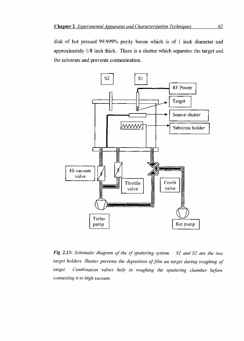
Chapter 2 Experimental Apparatus and Characterization Techniques 62
disk of hot pressed 99.999% purity boron which is of 1 inch diameter and
approximately 1/8 inch thick. There is a shutter which separates the target and
the substrate and prevents contamination.
Hi vacuum valve
Turbo pump
Throttle valve
RF Power
Source shutter
Substrate holder
Comb valve
Rot pump
Fig 2.13: Schematic diagram of the rf sputtering system. Sf and S2 are the two
target holders. Shutter prevents the deposition of film on target during roughing of
target. Combination valves help in roughing the sputtering chamber before
connecting it to high vacuum.

Chapter 2 Experimental Apparatus and Characterization Techniques 63
2. 7.3 Deposition process
The chamber is first evacuated by rotary pump before being opened to
the high vacuum turbo molecular pump. The pressure drops to below 1 o-3 mbar
(the pressure which has to be attained before the high vacuum valve can be
opened) in around 20 minutes. The time taken to reach the base pressure
(usually 5x 1 o-6 mbar here) is approximately 2.5 hours. Once the chamber is
evacuated to the base pressure, argon gas is filled in to chamber pressure of 1 o-2
mbar. Argon being a noble gas does not react with either the target or substrate.
The rf supply is then switched on and stabilized to the required power ~ 50 W
over a d.c. bias of 315 V. During this time the substrate is shielded by a shutter.
Once conditioning is complete, the shutter is opened to begin the deposition
process. We deposited the boron film on polished side of r-cut 0001 Al20 3
substrate. The substrate and target distance smaller than 4 em was deliberately
avoided, as it may initiate the back sputtering from substrate itself. These
conditions were first optimized on glass and silicon substrates. When the
brownish boron film started appearing on the glass substrate, the substrate was
then changed to Ab03. Under these conditions a series of boron films of
thickness ~ 200-300 nm were deposited. The thickness of the film was
monitored by the thickness monitor.
The as prepared boron films were annealed in the Mg vapor. We had to
undertake a lengthy optimization process for the proper MgB2 phase formation
on the precursor films. We took different amount of Mg and annealed the
boron precursor film in different ways. We got MgB2 thin films of reasonable
quality only when we annealed the boron precursor film in argon flow with the
film and Mg powder crimped in stainless steel tube. Only a Tc of 22 K has been
achieved so far and further optimization is under way.

Chapter 2 Experimental Apparatus and Characterization Techniques 64
2.8 Sample used during the present study
We have made measurements in the following set of samples.
a. A set of MgB2 films were prepared at Applied Superconductivity
Center, University of Wisconsin, Madison, by J. Giencke, C. B. Eom
using ex-situ growth process [34]. In the process boron precursor
films were grown by RF sputtering. These boron precursor films
were annealed in Mg atmosphere at ~ 900 °C. As prepared MgB2
films were used for irradiation as well as penetration depth
measurement.
b. Polycrystalline 'MgB2 was prepared at INFM, Italy by V. Braccini.
The samples were prepared by taking high purity magnesium and
boron powder in stoichiometric ratio and ground thoroughly and
palletized. These pellets were kept in out-gassed tantalum crucible
and arc welded in argon atmosphere. These were further sealed in
quartz ampoule under vacuum and heat treated at ~ 900 °C for few
hours. This has resulted in a good quality of sample with Tc = 39.2
K, resistivity at Tc = 3.5 11-n-cm and residual resistivity ratio = 14
[45].
c. Polycrystalline MgB2 samples were prepared by Ben Senkowich at
Applied Superconductivity Center, University of Wisconsin Madison
[ 46]. Commercial MgB2 powder was thoroughly ball milled. This
milled powder was pressed to form pellets which were then welded in
evacuated SS tube and was exposed to hot isostatic pressure (HIP)
processing at 1000 °C at~ 30 Kbar. The very dense and hard sample
thus processed had a Tc of38.6 K.
d. BizSrzCazCu30 10 in the form of oriented tape were prepared at
Applied Superconductivity Center, University of Wisconsin

Chapter 2 Experimental Apparatus and Characterization Techniques 6.5
Madison, by J. Jiang. Standard powder in tube process was followed.
Bi 2223 powder was filled in Ag tube which was then heat treated at
~830 oc in presence of mixture ofN2 and 0 for 2-12 hours [47].
e. Polycrystalline NbSe2 samples were prepared at the School of
Physical Sciences, JNU, New Delhi by I. Naik using solid state:
reaction technique. High purity niobium and selenium were taken in
stoichiometric ratio and ground and palletized and were heat treated
2.9 Structural analysis
Shown in Fig 2.14 is the recorded XRD pattern ofpolycrystalline MgB2
sample (INFM). No impurity is observed and all the peaks are identified.
:i 300 r::::: ::::s 0 (.) -
200
100
0 10 20
-0 0 ....... '-"
30 40
2e (degrees)
Fig 2.14: XRD pattern ofpolycrystallineMgB2.
-0 ....... -N ....... '-" 0 -0 N
'-" 0
50 60 70

Fig 2.15 (a) shows the SEM image of polycrystalline MgB 2 (IN FM) that
suggests well connected grains. Sub micron sized grains arc equally distribu1ed
in the sample. Fig 2.15 (b) shows the SEM image of unin·adiated thin film.
The grains of size less than I ~tm are uniformly distributed in the image.
Development of the minor cracks seen in the film can be attributed to the strain
developed during the film deposition.
EHT-15 00 kV Wllo 10 llll Hag, 6 25 K X Wm - Photo No ·4 Detector' SE!
Fig 2.15: SE\4 image oj(a) pol\'l.:n;stalline INF\f.V!gB:: and (h) tllin(llm o(J1gB:
Fig 2.16 shows the EDAX spectrum of polycrystalline NbSe2. High quality of
the sample is confirmed as we do not find much impurity phase in the sample.

Chaoter 2 ExQerimental AQoaratus and Characterization TechniQues
Se
Nb
l Nb • ••
1 2 3 ~ 5 8 7 6 9 Ftl ScalE! 11J'Xl6 lis CLM!or: o D[JJ
Fig 2.16: EDAX spectrum of NbSe2 polycrystalline sample.
1000
900
- 800 tn .....
700 t:: ::::s 0 600 (.) -~ 500 tn t:: Q) 400 ..... t::
300 ,........ co
200 0 0 ._
100
0 10 20
0
s
0
N S 0 0 ._
30
,........ ('(') N' ..- ..-..-..-._
40
28 (degrees) Fig 2.17: XRD pattern for Bi2Sr2Ca2Cu3010 sample.
50
s~ Sc
10 11 12
60
67
13
70
Fig 2.17 shows the XRD pattern of Bi2Sr2Ca2Cu30 10 which matches with
the standard formula Bil.84Pb0.34Sr191 Ca203Cu3060x. Presence of Pb has been
confirmed by EDAX spectra.

Chapter 2 Experimental Apparatus and Characterization Techniques 68
References
[1]. Karen H. Kaplan, Physics Today 60, 31 (2007).
[2]. F. Reif, Staticstical thermal physics, McGraw-Hill, p 17 5-184 ( 1985).
[3]. O.K. White, Experimental techniques in low-temperature physics,
Clarendon Press, Oxford p 12-28 (1979).
[4]. W. E. Gifford, US patent no. 2966035, (1960).
[5]. H. 0. McMahon and W. E. Gifford, Adv. in Cryogenic Engg. 5, 354
(1960).
[6]. Hideto Yoshimura, Masashi Nagao, Takashi Inaguchi, Tadatoshi Yamada
and Masatami Iwamoto, Rev. Sci. Instrum. 60, 3533 (1989).
[7]. W. R. Merida and J. A. Barclay, Adv. in Cryogenic Engg. 43, 1597
(1998).
[8]. T. Numazawa, K. Kamiya, T. Satoh, H. Nozawa, and T. Yanagitani,
IEEE Trans. Appl. Suporcon. 14, 1731 (2004).
[9]. B. Piimpin, H. Keller, W. Kiindig, W. Odermatt, I. M. Savic, J. W.
Schneider, H. Simmler, P. Zimmermann, E. Kaldis, S. Rusiecki, Y.
Maeno, and C. Rossel, Phys. Rev. B 42, 8019 (1990).
[10]. Heon-Jung Kim, Byeongwon Kang, Min-Seok Park, Kyung-Hee Kim,
Hyun Sook Lee, and Sung-Ik Lee, Phys. Rev B 69, 184514 (2004).
[11]. R. Cubitt, S. Levett, S. L. Bud'ko, N. E. Anderson, and P. C. Canfield,
Phys. Rev. Lett. 90, 157002 (2003).
[12]. R. Cubitt, C. D. Dewhurst, M. R. Eskildsen, S. J. Levett, A. Matadeen, J.
Jun, S.M. Kazakov, J. Karpinski, S. L. Bud'ko, N. E. Anderson, and P. C.
Canfield, Jour. Phys. Chern. Solids 67, 493 (2006).
[13]. A. L. Schawlow, G. E. Devlin, Phys. Rev. 113, 120 (1959); C. Vermazis,
M. Strongin, Phys. Rev. B 10, 1885 (1974).

Chapter 2 Experimental Apparatus and Characterization Techniques
[14]. R. Prozorov and A. Snezhko, T. He and R. J. Cava, Phys. Rev. B 68,
180502R (2003).
69
[15]. R. Gordon, M.D. Vannette, C. Martin, Y. Nakajima, T. Tamegai, and R.
Prozorov, arXiv: 0801.0269v1 (2008).
[16]. R. Prozorov, R. W. Giannetta, A. Carrington, and F. M. Araujo-Moreira,
Phys. Rev. B 62, 115 (2000).
[17]. R. Prozorov, R. W. Giannetta, A. Carrington, P. Fournier, R. L. Greene, P.
Guptasarma, D. G. Rinks, and A. R. Banks, Appl. Phys. Lett. 77, 4202
(2000).
[18]. J. I. Gittleman, and B. Rosenblum, Phys. Rev. Lett. 16,734 (1966); J. I.
Gittleman, and B. Rosenblum, J. Appl. Phys. 39, 2617 (1968).
[19]. M. W. Coffey, and J. R. Clem, Phys. Rev. Lett. 67, 386 (1991); M. W.
Coffey, and J. R. Clem, Phys. Rev. B 45, 10527 (1992).
[20]. C. Boghosian, H. Meyer, and J. E. Rives, Phys. Rev. 146, 110 (1966).
[21]. F. Manzano, A. Carrington, and N. E. Hussey, S. Lee, A. Yamamoto, and
S. Tajima, Phys. Rev. Lett. 88, 047002 (2002); A. Carrington and F.
Manzano, Physica C 385, 205 (2003).
[22]. Craig T. Van de grift, Rev. Sci. Instrumen. 46, 599 (1975).
[23]. S. Sridhar, Phys. Rev. B 38,9311 (1988).
[24]. V. A. Gasparov, M. R. Mkrtchyan, M. A. Obolensky, and A. V.
Bondarenko, Physica C 197, 1 (1994).
[25]. S. Oxx, D. P. Choudhary, B. A. Willemsen, H. Srikanth, S. Sridhar, B. K.
Cho, P. C. Canfield, Physica C 264, 103 (1996).
[26]. H. Srikanth, J. Wiggins, and H. Rees, Rev. Sci. Instrumn. 70 3097 (2000).
[27]. Michio Naito and Kenji Ueda, cond-mat/ 0203181 (2002).
[28]. Jhon Rowell, Nature Material 1, 5 (2002).
[29]. W. N. Kang, Hyeong-Jin Kim, Eun-Mi Choi, C. U. Jung, and Sung-Ik
Lee, Science 292, 1521 (2001).
Chapter 2 Experimental Apparatus and Characterization Techniques 70
[30]. C. B. Eom, M. K. Lee, J. H. Choi, L. J. Belenky, X. Song, L. D. Cooley,
M. T. Naus, S. Patnaik, J. Jiang, M. Rikel, A. Polyanskii, A. Gurevich, X.
Y. Cai, S. D. Bu, S. E. Babcock, E. E. Hellstrom, D. C. Larbalestier, N.
Rogado, K. A. Regan, M.A. Hayward, T. He, J. S. Slusky, K. Inumaru,
M. K. Haasand R. J. Cava, Nature 411, 558 (2001).
[31]. M. Paranthaman, C. Cantoni, H. Y. Zhai, H. M. Christen, T. Aytug, S.
Sathyamurthy, E. D. Specht, J. R. Thompson, D. H. Lowndes, H. R.
Kerchner, and D. K. Christen, Appl. Phys. Lett. 78, 3669 (2001).
[32]. S. R. Shinde, S. B. Ogale, R. L. Greene, T. Venkatesan, P. C. Canfield, S.
L. Bud'ko, G. Lapertot, and C. Petrovic, Appl. Phys. Lett. 79, 227
(2001).
[33]. S. H. Moon, J. H. Yun, H. N. Lee, J. I. Kye, H. G. Kim, W. Chung, and B.
Oh, Appl. Phys. Lett. 79, 2429 (2001).
[34]. S. D. Bu, D. M. Kim, J. H. Choi, J. Giencke, E. E. Hellstrom, D. C.
Larbalestier, S. Patnaik, L. Cooley, C. B. Eom, J. Lettieri and D. G.
Schlom, W. Tian and X. Q. Pan, Appl. Phys. Lett. 81, 1851 (2002).
[35]. A. Gurevich, S. Patnaik, V. Braccini, K. H. Kim, C. Mielke, X. Song, L.
D. Cooley, S. D. Bu, D. M. Kim, J. H. Choi, L. J. Belenky, J. Giencke,
M. K. Lee, W. Tian, X. Q. Pan, A. Siri, E. E. Hellstrom, C. B. Eom, and
D. C. Larbalestier, Supercond. Sci. Technol. 17, 278 (2004).
[36]. A. Plecenik, L. Satrapinsky, P. Kus, S. Gazi, S. Benacka, I. Vavra, I.
Kostic, Physica C 363, 224 (200 1 ).
[37]. Kenji Ueda and Michio Naito, Appl. Phys. Lett. 79, 2046 (2001 ).
[38]. Xianghui Zeng, Alexej V. Pogrebnyakov, Armen Kotcharov, James E.
Jones, X. X. Xi, Eric M. Lysczek, Joan M. Redwing, Shengyong Xu, Qi
Li, James Lettieri, Darrell G. Schlom, Wei Tian, Xiaoqing Pan and Zi
Kui Liu, Nat. mater. 1,1 (2002).
[39]. X. X. Xi, A. V. Pogrebnyakov, S. Y. Xu, K. Chen, Y. Cui, E. C. Maertz,
C. G. Zhuang, Qi Li, D. R. Lamborn, J. M. Redwing, Z. K. Liu, A.

Chapter 2 Experimental Apparatus and Characterization Techniques 71
Soukiassian, D. G. Schlom, X. J. Weng, E. C. Dickey, Y. B. Chen, W.
Tian, X. Q. Pan, S. A. Cybart, R. C. Dynes, Physica C 456,22 (2007).
[40]. R. Vaglio, M. G. Maglione and R. D. Capua, Supercond. Sci. Technol.
15, 1236 (2002).
[41]. V. Ferrando, S. Amoruso, E. Bellingeri, R. Bruzzese, P. Manfrinetti, D.
Marr'e, R. Velotta, X. Wang and C. Ferdeghini, Supcond. Sci. Technol.
16, 241 (2003).
[42]. H. Y. Zhai, H. M. Christen, L. Zhang, M. Paranthaman, C. CantonL, B. C.
Sales, P. H. Fleming, D. K. Christen, and D. H. Lowndes, J. Matter. Res.,
16 2759 (2001); E. Monticone, M. Rajteri, C. Portesi, S. Bodoardo, and R.
S. Gonnelli, IEEE trans. Appl. Supcond. 13, 3242 (2003).
[43]. K. P. Singh, V. P. S. Awana, M. D. Shahabuddin, M. Husain, R. B.
Saxena, Rashmi Nigam, M. A. Ansari, Anurag Gupta, Himanshu
Narayan, S. K. Halder, and H. Kishan, Mod. Phys. Lett. B 20, 1763
(2006).
[ 44]. Milton Ohring, The material science of thin films Academic Press, Inc
(1991)
[45]. V. Braccini, L. D. Cooley, S. Patnaik, D.C. Larbalestier, P. Manfrinetti,
A. Palenzona, and A. S. Siri, Appl. Phys. Lett. 81, 4577 (2001).
[46]. B. J. Senkowicz, J. E. Giencke, S. Patnaik, C. B. Eom, E. E. Hellstrom
and D. C. Larbalestier, Appl. Phys. Lett. 86, 202502 (2005).
[47]. J. Jiang, X. Y. Cai, J. G. Chandler, M. 0. Rikel, E. E. Hellstrom, R. D.
Parrella, Dingan Yu, Q Li, M. W. Rupich, G. N. Riley Jr. and D. C.
Larbalestier, IEEE Trans. Appl. Supercond. 11, 3561 (2001).
[48]. I. Naik, Ph.D. thesis, Jawaharlal Nehru University (2007).