Embed Size (px)
Citation preview

DesignCon 2009
Examining the Impact of Split
Planes on Signal and Power
Integrity
Jason R. Miller
Gustavo J. Blando
Roger Dame
K. Barry A. Williams
Istvan Novak
Sun Microsystems, Inc.
Tel: (781) 442-2274, e-mail: [email protected]

Abstract
Power and/or ground splits and slots frequently arise in real-world boards to manage the
various constraints placed on the board designer. As a consequence, signal traces can
often be forced to cross these plane split and slot boundaries or routed in close proximity
to them. These trace routes may have a number of undesirable consequences on both
signal integrity and power integrity. In this paper, we will examine the impact of split and
slotted planes using both measured and simulated data.
Author Biographies
Jason R. Miller is a senior staff engineer at Sun Microsystems where he works on ASIC
development, ASIC packaging, interconnect modeling and characterization, and system
simulation. He has published over 30 technical articles on the topics such as high-speed
modeling and simulation and co-authored the book “Frequency-Domain Characterization
of Power Distribution Networks” published by Artech House in 2007. He received his
Ph.D. in electrical engineering from Columbia University.
Gustavo J. Blando is a staff engineer with over 10 years of experience in the industry.
Currently at Sun Microsystems, he is responsible for the development of new processes
and methodologies in the areas of broadband measurement, high speed modeling and
system simulations. He received his M.S. from Northeastern University.
Roger Dame is a staff engineer at Sun Microsystems where he works on mid-ranged
servers, specializing in signal integrity, system simulation, and lab measurements. He has
33 years of experience in analog and digital design and signal integrity. He's previously
worked for DEC, Compaq, and HP. He holds a BS in electrical engineering from CNEC.
Barry Williams is a staff engineer at Sun Microsystems. He holds a bachelor's degree
from Northeastern University and has worked at Sun Microsystems since 2005. Before
Sun Microsystems, he worked for 16 years as a principal engineer at Digital Equipment
Corp, Compaq Computer Corp, and Hewlett Packard Corp (Digital Equipment Corp.
merged with Compaq Computer Corp. and Compaq Computer Corp. merged with
Hewlett Packard Corp.). He worked within the midrange VAX servers groups until 1998
and later with the Alpha based high performance computing groups before retiring from
Hewlett Packard Corp. in 2003.
Istvan Novak is a principle engineer at Sun Microsystems. Besides signal integrity design
of high-speed serial and parallel buses, he is engaged in the design and characterization
of power-distribution networks and packages for mid-range servers. He creates
simulation models, and develops measurement techniques for power distribution. Istvan
has twenty plus years of experience with high-speed digital, RF, and analog circuit and
system design. He is a Fellow of IEEE for his contributions to signal-integrity and RF
measurement and simulation methodologies.

1 Introduction
Industry trends, such as increased functionality and decreased form factor, are pushing
PCB designs to be smaller and more densely packed. These trends, along with the
differing device voltage and power requirements, lead to splits in the power (and/or
ground) planes. Slots also arise in ground and power planes due to ventilation
requirements, for example. As a consequence, signal traces can often be forced to cross
these plane split and slot boundaries or routed in close proximity to them. These trace
routes may have a number of undesirable consequences on both signal integrity and
power integrity. From a signal integrity perspective, these traces may have additional
crosstalk to other transmission lines crossing the same split or slot. Even if these traces
are routed as a differential pair, common-mode components can be affected and either
reflected or coupled into the split of slot, increasing radiated emissions and potentially
creating EMI problems. Power integrity can also be impacted by trace crossings by
providing an additional coupling mechanism between neighboring power domains; this is
manifest as a higher transfer impedance. Such coupling can reduce noise isolation which
is particularly important for noise sensitive circuits (such as phase-locked loops) when
coupled to noisy high speed digital circuits. In this paper, we examine the impact of
traces crossing splits and slots on signal integrity and power integrity using both
measurements and simulations.
2 Impact of Split and Slotted Planes on
Signal Propagation
2.1 Simulation Considerations
Ports are used to excite a structure and measure the response and can have a significant
impact on a field solver solution. For many 3D solvers, lumped ports and wave ports are
commonly utilized. Lumped ports are often used when the port is located internal to the
problem boundary whereas wave ports can typically only be used when the port is on the
boundary of the problem. Due to the wave port formulation, the fields arrive at the port
face in the best possible configuration. However, with lumped ports the fields are applied
brute force to the plane face. As a consequence, there are field components in the vicinity
of lumped ports which are not part of the desired mode (i.e. natural field patterns) [1].
These fields are introduced due to the discontinuity inherent with the port definition
itself. Any current flowing perpendicular to the direction of propagation are not part of
the normal quasi-TEM mode and this energy can couple to other traces, planes or vias
[2], introducing resonances and increasing loss.
In this study we are faced with an interesting problem when we consider how the port
should be defined. If we consider a uniform transmission line, when the line is properly
excited, all the fields on the nearby return planes are expected to be tightly concentrated
around the trace, there is no scattered energy. On the other hand, when a signal crosses a

split plane, the energy on the return path is disrupted at the split location generating
scattered waves in all directions, and particularly back to the source. In cases where
planes not properly terminated, we shall show that the scattered energy from the split can
excite the plane cavities, create steep dips in the insertion loss profile and suck the energy
from the trace. When scattered waves back to the source (port) are present, proper port
selection is extremely important. In order for the port to be "transparent" to the scattered
wave they need to have the following properties:
They need to properly inject energy into the transmission line (we shall see that
depending how the port is defined this is not always the case)
Needs to be as small as possible such that all and every scattered wave gets
minimally affected by the presence of port.
With this in mind we know that:
The radiation boundary needs to be pulled back from the plane edge or else the
plane resonances will be suppressed.
Using a lumped port, internal to the radiation boundary, would be a good solution
if the fields due to the port discontinuity itself could be minimized or suppressed.
Wave ports would be a good solution since they don't typically introduce
undesirable modes. However, the radiation boundary would need to abut at least
two sides of the plane shape, suppressing place resonances.
In this section we examine several alternatives for port definition and develop some
techniques for minimizing the discontinuity of the port itself while not suppressing the
natural plane resonances. In particular, we examine four alternative port configurations:
1. Lumped port defined between the trace and the lower ground plane
2. Modified lumped port
3. Wave port which is coplanar with the radiation boundary
4. Modified wave port which is internal to the problem geometry using a PEC
extension
These configurations will be described and analyzed using Ansoft HFSS.
Figure 1 shows the return loss for a simple stripline using configuration (1). Stitching
ground vias are used to connect the upper and lower ground plane to approximate a
stripline environment in a multilayer board. Figure 1 shows that although the trace is
nominally 50 ohms at low frequencies, the port impedance shows an increasing return
loss with increasing frequency due to the asymmetric port configuration relative to the
two ground planes. E.g., if this were a microstrip configuration, instead of a stripline, the
return loss would be < -20dB to 25 GHz using the same lumped port configuraiton.

Figure 1 Return loss for configuration (1). The port definition is shown in the top left
corner of the figure.
Figure 2 shows that even using a single-trace stripline structure we observe several
resonances in the S21 insertion loss profile. These resonances are entirely due to the port
definition interacting with the plane boundaries. The plane-air boundaries of the structure
allow for different natural modal resonances patterns but it is only when the scattered
energy from the port exists that the cavity is excited. In fact, as shown in Figure 2, these
resonances correspond to the natural modal resonances of the cavity, as simulated by
Ansoft SIwave. Standing wave patterns can also be observed on the narrower plane
dimension by making the plane shape wider.
Figure 2 Insertion loss for configuration (1). The large dips in the profile correspond to
standing wave patterns due to the plane boundaries.
0.00 5.00 10.00 15.00 20.00 25.00Freq [GHz]
-60.00
-50.00
-40.00
-30.00
-20.00
-10.00
0.00S
11
[d
B]
0.00 5.00 10.00 15.00 20.00 25.00Freq [GHz]
-6.00
-5.00
-4.00
-3.00
-2.00
-1.00
0.00
S2
1 [
dB
]
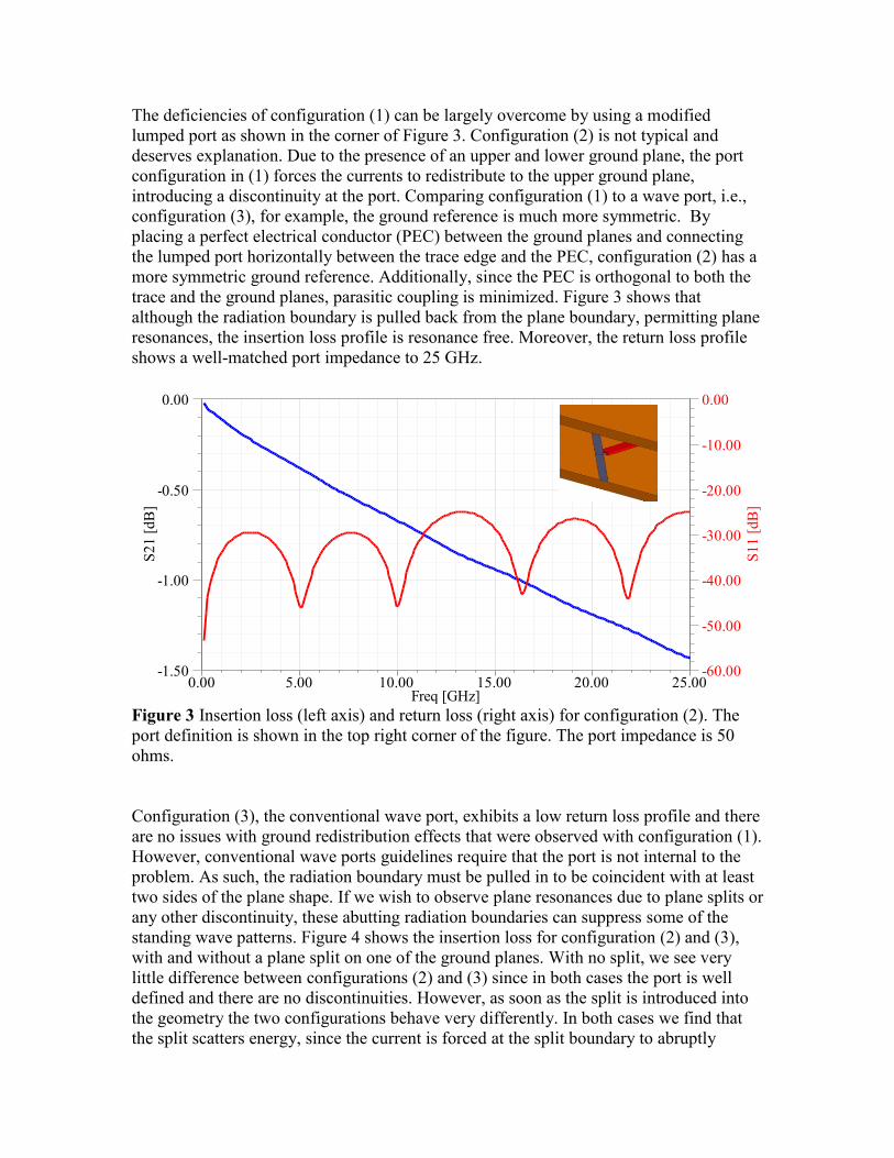
The deficiencies of configuration (1) can be largely overcome by using a modified
lumped port as shown in the corner of Figure 3. Configuration (2) is not typical and
deserves explanation. Due to the presence of an upper and lower ground plane, the port
configuration in (1) forces the currents to redistribute to the upper ground plane,
introducing a discontinuity at the port. Comparing configuration (1) to a wave port, i.e.,
configuration (3), for example, the ground reference is much more symmetric. By
placing a perfect electrical conductor (PEC) between the ground planes and connecting
the lumped port horizontally between the trace edge and the PEC, configuration (2) has a
more symmetric ground reference. Additionally, since the PEC is orthogonal to both the
trace and the ground planes, parasitic coupling is minimized. Figure 3 shows that
although the radiation boundary is pulled back from the plane boundary, permitting plane
resonances, the insertion loss profile is resonance free. Moreover, the return loss profile
shows a well-matched port impedance to 25 GHz.
Figure 3 Insertion loss (left axis) and return loss (right axis) for configuration (2). The
port definition is shown in the top right corner of the figure. The port impedance is 50
ohms.
Configuration (3), the conventional wave port, exhibits a low return loss profile and there
are no issues with ground redistribution effects that were observed with configuration (1).
However, conventional wave ports guidelines require that the port is not internal to the
problem. As such, the radiation boundary must be pulled in to be coincident with at least
two sides of the plane shape. If we wish to observe plane resonances due to plane splits or
any other discontinuity, these abutting radiation boundaries can suppress some of the
standing wave patterns. Figure 4 shows the insertion loss for configuration (2) and (3),
with and without a plane split on one of the ground planes. With no split, we see very
little difference between configurations (2) and (3) since in both cases the port is well
defined and there are no discontinuities. However, as soon as the split is introduced into
the geometry the two configurations behave very differently. In both cases we find that
the split scatters energy, since the current is forced at the split boundary to abruptly
0.00 5.00 10.00 15.00 20.00 25.00Freq [GHz]
-1.50
-1.00
-0.50
0.00
S2
1 [
dB
]
-60.00
-50.00
-40.00
-30.00
-20.00
-10.00
0.00
S1
1 [
dB
]
botslotw idth='0mil' offset='20mil' offsetFB='20

redistribute between the two ground planes. In the case of configuration (2) this energy
bounces about and excites the natural modal resonances of the cavity, very similar to the
response we see in Figure 2, although in that configuration the discontinuity was
introduced by the port itself. In the case of configuration (3), we find that although the
energy is scattered by the split, the radiation boundary prevents this energy from being
further reflected and consequently there are no resonances peaks in the insertion loss
profile. Instead, the entire profile has an increased slope due to the one-way energy loss
to the absorbing radiation boundary.
Figure 4 Insertion loss for configurations (2) and (3), with and without a plane split in
one of the ground planes. The port definition for configuration (3) is shown in the bottom
right corner of the figure. For simplicity, the radiation boundary was pulled in on all four
sides of the plane for configuration (3).
Configuration (4) could probably benefit from some explanation (see Figure 5). A
general requirement of a wave port is that one side of the port is on a non-solving side
(i.e. facing the background of the problem geometry or radiation boundary). This is
required in order to extend the wave port to a semi-infinitely long waveguide which is
used to excite the problem. By placing a PEC "cap" on one side of the wave port, we
have defined a surface which is non-solving, fulfilling this requirement. This
configuration enables us to pull the radiation boundary from the plane edge without
forcing us to rely on a lumped port.
0.00 5.00 10.00 15.00 20.00 25.00Freq [GHz]
-6.00
-5.00
-4.00
-3.00
-2.00
-1.00
0.00
S2
1 [
dB
]
(2) & (3) No split
(2) Split
(3) Split

Figure 5 Configuration 4 showing the PEC "cap", wave port face and offset radiation
boundary. This configuration permits standing wave patterns to be excited even on the
side of the plane where the wave port is defined.
Next we compare configurations (2) and (4). One of the benefits of configuration (2) is
small "footprint" of the port; as compared to the wave port dimensions, which can extend
over the entire width of the plane, configuration (2) is much smaller than the typical
wavelengths involved in the problems we are solving. Wave ports need to be a certain
minimum width in order to properly calculate the impedance of the port [3]. This
unintentional boundary condition created by the PEC cap and wave port can modify the
natural resonance patterns of the plane pair cavity. Figure 6 plots the insertion loss of the
single stripline trace using configuration (2) and (4). (Here we focus our attention on the
location of the first modal resonance but similar results and trends can be observed for
the higher frequency modal resonances). The port width used for configuration (4) was
varied from 10 mils to 100 mils (the full plane width) so the impact of the wave port size
could be examined. Making the port any narrower than 10 mils resulted in inaccuracies in
the calculation of the port impedance. The plot shows that as the port width is made
progressively narrower the modal resonance location approaches the simulated results for
configuration (2). This shows that smaller port widths and footprints help to minimize
the impact of the port on simulation results. However, if the port is made too narrow the
port impedance calculation may be inaccurate.
Offset
radiation
boundary
PEC cap
Wave port
face

Figure 6 Insertion loss for a stripline trace using configuration (2) and (4). The port
width used in configuration (4) was varied.
Additional questions arise when we consider coupled traces. Specifically, how do the port
configurations compare when strong coupling exists between two traces, as in a tightly
coupled differential pair. Taking it a step further, what if a plane split exists increasing
the coupling between the traces? Figure 7 shows that even when two traces are tightly
coupled and running over a 10 mil plane split, port configurations (2) and (3) show very
good agreement.
Figure 7 Near-end crosstalk between two traces using two different spacings and port
configurations. The 2.4 mil edge to edge spacing yields a 80 ohm differential impedance.
1.00 2.00 3.00 4.00 5.00 6.00 7.00 8.00 9.00 10.00Freq [GHz]
-7.00
-6.00
-5.00
-4.00
-3.00
-2.00
-1.00
0.00
S2
1 [
dB
]
(2)
Decreasing
wave port width
0.10 1.00 10.00 100.00Freq [GHz]
-70.00
-60.00
-50.00
-40.00
-30.00
-20.00
-10.00
S1
3 [
dB
]
1
(3)
(2)
2.4 mils
16.4 mils

In this section we have shown that
Port definition has a significant impact on the simulation results
Ports can act like a discontinuity scattering energy to the plane boundary
generating resonances if the planes aren’t properly terminated
Plane resonances can be suppressed using an abutting radiation boundary (or
proper termination) regardless of the port type
Even if the planes are properly terminated, incorrect port definition can increase
the overall loss of the structure
The drawbacks of the lumped port can be minimized using a modified lumped
port. We have shown, that the modified lumped port, not only injects energy into
the trace as good as the wave port, but also that works equally well for differential
pairs, and more importantly that it's very small, (considerably smaller than the
wave port).
2.2 Simulation Results
We have choices to make in our simulation setup before proceeding; by utilizing an
abutting radiation boundary, we can analyze split planes by looking at the impact on
signal propagation, in the absence of plane resonances. We can also examine the impact
of place resonances on signal propagation by offsetting the radiation boundary from the
plane edge. In order to fully understand the impact of the split on signaling we will
remove the effects of plane boundaries by abutting the radiation boundary against the
plane edge and use modified lumped ports to minimize the influence of the port. As we
have seen in the previous section, the scattering of energy due to the split can cause plane
resonances. However, these resonances are highly dependent on the particulars of the
split location in the board and overall power distribution network (PDN) design,
including the stackup, the amount of decoupling, etc. To simplify and generalize the
analysis these resonances will be ignored. This represents, for example, the case when
planes are perfectly terminated in the characteristic impedance of the plane pair. This is
also the case if the plane is electrically large and the signal and split are not near the plane
edge. One major exception to this is plane slots, as opposed to plane splits. In this case,
any energy coincident with the edge of the slot will not be completely absorbed − i.e., it
can be reflected and introduce resonances. By keeping the slot inside the absorbing
radiation boundary, we will be able to look at some of the unique characteristics of the
slot.
The test structure used for these simulations is shown in Figure 8. It consisted of either
two single-ended traces or two differential pairs routed (not shown) in a stripline
configuration. There are three plane layers and one signal layer in the stackup. Four vias,
located in each of the corners of the plane, provide connections between the upper and
lower ground planes. The middle plane represents a power plane and is not connected to
the vias. The top and bottom plane layers are always solid whereas the middle plane layer
can either be solid, slotted or split. A slot is defined as a split which doesn’t go the entire
width of the plane, i.e., it is an opening in the plane rather than a cut which extends across

the entire width. The solid plane layers above and below the slotted or split plane layer
represent the typical situation in a multilayer board where the slot or split does not exist
on all plane layers. Having a slot or split on all ground layers or even on the top most
layer, is not good design practice when signals are transversing the slot or split and
consequently this case is not specifically covered here. In the single-ended case we
concern ourselves with crosstalk, insertion and return loss. In the differential pair case we
concern ourselves with mixed mode crosstalk, mode conversion, mixed mode insertion
loss and return loss. The port numbering is also shown on Figure 8.
Figure 8 Two single-ended traces in a stripline configuration. A 20 mil split is shown in
the middle plane. Unless otherwise stated, the nominal dimensions are as follows: a plane
length of 500 mils, a plane width of 200 mils, the plane-to-plane separation is 10 mils, the
traces are 3.6 mil wide, centered vertically between the upper ground layer and power
layer, and routed 20 mils center to center.
Figure 9 plots the near-end crosstalk, insertion loss, return loss and far-end crosstalk for a
traces that have a 0.1%, 1% and 10% backward crosstalk coefficient (20, 12 and 6 mil
pitch, respectively) with the middle plane either split or solid. The crosstalk plot shows
that if the traces are lightly coupled then the split case will always introduce significantly
more crosstalk. However, as the traces get more tightly coupled the trace to trace
coupling can dominate the crosstalk. The insertion loss plot shows increased loss due to
the split for all cases. As the traces get more tightly coupled the even mode impedance
increases (to about 60 ohms in this case) resulting in the observed ripples in loss profile.
The return loss plot shows that the insertion loss ripple observed in the 10% coupling
case is due to the poor match. The far-end crosstalk plot is low overall for all cases due to
homogenous medium although the split itself does increase the crosstalk due to the
introduction of some inhomogeneity in the fields. Likewise, the tightly coupled trace,
even with the solid middle plane, increases the ultra-low baseline due to the asymmetry
compared to pure stripline.
Figure 10 plots the additional crosstalk, compared to the solid plane case, as a function of
trace pitch, extracted from Figure 9. Figure 10 shows that the baseline crosstalk is
increased in all cases, although the split is not as significant for the 10% coupling case.
A similar plot can be generated for the single-ended insertion loss however the jump in
single-ended insertion loss is fairly independent of trace pitch.
1
3
24

Figure 9 Moving clockwise from the top left plot the near-end crosstalk, insertion loss,
return loss and far-end crosstalk are shown as a function of trace pitch with the middle
plane either split or solid. Dashed arrow lines indicate the plane is split.
Figure 10 Additional crosstalk due to the split with different backward crosstalk
coefficients, extracted from Figure 9.
Figure 11 fixes the separation between the traces and sweeps the separation of the solid
ground plane at the bottom of the structure from the split ground plane (see Figure 8) in
the following steps: 2.5, 5, 7.5, 10 and 30 mils. The solid middle plane data is also shown
for reference. This plot shows that the separation between the lower ground plane and
split can significantly impact both the crosstalk induced by the split and the insertion loss.
Although the crosstalk is still significantly higher than a solid middle plane in absolute
terms (> -80 dB), in practical terms the crosstalk induced by the split can be eliminated
by using a closely placed solid lower ground.
0.10 1.00 10.00 100.00Freq [GHz]
-80.00
-70.00
-60.00
-50.00
-40.00
-30.00
-20.00
-10.00
0.00
S3
1 [
dB
]
Impact of Trace Spacing on NEXT w/ and w/o the Split
0.00 5.00 10.00 15.00 20.00Freq [GHz]
-1.60
-1.40
-1.20
-1.00
-0.80
-0.60
-0.40
-0.20
0.00
S2
1 [
dB
]
Impact of Trace Spacing on Insertion Loss w/ and w/o the Split2
0.10 1.00 10.00 100.00Freq [GHz]
-100.00
-90.00
-80.00
-70.00
-60.00
-50.00
-40.00
-30.00
-20.00
-10.00
0.00
S4
1 [
dB
]
Impact of Trace Spacing on FEXT w/ and w/o the Split1
0.00 5.00 10.00 15.00 20.00Freq [GHz]
-70.00
-60.00
-50.00
-40.00
-30.00
-20.00
-10.00
0.00
S1
1 [
dB
]
Impact of Trace Spacing on Return Loss w/ and w/o the Split1
10%
1%
split0.1%
split
0.1%, 1%
solid
10%
solid
0.1%, 1%
split
0.1%, 1%
solid
10%
split
1%
solid
0.1%
solid
10%
split
10%
solid
-40
-20
0
20
40
60
80
0.1 1 10
Incr
ease
in N
EX
T [%
]
Frequency [GHz]
10%
0.1% 1%

Figure 11 Moving clockwise from the top left plot the near-end crosstalk, insertion loss,
return loss and far-end crosstalk are shown as a function of split to bottom ground
distance. The trace to trace pitch is fixed at 20 mil (0.1%). Dashed arrow lines indicate
the plane is split.
Figure 12 extracts the near end crosstalk and insertion loss values from Figure 11 at 4
GHz and compares them to the full-plane case (no split). Several additional lower ground
separation points were also simulated to show how the increase in crosstalk and insertion
loss flattens out as the plane is further distanced from the split. The figure shows that as
the lower ground plane gets closer to the split, the crosstalk and insertion loss levels
approach that of a solid plane. The separation distance where the ground plane
significantly loses its effectiveness is 1-2 X the slot width. Other split widths were also
simulated (e.g. 10 mil) while sweeping the lower ground plane separation and the trends
and absolute values plotted in Figure 12 remained nearly the same.
Figure 12 Increase in crosstalk (left) and in insertion loss (right) as a function of the
lower ground plane separation to split width ratio. The crosstalk and insertion loss values
were extracted from Figure 11 at 4 GHz and normalized to the crosstalk and insertion
loss value for the case where there is a full plane (no split).
0.10 1.00 10.00 100.00Freq [GHz]
-80.00
-70.00
-60.00
-50.00
-40.00
-30.00
-20.00
-10.00
0.00
S3
1 [
dB
]
Impact of GND Spacing on NEXT w/ and w/o the Split
0.00 5.00 10.00 15.00 20.00Freq [GHz]
-1.80
-1.60
-1.40
-1.20
-1.00
-0.80
-0.60
-0.40
-0.20
0.00
S2
1 [
dB
]
Impact of GND Spacing on Insertion Loss w/ and w/o the Split
0.10 1.00 10.00 100.00Freq [GHz]
-100.00
-90.00
-80.00
-70.00
-60.00
-50.00
-40.00
-30.00
-20.00
-10.00
0.00
S4
1 [
dB
]
Impact of GND Spacing on FEXT w/ and w/o the Split
0.00 5.00 10.00 15.00 20.00Freq [GHz]
-60.00
-50.00
-40.00
-30.00
-20.00
-10.00
0.00
S1
1 [
dB
]
Impact of GND Spacing on Return Loss w/ and w/o the Split
2.5mils
30mils
solid
2.5mils30mils
solid
solid
solid
2.5mils
30mils
100
110
120
130
140
150
0 1 2 3 4 5 6
Incr
ease
in C
ross
talk
[%
]
Lower ground separation to split width ratio [-]
solid plane
100
110
120
130
140
150
160
170
180
0 1 2 3 4 5 6
Incr
ease
in I
nse
rtio
n L
oss
[%
]
Lower ground separation to split width ratio [-]
solid plane

Figure 13 examines the impact of the width of the split on the single-ended parameters.
The width of the split was varied as follows: 5, 10, 20, 40, 60 mil. All the s-parameters
are impacted by the width of the split although the largest impact is on return loss. As
expected, the insertion loss and crosstalk increase as the split width grows. However,
based on the narrow range in which the crosstalk and insertion loss is affected by the split
width, it would be fair to say that the width of the split is not nearly as important as the
presence of the split.
Figure 13 Moving clockwise from the top left plot the near-end crosstalk, insertion loss,
far-end crosstalk and return loss are shown as a function of width. The trace to trace pitch
is fixed at 20 mil (0.1%). Dashed arrow lines indicate the plane is split.
Next, we examine the impact of the slot (versus split) on the single ended parameters.
The slot is different than the split in that energy which exists due to the discontinuity of
the plane can be reflected by the metal sides of the slot, allowing for additional loss and
resonances. The lowest possible resonance that can exist between the edges of the slot is
the half-wave resonance. In the case of the split, there is also the possibility of
resonances due to the impedance discontinuity, since the split's characteristic impedance
is different than its boundaries (both along the split's width and length). However, the
absorbing boundary conditions effectively terminates the split discontinuity along its
length, suppressing any resonances.
0.10 1.00 10.00 100.00Freq [GHz]
-80.00
-70.00
-60.00
-50.00
-40.00
-30.00
-20.00
-10.00
0.00
S3
1 [
dB
]
Impact of Split Width on NEXT
0.00 5.00 10.00 15.00 20.00Freq [GHz]
-60.00
-50.00
-40.00
-30.00
-20.00
-10.00
0.00
S1
1 [
dB
]
Impact of Split Width on Return Loss
0.00 5.00 10.00 15.00 20.00Freq [GHz]
-1.80
-1.60
-1.40
-1.20
-1.00
-0.80
-0.60
-0.40
-0.20
0.00
S2
1 [
dB
]
Impact of Split Width on Insertion Loss
0.10 1.00 10.00 100.00Freq [GHz]
-100.00
-90.00
-80.00
-70.00
-60.00
-50.00
-40.00
-30.00
-20.00
-10.00
0.00
S4
1 [
dB
]
Impact of Split Width on FEXT
5mils
30mils
solid 5mils
5mils
30mils
solid
30mils
solid
5mils
30mils
solid

Figure 14 shows the complex electric field at 13 GHz (left) and 25 GHz (right) on the
same structure as shown in Figure 8 except the plane width was 400 mil as opposed to
200 mil, in order to allow for a lower half wave resonance frequency. The slot is 200 mil
wide which corresponds to a half-wave resonance of approximately 13 GHz. In these
plots the trace on the right is the aggressor and the trace on the left is the victim. Figure
16 plots the single-ended s-parameters for different slot widths. We find that the crosstalk
peaks line up with where the slot is approximately the half-wave resonance frequency.
Furthermore, in all cases, the peak crosstalk is higher than the split plane case.
Figure 15 Complex electric field at 13 GHz (left) and 25 GHz (right) on the 400 mil
wide power plane with a 200 mil cutout. The definition of slot length and slot width are
defined on the left graph.
To systematically investigate the impact of the slot resonance on the insertion loss and
near end crosstalk, a number of simulation sweeps were performed. Figure 17 plots the
near-end crosstalk (left) and insertion loss (right) as a function of slot length. The slot
length was swept over the following values: 398, 394, 390, 386, 384, 380, 350, 340, 300,
260, 220, 200, 180, 140, 100, 60, 50, 40, 30, 20, 10, 4 mils. Also shown are the slot
length extremes, namely: slot length is zero (solid plane) and slot length is 400 mils (split
plane). Figure 17 shows that the low frequency conversion of crosstalk is quite sensitive
to slot length. Only when the slot is approximately 10 mils does the crosstalk picture start
to resemble the solid plane case. The data shown on Figure 17 can be further post-
processed and the difference between the slotted case and the split or solid plane case can
be plotted. These plots are shown in Figure 18 and Figure 19, respectively. In Figure 18,
we see the slot can increase crosstalk and have greater loss than the split plane case.
Note that these trends are not as visible in the crosstalk plot of Figure 19 because the
width
length

solid plane case is dominated by the peaks and valleys associated with trace to trace
crosstalk over a solid plane.
Figure 20 shows two curves; the blue curve is the extracted frequency where the NEXT
peaks in Figure 17 (left). The red curve shows the half wave resonance based on the slot
length. At low frequencies, the half wavelength of the slot is so low in frequency that we
don't see the effect of the slot. In this region, we see the effect of the split more than the
slot on crosstalk; with the split, the crosstalk peaks and valleys tend to be smoothed out
and, in general, the higher the frequency, the higher the crosstalk. As the slot gets shorter,
we start to see the peak in the NEXT lining up with the half wavelength of the slot.
Above about 140 mils, the half wavelength is higher in frequency than what we
simulated, so the NEXT maximum is always 25 GHz. Finally, for the shortest slot
lengths, we return to the solid-plane-like case, where we observe the peaks and valleys of
the crosstalk and the maximum NEXT occurs at the quarter-wave peak.
Figure 16 Moving clockwise from the top left plot the near-end crosstalk, insertion loss,
return loss and far-end crosstalk are shown for various slot lengths. The slot width is
fixed at 20 mils. The trace to trace pitch is fixed at 20 mil (0.1%). Dashed arrow lines
indicate the plane is slotted.
0.00 5.00 10.00 15.00 20.00 25.00Freq [GHz]
-50.00
-45.00
-40.00
-35.00
-30.00
-25.00
S3
1 [
dB
]
Impact of Slot on NEXT
0.00 5.00 10.00 15.00 20.00 25.00Freq [GHz]
-2.00
-1.50
-1.00
-0.50
0.00
S2
1 [
dB
]
Impact of Slot on Insertion Loss
0.00 5.00 10.00 15.00 20.00 25.00Freq [GHz]
-50.00
-45.00
-40.00
-35.00
-30.00
-25.00
S4
1 [
dB
]
Impact of Slot on FEXT
0.00 5.00 10.00 15.00 20.00 25.00Freq [GHz]
-55.00
-50.00
-45.00
-40.00
-35.00
-30.00
-25.00
-20.00
-15.00
S1
1 [
dB
]
Impact of Slot on Return Loss
200mil
300mil
350mil
solid
200mil
300mil
350mil
solid
200mil
300mil
350mil
solid

Figure 17 Impact of slot length on near-end crosstalk (left) and insertion loss (right).
Figure 18 Impact of slot length on near end crosstalk (left) and insertion loss (right). The
quantity plotted is the difference between the slotted case and the split plane case.
Figure 19 Impact of slot length on near end crosstalk (left) and insertion loss (right). The
quantity plotted is the difference between the slotted case and the solid plane case. The
split plane case is also plotted at the far end, i.e. slot length is the full plane width.
Additional simulations were run examining the impact of trace length and slot width on
the additional crosstalk and insertion loss. Simulations showed that wider slots will
modify the exact slot resonance location although the trends and magnitudes remained
the same.
400384
260100
20
-100
-80
-60
-40
-20
14
71013
16192225
Slot Length [mil]
Nea
r E
nd
Cro
ssta
lk [d
B]
Frequency [GHz]
solid
split
400
380
20020
-2
-1.5
-1
-0.5
0
1 4 7 10 13 16 19 22 25Slot Length
[mil]
Inse
rtio
n L
oss
[d
B]
Frequency [GHz]
split
solid
398
340
1000
0.05
0.1
0.15
0.2
1 4 7 10 13 16 192225Slot
length [mil]
Ad
dit
ion
al In
sert
ion
Lo
ss [d
B]
Frequency [GHz]
398
340
1000
1
2
3
4
1 4 7 10 13 16 192225Slot
length [mil]
Ad
dit
ion
al N
EX
T [d
B]
Frequency [GHz]
40
0
38
4
26
0
10
0
20
0102030
40
50
15
913
1721
25
Slot Length [mil]
Ad
dit
ion
al C
ross
talk
[d
B]
Frequency [GHz]
split
40
0
38
4
26
0
10
0
20
0
0.2
0.4
0.6
0.8
15
913
1721
25
Slot Length [mil]
Ad
dti
onal
In
sert
ion L
oss
[d
B]
Frequency [GHz]
split

Figure 20 Frequency for peak crosstalk as a function of slot length (blue). Also shown is
the half wave resonance of the slot (red). These data are for a 400 x 500 mil plane with a
20 mil slot.
Finally, we turn our attention to two neighboring differential pairs passing over a split or
slotted plane. In this case we concern ourselves with the mixed-mode s-parameters.
Figure 21 plots the mixed mode s-parameters for a differential pair where the intra
differential pitch is 12 mil (1%) and the inter-differential pitch is 20 mil (0.1%). This
represents a typical case where the differential pair is loosely coupled and neighboring
pairs are spaced to reduce pair to pair coupling. The plots show that the presence of the
split increases the pair to pair differential crosstalk compared to the solid plane case. Also
shown on the plots are the s-parameter for an inter differential pitch of 30 mil (0.01%).
This additional spacing (30 mil versus 20 mil) is required to achieve the same level of
crosstalk as the solid plane case. However, notice the difference in crosstalk levels above
3 GHz; the peaks observed in the near-end crosstalk for the solid plane case1, which serve
to reduce the overall crosstalk, are saturated in the case of the split plane. This makes it
challenging to sufficiently separate traces to achieve the same overall crosstalk,
especially at high frequencies. Notice that the split increases the differential to common-
mode conversion as well. Again, increasing the inter pair pitch to 30 mil is required to
achieve the same mode conversion as the as the solid plane case.
1 The first maxima of the S31 profile occurs at λ/4 of the coupled line length. The subsequent peaks occur
at the odd harmonics of λ/4.
0
5
10
15
20
25
39
8
39
0
38
4
35
0
30
0
22
0
18
0
10
0
50
30
10 0
Fre
qu
ency
[G
Hz]
Slot length [mil]
peak
crosstalk
lambda/2

Figure 21 Moving clockwise from the top left plot the differential near-end crosstalk,
differential insertion loss, differential return loss and differential to common-mode
conversion are shown for two differential pairs over a split and solid plane. The dashed-
traces are for the split plane.
Figure 22 plots the additional mixed mode near end crosstalk due to a split (relative to a
solid plane) for the following inter and intra pitches: 6 and 12 mils, 12 and 20 mils, 8 and
15 mils. These correspond to the following backward crosstalk coefficients, respectively:
10 and 1%, 5 and 0.5%, 1 and 0.1%. These values were chosen such that the pair to pair
coupling was kept constant, yielding about 1/10th of the intra coupling. This plot shows a
number of interesting features: first, the more strongly coupled differential pairs are, the
less the impact of the split on crosstalk. Second, we observe that the greatest increase in
crosstalk occurs above the λ/4 of the coupled line length. In this frequency region, even
tightly coupled differential pairs can exhibit significantly more pair to pair coupling.
Similar peaks were obtained from the single-ended crosstalk simulations, shown in
Figure 10.
108
109
1010
1011
-100
-80
-60
-40
-20
Frequency [Hz]
DIF
F N
ear
End C
rossta
lk [
dB
]
0 0.5 1 1.5 2
x 1010
-70
-60
-50
-40
-30
-20
Frequency [Hz]
DIF
F R
etu
rn L
oss [
dB
]
0 0.5 1 1.5 2
x 1010
-120
-100
-80
-60
-40
Frequency [Hz]
DIF
F-C
M C
onvers
ion [
dB
]
0 0.5 1 1.5 2
x 1010
-1.5
-1
-0.5
0
Frequency [Hz]
DIF
F I
nsert
ion L
oss [
dB
]
Split
0.01%
Split
0.1%
Solid
0.1%
Split
0.01%
Split
0.1%
Solid
0.1%
Split
0.01%
Split
0.1%
Solid
0.1%

Figure 22 Additional differential near end crosstalk due to split.
In this section we have found
Solid ground planes immediately below splits can minimize the effect of the split
on signal propagation if separated less by than 1-2X the split width vertically.
Split width is not nearly as important a parameter as the presence of a split.
Crosstalk between single ended traces is significantly higher in the presence of a
split plane.
Slots can introduce greater peak crosstalk than splits due to resonances setup by
the slot edges.
Splits increase the crosstalk between differential pairs and increase the differential
to common-mode noise conversion.
The greatest increase in crosstalk due to a split (relative to a solid plane) occurs
above the λ/4 of the coupled line length. When one considers this frequency
region, it is practically difficult to separate differential pairs in the presence of a
split such that the crosstalk is the same as if the plane was solid.
2.3 Test Board Specifications, Measurement
Procedure and Correlation Results
A scaled test structure was constructed to correlate the simulation environment. The
board consisted of two 3 mm wide striplines routed on a pitch of 10 mm center to center.
The plane dimensions are 2440 mil wide and 6496 mil long. The two traces are vertically
centered in a 126 mil thick FR4 dielectric. Figure 23 (left) shows a snapshot of the test
structure. The purpose of making a test structure using these large dimensions relative to
typical printed circuit board dimensions was to facilitate milling the bottom copper plane
and introducing various slots and splits.
As shown on the left photo in Figure 23, the scaled test board had two edge-launch SMA
connectors. At each step of milling, the impedance profile and the S-parameters were
measured with two separate instruments. Once the solid plane case was measured, a 125
0 0.5 1 1.5 2
x 1010
-50
-40
-30
-20
-100
10
20
30
4050
Frequency [Hz]
Ad
ditio
na
l C
rossta
lk [
%]
10%,1%
1%, 0.1%
5%, 0.5%

mil wide slot was milled that was 2000 mil long followed by a full split (also 125 mil
wide). The slot and split were located at the midpoint along the total length of the
structure. The right-hand chart of Figure 23 shows the impedance profile of the structure
with the slot and split. Since the trace dimensions were scaled, these dimensions yielded a
measured differential impedance of 65 ohms (2D simulations predicted 68 ohms). The
presence of the slot and split is clearly visible in the center of the profile, resulting in a
sharp increase in the trace impedance. The solid plane’s TDR profile was flat, indicating
65 ohms. At each milling step, the S-parameters of the structures were also measured in
the frequency range from 10 MHz to 20 GHz with an Agilent E8363A VNA unit.
Figure 23 Photo of the scaled test structure after milling the split (left). Impedance
profile of the trace over a slot and split plane (right).
Ansoft HFSS was used to solve for the S-parameters of the test structure. In order to
evaluate the accuracy of our simulation environment, the same parameterizable project
which was used for Section 2 was used, only the dimensions where scaled. This ensures
that the project environment, port definition and analysis setup are the same. Because of
the large physical size of the test structure compared to the wavelengths involved, the
structure was only analyzed up to 10 GHz.
Figure 24 shows the measurement and simulation data plotted for the split plane case.
Good correlation is observed between measurement and simulation. Similarly good
correlation was obtained for the slot and solid plane case.
50
55
60
65
70
75
80
190 250 310 370 430 490 550 610
Imp
edan
ce [o
hm
s]
[-]
split
slot
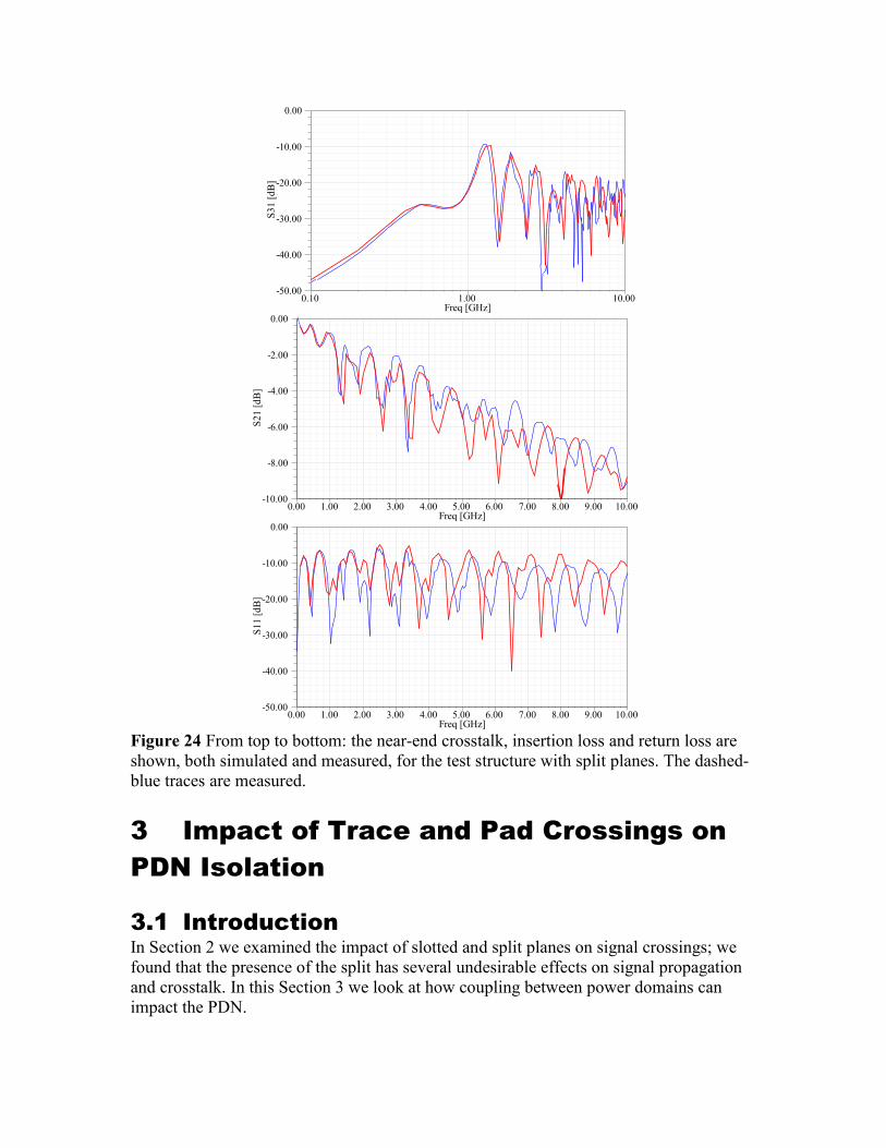
Figure 24 From top to bottom: the near-end crosstalk, insertion loss and return loss are
shown, both simulated and measured, for the test structure with split planes. The dashed-
blue traces are measured.
3 Impact of Trace and Pad Crossings on
PDN Isolation
3.1 Introduction
In Section 2 we examined the impact of slotted and split planes on signal crossings; we
found that the presence of the split has several undesirable effects on signal propagation
and crosstalk. In this Section 3 we look at how coupling between power domains can
impact the PDN.
0.10 1.00 10.00Freq [GHz]
-50.00
-40.00
-30.00
-20.00
-10.00
0.00
S3
1 [
dB
]
Near End Crosstalk - SPLIT
0.00 1.00 2.00 3.00 4.00 5.00 6.00 7.00 8.00 9.00 10.00Freq [GHz]
-50.00
-40.00
-30.00
-20.00
-10.00
0.00
S1
1 [
dB
]
Return Loss - SPLIT
0.00 1.00 2.00 3.00 4.00 5.00 6.00 7.00 8.00 9.00 10.00Freq [GHz]
-10.00
-8.00
-6.00
-4.00
-2.00
0.00
S2
1 [
dB
]
Insertion Loss - SPLIT

Coupling between otherwise independent power domains can occur due to a variety of
reasons: a) edge coupling of adjacent plane shapes sharing the same layer, b) broadside
coupling of plane shapes in adjacent vertical layers, c) traces or component pads running
over adjacent plane shapes, d) stitching capacitors intentionally placed between adjacent
power shapes. With the exception of d), which has limited efficiency at higher
frequencies, all other coupling mechanisms are distributed in nature, but at low
frequencies the transfer impedance can be simply approximated by a capacitive PI circuit
of self capacitances and coupling capacitance. Vertically aligned or partially aligned
power plane shapes create the strongest coupling because of their broadside nature, and in
this case the only way to reduce the coupling is to either reduce the overlapping area, or
to increase the self capacitance of each power domain by either increasing the
corresponding dielectric constant or by reducing the distance to their nearest ground
plane. At high frequencies the coupling becomes distributed and at least a 2D model is
necessary to capture the proper behavior [4].
Although the impact of traces and pad split crossings on the self-impedance is usually
small, it can be discernable: sometimes it shows up as a split in the resonance impedance
peak. On the other hand, the impact of these crossings on the transfer impedance or
isolation between planes can be much greater. Power domains are isolated for several
reasons. For example, noise sensitive circuits (such as phase-locked loops) may need to
be isolated from noisy high speed digital circuits. The risk with these trace and pad split
crossings is an increase in coupling such that noise isolation is compromised between
power domains.
3.2 DUT Specifications, Measurement Procedure
and Correlation Results
A multilayer board shown in Figure 25 was used to correlate the Ansoft SIwave
simulation environment used for the PDN simulations. A single layer from a multilayer
board is shown; the layer consists of an outer rail (C shaped, highlighted in yellow), an
inner rail (rectangular, with cutout, highlighted in blue) , and a trace and pad transversing
the split (identified with arrows).
Figure 26 (left) plots the simulated and measured isolation between these two plane
shapes. The self impedance of each domain is relatively low and therefore simply the S21
parameters are used as a measure of isolation. Figure 26 (left) shows several interesting
features including a broad low-frequency hump and a couple of high-frequency peaks;
the simulation does a good job of capturing the magnitude and location of the hump and
higher-order peaks. Figure 26 (right) plots the measured isolation when the trace was
manually cut at the split and the pad, bridging over the two power shapes, was peeled
away. The plot shows how these relatively small inadvertent plane crossings can
significantly alter isolation between the rails; not only is the low frequency hump
increased but the peak amplitude of the resonance at 450 MHz is significantly increased.
Note that in order to achieve the level of correlation shown in Figure 26, it was very
important to properly capture all aspects of the plane to plane coupling including:
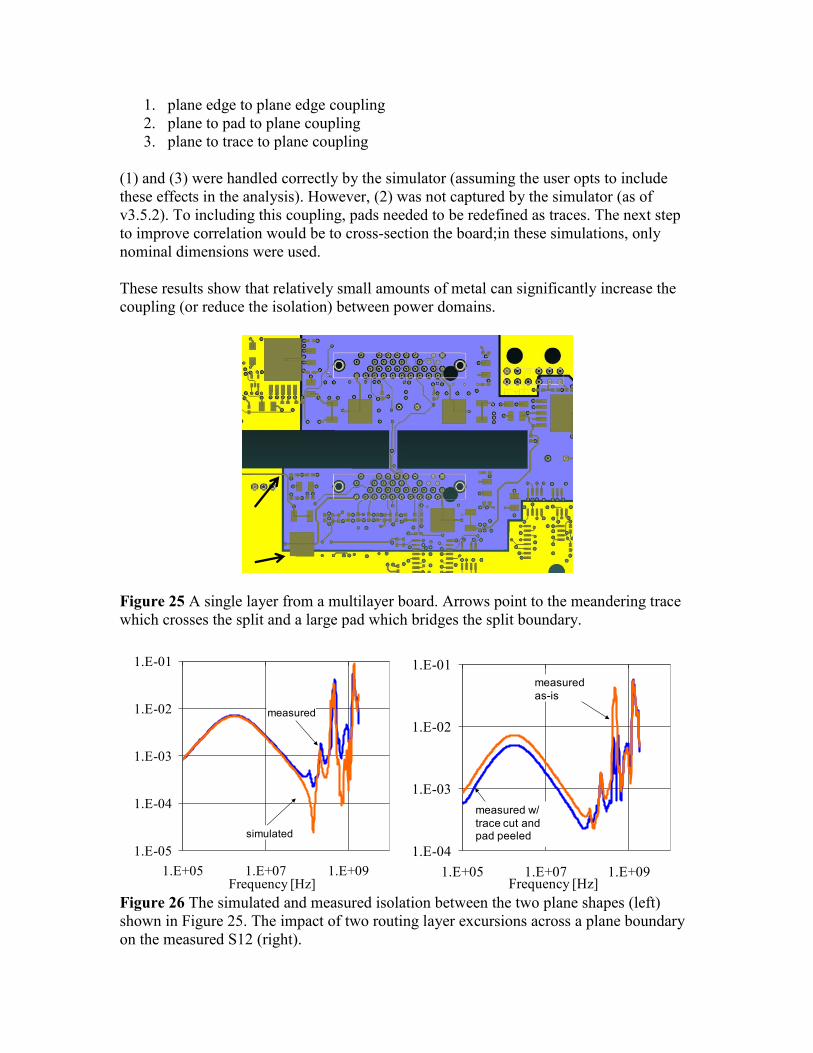
1. plane edge to plane edge coupling
2. plane to pad to plane coupling
3. plane to trace to plane coupling
(1) and (3) were handled correctly by the simulator (assuming the user opts to include
these effects in the analysis). However, (2) was not captured by the simulator (as of
v3.5.2). To including this coupling, pads needed to be redefined as traces. The next step
to improve correlation would be to cross-section the board;in these simulations, only
nominal dimensions were used.
These results show that relatively small amounts of metal can significantly increase the
coupling (or reduce the isolation) between power domains.
Figure 25 A single layer from a multilayer board. Arrows point to the meandering trace
which crosses the split and a large pad which bridges the split boundary.
Figure 26 The simulated and measured isolation between the two plane shapes (left)
shown in Figure 25. The impact of two routing layer excursions across a plane boundary
on the measured S12 (right).
1.E-04
1.E-03
1.E-02
1.E-01
1.E+05 1.E+07 1.E+09Frequency [Hz]
measured
as-is
measured w/
trace cut and pad peeled
1.E-05
1.E-04
1.E-03
1.E-02
1.E-01
1.E+05 1.E+07 1.E+09Frequency [Hz]
measured
simulated

4 Conclusions
Signals transversing splits or slots can have energy reflected due to the discontinuity.
Energy will also be introduced into the split or slot itself which can introduce a host of
additional issues, some of which were explored in this paper. We showed that this energy
not only increases crosstalk to neighboring traces but it can also excite the slot,
generating additional resonances, causing more crosstalk and additional loss beyond the
split case. We found that differential signals do not side step the problem of slots and
split entirely although strong coupling can help to reduce their impact. Although not
specifically explored here slots and splits may also cause radiation and EMI problems.
We explored ways to mitigate the impact of the split by placing a solid ground plane
immediately below the split and found that a solid ground plane below the split is
effective if separated less by than 1-2X the split width vertically. We also found that the
split width is not nearly as important as the presence of the split itself.
In all of these simulations we purposely ignored any plane resonances generated by the
split. This mimics the case when planes are either perfectly terminated, well bypassed or
the case when the plane is electrically large and the signal and split are not near the plane
edge. However, if these conditions aren't consistently maintained in production boards,
these resonances can have a significant, and in many cases, dominant, impact on the
signal propagation, as we saw from some of the port definition figures. We also looked at
the impact of traces and pads on the isolation between power domains and found that
relatively small amounts of metal can significantly increase the coupling between the
domains.
Throughout the paper an emphasis has been placed on “calibrating” our simulation
environment to get accurate results. We found that ports need to be defined very carefully
to ensure that the discontinuity of the port itself doesn’t influence the results. Lastly, it
was shown that accurately simulating plane-to-plane coupling (in order to achieve good
measurement to simulation correlation), requires carefully including all of the different
coupling mechanisms.
Acknowledgements
Thanks to Jim Delap of Ansoft Corporation for his help with port definitions.
References
1. Jason R. Miller, Istvan Novak. Frequency Domain Characterization of Power Distribution Networks. Artech House, 2007, pp. 35-36. 2. Gustavo Blando, Jason R. Miller, Douglas Winterberg, and Istvan Novak, "Crosstalk in Via Pin-Fields Including the Impact of Power Distribution Structures," Proceedings of DesignCon 2009, February 2009. 3. Jason R. Miller, Istvan Novak. Frequency Domain Characterization of Power Distribution Networks. Artech House, 2007, pp. 34-35. 4. Madhavan Swaminathan, Ege Engin, Power Integrity Modeling and Design for Semiconductors and Systems, Prentice Hall, 2008.