Embed Size (px)
Citation preview

© Semiconductor Components Industries, LLC, 2012
June, 2012 − Rev. 11 Publication Order Number:
EVBUM2126/D
NCP1030GEVB
Isolated 2 W Bias Supply forTelecom Systems Using theNCP1030 Evaluation BoardUser's Manual
IntroductionPower converters using secondary side controllers
provide better transient response, higher efficiency andusually require less components than their primary sidereferenced counterparts. However, secondary sidecontrollers require a primary side referenced bias supply tostart operation. After start−up, the controller power can beprovided from the secondary side.
The NCP1030 incorporates in a single IC all the activepower, control logic and protection circuitry required forimplementing, with a minimum of external components, ahighly integrated isolated bias supply. The features includedin the NCP1030 can result in a footprint area reduction by upto 91% compared to a solution implemented using discretecomponents.
The NCP1030 Power Switch Circuit is rated at 200 V,making it ideal for 48 V Telecom and 42 V automotiveapplications. In addition, this IC can operate from anexisting 12 V supply. The NCP1030 includes an extensiveset of features including:• On Board Power Switch: Eliminates the need for an
external switch. As the Power Switch characteristicsare well known the gate drive is tailored to controlswitching transitions and help reduce electromagneticinterference (EMI).
• An Internal Start−up Regulator: Provides power tothe NCP1030 during start−up. After start−up, theregulator is disabled, thus reducing power consumption.The regulator can be powered directly from the inputline.
• Internal Error Amplifier: Allows the implementationof an isolated supply using primary side regulationwithout the need for an optocoupler.
• Internal Cycle by Cycle Current Limit: Eliminatesthe need for external sensing components. Theprogrammed current limit is 500 mA.
• Proprietary Active Leading Edge Blanking (LEB)Circuit: Provides better current limit control comparedto a fixed blanking period. The active LEB circuitmasks the current signal during the Power Switch turnON transition.
• Individual Line Undervoltage and Overvoltage(UV/OV) Detectors with Hysteresis: Eliminate theneed for external supervisory function. The UV/OVdetectors can be disabled if not needed.
• Single Capacitor Oscillator: Eliminates traditionaltiming resistor. Oscillator is optimized for operation upto 1.0 MHz.
• Internal �2% Voltage Reference: Eliminates theneed for an external bypass capacitor.
• Thermal Shutdown Circuit: Protects the device in theevent the maximum junction temperature is exceeded.
Design SpecificationsAn isolated bias supply for a telecom system is designed
and implemented using the NCP1030. The supply delivers2.0 W at 12 V. The converter specifications are listed inTable 1.
Table 1. BIAS SUPPLY SPECIFICATIONS
Parameter Symbol Min Max
Input Voltage Vin 35 V 76 V
Frequency � 250 kHz 300 kHz
Peak Efficiency � 80% −
Output Voltage Vout 10.8 V 13.2 V
Output Current Iout 0.017 A 0.17 A
Output Power Pout 2.0 W −
A Flyback topology operating in discontinuous mode isselected because of its simplicity and low part count.
http://onsemi.com
EVAL BOARD USER’S MANUAL
NCP1030GEVB
http://onsemi.com2
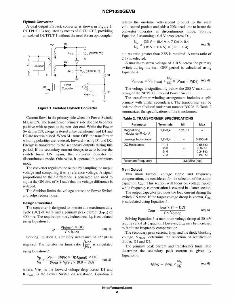
Flyback ConverterA dual output Flyback converter is shown in Figure 1.
OUTPUT 1 is regulated by means of OUTPUT 2, providingan isolated OUTPUT 1 without the need for an optocoupler.
Figure 1. Isolated Flyback Converter
TX
D2
+
−
R2
+
−
EAPWM
Controller
+
−
+
−
D1
+
−
R1
M1
SnubberVin
Cout Vout (OUTPUT1)
CCC VCC (OUTPUT2)
VREF
Current flows in the primary side when the Power Switch,M1, is ON. The transformer primary side dot end becomespositive with respect to the non−dot end. While the PowerSwitch is ON, energy is stored in the transformer and D1 andD2 are reverse biased. When M1 turns OFF, the transformerwinding polarities are reversed, forward biasing D1 and D2.Energy is transferred to the secondary outputs during thisperiod. If the secondary current decays to zero before theswitch turns ON again, the converter operates indiscontinuous mode. Otherwise, it operates in continuousmode.
The converter regulates the output by sampling the outputvoltage and comparing it to a reference voltage. A signalproportional to their difference is generated and used toadjust the ON time of M1 such that the voltage difference isreduced.
The Snubber limits the voltage across the Power Switchand helps reduce noise.
Design ProcedureThe converter is designed to operate at a maximum duty
cycle (DC) of 40 % and a primary peak current (IPPK) of400 mA. The required primary inductance, LP, is calculatedusing Equation 1.
Lp �Vin(min) � DC
f� IPPK(eq. 1)
Solving Equation 1, a primary inductance of 127��H is
required. The transformer turns ratio �NpNs� is calculated
using Equation 2
NpNs
�(Vin � (IPPK � RDS(on))) � DC
(Vout � VfD1) � (0.8 � DC)(eq. 2)
where, VƒD1 is the forward voltage drop across D1 andRDS(on) is the Power Switch on resistance. Equation 2
relates the on−time volt−second product to the resetvolt−second product and adds a 20% dead time to insure theconverter operates in discontinuous mode. SolvingEquation 2 assuming a 0.5 V drop across D1,
NpNs
�(35 V � (0.4 A � 7 �)) � 0.4
(12 V � 0.5 V) � (0.8 � 0.4)(eq. 3)
a turns ratio greater than 2.58 is required. A turns ratio of2.78 is selected.
A maximum stress voltage of 110 V across the primaryswitch during the turn OFF period is calculated usingEquation 4.
Vstress � Vin(max) �NpNs
� (Vout � VfD1) (eq. 4)
The voltage is significantly below the 200 V maximumrating of the NCP1030 internal Power Switch.
The transformer winding arrangement includes a splitprimary with bifilar secondaries. The transformer can beordered from Coilcraft under part number B0226−E. Table 2summarizes the specifications of the transformer.
Table 2. TRANSFORMER SPECIFICATIONS
Parameter Terminals Min Max
MagnetizingInductance @ 0.4 A
1,2−3,4 102 �H −
Leakage Inductance 1,2−3,4 − 0.955 �H
DC Resistance 1−42−35−67−8
−−−−
0.655 �0.82 �0.248 �0.248 �
Resonant Frequency − 3.8 MHz (typ.)
Main OutputTwo main factors, voltage ripple and frequency
compensation, are considered for the selection of the outputcapacitor, Cout. This section will focus on voltage ripple,while frequency compensation is covered in a latter section.
The output capacitor provides the load current during theswitch ON time. If the target voltage droop is known, Coutis calculated using Equation 5.
Cout �Iout � (1 � DC)
f� Vdroop(eq. 5)
Solving Equation 5, a maximum voltage droop of 50 mVrequires a 7.4 �F capacitor. However, Cout may be increasedto facilitate frequency compensation.
The secondary peak current, ISPK, and the diode blockingvoltage, Vblock, determine the selection of rectificationdiodes, D1 and D2.
The primary peak current and transformer turns ratiodetermine the secondary peak current as given byEquation 6.
ISPK � IPPK �NpNs
(eq. 6)
NCP1030GEVB
http://onsemi.com3
The voltage across the rectification diode is given byEquation 7.
Vblock � Vout � Vin(max) ��NsNp� (eq. 7)
Solving Equations 6 and 7, the rectification diode needsto handle 1.11 A and 39.34 V. In addition to the voltagecalculated using equation 7, voltage spikes during switchingtransitions need to be considered when selecting theblocking voltage rating. A Schottky diode is selected toreduce the forward voltage drop, thus reducing powerdissipation. On Semiconductor’s MBRA160 is selected as itmeets all the requirements.
Auxiliary Supply RegulatorThe auxiliary supply (OUTPUT 2) provides a means to
regulate the main output (OUTPUT 1). In addition, theauxiliary winding disables the internal start−up circuit andprovides power to the NCP1030 after initial power up. Thesame turns ratio and rectification diode used for the mainoutput are used for the auxiliary winding to improve voltagetracking between the outputs.
The auxiliary winding capacitor, CCC, is selected suchthat a voltage greater than 7.5 V is maintained on the VCC pinwhile the output reaches regulation. The time the outputreaches regulation is measured at 0.8 ms. Once the start−uptime is known, CCC is calculated using Equation 8.
CCC �ICC � t
2.5 V(eq. 8)
where, ICC includes the NCP1030 bias current (ICC3) andany additional current supplied by CCC. Assuming an ICC3of 3.0 mA and a 2.0 mA bias current for the feedbacksensing resistors, CCC is calculated at 1.6 �F. The VCCcapacitor is set at 2.2 �F. Please note that if CCC is increasedto match Cout, the transient response of the converter willsuffer. This is because the capacitance to current ratio of theauxiliary winding is significantly greater then the outputwinding, taking it longer for CCC to follow Cout during atransient condition.
Feedback LoopIf the feedback loop is not stable, the converter will
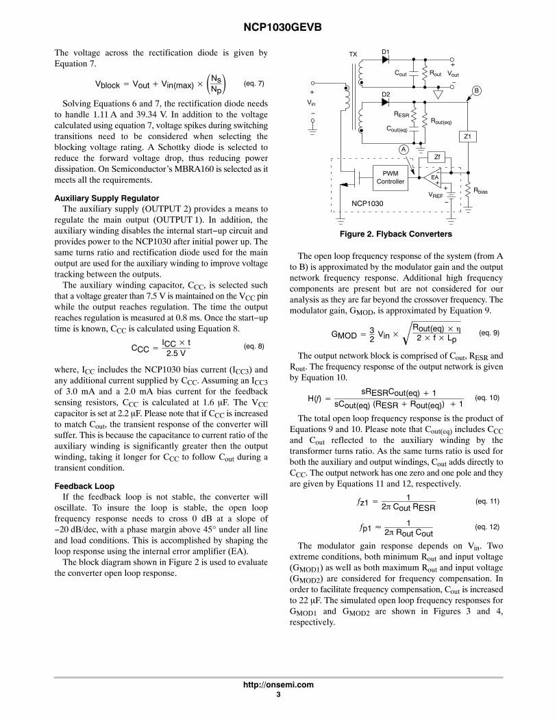
oscillate. To insure the loop is stable, the open loopfrequency response needs to cross 0 dB at a slope of−20 dB/dec, with a phase margin above 45° under all lineand load conditions. This is accomplished by shaping theloop response using the internal error amplifier (EA).
The block diagram shown in Figure 2 is used to evaluatethe converter open loop response.
Figure 2. Flyback Converters
TX
D2
+
−
EAPWM
Controller
+
−
A
+
−
D1
+
−
Z1
B
Vin
Cout Rout Vout
RESR
Cout(eq)
Rout(eq)
NCP1030VREF
Zf
Rbias
The open loop frequency response of the system (from Ato B) is approximated by the modulator gain and the outputnetwork frequency response. Additional high frequencycomponents are present but are not considered for ouranalysis as they are far beyond the crossover frequency. Themodulator gain, GMOD, is approximated by Equation 9.
GMOD � 32
Vin �Rout(eq) � �2 � f � Lp
(eq. 9)
The output network block is comprised of Cout, RESR andRout. The frequency response of the output network is givenby Equation 10.
H(f) �sRESRCout(eq) � 1
sCout(eq) (RESR � Rout(eq)) � 1(eq. 10)
The total open loop frequency response is the product ofEquations 9 and 10. Please note that Cout(eq) includes CCCand Cout reflected to the auxiliary winding by thetransformer turns ratio. As the same turns ratio is used forboth the auxiliary and output windings, Cout adds directly toCCC. The output network has one zero and one pole and theyare given by Equations 11 and 12, respectively.
fz1 � 12� Cout RESR
(eq. 11)
fp1 12� Rout Cout
(eq. 12)
The modulator gain response depends on Vin. Twoextreme conditions, both minimum Rout and input voltage(GMOD1) as well as both maximum Rout and input voltage(GMOD2) are considered for frequency compensation. Inorder to facilitate frequency compensation, Cout is increasedto 22 �F. The simulated open loop frequency responses forGMOD1 and GMOD2 are shown in Figures 3 and 4,respectively.
NCP1030GEVB
http://onsemi.com4
Figure 3. Open Loop Frequency Response for GMOD1
−50
−40
−30
−20
−10
0
10
20
30
40
50
Frequency (Hz)
Mag
nitu
de (
dB)
−100
−90
−80
−70
−60
−50
−40
−30
−20
−10
0
Ang
le (
degr
ees)
101 102 103 104 105 106
MagnitudePhase
Figure 4. Open Loop Frequency Response for GMOD2
101 102 103 104 105 106−50
−40
−30
−20
−10
0
10
20
30
40
50
Frequency (Hz)
Mag
nitu
de (
dB)
−100
−90
−80
−70
−60
−50
−40
−30
−20
−10
0
Ang
le (
degr
ees)
MagnitudePhase
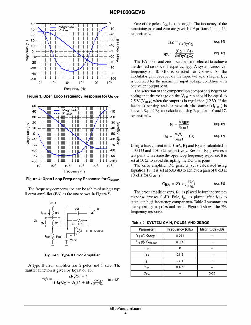
The frequency compensation can be achieved using a typeII error amplifier (EA) as the one shown in Figure 5.
Figure 5. Type II Error Amplifier
+
−
+
−
C2 R7
C6R6
R4
Zf
Z1
Input
Output
(R5)
EA
Ibias1
RbiasVREF
A type II error amplifier has 2 poles and 1 zero. Thetransfer function is given by Equation 13.
H(f) �sR7C2 � 1
sR4(C2 � C6)�1 � sR7C7C6
C7�C6� (eq. 13)
One of the poles, fp2, is at the origin. The frequency of theremaining pole and zero are given by Equations 14 and 15,respectively.
fz2 � 12�R7C2
(eq. 14)
fp3 �(C2 � C6)2�R7C2C6
(eq. 15)
The EA poles and zero locations are selected to achievethe desired crossover frequency, fCO. A system crossoverfrequency of 10 kHz is selected for GMOD1. As themodulator gain depends on the input voltage, a higher fCOis obtained for the maximum input voltage condition withequivalent output load.
The selection of the compensation components begins bynoting that the voltage on the VFB pin should be equal to2.5 V (VREF) when the output is in regulation (12 V). If thefeedback sensing resistor network bias current (Ibias1) isknown, R4 and R5 are calculated using Equations 16 and 17,respectively.
R5 �VREFIbias1
(eq. 16)
R4 �VCCIbias1
� R5 (eq. 17)
Using a bias current of 2.0 mA, R4 and R5 are calculated at4.99 k� and 1.30 k�, respectively. Resistor R6 provides atest point to measure the open loop frequency response. It isset at 10�� to avoid disrupting the DC bias point.
The error amplifier DC gain, GEA, is calculated usingEquation 18. It is set at 6.03 dB to achieve a gain of 0 dB at10 kHz for GMOD1.
GEA � 20 log�R7R4� (eq. 18)
The error amplifier zero, fz2, is placed before the systemresponse crosses 0 dB. Pole, fp3, is placed after fCO toattenuate high frequency components. Table 3 summarizesthe system gain, poles and zeros. Figure 6 shows the EAfrequency response.
Table 3. SYSTEM GAIN, POLES AND ZEROS
Parameter Frequency (kHz) Magnitude (dB)
fP1 (@ GMOD1) 0.091 −
fP1 (@ GMOD2) 0.009 −
fP2 0 −
fP3 23.9 −
fZ1 77.4 −
fZ2 0.482 −
GEA − 6.03
NCP1030GEVB
http://onsemi.com5
Figure 6. Error Amplifier Frequency Response
101 102 103 104 105 106
−40
−30
−20
−10
0
10
20
30
40
50
60
Frequency (Hz)
Mag
nitu
de (
dB)
−100
−90
−80
−70
−60
−50
−40
−30
−20
−10
0
Ang
le (
degr
ees)
MagnitudePhase
The phase contributions of a zero and a pole at thecrossover frequency are given by Equations 19 and 20,respectively.
�z � tan−1�fCOfz� (eq. 19)
�p � tan−1�fCOfp� (eq. 20)
The phase margin, �M, is evaluated taking into account thephase contribution of all the poles and zeros as shown belowin Equation 21.
�M � 180 � �p1 � �p2 � �p3 � �z1 � �z2 (eq. 21)°
�M � 180 � 89.5 � 90 � 22.7 � 7.33 � 87.24 � 72.4° ° ° ° ° ° °
The calculated phase margin is 72.4°. The 180° termarises because the EA is in an inverting configuration. Thesimulated system frequency responses for GMOD1 andGMOD2 are shown in Figure 7.
101 102 103 104 105 106−20
−10
0
10
20
30
40
50
60
70
80
Frequency (Hz)
Mag
nitu
de (
dB)
−180
−170
−160
−150
−140
−130
−120
−110
−100
−90
−80
Ang
le (
degr
ees)
Magnitude(Vin = 36V,Rout = 72�)
Phase(Vin = 36V,Rout = 72�)
Magnitude(Vin = 76V,Rout = 720�)
Phase(Vin = 76V,Rout = 720�)
Figure 7. System Frequency Response
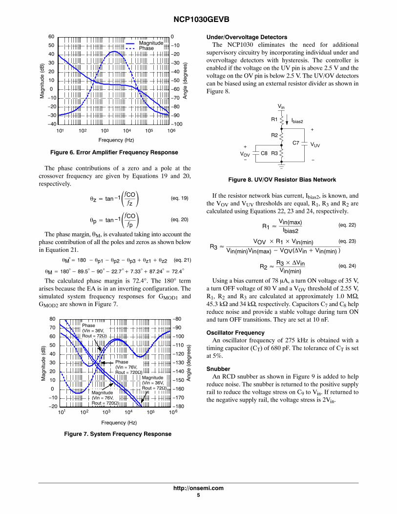
Under/Overvoltage DetectorsThe NCP1030 eliminates the need for additional
supervisory circuitry by incorporating individual under andovervoltage detectors with hysteresis. The controller isenabled if the voltage on the UV pin is above 2.5 V and thevoltage on the OV pin is below 2.5 V. The UV/OV detectorscan be biased using an external resistor divider as shown inFigure 8.
Figure 8. UV/OV Resistor Bias Network
R1
+
−
R2
R3
+
−
C7
C8
Vin
Ibias2
VUV
VOV
If the resistor network bias current, Ibias2, is known, andthe VOV and VUV thresholds are equal, R1, R3 and R2 arecalculated using Equations 22, 23 and 24, respectively.
R1 Vin(max)
Ibias2(eq. 22)
R3 VOV � R1 � Vin(min)
Vin(min)Vin(max) � VOV(Vin � Vin(min) )
(eq. 23)
R2 R3 � Vin
Vin(min)(eq. 24)
Using a bias current of 78 �A, a turn ON voltage of 35 V,a turn OFF voltage of 80 V and a VOV threshold of 2.55 V,R1, R2 and R3 are calculated at approximately 1.0 M�,45.3 k� and 34 k�, respectively. Capacitors C7 and C8 helpreduce noise and provide a stable voltage during turn ONand turn OFF transitions. They are set at 10 nF.
Oscillator FrequencyAn oscillator frequency of 275 kHz is obtained with a
timing capacitor (CT) of 680 pF. The tolerance of CT is setat 5%.
SnubberAn RCD snubber as shown in Figure 9 is added to help
reduce noise. The snubber is returned to the positive supplyrail to reduce the voltage stress on C9 to Vin. If returned tothe negative supply rail, the voltage stress is 2Vin.
NCP1030GEVB
http://onsemi.com6
Figure 9. RCD Snubber
TX
D3 R9
C9
Vin
+
−
The power dissipation of R9 is determined by C9 and isgiven by equation 25.
(eq. 25)P � 12
C9 Vin2 f
The snubber components are not assembled in theconverter. However, electrical connections are provided ifthe user wants to add the snubber components.
Input FilterAn L−C filter at the converter input is used to reduce EMI.
The input L−C filter reduces noise and provides a solid inputvoltage to the converter. The filter is shown in Figure 10.Capacitor C10 is used for common mode noise reduction.
Figure 10. Input L−C Filter Schematic
L1
C5 2.2
+
−
C10 0.022
Vin
2.2 �H
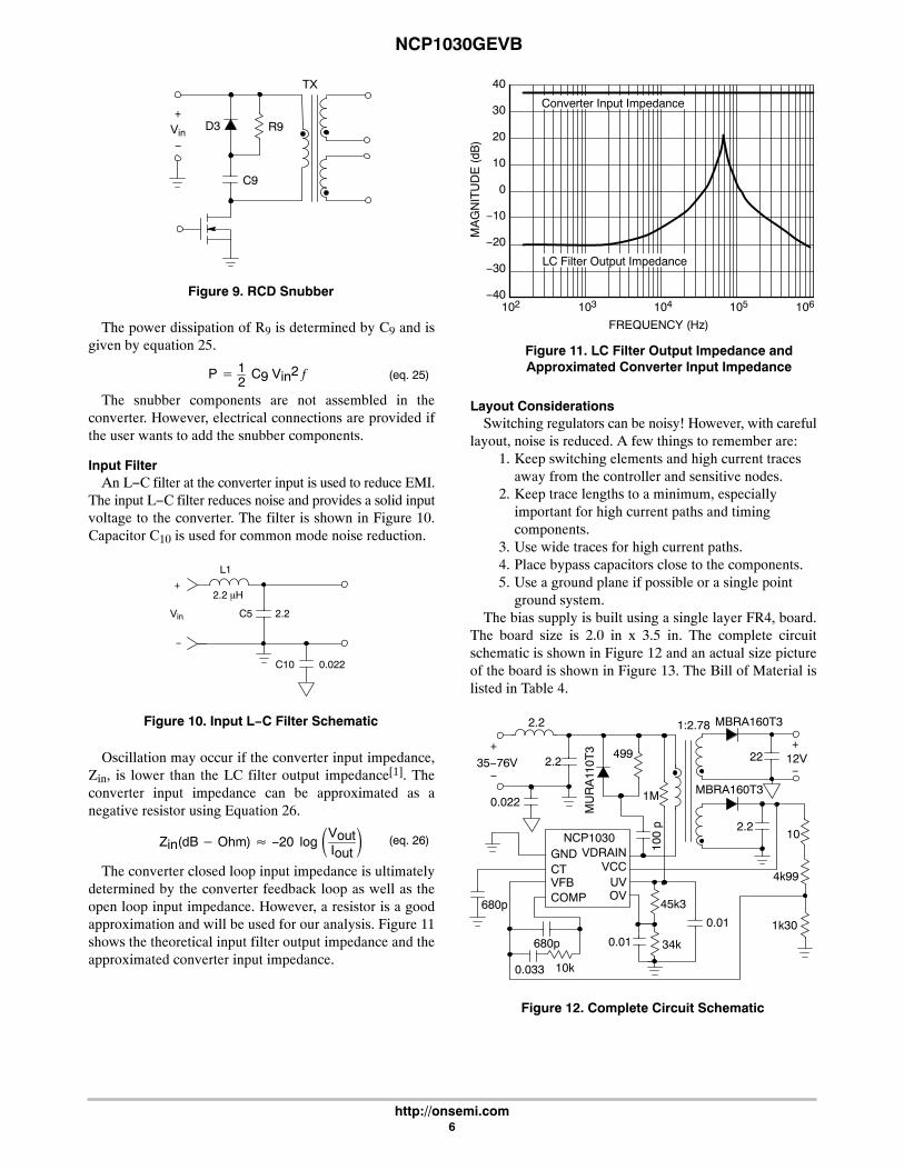
Oscillation may occur if the converter input impedance,Zin, is lower than the LC filter output impedance[1]. Theconverter input impedance can be approximated as anegative resistor using Equation 26.
Zin(dB � Ohm) −20 log �VoutIout� (eq. 26)
The converter closed loop input impedance is ultimatelydetermined by the converter feedback loop as well as theopen loop input impedance. However, a resistor is a goodapproximation and will be used for our analysis. Figure 11shows the theoretical input filter output impedance and theapproximated converter input impedance.
Figure 11. LC Filter Output Impedance andApproximated Converter Input Impedance
LC Filter Output Impedance
Converter Input Impedance
40
30
20
10
0
−10
−20
−30
−40102 103 104 105 106
FREQUENCY (Hz)
MA
GN
ITU
DE
(dB
)
Layout ConsiderationsSwitching regulators can be noisy! However, with careful
layout, noise is reduced. A few things to remember are:1. Keep switching elements and high current traces
away from the controller and sensitive nodes.2. Keep trace lengths to a minimum, especially
important for high current paths and timingcomponents.
3. Use wide traces for high current paths.4. Place bypass capacitors close to the components.5. Use a ground plane if possible or a single point
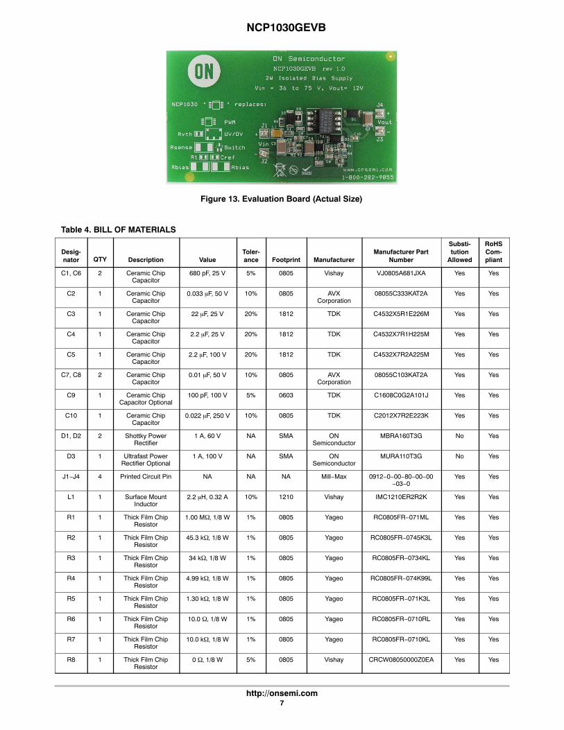
ground system.The bias supply is built using a single layer FR4, board.
The board size is 2.0 in x 3.5 in. The complete circuitschematic is shown in Figure 12 and an actual size pictureof the board is shown in Figure 13. The Bill of Material islisted in Table 4.
Figure 12. Complete Circuit Schematic
GND
COMP
+
35−76V−
VCCVDRAIN
UVOV
CTVFB
+
−22
MBRA160T3
MBRA160T3
2.2
1M
10
4k99
1k30
10k0.033
680p
680p
0.01
0.01
2.2
2.2
1:2.78
45k3
34k
12V
NCP1030
0.022
100
p
MU
RA
110T
3 499
NCP1030GEVB
http://onsemi.com7
Figure 13. Evaluation Board (Actual Size)
Table 4. BILL OF MATERIALS
Desig-nator QTY Description Value
Toler-ance Footprint Manufacturer
Manufacturer PartNumber
Substi-tution
Allowed
RoHSCom-pliant
C1, C6 2 Ceramic ChipCapacitor
680 pF, 25 V 5% 0805 Vishay VJ0805A681JXA Yes Yes
C2 1 Ceramic ChipCapacitor
0.033 �F, 50 V 10% 0805 AVXCorporation
08055C333KAT2A Yes Yes
C3 1 Ceramic ChipCapacitor
22 �F, 25 V 20% 1812 TDK C4532X5R1E226M Yes Yes
C4 1 Ceramic ChipCapacitor
2.2 �F, 25 V 20% 1812 TDK C4532X7R1H225M Yes Yes
C5 1 Ceramic ChipCapacitor
2.2 �F, 100 V 20% 1812 TDK C4532X7R2A225M Yes Yes
C7, C8 2 Ceramic ChipCapacitor
0.01 �F, 50 V 10% 0805 AVXCorporation
08055C103KAT2A Yes Yes
C9 1 Ceramic ChipCapacitor Optional
100 pF, 100 V 5% 0603 TDK C1608C0G2A101J Yes Yes
C10 1 Ceramic ChipCapacitor
0.022 �F, 250 V 10% 0805 TDK C2012X7R2E223K Yes Yes
D1, D2 2 Shottky PowerRectifier
1 A, 60 V NA SMA ONSemiconductor
MBRA160T3G No Yes
D3 1 Ultrafast PowerRectifier Optional
1 A, 100 V NA SMA ONSemiconductor
MURA110T3G No Yes
J1−J4 4 Printed Circuit Pin NA NA NA Mill−Max 0912−0−00−80−00−00−03−0
Yes Yes
L1 1 Surface MountInductor
2.2 �H, 0.32 A 10% 1210 Vishay IMC1210ER2R2K Yes Yes
R1 1 Thick Film ChipResistor
1.00 M�, 1/8 W 1% 0805 Yageo RC0805FR−071ML Yes Yes
R2 1 Thick Film ChipResistor
45.3 k�, 1/8 W 1% 0805 Yageo RC0805FR−0745K3L Yes Yes
R3 1 Thick Film ChipResistor
34 k�, 1/8 W 1% 0805 Yageo RC0805FR−0734KL Yes Yes
R4 1 Thick Film ChipResistor
4.99 k�, 1/8 W 1% 0805 Yageo RC0805FR−074K99L Yes Yes
R5 1 Thick Film ChipResistor
1.30 k�, 1/8 W 1% 0805 Yageo RC0805FR−071K3L Yes Yes
R6 1 Thick Film ChipResistor
10.0 �, 1/8 W 1% 0805 Yageo RC0805FR−0710RL Yes Yes
R7 1 Thick Film ChipResistor
10.0 k�, 1/8 W 1% 0805 Yageo RC0805FR−0710KL Yes Yes
R8 1 Thick Film ChipResistor
0 �, 1/8 W 5% 0805 Vishay CRCW08050000Z0EA Yes Yes
NCP1030GEVB
http://onsemi.com8
Table 4. BILL OF MATERIALS
Desig-nator
RoHSCom-pliant
Substi-tution
AllowedManufacturer Part
NumberManufacturerFootprintToler-anceValueDescriptionQTY
R9 1 Thick Film ChipResistor Optional
499 �, 1/3 W 1% 1210 Vishay CRCW1210499RFKEA Yes Yes
TX1 1 FlybackTransformer
120 �H, 12 V 10% 10.16 x12.07 mm
Coilcraft B0226−EL Yes Yes
U1 1 PWM Controller NA NA Micro8 ONSemiconductor
NCP1030DMR2G No Yes
Design VerificationThe final step in our design includes validation and test of
the bias supply. Before powering the supply, it should beinspected for potential problems. A few suggestionsinclude:
1. Verify all connections. Check for shorts and opens,especially on the input and output terminals.
2. Verify component values.3. Slowly increase the input voltage while
monitoring the input current. If the input currentexceeds 10 mA, repeat steps 1 to 3.
4. Once the input voltage reaches 25 V, measure thevoltage on critical nodes. The NCP1030 start−upregulator should be ON. If the voltages are notcorrect, remove power and repeat steps 1 to 3.
5. Increase the input voltage to 36 V. Measure theoutput voltage. If it is not approximately 12 V,repeat steps 1 to 3.
6. Increase the input voltage above 80 V. The outputshould turn OFF.
Please be careful when probing and testing the converter.High voltage may be present. Exercise CAUTION!
Once the converter functionality is verified, the boardperformance is evaluated and compared to our originalgoals. The evaluation criteria includes:
1. Open loop frequency response.2. Efficiency.3. Line and load regulation.4. Step load response.5. Start−up response.
The open loop response is measured injecting an ACsignal across R6 using a network analyzer as shown inFigure 14.
Figure 14. Open Loop Frequency ResponseMeasurement Set−up
D2
+
−
Z11:1
R6
NetworkAnalyzer
REF
A
B
To Converter
To ErrorAmplifier
CCC VCC
Rbias
The measured frequency response is shown in Figure 15.The crossover frequency is measured at 9 kHz.
Figure 15. Open Loop Frequency Response
50
Mag
nitu
de (
dB)
40
30
20
10
0
−10
−20
−30
−40
−50102 103 104 105 106
Frequency (Hz)
Vin = 36 VRout = 72 �
NCP1030GEVB
http://onsemi.com9
Peak efficiency is measured at 83%. Figure 16 shows theefficiency vs. output current under several input voltageconditions.
Figure 16. Efficiency vs Output Current
Iout, OUTPUT CURRENT (mA)
125
85
50
70
250
�, E
ffici
ency
(%
)
60
90
65
75
80
20075 100 150 175
Vin = 36V
Vin = 48V
Vin = 76V
Line and load regulation are calculated usingEquations 27 and 28, respectively.
RegLINE �VoutVin
(eq. 27)
RegLOAD �Vout(No Load) � Vout(Full Load)
Vout(No Load)(eq. 28)
Line regulation is measured below 0.5% and loadregulation is measured below 8%. Figure 17 shows theoutput voltage variation to output current under severalinput voltage conditions.
Figure 17. Output Voltage vs. Output Current
Iout, OUTPUT CURRENT (mA)
125
11.9
50
11.2
250
Vou
t, O
utpu
t Vol
tage
(V
)
11.0
12.0
11.1
11.7
11.8
20075 100 150 175
11.3
11.4
11.5
11.6
Vin = 36V
Vin = 48VVin = 76V
The dynamic response of the converter is evaluatedstepping the load current from 50% to 75% and from 75%to 50% of Iout(max). The step load transient responses areshown in Figures 18 and 19.
Figure 18. Output Voltage Response to aStep Load from 87 mA to 127 mA
Vin = 48 V
Vout = 11.6 V
50 ms/DIV
Vou
t, O
utpu
t Vol
tage
(50
mV
/DIV
)I o
ut, O
utpu
t Cur
rent
(20
mA
/DIV
)
Iout = 87 mA
Figure 19. Output Voltage Response to aStep Load from 127 mA to 87 mA
Vin = 48 V
Iout = 127 mA
Vout = 11.45 V
50 ms/DIV
Vou
t, O
utpu
t Vol
tage
(50
mV
/DIV
)I o
ut, O
utpu
t Cur
rent
(20
mA
/DIV
)
Output voltage ripple is measured at 25 mV for an outputcurrent of 170 mA. It is significantly below the 50 mVtarget. The output voltage ripple waveform is shown inFigure 20.

NCP1030GEVB
http://onsemi.com10
Vin = 48 V
Vout = 11.33 V
2.0 �s/DIV
Vou
t, O
utpu
t Vol
tage
(20
mV
/DIV
)
Figure 20. Output Voltage Ripple
Iout = 170 mA
Finally, the converter turn ON response at full load isevaluated. Figure 21 shows the output turn ON transientresponse at full load.
OUTPUT2
1.0 ms/DIV
Vou
t, O
utpu
t Vol
tage
(2.
0 V
/DIV
)
Figure 21. Output Voltage During Turn ONat Full Load
Iout = 170 mA
OUTPUT1 (Isolated)
0 V
DSS Operation
Output 2 operates in DSS while the converter is disabled.Once the converter is enabled, Output 1 tracks Output 2.
SummaryAn isolated 12 V bias supply for a 48 V telecom system is
implemented using the NCP1030. The converter achieves apeak efficiency of 83% while providing good transientresponse.
References1. Ridley, Ray. “The Evolution of Power Electronics’’,
Switching Power Magazine, Fall 2001:16−30.2. Pressman, Abraham I. Switching Power Supply
Design. 2nd ed. New York, NY: MacGraw Hill.
NCP1030GEVB
http://onsemi.com11
TEST PROCEDURE FOR THE NCP1030GEVB
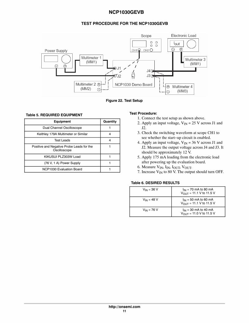
Figure 22. Test Setup
Table 5. REQUIRED EQUIPMENT
Equipment Quantity
Dual Channel Oscilloscope 1
Keithley 179A Multimeter or Similar 4
Test Leads 4
Positive and Negative Probe Leads for theOscilloscope
1
KIKUSUI PLZ303W Load 1
(76 V, 1 A) Power Supply 1
NCP1030 Evaluation Board 1
Test Procedure:1. Connect the test setup as shown above.2. Apply an input voltage, VIN = 25 V across J1 and
J2.3. Check the switching waveform at scope CH1 to
see whether the start−up circuit is enabled.4. Apply an input voltage, VIN = 36 V across J1 and
J2. Measure the output voltage across J4 and J3. Itshould be approximately 12 V.
5. Apply 175 mA loading from the electronic loadafter powering up the evaluation board.
6. Measure VIN, IIN, IOUT, VOUT.7. Increase VIN to 80 V. The output should turn OFF.
Table 6. DESIRED RESULTS
VIN = 36 V IIN = 70 mA to 80 mAVOUT = 11.1 V to 11.5 V
VIN = 48 V IIN = 50 mA to 60 mAVOUT = 11.1 V to 11.5 V
VIN = 76 V IIN = 30 mA to 40 mAVOUT = 11.0 V to 11.5 V

www.onsemi.com1
onsemi, , and other names, marks, and brands are registered and/or common law trademarks of Semiconductor Components Industries, LLC dba “onsemi” or its affiliatesand/or subsidiaries in the United States and/or other countries. onsemi owns the rights to a number of patents, trademarks, copyrights, trade secrets, and other intellectual property. Alisting of onsemi’s product/patent coverage may be accessed at www.onsemi.com/site/pdf/Patent−Marking.pdf. onsemi is an Equal Opportunity/Affirmative Action Employer. Thisliterature is subject to all applicable copyright laws and is not for resale in any manner.
The evaluation board/kit (research and development board/kit) (hereinafter the “board”) is not a finished product and is not available for sale to consumers. The board is only intendedfor research, development, demonstration and evaluation purposes and will only be used in laboratory/development areas by persons with an engineering/technical training and familiarwith the risks associated with handling electrical/mechanical components, systems and subsystems. This person assumes full responsibility/liability for proper and safe handling. Anyother use, resale or redistribution for any other purpose is strictly prohibited.
THE BOARD IS PROVIDED BY ONSEMI TO YOU “AS IS” AND WITHOUT ANY REPRESENTATIONS OR WARRANTIES WHATSOEVER. WITHOUT LIMITING THE FOREGOING,ONSEMI (AND ITS LICENSORS/SUPPLIERS) HEREBY DISCLAIMS ANY AND ALL REPRESENTATIONS AND WARRANTIES IN RELATION TO THE BOARD, ANYMODIFICATIONS, OR THIS AGREEMENT, WHETHER EXPRESS, IMPLIED, STATUTORY OR OTHERWISE, INCLUDING WITHOUT LIMITATION ANY AND ALLREPRESENTATIONS AND WARRANTIES OF MERCHANTABILITY, FITNESS FOR A PARTICULAR PURPOSE, TITLE, NON−INFRINGEMENT, AND THOSE ARISING FROM ACOURSE OF DEALING, TRADE USAGE, TRADE CUSTOM OR TRADE PRACTICE.
onsemi reserves the right to make changes without further notice to any board.
You are responsible for determining whether the board will be suitable for your intended use or application or will achieve your intended results. Prior to using or distributing any systemsthat have been evaluated, designed or tested using the board, you agree to test and validate your design to confirm the functionality for your application. Any technical, applications ordesign information or advice, quality characterization, reliability data or other services provided by onsemi shall not constitute any representation or warranty by onsemi, and no additionalobligations or liabilities shall arise from onsemi having provided such information or services.
onsemi products including the boards are not designed, intended, or authorized for use in life support systems, or any FDA Class 3 medical devices or medical devices with a similaror equivalent classification in a foreign jurisdiction, or any devices intended for implantation in the human body. You agree to indemnify, defend and hold harmless onsemi, its directors,officers, employees, representatives, agents, subsidiaries, affiliates, distributors, and assigns, against any and all liabilities, losses, costs, damages, judgments, and expenses, arisingout of any claim, demand, investigation, lawsuit, regulatory action or cause of action arising out of or associated with any unauthorized use, even if such claim alleges that onsemi wasnegligent regarding the design or manufacture of any products and/or the board.
This evaluation board/kit does not fall within the scope of the European Union directives regarding electromagnetic compatibility, restricted substances (RoHS), recycling (WEEE), FCC,CE or UL, and may not meet the technical requirements of these or other related directives.
FCC WARNING – This evaluation board/kit is intended for use for engineering development, demonstration, or evaluation purposes only and is not considered by onsemi to be a finishedend product fit for general consumer use. It may generate, use, or radiate radio frequency energy and has not been tested for compliance with the limits of computing devices pursuantto part 15 of FCC rules, which are designed to provide reasonable protection against radio frequency interference. Operation of this equipment may cause interference with radiocommunications, in which case the user shall be responsible, at its expense, to take whatever measures may be required to correct this interference.
onsemi does not convey any license under its patent rights nor the rights of others.
LIMITATIONS OF LIABILITY: onsemi shall not be liable for any special, consequential, incidental, indirect or punitive damages, including, but not limited to the costs of requalification,delay, loss of profits or goodwill, arising out of or in connection with the board, even if onsemi is advised of the possibility of such damages. In no event shall onsemi’s aggregate liabilityfrom any obligation arising out of or in connection with the board, under any theory of liability, exceed the purchase price paid for the board, if any.
The board is provided to you subject to the license and other terms per onsemi’s standard terms and conditions of sale. For more information and documentation, please visitwww.onsemi.com.
PUBLICATION ORDERING INFORMATIONTECHNICAL SUPPORTNorth American Technical Support:Voice Mail: 1 800−282−9855 Toll Free USA/CanadaPhone: 011 421 33 790 2910
LITERATURE FULFILLMENT:Email Requests to: [email protected]
onsemi Website: www.onsemi.com
Europe, Middle East and Africa Technical Support:Phone: 00421 33 790 2910For additional information, please contact your local Sales Representative
◊