Embed Size (px)
Citation preview

Active and Passive Elec. Comp., 1992, Vol. 14, pp. 245-249Reprints available directly from the publisherPhotocopying permitted by license only() 1992 Gordon and Breach Science Publishers S.A.
Printed in the United Kingdom
EVAPORATION OF ADHERENT AI-FILMS ONSINGLE CRYSTALLINE LiNbO3 SUBSTRATES
E. SCHIPPELDepartment of Electrotechnics, Technical University 0-2400 Wismar, Germany
LiNbO3 is used as a single crystalline substrate material for the manufacturing of surface acoustic wavedevices as frequency selective components. On the polished substrate wafer, AI with a film thicknessof about 400 nm is evaporated in a high vacuum.
The difficulties of the inadequate adhesion of the structured Al-film were eliminated by systematicalinvestigations. Films that were adherent to the total surface could be prepared by evaporating anintermediate film of Cr or SiOx or, otherwise, a mixed film of AI with Si.
An ultrasonic test for adhesion strength was developed that results in an assessment of local andalso large-area film adhesion.
I. INTRODUCTION
For electronics, Lithium niobate (LiNbO3) is a very interesting material. Becauseof its crystal class 3m, LiNbO3 is trigonal and polar. It is a ferroelectric materialwith large pyroelectric, piezoelectric, electro-optic, and photo-elastic coefficients.Therefore, static electric charges may occur on the substrate surface because oftemperature variations. A detailed description of the crystal structure and thephysical characteristics of the LiNbO3 are given by WEIS and GAYLORD1.
The growth of the LiNbO3 single crystals can be made by the Czochralski method.To avoid areas of different polarity in a crystal, the polarity during the growing ofa crystal above the Curie-temperature of 1140C can be set by an electric field2,3.A field of application of LiNbO3 is the manufacturing of surface acoustic wave
devices. For that purpose a metal film is evaporated onto a polished single crystallinesubstrate wafer in high vacuum. An interdigital structure is then generated bymeans of photolithography. The interdigital structure consists of two "combs" ofdifferent shape and size. The structural widths of electrodes of the interdigitalstructure are less than 15 tm. The frequency range of the filters depends on thestructural width; frequencies of more than 300 MHz require electrode widths ofabout 1/zm. The electrical contact is created by bonding of Al-wires to the structuredmetal film.A good adhesion strength of the evaporated metal film on the vibrating surface
is absolutely necessary for the function of the filters. Concerning the yz cut therewere problems of adhesion bonds with the 38-cut.
245

246 E. SCHIPPEL
II. EXPERIMENT
In production, the polished LiNbO3 wafers are given a short treatment with variouschemicals. Therefore, tests of various pretments of the LiNbO3 wafers were made.After a standard cleaning with acetone in an ultrasonic bath, the wafers were treatedat 20C and 50C for 5 min and 20 min with the following chemicals:
1. NH3 HF, 20% solvent2. Chromium-sulphuric acid3. NaOH, 20% solvent4. H3 PO4, concentrated solvent5. H2 F2, concentrated solvent
An assessment of the efficiency of the chemicals with respect to the surface ofLiNbO3 wafers resulted from electron microscopic photographs.
In another test series, standardized cleaned and pre-treated glass and LiNbO3substrates were coated under the same conditions with A1 by evaporization. Thesetests should show differences between the adhesion of A1 films to amorphous glassand crystalline LiNbO3.
In general, the evaporation was done from W-boats on the substrates in vacuumwith and without a glow discharge. For the manufacturing of a mixed film, AI andthe additives Cu, Si and Ni were evaporated from separate boats. The thicknessof the mixed film was 20 nm to 50 nm. Above it, pure A1 was evaporated up to athickness of 400 nm.
For the manufacturing of intermediate films, SiOx as an insulator or Cr as ametal were first evaporated to a maximum thickness of 30 nm, followed by pureAI evaporated up to a total thickness of 400 nm.
To investigate the adhesion of the evaporated films a test method was developed.The samples are immersed into a solvent (e.g., acetone, xylene) and ultrasonicallyagitated4. The test method is sensitive to the extent of adherence of the film to thesubstrate. The test method can be incorporated into a production process becauseit is non-distructive of fully adherent films.
By this test method, non-adherent or not sufficiently adherent films are removedfrom the substrate and visually obscure as spots without a film. By the properchoice of solvent for sound-transmission, ultrasonic frequency and treatment time,the test method can be adapted to the adhesion bond necessary for the product4.For the assessment of the investigations, a screen of 1 mm x 1 mm was used tomeasure the area of substrate without a film.
III. RESULTS
From electron microscopic investigations, the surface of the LiNbO3 wafer appearsto be affected in different ways by different chemicals. There is no surface effectdue to NH3 HE The largest etching pits, which are arranged according to the crystalsymmetry, are produced by H2 F2. Fig. 1 shows the classification of the chemicals

EVAPORATION OF ADHERENT AI-FILMS 247
Effect of Etching
1 2 3 4 5
FIGURE Classification of chemicals according to the etching effect on the LiNbO3 wafer.lmNH3 HF (20% solvent),2mChromium-sulphuric acid3--NaOH (concentrated solvent)4---H3 PO4 (concentrated solvent)5--H_, F2 (concentrated solvent).
according to the etching effect on the LiNbO3 wafer. It was found that the treat-ments of the LiNbO3 wafer with chromium-sulphuric acid and H3 PO4 will improvethe adhesion of the A1 film.
Fig. 2 shows clearly that the adhesion of the A1 film is essentially worse onLiNbO3 than on glass. After a test time of 10 min the A1 film has been nearly 60%dissolved from the LiNbO3, while it is still on the glass surface up to more than90%.
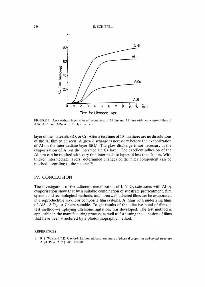
For the film systems with an underlying film on the substrate, it was found thatthe adhesion of the A1 film along with an A1Si mixed film is excellent as Fig. 3shows. AI films with an underlying mixed film of A1Cu have better adhesion thanwith AINi mixed films or films of pure AI. To retain the filter function of thecomponent, the thickness of the mixed film must not succeed 30 to 40 nm5.An excellent adhesion is also to be found with the A1 films with an intermediate
6O
2O
Substrate
’1 2 3 4 5 6 7 8 9 10Time for Ultn3scic Test rain
FIGURE 2 Area without layer after ultrasonic test of pure AI film on glass- and LiNbO3-substrate inpercent.
248 E. SCHIPPEL
8O AINi
6O
AtCu
0 2 3 z, 5 6 7 9, 10 min
Time for Ultrasonic Test
FIGURE 3 Area without layer after ultrasonic test of AI film and AI films with below mixed films ofAISi, AICu and AINi on LiNbO3 in percent.
layer of the materials SiOx or Cr. After a test time of 10 min there are no dissolutionsof the A1 film to be seen. A glow discharge is necessary before the evaporizationof A1 on the intermediate layer SiOx6. The glow discharge is not necessary at theevaporization of A1 on the intermediate Cr layer. The excellent adhesion of theAI film can be reached with very thin intermediate layers of less than 20 nm. Withthicker intermediate layers, determined changes of the filter component can bereached according to the patents7,8.
IV. CONCLUSION
The investigation of the adherent metallization of LiNbO3 substrates with A1 byevaporization show that by a suitable combination of substrate pretreatment, filmsystem, and technological methods, total-area well-adhered films can be evaporatedin a reproductible way. For composite film systems, AI films with underlying filmsof A1Si, SiOx, or Cr are suitable. To get results of the adhesive bond of films, atest methodemploying ultrasonic agitation, was developed. The test method isapplicable in the manufacturing process, as well as for testing the adhesion of filmsthat have been structured by a photolithographic method.
REFERENCES
1. R.S. Weis and T.K. Gaylord: Lithium niobate: summary of physical properties and crystal structureAppl. Phys. A37 (1985) 191-203.

EVAPORATION OF ADHERENT AI-FILMS 249
2. P.W. Haycock and P.D. Townsend: A method of poling LiNbO3 and LiTaO3 below Tc Appl. Phys.48 (1986) 698-700.
3. P. Reiche, J. Bohm, B. Hermoneit, P. Rudolph and D. Schulze: Wachstumsmorphologie vonLiNbO3-Einkristallen bei der Ziichtung nach dem Czochralski-Ver-fahren unter der Einwirkungeines elektrischen Feldes Cryst. Res. Technology 23 (1988) 467-474.
4. E. Schippel and A. Piech: Verfahren zur Priifung der Haft-festigkeit von aufgedampften SchichtenPatent (application 1989)
5. E. Schippel, T. V61ker and A. Breitlauch: Schichtsystem zur haftfesten Metallisierung piezoelek-trischer Substratmaterialien Patent DD 276 697.
6. E. Schippel and M. Schmidt: Verfahren zur haftfesten Metal-lisierung von piezoelektrischen Ma-terialien Patent DD 264 943.
7. Akustisches Oberflichenwellenwandler-System Patent D 2238 925.9.8. Schallwandler for akustische Oberflichenwellen Patent D 2431 620.0.

International Journal of
AerospaceEngineeringHindawi Publishing Corporationhttp://www.hindawi.com Volume 2010
RoboticsJournal of
Hindawi Publishing Corporationhttp://www.hindawi.com Volume 2014
Hindawi Publishing Corporationhttp://www.hindawi.com Volume 2014
Active and Passive Electronic Components
Control Scienceand Engineering
Journal of
Hindawi Publishing Corporationhttp://www.hindawi.com Volume 2014
International Journal of
RotatingMachinery
Hindawi Publishing Corporationhttp://www.hindawi.com Volume 2014
Hindawi Publishing Corporation http://www.hindawi.com
Journal ofEngineeringVolume 2014
Submit your manuscripts athttp://www.hindawi.com
VLSI Design
Hindawi Publishing Corporationhttp://www.hindawi.com Volume 2014
Hindawi Publishing Corporationhttp://www.hindawi.com Volume 2014
Shock and Vibration
Hindawi Publishing Corporationhttp://www.hindawi.com Volume 2014
Civil EngineeringAdvances in
Acoustics and VibrationAdvances in
Hindawi Publishing Corporationhttp://www.hindawi.com Volume 2014
Hindawi Publishing Corporationhttp://www.hindawi.com Volume 2014
Electrical and Computer Engineering
Journal of
Advances inOptoElectronics
Hindawi Publishing Corporation http://www.hindawi.com
Volume 2014
The Scientific World JournalHindawi Publishing Corporation http://www.hindawi.com Volume 2014
SensorsJournal of
Hindawi Publishing Corporationhttp://www.hindawi.com Volume 2014
Modelling & Simulation in EngineeringHindawi Publishing Corporation http://www.hindawi.com Volume 2014
Hindawi Publishing Corporationhttp://www.hindawi.com Volume 2014
Chemical EngineeringInternational Journal of Antennas and
Propagation
International Journal of
Hindawi Publishing Corporationhttp://www.hindawi.com Volume 2014
Hindawi Publishing Corporationhttp://www.hindawi.com Volume 2014
Navigation and Observation
International Journal of
Hindawi Publishing Corporationhttp://www.hindawi.com Volume 2014
DistributedSensor Networks
International Journal of