Embed Size (px)
Citation preview

REVISiÓN REVISTA MEXICANA DE FíSICA 45 (6) 5)9-550
Evanescent microwave pro bes and microscopy
DICIEMBRE 1999
A. García- Valen zuelaLaboratorio de Óptica Aplicada, Ce1ltro de Instrumentos, Universidad Nacional Autónoma de México
Apartado posta/70-186, 04510 México, D.F., Mexico.e-mili!: ga ,[email protected]:
M. Tabib-AzarE/ce/rical Engineering and Computer Sciellce Departmcnf, Cm'e Western Resene University
10900 Euclid Av., Clevelalld OH 44106, USA
Recibido el 20 de agosto de 1999; aceptado el 9 de septiembre de 1999
Evanescent microwave probes have gained considerable auention recently. Thcse probcs can obtain rncasurements of the microwave propcr-l¡es of materials with a very high spatial resolution. By scanning the probc across the arca of ¡oterest ¡mages of the topography, subsurfncefeaturcs, or microwave parameters can be gencrated fm a large variety of materials. In this article, we review the development and presentstate ol' evanescent microwave probcs and their use in microscopy. \Ve formulate a simple model ol' an evanescent prohe and discuss its basicprincipies aod potential as a nondestructive testing tool fm a variety of applications. \Ve address important issues regarding the fundamentaldifferences with other electromagnctic probes, the spatial resolution, and the sensitivity to changes in the sample's parameters. \Ve summa.rize recent work on applications of these prohes with difl'erent materials. The present paper gives motivation and the basic tools for furtherresearch inlo applications and fundamental issues 01'these probes.
Keywords: Microwaves; evanescent fields; microscopy; characterization of materials
Las .sondas de microondas evanescentes han llamado considerablemente la atención recientemente. Estos instrumentos pueden obtener medi.ciones de las características de los materiales en el rango de las microondas con una alta resolución espacial. Haciendo un barrido de la sonda<l través del área de interés se pueden generar imágenes de la topografía, defectos sub-superficiales y de las propiedades del material a lafrecuencia de operación para una gran variedad de materiales. En este artículo, presentamos una revisión del desarrollo y el estado actual deeste tipo de instrumentos y su uso en microscopía. Formulamos un modelo sencillo de una sonda evanescente y discutimos su principio básicoy su potencial como herramienta de pruebas no destructivas en diferentes aplicaciones. Consideramos aspectos importantes referentes a lasdiferencias con otro tipo de sondas electromagnéticas, la resolución espacial, y la sensibilidad al camhio en las propiedades del material deprueba. Resumimos el trabajo reciente en cuanto a las aplicaciones de estas sondas con diferentes materiales. Este artículo pretende motivary dar las herramientas básicas para continuar la investigación en los aspectos fundamentales y las aplicaciones de estos instrumelllos.
Descriptores: Microondas; campos evanescentes; microscopía; caracterización de materiales
PAes: 07.57.-c; 07.79.-v; 07.07
1. Introduction
In the last lwo decades, there has been an increasing in.terest on the development of probe microscopy techniques.Aftcr lhe introuuctioll of lhe scanning tunneling microscopy
(STM) in 1982 [1,2], many olhcr importanllcchniqucs bascdon Ihe local interaction 01' a sharp tip anu samplc were pro-poseJ anJ some are still under investigation. These tech-niques incluJe atomic force [3,4], magnetic force [5], ther.mal [G], ion conduclancc [7], near-licld oplical [8], andcapacitancc [9] scanning microscopy. In particular. atomicforce microcopy has become very popular due to its poten.tial lo ¡mage with atomic resolution very diffcrent kinds ofsurfaces. Other prohe techniques which have drawn many rc-scarchcrs attenlion in latcr years is the scanning ncar-field op-
tical microscopc (NSOM) [10-15] and scanning capacitance
microscopy (SCM) [IG-19J. Evanescenl microwave pro bes
(EMP) have also been considcreJ recently ami at Ihc time,
lhe potential nf thesc EMP appears to he vcry promising with
a largcr spcclrum 01'applications. In facl, EMP may bc foundlo be rclaled lo NSOM and lo SCM.
Thc I¡mil rcsolution ol" near-field prohes is one ol" thernain issues. In conventional optical rnicroscopes, the spatialresolution limit is in the arder ofthe wavelength used. Specif-ically, the smallest rcsolvablc spacing between two pointsources is >./2 sin Q, where O' is the collection angle that theaperture subtends. This limit is known as the Abbe harrier,oc lhe Jiffraction-limited rcsolution, and is due to diffractionphenomena inherenl to the wave phenomena. Thus is "un-brcakablc". Howcvcr, l!lis limil only applies lo Ihe conven-lional way 01"imaging lIsing len ses. It does not apply to scan~ning near-lickl microscopes, since diffraction, in the strictsensc of lhe lerm, is not involved in the probe-sample intcr-action. Nevcrthelcss, lhe wavclcngth ofradiation does playarole in some cases, and a gooJ figure of merit of a microscopeil1\'olving some kind 01"wave phenomena, is the spatial res-olution in terms 01"lhe wavelength. However in sorne casessuch figure of merit is not useful; e.g., in capacitan ce andeieclroslatic tcchniques lhe wavclcngth is considered infinite.
540 A. GARCíA-VALENZUELA AND M. TABIB-AZAR
The I¡mil lo lhe spatial resolution in a near ficld micro-scope has lo do more with lhe possibility to confine power!lux through a small arca (Ihc lip). Wavelenglh mayor maynol playa dominant role in such Iimit. Resolution, spatialor with rcspect lo changes on lhe sample propcrtics, depcndson lhe minimum detectable changc in lhe coupling bctwccnsamplc anu prohc.
2. Historie outline
Syngc is crcdited for suggcsting ror lhe first time near-Iicld microscopy [20] in 1928. E1ectromagnetic evanes-cenl fields werc considcrcd quantitativcly by Bcthc in cal-culating lhe coupling efficiency af microwavc wavcguidcslhrough a small apcrture much smaller than lhe wavelcngthin 1944 [21]. Baez uiscussed suh-wavelength resolulion anugavc a pmol' 01' principie experiment using an audio 05-
cillator in 1956 [221. The first experimental demonstmtion01' imaging with cvanescent t1elds at microwave frequencieswas carried out hy Soohoo in 1962 [23], anu in 1972 Ashand Nicholls uemonstrated that mierowave evanescent Heldsc(Julu he useu the image fealures on the order of .\/100 [24].
With the introduction of the scanning tunneling miero-scope (STM), Ihe technology to manipulate a small lip wilhsub-nanometer prccision evolved rapidly (being now com-mcrcially available). The present technology is bascd onpiezoelectric mieropositioners. Contrary to what one may ex-pecl, the technology is very simple (although costs can nothe overlookeu yet). An accessihle uescription of it is founuin the hook hy C. Julian Chen [25]. As inuicateu ahoye,STM and the scanning technology on an atomie-Ievel thatcame with il, triggered many to search for new probe tech-niques for microscopy based on different physical phenom-ena (atomie force, magnetic, aptical, ionic Iransport, elc.).In particular atomic force microscopy (AFM) soon followeuSTM [3,4,25]. heing hoth very popular touay. Alomic forcemicroscopy turned out to be more versatile, since Ihere is no!leed 01' a conducting sample, and is perhaps morc widelyused today. Elcctromagnetie probes at optical frequencieslúllowed rapidly. Pohl anu cuworkers reportcd an opticalslethoscopc with a spatial resolution appreciably less than lhewavelength in 1984 [8]. Their work staned few years hefore,anu a palcnt application preuates Ihe anicle [14]. In a scc-ond publication in 1986, they callcd their inslrumcnt a neur-lielu "plical scaiming microscope (NSOM) [lOJ. Their mi-croscope consisleu of u shurp quartz-tip covered wilh an alu-minum film with a smal! aperture al the apex. Independently,Lcwis and coworkers reported results of sub-wavelength res-olution in 1983 [11], and laler showeJ evanescent field im-ages 01' a gratin in 1996 L12]. Evanescent t¡eld rnicrowavepro bes wilh sub-wavelength resolution using a transmissiollline were considereJ in 1997 by Gutmann el al. ror planarslructure diagnosis [26], bUI no further works with MW 1'01-lowcd short aner. Since the mid 80's NSOM has caughl theattention of numerolls experimentalisls anu theoretieians, be-ing today a very active arca 01' research [15]. For a delailed
overview of diflerent types of NSOM whieh have been ex-plored, basic principies and instrumentation the reader is re-feneu tu the hook in ReL 13.
Scanning capacilancc microscopy (SCM) also fulloweuIhe inlroduction of Ihc STM [9,161. In 1989 Williams el al.reporteu a SCM on a 25 nm scale [17]. SCM consists ofmeasuring the capacilance betwecn a sharp tip and the sam-pIco High sensitivity to capacitance variations (rcsolution inthe arder of 1 x lO-HJ F) is achicved using a resonant cir-cuit [17-19]. The general chamcler of Ihe images ohlainedwilh a SCM is similar lo that of a STM hUIwith less spalialresolulion. However, in SCM Ihe sample may he covereu bya thin dielectric layer (maoy times this layer is forrned natM
urally aftcr exposure to air). This is a v¡rtuc of SCM in thatimaging of a conductor through a dielectric layer is possible.
Combinations of pro be mieroscopy tcchniqucs wcrc alsointroduccd. In particular SCM and AFM wcre combined in1991 hy Barret anu Quate [18]. They placed a conuucting lipon an AFM cantilever. Thc tip was pressed lo a lhin dielec-Irie layer forrncd on top ofthc conducting sample. Measuringdeftections of lhe cantilevcr gave in addition topographiealinformation uf the surfacc. The maio purpose of their instru-ment was lO measure thc charge storagc in a nitride-oxide-silicon system.
Evanescent rnierowavc probcs were again considercd un-til 1993 hy Tahih-Azar anu coworkers in [27]. A microstripquarter wavelcngth resonalor in conjunction with a smallprobe was uscd to Illap mierQwave conduclivity varialions inmetallic I¡nes on circuit boards and 01' a silicon wafer. Thepossibility of using electric dipole probcs as weIl as magnetiedipole pro bes in high rcsolution imaging was dernonstrated.Imaging of subsurface defects was shown to be feasible bydctecting hales in a printed circuit boaro that were coveredby solder ami werc not visible. Spatial rcsolution 011 the or-uer of .\/1000 was achieved. Since Ihen, other groups haveslarlcd working 011 EMP.
Xiang and coworkers reported in 1996 a scanning tipllcar-ficld microscopc al radio/microwavc frequencies. Thcmicroscope consistcd 01' a A/4 coaxial resonator with a ta-pcred center conductor, a sharpencd tip whieh is connected10 the ccnter conductor anJ protrudes from un aperture on ashielding plalc conllccted to the outer conductor. In their firstpublication a spatial resolution of 5 11m was reported (28). Ina slIbsequent puhlieation from the same laharatory, Gao et alreported an improved instrurnenl with a sharper tip achievinga 100 nm spatial resolution while imaging dielectric samples(corresponding to ,\/106). The tip was in soft contacl withthe sHmple. 1\ resolution on the difference of the dielectrieconstant that could he detectahle oí" f>¿/E ~ G X 10-4 wasreponed [29].
A1so in 1996 Ylahacos el (I/. [30] reportcd a simple ncar-fkld scanning mierowavc mieroscopc with a spalial rcsolll-lion of ahollt 100 11m, and opcrating in the 8-12 GHz range,corresponding lo .,\/3GO al 12 GHz. Thcy uscd a 2 m-long res-ollant coaxial Iransmission-linc conncclcd 10 <Inopen-cnded
Re\'. Mex. Fr... 4S (6) (1999) 539-550
EVANESCENT MICROWAVE PROHES AND MICROSCOPY 541
(b)
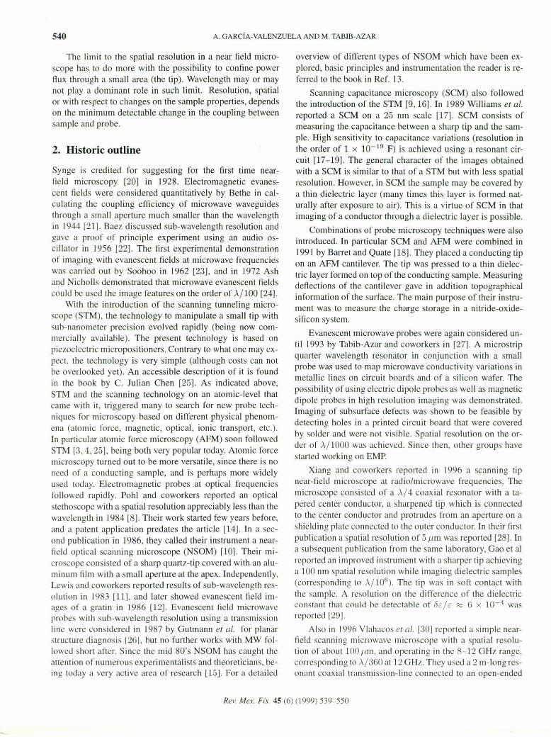
FIGURE 2. Side and bottorn views of a possible tip geometry.
-..• - Inner conductor
Coa'l.ialline
ConductingRing
OUler conductor
•
(a)
~.-
R, !.,Z.. .•.. -
I~'
lipwnple-........... ,,/-----.----~
3. Basic ruodel of a EMP
;l.i4Iransmi.sionlille scgmenl __ .•
FIGURE l. a) Schcrnatic layout of an EMP. b) Equivalent circuit ofthe >../4 resonator near rcsonance.
circulalor _.
The EMP consists ol' a short opcn-cndeo transmission-Iinewhieh eouples to the sample through a sharp lip (see Figs. Iand 2). The effeetive length, e, of the transmission line shouldhe close to >./4. It is not diffieult 10 show thal a quarler-wavelength transmission ¡¡ne is equivalent to a series reso-nant circuit [45]. The equivalent circuit analysis is used byseveral authors in previous works to model the probc sensitiv-ity [30,40,41]. In what follows we summarize lhe eleelriealaspects of the probe.The magnitudc of the reflection coeffi-cicnt'of a voltage wave impinging anta the rcsonator, ¡SIl 1,is mcasured, using for example a circulator and a squarc lawdetector [41J, as illustrated in Fig. la. The simplest method toimagc a samplc with a EMP is to keep a constant frequencyIx, and tip-samplc distance dI, and measure the resonator'srelleelion coeffieient, ISul as the prohe is seanned aeross lhesample's surfaee. Other possihililies are lo keep ISul and d,constant using a feedhack circuilry and measuring Ix, and. kceping 15111 and Ix constant and measuring dI. We willconsidcr only the first case, since it is the simplest. Dil'fer-ent kinds of transmission Hnes are possible.
coaxial prohe. No tapering of lhe inner conductor nor shield-ing pInte was used. In a second publication by lhe samegroup [31], Sleinhauer et al monitored Ihe frequeney shift oflhe resonance as (he open end of lhe transmission line wnsscanned c10scly lo Ihe samplc. using a frequency-followingc¡reuit. A sensitivity lo frequency shifts of 2 parts in 106 dUf-ing a 30 ms sampling time was achicvcd. They used theirEMP lo map surface resistance of rnetallie samplcs. Thcy es-timatcd a resolution in surface resistance of tlRx / Rx =0.05 for Rx = 100w/O.
The applieahility amI versatility ofEMP for their use withvery dinerent kind of material is illustraled by a series of re-eent papers from the group of M. Tabib-Azar [32-39J. Mi-crostrip or strip Hne rcsonalors wcrc used in lhe lancr works,illustrating thcir use with metal. semiconductors and insulu-tors, and wilh hiologieal and relevant medie al samples.
Quantitativc intcrprctations of lhe images require accu-rate rnodels of the tip and tip-samplc intcraction. Relativelyfew works have hecn dedicated so far to the theoreticalIllodels. Two recent papers give the foundations I"or suchwork [40, 41J. In ReL 40 Gao and Xiang proposed a quanli-tative theoretieal model l'or imaging die lec trie samples. Thcymodeled the [ip as a conducting sphere. They consideredin particular the case of imaging dielectrics (with real andcomplex dieleelrie eonstant). They allow a soft eonlael ofthe tip and sample, which enhance spatial resolution. Com-parison with cxperiment showed to be in good agrecment.They showed that the spatial resolution can be two orders01' magnitude less than lhe radius of the sphere (tip) whenE > 50 Eo. Their estimations indieate that nano meter spa-tial resolution is achievablc (lOO nm spatial resolution hasheen achieved already for E > 20 Eo [19]). Sueh a resolutionwould he comparable with that of NSOMs, but using a wavc-length lO" times larger. Thc resolutions to changcs in the di-electric constant is estimated in the order 01"ÓE/E ~ 10-5
for sueh a prohe. Tahib Azar el al., presenls a detailed anal-ysis of the scnsitivity of the resonator to perturbations dueto tip-sample interaetion [41]. Simple formulas for the reso-Jution, spatial and on changes in conductivity and dielectricconstant, arc given. The possibility 01"100 nm spatial reso-lutions using the microstrip rcsonator are predicted. Resolu-tions 01'óa/a ~ 10-2 in metal s, óa/a ~ 10-4 in semi-conduetors, and of JE/E '" 10-3 in dieleetries is predietedror 5uch a probe. An approach to enhance the spatial resolu-tion hy dcconvolving the EMP ¡mage with the cxperimcntallyII1casurcd spatial impulse response is investigated in Ref 42.
Finally, ncw analytical 100ls are being investigated byGarcía- Valen zuela el al. to calculate the capacitance betwcenelectrodes with arhilrarily rough surfaees [43,44]. The ap-proach is hascu on pcrturbative solutions to the boundary in-tegral cquation. Extensions ol' the rcsults to model the cou.pling capacitancc hctween a tip and a rough surface are still tohe done. Nevertheless, to dale it appears thal this is the mostattractivc approach to obtain analytical lI10dels for interpre-tation oí' vcry high resolution two-dimensional topographicalimagcs.
Rev. Mex. Fís. 45 (6) (1999) 539-550

542 A. GARCíA-VALENZUELA AND M. TABIB-AZAR
3.1. Analysis uf the resonator
Thc rctlcction cocfficient of lhe rcsonator is givcn by
Sll=Z;n-Zof, (1)Zin + ZOj
whcrc Zin is lhe input impedancc of lhe resonator and Z01 islhe characterislic impedance of lhe feed line. Using stantardtransmissioll line theory, Zin is given by
where Z,(» Zo) is lhe load impedance. For ciarily in lhe 1"01-lowing equations lel us define the complex perlurbing lerm,g(w) = g,(w) + jg;(w) = -2Zo/Z,. Assuming very lowlosses in lhe resonalor, and a frequency w close to lhe res-onance frequency of the unperturbed resonalor wo, we getusing (2),
Zin = Ro + 2jD.wLo -1Z09(w), (6)
(7)
(9h)
L' ,Q' = oWo
R'o
R~ = Ro -1Zogr(w),
L' =L -~Z (d9;) Io o 4 o dw ,,:,.'o
ami
where
3.2. Prohe-sample coupling
DilTerenl !ip geomelries have heen used, depending on lhekind ol' transmission line used for lhe resonator (microstrip,coaxial, cte.). In essence, £111 tips will work under the samchasic principies. From a conceplual point 01' view it is con-vcnienl lo consider Ihe OIlC depiclcd in Fig. 2. This is similar(o Ihe one used hy Xiang el al. in lhcir microscope [28,29].The outer conductor is extended towards the center conduc-tor wirh anal conducling ringo The inner conductor oC lhelransmission ¡¡ne exlenus heyond the ring through its aper-ture using a Ihin wire. Thc diamcter 01' sllch wire al ilS endwill determine Ihe prohc's spatial resolulion. As long as thewavelength in air 01'rhe microwaves is much smaller than Ihcring's diamcler and 01' Ihe distance betwccn lhe tip and lhering, we may use Ihc qll<Isistalic ¡¡mil.
The t1eld lines leave the inner conduclor's lip towards thering and olllcr COIHJUCtor.In {he presence 01'a sample, sornclicld li!les cnter the sample jusI helow lhe lip and exil below
Z'" = R~ + 2j L~D.w' = JI;, (1 + 2jQ' ~~'), (9'1)
l'mm where we salve for (¡.}h. The inductance and rcsistance oflhe pCrlurhcd resonator is found from rewriting Zin in terms01" D.w' = w - wb. Using g;(w) ~ g;(wb) + (dg;fdw)lw;D.w', 2jLoD.w = 2jLo(D.w' +wb - wo) we gel I"romahove,
which we may rewrite as
where we kept terms of ¡¡rst order in smallness only. The newresonance frequency (wb) is where Ihe imaginary componentin (6) is zero. Using ~w = w - wo, we gel
(5)
(2)
(4)
r = Z, - Zo 2ZoZ, + Zo '" 1 - Z, '
Zin = Ro + 2jD.wLo. (3)
Thc faclors t in lhe relati~ms R{J = !n£ anJ Lo !Leare Juc lo sinusoidal dependen ce of lhe voltage anJ currenlacross lhe resonalor. NOle Ihal at resonance the impedance isreal and smalIesl, lhe admittance is largest.
The circuit cquivalcnt 01' the lransmission ¡¡ne resonalor01' an EMP near rcsonance is shown in Fig. 1b. The reso-nance frequency of Ihe cquivalent circuit is 1/ J LeCe, whichis cqual lo Wo given ahovc, providcd Le = Lo = ~eL, andCe = SfC /'rr2, where C is Ihe capacilance pcr unit length01"Ihe resonator. The Q-factor is deflned considering the JJ-mitlance Yin = ljZin, which is maximum al resonancc.1l isdcllned as the 1'ractional oandwidth betwcen the poinls where)Yinl is 0.707 ol' ils maximum value. Prom (3) wc may l¡ndQ = LoiJ..,'o/ Ro, anJ wc may write
Z;" = Ro (1 + 2jQ ~~) .
If lhe prohe approaches the sample, coupling to the samplewill dc\'iale lhe rcllcction coefficienl r form unity. An EMPshould operatc under weak coupling lo the sample. Thus wemay approximalc
1 + rexp(-2')C)Zi" = Zo 1 _ r exp (- 2')0 '
whcrc Zo ::::J L/e is lhe characteristic impcdance 01' lhercsonator line, r is Ihe refiection cocfficient al lhe tip-end oflhe resonator, and f ::::o:+ jj:J, whcrc j is lhe imaginary unit.ror a low loss line a = 1RJC / L and (3 = wJCL, wherew is lhe radial frcqucncy, R, e, and L. are lhe rcsistance, C3-
pacitancc, ami inductancc per unit length of lhe resonalor'sline. respeclivcly.
Ir there is no tip-samplc coupling, lhe reflcction coeffi-cienl al lhe end of lhe probe is r = 1 (assuming Ihe open-circllited end). In lhis case, resonance (w = wo), is de-lined hy exp (2j(3£) = -1, ¡.e., (3C = 7f /2. Thus. wo =7f /(2C.;rc). 11"a is zero (a loss-Iess line), so is lhe inpulimpedancc, and thc admittance is infintc. Assuming very lowlosses (20(' « 1), and a frequency w c10se lo resonance:(3(wo + D.w).;rc = "Ir/2C+ D.w.;rc; wilh D.w.;rc «1/)., we gel I"rom (2), Zin = Zo(aC + jD.wLC), where wekepl terms of tirst ordcr in smallness. The resistance andinductance of lhe resonator are defined as Rn ~Re andLo = t Le, lhus we may write
Re!'. Me>x. J.b-. 45 (6) (1999) 539-550
EVANESCENT MICROWAVE PROBES AND MICROSCOPY 543
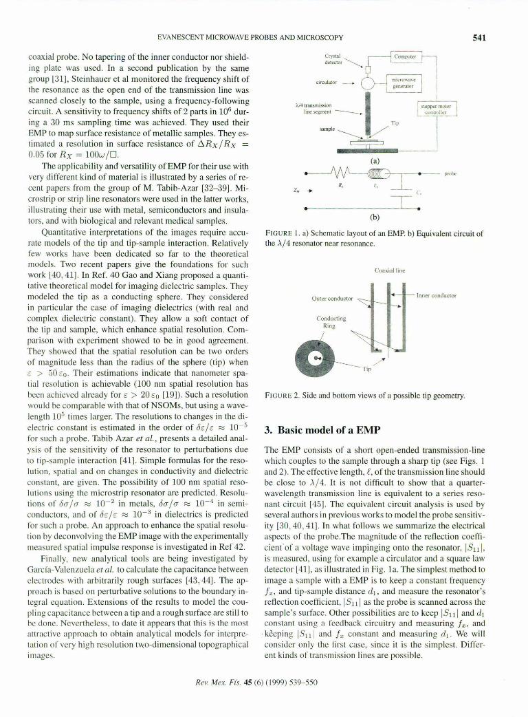
R .~~J'--, U.4"
FIGURE --l.Equivalenl circuil for the sample.~.~~ib
Srunr1c
--.. [J, ._
J
FIGURE 3. Schematic illustralion oC lhe eieclric field Hnes al lhelip-sample region. The lood impedonee Z, rnoy he eolculoted as Z, = 1'1/l. Us-
ing 1 = jWiiuE'I/fo we get from (11),
where the coupling capacilance is Ce = (CII + C:¡l )-1,
where CI = foJ"L,/dl• and C2 = foA'l/t1'l. lhe sample ea-
pacitance is Cs = fs.4o/delf, and the samplc's resistance is
R.~ = ddr/a.4n. Thc cquivalent circuit is shown in Fig. 4.Ir the s<lmplc is a nOllconl1uclive lossy dielectric. i.e., the di-eleetric constant is complex, fs = f~ - jf~, a is replaced (or
augrnenled) hy Wf~. i.e., Rs = defff~1 wf~Aa. In the caseof a good conductor we rnay need 10 inelude an inductive el-ernenl in series with the samplc's resistance due lo lhe timevarying magnetic field inducetl by the currents on the sam-pie. For simplicily we will not consider this term (see, e.g.ReL 36).
Using (12) in y(w) = -2Zo/Z, onu dcfining lhe smnpleconductance.fJs = 1/ Rs• we ohtain
lhe ring cnding on iI. Few of thcse ¡¡nes are illustratctlsehcmatically in Fig. 3. Let us assumc the tip antl ring aspcrfcel contluctors. Considcr one of the mentioned field Hnessuch as the dashcd field line in Fig. 3. At any instant of timc.the voltage difference between lhe tip and ring is given hyminus the inlegral of the electric ficld from point a lo f. Ifdi ami d'l in Fig, 3 are small compared with the diametcrnf Ihe tip onu ring respeelively, lhe eleelrie field moy he ap-proximated as constant within the gaps. (Thus. Ea = Eb andEc = El)' Much in the same way as in a parallel capacilorwhen ignoring fringing fielus. The field olong lhe line joiningpoinls e 10 d in the figure will he uepenuenl on lhe somple'seleetrieal properties and will vary along the length on the line.It will he largest at point e and smallesl at point d. We maywrite lhe corresponding integral as an effcctivc length limeslhe f¡eld 01 poinl e: Eedcff. Thus, lhe vo1Ioge differenee al lhelip is writtcn as
(10)
1 IZ, = -'--C + . C /R'Jf.J.,' e ]W 5 + 1 11
(12)
nnd
where Ca is lhe capacitancc uf the resunator, Ca = !CI, and
( 14)
(15)
( 13)
, ( ICe )Wo=wo 1-2Co
o:o,
y; +w'C,(Ce + C,)(\=----~--~y; + w'(C, + C,)'
id +W&C,(C, + C,)(tu = ,q; +W&(Ce + C,)' ,
whcre
with,q, = I/R,.
To a first approximation we may replace Q hy no == Q
(w = wo) in (12). Thus (dy;fdw)lwo = -2ZoCeQo. Usinglhis result in (S). we ohtain lo a first approximation,
Thc current density at point e is .T = a Ee, where a is Iheconductivity of lhe sample. The total current may be writ.
(cn as 1 = 17Ec.4c• where ,.le is an effective arca al pointr, which eommonly will he elose to the actual arca of thecross seelion of the tipo On the other hand, the current dCIl-sily may he expressed in terms of the current fluw I"rom Ihe
inlerfacc: .f = 17Ee = -óp/6t = - jwpc. fram where we gCI{le = aEe/ jw (j is Ihe imaginary unir). Applying Gauss' law
on the interface hetween point b and e in the figure, we get
E,E,. - ooE. = (JE,fjw. Thus, E, = EoE./(o, + (J/jw).Thc licld's amplilude within the gaps may be written in tennsnI' the effeetive ore of the ring (,.i ¡) ond tip ("Ia), ond lhe
averagc surfacc charge on thcm: En = Eb = (Ju/fo andEl = El' = PI/fa. The tOlal current 1 musl be expressed in
Icnns of;'1I1 cffective arca, as 1 = jwpaAa = jWfOftl En, or
as 1 = JWEoA¡E¡. Using hoth equations yields E¡ = Ee =E1•.l.¡,.1I. Bence, the voltagc is
Re\'. Mex. Fr,. 45 (6) (1999) 539-550
A. GARCÍA-VALENZUELA ANO M. 'IABIB-AZAR
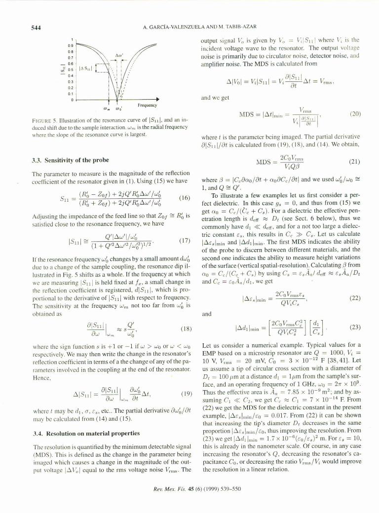
FIGURE 5. IIIUSlration of the resonance curve of ISIlI, anu an in-duceu shifl due lo the s3mple interaclion. wm is lhe radial frequencywhere (he ~lope of lhe resonance curve is largest. where t is lhe parameter being imagcd. The parlial derivalive
015111/ DI is ealculateJ from ( 19). ( 18). and ( 14), We ohtain,
(20),lOS If!. 1 \'rms~' = t mill = \' I iJlSllll'1 a,
anJ \Ve geL
'1\'1_ 1"15 1- \!,OISIII, - \'.:.J. o - l 11 - l----¡=]fut - UIIS'
OUlput ~ignal \/~ is given hy \.~, = \ "¡15IlI wherc \"/ is lheilh.:idenl voltage wave to lhe rcsonator. Thc Ollt(lllt voltageIloisc is primarily due to circulalor noise, de lector noisc. andamplifier noise. The MOS is ealculated from
Frequency
ó(v'
"o.,"07
_ 06
~ 05- 041
03 •
"j"1o
where {3= ¡C,Dao/Dt + aoDC,/Dtl and we used w~/wo ~1, and Q ~ Q'.
To illustratc a few examplcs let us firsl consider a per-feet dielectrie. In this case 1/, = O, and thus from (15) weget "o = C,/(G', + C,). For a Jieleetrie the effcctive pen-etration length is n",fr ::::::DI (sce Sect. 6 below). Ihus wecommonly have dI « df'tr. and for a not too largc a dielec-trie eonstant E.~. Ihis results in Cc » Cs. Let us calculateIllE,lm;n and If!.ddm;n. The tirst MOS indieates the ability01' the probc to discern between different materials. and lhesecond one indicaLes lhe ability 10 measure height variations01'the surfaee (vertical spatial-resolution). Calculating {3from"o = C,/(C, + C,) hy using C.• = ¿.•A"I d.ff '" E,A,,/D,and Ce = Eo.4.f1/d1, \ ••..e get
.1.3. Sens;!;,.;l)' of lhe prohe
The parameter lo measure is the magnilude of lhe retlectioncocfficicnt of lhe resonalOr given in (1). Using (15) we have
(R~ - ZOf) + 2jQ' R~f!.w' /w~511 = (R~+Zof)+2jQ'R~f!.w'/w~ (16)
Adjusling the impedance of lhe feed ¡ine so that 201 E:!:R~issalisf1ed c10se lo lhe resonance frequency, we have
¡rthe resonancc frequcncy wb changes hy a small amounL dwbdue 10a changc of Lhesamplc coupling. lhe rcsonancc dip il-lustrated in Fig. 5 shifts as a whole. If the frequeney at whiehwe are measuring 15111 is held fixed al fr. a small change inIhe rel1ectioll coefficient is regislcrcd, rI15111. which is prn-porlional lO the derivative ol' 15111 with respect lo frcquel1cy.Thc sensitivity at Ihe frequency wlll not too far I"rom I.J..':J isohtaineo as and
:L\lDS = 2Co l'rms, \t,Q{3
1 I2Co VrmsE s
.ó...:.~ lIIin = CQl~.
(21 )
(22)
( 18) If!.l 1 . = [2Col~m,C¡] [~]( 1 mm QVC:l C'. , , (23)
""here the sign funclion s is +1m -1 ir w > u..'oor w' < (w'orespectively. We Illay then write the change in lhe resonator'srelleclion eoeflkienl in lerms 01"a the ehange of any 01'Ihe pa-rmnelers involved in the coupling at lhe end of the resonatm.Hellce.
( 19)
where I Ill<lYhe d¡, a. E.~, elc .. Thc partial derivalivc Dv.-':,/ DIm,,)' he ealeulateJ from (14) anJ (15),
JA. Resolution un material propcrties
The resolution is quantiflcd by lhe minimum detectable signal(MDS). This is delined as the change in lhe parameter beingi11lagedwhieh causes a ehange in Lhcmagnitude of the ouL-pUl vollagc I~\:,1equal 10 lhe rms vohage noise Vrllls' The
Lel us eonsiJer a numerieal example. Typical values fm aEMP based 011 a microstrip resonalor are Q = 1000, \I¡ =10 V. \1""., = 20 mV, Co = 3 X 10-12 F [38,41]. Letus assume a tip of circular CfüSS section wilh a diameter ofD, = 1001"11 at a distanee d, = l/lm from the sample's sur-face, and an operaling frequency of 1 GHz, r.o..o = 2rr x 109.Thus the elTcctivc arca is .4.(1= 7.85 x ID-9m2; and by as-suming el « C"!., we get Ce ::::::Cl = 7 X 10-11 F. From(22) wc get lhe MDS for the dieleClric constant in the presentexample, If!.t.,["ü,,/Eo = O.Olí. From (22) it can he shownthat incrcasing lhe tip's JiamClcr D, decrcases in lhe sameproportion 1~E".~lllIíll/Eo.Ihus improving lhe resolution. From(23) we getllld¡I",¡" = l.í x 1O-0(Eo/t,)2 m. For E, = 10.this is already in the nanomcler seale. Of course. in any caseinercasing the rcsonator's Q. dccreasing lhe resonator's ca-pacitancc Co. ordecreasing the ralio VrlH~/\li wOllld improvethe resolulion in a linear rcialion,
Rel', Me.\". PÚ. 45 (6) (1999) 539-550

EVANESCENT M ICROWAV E PROIlES ANIJ MICROSCOPY 545Lel us considcr lhe sUllle probc values in an exal11-
pie wilh a semiconductor. Thc minimum detectable changcin lhe coupling resislancc Rs is found following lheahove proeedure as I""R,imón = [(2Co\l"n,) /(Q\1;)][(1 +., "/ :l:l ., 3] . / - ..'R.;wr¡Cc) /2R.'1wóCe . USlng R.o¡ = ".'1rit'lr ...1(1, wherc ,.,'1 IS
Ihe rcsislivity, wc gel
l~r...llllill :::::
(24)
where we used d,lf '" DI « J (see See\. 6 helow). As aIllllllcrical cxamplc, wc ohtain from (24) ror lhe prcscnt cx-i1mplc D..7'.'1lmin/l's = 2.7 x 10-2,4,7 X 10-4, 2,D x 10-:1,1l.3, and 28, for,., = 10-2, 10-1, 1, 10, and 102 flm, re-spcctiycly. Note 1hat I.ó.rslmin is a complicatcd function 01'w'u, Dio rll, and ,.,. Thus, hy using (24) one should ehooselhe lip's diamctcr and distancc (o maximizc resolution ror lhecxpcclcd rangc 01' resistivity. Sincc our model docs nol ¡n-elude an inductive lcrm in the coupling impcdance, we cannot extcntl our calculalions to gooo conductors. such as mel-als. This casc is considered in Ref. 41. Following a similarprocedure. and assuming a resistivity 01' f's ~ 0.1 !lm, weohlaincd l.6.tl11lllin = 2 X 10⁻¹⁰ lTl for the presenl cxample.This is a quile impressive resolulion, comparable lo what one(.;•.1Il get with aplical techniqucs in practice.
Nole that when imaging a perfect diclectric [formulas(22) and (23)], the only dependenee on A is due lo lhe fre-lJuency dcpcndcnce of Cf;ó due to the dispersion characteris-t¡cs of the dielectric constant Es. In the case of a semiconduc-tor, there is some additional depcndence on lhe frequcncy.according to (24).
4. DilTerences wilh other electromagneticprohes
As mcntioncd aboye, EMP may he rcgarded as rclated((l NSOM and to SCM. Howcvcr, direct rclalion betwecnNSOM and SCM is nol ohvious, if any. In lhis sense, an EMPlIlay he considered as "in helween" SCM and NSOM. Wediscllss in this section the main differences and advantages 01'EMPs wilh respeet 10 SCM and NSOM.
At microwave (MW) frequencies very good conduclOrsexisl, while al visible and near infrarcd frequencies real met-als are fairly poor conductors. Hencc, at MW frequencicslow-Ioss Iransmission ¡ines are a practical realization. Trnns-mission lines propagate TEM waves which have no cul-off frcquency. The electromagnctic ficld is confined withinllletallic conduclors and allows to concentrate the powcr fluxaeross <111arca wilh linear dimensions much smaller than thew<lvelenglh.
Atlcmpts lo implement and use lransmission ¡ines at op-lieal frequencies for NSOM have not been successful [131.
In the optical regime, dicieclrie wH\'cguides are uscd. Diclce-trie wavcguides, wilh few exceptions, propagate TE and Tl\'1ll10des only, all of whieh ha ve H cutoff frequency. For a thinwavcgllidc wilh dimcnsions sll1allcr Ihan a waveleng[h thesemodes are not presenl. In slep-index wavcguides with circulareross scetioll, Ihe fundamental hyhrid mode EMu, is one ofIhe exccptiolls, ami has no elllolT [4GJ. In NSOM the tip mayhe formed hy lapering the end of a aptical fiber. At the tip, theeore has disappeared and the cladding 01' the fiber bccomes[he eore. Forming a step index tiber: c1adding-air. At the tipIhe only guidcd mode is lhe fundamental mode. Howcver,Ihe lateral profile 01' the energy densily in the optieal lield01' Ihe EM¡¡ Illode remains in the order al' [he wavelength,even though, Ihe dimensions nf Ihe core may be small COI11-pared to the wavclcngth. Thus, power cannot be confincd lodimcnsions Illuch smaller Ihan Ihe wavclength and resolulionis not mlleh smaller lhan the wavclength. On Ihe other handcoupling efficiencies to the tip is in lhe arder of 10-6 113}.Olher possihility is to cover the lapcrcd region 01' the opti-cal guille with a melallayer. The fundamental mode becomesthen the TEll. This molle. though. eutotfs al a normalizcd(with respeet lo A) eore radius 01' 0.2. It deeays exponen-lially for smaller eore radius. For common taper angles thepower 105s lo lhe apex would render the tip uselcss. An opri-mal metal-coaled tir would taper gradually to cutol"" whereit would cnt! ahruplly. An apcrture in lhe metal coating on thehlunt end of l!lis tip would then provide further confinement01' the light anJ enhancc spalial-resolution. Thc aperturc di-amcter should be alm051 in the ordcr of the skin depth 01' thelight in Ihe metal. Olherwise Ihe aperturc would work as anover-dampcd wavcguidc resulting in furlher losses. The re-sulting Iimil on resolution for these probes is roughly 10 nmfor green light for lhe hest availahle metal (aluminum) 1131.Thus, the rcsolution is limiled due to the skin depth of lighlinto lhe metal. In eilher case, the power losscs on couplinglight i!llo a small arca with linear dimensions small eomparedlo the wavelenglh are vcry strong. Requiring [o work in thelower Iimil of the current pholon-deleelion lechnology. Thismakes NSOM expensive and requiring special careo
The ahove prohlems in NSOM are ahsent in EMP, he-ing this an important difference 01' EMP with regard to sub-wavelength imaging. As discussed in Sect. 3, the Iimil toIhe spalial resolulion in EMP comes from the unwanted cou-pling that may occur hetwcen the tip and the external con.duclor of Ihe transmission line, and 01' the rcsistance of thetip tllal comes wilh reducing ¡ts diameter. A 100 nm resolu-tion has been achieved, hut thcory prcdicts that smallcr res-olulions should he possihle in many cases [40]. ApparentlyEMP will achicve similar spatial resolutions than aperture-hased NSOM, although the wavelength is lypieaIly ¡¡ve or-Jcrs of magnitude largcr.
SCM using a UHF (ultrahigh frequency) resonant cir-euilI17-19] is also eloscly related lo EMP, in fael SCM maybe considered as a precursor of EMP. The cOllpling capaci-lance helween the lip and salllple plays a central role in cilherlechnique, and bOlh may use a resonant structure lo measure
Re •..Mex. Fú. 45 (6) (1999) 539-550
546 A GARCiA-VALENZUELA AND M TABII\-AZAR
lile coupling hetwccll sample and lip. The main differcllce he-Iweell lile two prohcs is Ihat capacilance microscopy uses a(on<.illcting suhstrate, which is gencrally grollnded lo the cas-ing 01"the resonant circuit. EMP, on Ihe other hand. can helIscd 10 ¡mage insulalOrs (with no conducling suhstralc). In'In El'\'lP the grountl is the external conductor in lhe Iransmis-sion tinc. which lIlay he tapered or extended hy a shieltlinglIletallic ring. EMP are also sensitive to Ihe surfacc rcsistancea",1 10 a cllective inJuctance [41]. In EMP the signal i, le"sensitivc to the hackground than in SCI\1. since the intlm:cdcurrents are conllnetl hclow Ihe tip. In SCM spalial rcsolu.lions in Ihe order of 25 nm have heen reporteJ lI7], "hile inEMP Ihe record resoiulion to date is 100 nm. In general welllay cxpect [hal comparahle resolutions should he achievetlw;tll hoth lechniqlles. As indicated, rcsollltions in Ihe few nmrangc are expcc(ctl 1'01'EMP (40).
5. Applicatiolls 01'EMP
The EMP signal depcnds on the c!ectric pcnnilivity E, mag-nc(ic penncahilily /', ami conductivity (1. 01' lhe sample aswcll as 011 lile topography 01' the surfacc. E, 11, and a. are ingeneral complex quantilies and tlepend on different physicalami chemical paramctcrs: Temperature, chemical composi-tion, 1110islure, stress. strain, density, etc. Thus, all the laterparameters may he imaged with an EMP for differcnt appli-c<lljons.
Many important physical etfects have temporal spe<.:trumsin (he microwave regime; e.g. rotation 01"small molc<.:ules,\lending Illotles 01' macromolecules, elc. Liquid water, heinga very important component of hiological systems. absorbsstrongly in the microwave regime. On Ihe other hand, thecOllductivity at t\.l\V frequendes is commonly c10se 10 theDC conductivily. lIlaking the EMP a potenlial1y very lIsefulllol1-destructive tool for the elcctronic industry.
EMP may he recognized as a non-contact and non-tlcslrllcli\'e tool for Ihe imaging of insulators, semiconduc-lor ..•., and metals. EMP compliments optical and electronil'llIicI"OscopCS in Ihe rangc of O.Ol/un to 1 cm. Ol1e attractivefcalure 01' EMP ror applications is that a minimum 01' samplcpn:paration is gcnerally needed. Thc distance hetween prohc¡¡mi tip may vary from a small fraclion of a micromeler to afcw hllmlrctls nI' micrornelers. or more. Thc spalial resolutionhcillg strongly dependanl on the tip-samplc separation (onceIIlis is ¡arger than the lip's diameler). In the case 01' sOl11e in-sulating samplcs with sl1100th surfaccs, physical conlacl be-lwecn the lir and sample can he lIsed to enhance resolution.
t\lany applicalions do not reqllire sllo.micron resollltions,OUIa largc imagcd arca. Lowcr spatial rcsolution permils lO
sean (he EMP prohe furthcr a\vay from the sample's surface.In these cascs E!\1P Illay offcr new unique possihilities. suchas suosurface imaging while allowing large surfacc rough-m'ss, imaging of slicky surfaces, ami high sensitivily to ma-terial paramclers. \Vith relatively large lip-sample scparalionsil is <lIso possihle 10 image very hol surfaces. Suhsurface
featmes in metal s can he imagcd tlue to the larger penetra.lion lengths of microwavcs compared to infrared antl opticalwaves. Sean rales 01' 0.1 mlll/S have heen achicvetl with thepossihility of incrcasing it hy a factor 01' 10 [321. Such seanrates are relativcly very fasl (e.N. compared wilh STM andAfM), a",1 yicld EMP suitahle 1m nn-line anJ quality con-trol applic¿llions.
As <.Illon-deslruclive tool, EMP has the advantage aver ul-(rasonic tcsting 01' insulators in lhat MW have relativcly highIransmissioTl cocflicicnts across solid-air boundaries. Also,ultrasountl ahsorption coeflkients are much higher Ihan M\Vin dielcclrics.
On Ihe Iimitations 01' EMP we may point out the facl Ihatthe signal depends on the material parameters, lip-sample dis-tance, and topography, making it ncccssary in some cases tocompliment an EMP with a indcpendcnt sensor to ueal withIhe tip-sample separalion. An oplical fiber sensor has bccnlIsctl rOl" Ihis purpose in Refs. 35 ano 37. Image inlerpretationis then 110talways Irivial and llIay rcquire delailed modelingof Ihe EMP signal and some assumplions on lhe sample. Ofeourse. similar Iimitations apply to other local prohe micro-scopes as well. In the following suhsections, we summarizerecent work on applicalions 01' EMP.
5.1. Dicll'ctrics
A two dimensionalmap 01' Ihe dielectric conslant of a sampleconsisting 01"¡hree diclectric laycrs. I 111mwidc cacho and withdielcctric constants of 11.8, 5.5, and 3.6 was givclI in [351.The minimum detectahle change in the diclcctric constantwas delermincd 10 he 1.7%. Images of a 2 x 3 mm'.! regionof a carbon composite \>,,'ercohlaincd in Ref. 34. Delaminatedregions are clcar in the imagc when compared to Ihe imageof an inlacl samplc. Imaging 01' the tlielectric constanl pro-lile with vcry lligh resolution (>=::: lOO 11m) of a Ihin dieleclric111mgrown in saphire slIbs(ralC hy dip coating was done inRef. 29. For sllch high resolulion the aulhors allowed softcontact (forre < 20 I,N) hClwcCIl lip antl samplc.
5.2. Semiconduclors
Dored silicoll wafers have heen used lo calibrate a EMP sig-nal as a function of resistivity 1351. Also varialion in resis-livity indllccd on a doped simiconuuctor upon shining lighlonlo il has bCCIl Illeasurcd with an EMP l341. A rcsistivityIllap over a .11/ 1.5/1111 3C-SiC on Si wafcr was obtaincd usingan EMP (llon-contacl mcasurclI1ent) in Ref. 34. Sincc lhe mi-crowave prohc rcsponse is quite fast « O.l/ls). the responsenf the scmiconductor lo an external stimulus, such as an opli-cal pulsc or depleling high-po\Ver eleclromagnelic pulse, canhe Illonilored. In lhe lale!" work. the response of a B-dopedsilicon samplc to pulses of light gencratcc! hy a GaAs laserdiode was lTlonitored lhrough lime using an Er-.lP. TransientIlleasurcmenls can he pcrformcd al ditlcrent lempcraturcs,ami since lhc microwavc prohc lIleasurcment is non~C()lltact,only the sample has lO be heated or coolcd. AClivation en-
Rel'. Ah'x. Fí.\". 45 (6) (1999) 539-550
EVANESCENT MICROWAVE PROBES AND MICI<OSCOPY 547crgics anu various paramclcrs uf deep levcls. such as thcircaplurc/cmission cross sccLions, and dcnsilics can he deter-rnincd. In lhe latel" cxpcrimcnt lhe carricr rccornhin<ltion ¡¡re-lime was cakulatcu fmm Ihe EMP signa!. Also lhe responseof a pholorcsislOr lOan optical pulse and Lhen lo hcating by a""'OmA pulse of currenl was monitored through lime wilh anEMP in ReL 36. These experiments shawed c1early the fea-sihility of using an EMP lo monitor variolls proccsscss thallllay takc place insidc a scmiconducting malcrials.
5.J. l\lelals
A M\V ¡mage 01' a printcd c¡rcuit board using 'ln EMP wasreponed in ReL 27. A previausly drilled hule cuvered withsolder was clearly visible in Ihe ¡mage; demonslrating Ihe C3-pahility o" suosurfacc Jefec! dctcction capahilitics 01'EMP.In ReL 33 il is shown thal an EMP can be operatcd in thelransmission mode to detect buried melallic lines in poorlyconducling materials. In Ref. 34 an EMP is used to image a2 mm diameter hole 00 a 6 mm thiek eopper piale. It wasfound that on doing a ¡¡oe sean across the hole, burrs al Iheedges can be detecled and charactcrized to sOllle degree. Inlhe S:lmc work it was shown thal an EMP can dClecl residualslress in melals based on Ihe capabilily 01'detectillg subsur-face conductivity ditTcrcnces. A scanoing imagc uf Iwo Nbstrips. 1000 Á thick, 10/1111wide, and 20 /"n apan was takenin ReL 28. The image 01'an array of squared eu f1lms Ihroughglass was also taken in Ihe later work. The dimcnsions were~OO/"n x 300 /1111and 1000 A thick in ane case, and 500/lInx 000 Iml and 2000 A lhick in olher case. The lip separationwas 200'lm.
Tlle use 01"an EMP lo image active microwave circuitswas suggested and demonstrated in Ref. 30. The EI\1P is con-verted lo a receiving mode and acts as a local microwavepickup. The image in a receiver mode of an excited mi-croslrip al 8.5 GHz \vas takcn. Tlle image shows c1ear mi-crowave standing wave excilalion on Ihe microstrip. Slein-hauer el al. (31jmeasured Ihe resonancc frequency 01' thcirEMP as a fllllCtioll 01'surfacc resistancc in Ihe range 58 n/olo 42 A"O/O . The s:lInple consisted 01'a variable-lhickncssthin-fiIm 01'oxidized aluminum on glass sublrale.
5.4. Hinlogical ~md mcdicnl applications
The 1II0islure-contenl nwp of a small region 01' a plant leaf\Vas oblained lIsing a EMP in Ref. 34. Some basic featuresuf lhe leaf. scen on an optical image. could be seen alsoon lhe MW imagc. In Ihe same work. higher moisture con-It:nl rcgions in halsa \\.'ood was also imaged c1early. Pol-ished specimens nf control and lrahecular bone of a humanfClIlurwere imagcd lIsing an EMP [32J. Por comparison thesamplcs were imaged using scanning acollslic microscopy(SAM). The iJllaging was done (in bOlh cases) lIlainlaininglile samples in a fluid cnvironmcnt. (delllonstr;'lling Ihe fea.sibilily 01' imaging lhrollgh a liquid with an EMP.) Resultssho\\' lhe possibilily of imaging al Ihe sallle time lhe c1aslic
and eleclrical properties of skelelal tissue al the micrometerlevel. In the salllc work the image ofthe cross seclion of a hu-man looth was ohtained. The aUlhors speculaled on lhe pos-sihility nf detecling incipienl caries wilhout ohvious cHnicalnor radiographic manifeslalion. Of course, EMP may be ap-plicd to olher hiological tissues. such as skin, cartilage. elc.In general. water and mineral content (such as Na+ and K+),heing imporlant biologieal constituenls can affeel the dielec-trie constan! antl condllclivity.
5.5. TCl11pcraturc \'ariations
Varialions in temperature 01'a resiSlive slrip cun be monitoredas a function of time in a point measuremenl using an EMP.The mechanislll is through varialions in the local conduclivilydue lo a change in tcmpcralure. Experimenlally a resolulionaf O.08°e was determined for the sample used in ReL 36.In Ihe same work. lransienl heating 01' a pholoresistor by a,40 mA pulse of cUITent was Illonitored using an EMP. Thercsults 01' this work indicale lhe capability of an EMP to dospatial ami lemporal therlllography.
5.6. Novel ph}'si<.'~lIand chemicnl sensors
In ReL 37 an EMP was uscd to monitor lhe resistivity of aPd film 011 a cantilever as a funclion 01"Hydrogcn concenlra-tion. The rcsistivity ch:lIlged by 13.5% al 3.0% concenlration01' H1 and il resulted in a change of 18% of the EMP sig-na!. Hydrogen concentralion in the range 0.01 % 104% couldhe detected. As lhe Pd film absorbs H2 it expands and Ihec'-lntilever beam dellects dowllwards. Such dcflection couldalso he detected hy the EMP. The EMI' with an apprapri-ale frequency can also be uscd lo resonanlly deleC! physi-absorbed Illolecules at the surfacc 01'lln appropriate materialas wel!. Thc performance of an EMP as a displacement sen-sor (displacemelll o" a canlilever) was addressed in dctail re-celllly [38J. Displacelllenl sensing in the range 0.01 11m lo:> cm is possihle.
Poinl sensors are of inlercsl because it could be possi-hle lo inlegrate a largc Illllllbcr of thelll into a reasonahlysil.ed sensor panel. Seleclivily and stability problems may hesolved lIsing signal processing of all sensor OUlputS.This, byIhe way is the solution naturc has chosen in hiological crca-tures. For poinl scnsors using EMP lOhe practical il would benceded to inlegrale lhe whole EMP inlo a single chip: EMPhave heell fahricalcd 011 high-resistivity silicon using sl<m-d"rd "¡in-olI" phutulitugraphy prócesses [~9J. The Q factors01"lhe rahricated rCSOII:llorswas very high (:::::13000). Thismay enahle inlegralioll of arrays 01' EI\1P and siJicon can-lilevcrs ror point chemical 01' physical sensors.
6. On lhe lransverse spatial resollltion
The Ir:lllSVerSeresolution ofthe pro be \ViIIclearly dcpend onIhe lip's diameler D,. Assuming Ihat lhe dislance lo Ihe sam-pIe ti is Illllch smallcr thJn D,. the fieltllines will he very in-
Rej'. M('x. Fú. 45 (6) (1l)l)<J) 539-550
A. GARCiA-VALENZUELA AND M TARIH-AZAR
1.2
D.12
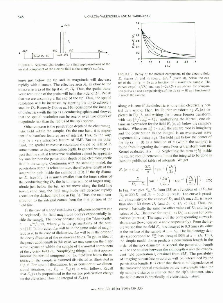
fll;URE 6. Assumcd distrihution (10 a first approx.imation) of lhenormal component 01'lhe clcctric f¡cld al lhe samplc's surfncc.
LÜ 0,8
? 06
"tU 0,4
02
oo 0.5 1.5 2
z ID,25 3
(~J]} (25)
tense just oelow lhe tir and its magnitudc will dccreascrapidly with distallcc. Thc elTective arca .4.0 is clase lO lhetrans\'crsc area 01' lhe tir ir di « DI. Thus, lhe spatial trans-vcrse rcsolution oflhe pro he will be in lhe order o" DI' RccallIhal wc are assuming anal cnd o •. lhe tipo Thus, lhe spatialrcsolution will be incrcascd by tapcring lhe (ir lo achicvc asmallcr Dt. Rcccntly Gao el al. [40] considcrcd Ihe imaging01"diclcctrics wilh lhe tir as a conducting sphcrc and showcdthat lhe spatial rcsolution can be one or cvcn 1wo ordcrs 01'magnilUdc Icss than Lhe radius 01' lhe tip's spherc.
Othcr conccrn is the penetration depth 01' the elcctromag-IIctic flcld wilhin Ihc salllplc. On the one hand it is impor-tanl ir slIhsurfacc featurcs are of interest. This. hy the way,tIlay he a vcry atlractive "eature 01' EMP. Bul 011 lhe otherhand. lile spalial tr.:tnsversc-rcsolution should he relalel! in"i(lIllCmanner lo lile penelralion depth. In general we may ex-pect that the spatial transvcrse resolution cannot he apprecia-hl)' smallcr than lhe penetration dcpth o" thc elcctromagneticlicld in the sample. Continuing wilh lhe same lip model. thepCllelratiol1 deplh is relatcd to deff. the cffectivc length 01' theinle~r"tion path inside Ihe sample in (10). II the lip di ame-ler D, (see Fig. 3) is much smaller than the inner radius 01'lhe cOIH.1ucting ring Di. the lleld Hnes will he 01' largest mag-nilude just helow the tipo As we move along lhe f1cld Hnetowards lhe ring. lhe lIcld magnitude will decreasc rapidly(consider Ihe dashed lielJ line in Fig. 3). Thus, thc l1lain con-Irihlltion 10 the integral comes fmm the firsl portion of the
lil'ld Iinc.Inthe t:ase of a good t:onJuclor (displacelllenl current can
he neg!ct:ted), the ticld l1lagnitude decays exponclllially in-side Ihe sample. Thc decay constant being lhc "skin-deplh",¡) = J'2/"';J/a. where JI is Ihe permeahilily 01' the sal1l-p1l.:[.1.11.In this case. IIt'lI" will he in the sal1le orJer of magni-lude as 6. Inlhe case 01' diclcctrics, detf will he in Ihe ordcr uflile deca)' dislance of lhe evanescent fielJs. To gel un iJea oí"lile penelralion length in Ihis case. \Vc may consider Ihe planewave expansion wilhin lhe sample of the nOI"malcomponentorille eleClric licld E
Il• Simplifying things, lo a lirst approx-
illlation lhe nOl"lIli.l1componenl 01' the ficld just hclow Ihe in~IL'rfacc 01' the samplc is assumeJ distrihuled as illuslraled inFig. 6. For case of illllslration. let liS consider a two dimen-sional silUalion, i.e.. £11 = En(.r) in what follows. Recalllhal £" (.r) is proportionallo the surl'ace polarizalion chargeon lhe dieleclric. Thus the integral of En(;r)
FIGURE 7. Dccay of Ihe normal componenl of Ihe electric field,E .• (l'urvc h), aml irs squarc. IE"I:.! (curve d). hclow the cen-ter of lhe tip (.1: = O) as a fUllclion 01" :; insidc the sample. Thecurves ('xp ( -: / D,) ami ('xp ( - 2.: / Di) are shown ror compan-son (l'urves a ano c rcspeclivcly).of the tip (.r = O) as a function of.: insidc lhe samplc.
along.r is I.cm if the Jielet:tric is to remain elcclrically neu-Iral as a whole. Thcn, hy Fourier lransforming En(:!.:) Jc-pit:ted in Pig. 6. anJ \Vriting thc invcrsc Fouricr transform.wi¡h "XI' [jVE.,kij - k:;z J I\lultiplyin~ ¡he Kernel, one ob-tains an express ion for the lielJ En(;r . .::::),belo\\' the samplc'ssurfat:c. \Vhenever k; > E .••k~ Ihc square rool is imaginaryallll lhe contrihulion lo lhe inlegral is an evanescent wave(exponcntially decaying). The lield JUSI helow lhe cenler oflhe lip (.1' = O) as a fUllclion of .::::(wilhin the sample) isfound fmm integrating lhe invcrse Fourier lransl'orm wilh theKernel cvalualcJ al ;17 = U. Neglecting the term £;k6 insideIhe squarc rool (clectmstalic Jimil) the integral to be done isfound in puhlished tahles of integrals. \Ve get
2E, { 1 (DI)E,,(.I = 0, z) = -- t"lI- -7í 2.::
___ D,_. [tllll-I (~~)) - tan-IDo D, --
In Pig. 7 wc plOl E,J E(' from (25) as a function 01"=/Dt forDo == '200 D, and Di = :)0 D, (curve h). The curve is pracli-cally insensitive 10 rhe vall1cs 01'Do ami Di once Do is largerlhan ¡¡hout :)0 times DI (alld Dt < Di < Do). Thus, thecurve is h:lsically the same for other values ol' Di illld largervalucs of Do. The curve rOl"('XP (-:; / DI) is shown for COI11-parison (curve a). Thc squarc of lhe corresponding curves isalso shown (Io\Ver curves, ti and (' respeclivcly). From lhe fig-ure we see lhat Ihe ¡¡e Id E,¡ has JccayeJ lo 0.3 timcs ilS valueat Ihe surface of the sample al .:: = Dt. The lield energy Jen-sily (proportional to E~) has decayed 90% at.:::: = DI. Thus.lhe simple moJel ahovc prcdicts a penclration Icngth in Iheorller of lile lip's diameIer. In ~~neral, Ihe pcnetration lengthwill hc lhe smaller hel\VCCll lhc skin dcplh r5' ami the cvanes-l'cnt ¡¡cid pelletratioll ~ ohlaincd rmm (25). The possihility01" imaging suhsurfacc slructures \Viii he determincd hy Ihepenetration lenglh. It is clcal" thal Ihere is no dependence ol'Ihe Iransverse spalial resolulion on the \\.avclcngth whcn Ihetip.samplc distancc is smal1cr than the lip's diinlletcr. sinceIhe lield pattern is praclically 01"eleclrostatic nalure.
Re". Me.r. Ft\.. 45 (6) (llJl)l)) 5JlJ-550

EVANESCENT MICROWAV E PROBES AND MICROSCOI'Y 5~9
lhere will be limilalions 10reducing D, for different rea-sonso On Ihe (lne hano. rcducing lhe diamcler of Ihe lir in-crcasc Ihe resislivily of the lir ilself. On lhe other hand, rc-ducing Ihe aperlure's dial1leler on the shielding ring (Di).lllay rcsult in unwanled coupling helwecn Ihe inncr amI outerconduclors forming the Iransmission lineo 80th effecls wouldIcnt! to reduce Ihe Q of Ihe rcsollalor and thus the sensitiv-ity and resolulion. Ol' course. the tip geometry ano the tip-sample inlcraclion should he aodressed in more detail anuIllOfe laborious models should he studied in the future lo an-swer qU<lntitatively the fundamcnlal questions on the EMPalllllhe quantitative inlerpretation of Ihe imaging.
6.1. Enhancing resolution
h././. SJllcrrmous derecrio"
The signal in a EtvlP is alTeeted by low frecuency noises\l,i'hichtend lo be larger. An interesting possihility for a moresophisticated detcclion schel11e is lo vibrate the sample (or(he lir) al a lixed frequcncy. The lip-sample distance beingthen an hannonic function of lime. The resulting AC signalhas :In <Implilude proportional lo the flrst derivalive of Ihel.:oupling capacitance \vith respecl lo Ihe tip-sample distance.This tirst derivative is a stronger function of distancc Ihan thecapacilance. On the olher hanJ the signal's amplilude can hemeasureo synchronously using a lock-in amplifler reducingL'onsiderahly Ihe effecl of random electrical noise, which is(he dominant noise in EMP. This detection scheme has al-ready heen uscd showing an improvemcnl in resolution [33 l.
{J./.2. D('("(mvoillfiol1 aigorithm
A simple dcconvolution melhod was dcveloped in Re!".42ami used lO sharpen the images laken with an EMP. The de-L'OIl\"oIUlionof EMP images improvcd Ihe spalial resolulionhy al Icasl a factor of 2 in cases in which lhe inherent spa-tial resolution was very high (O.4¡lIn) and by a factor of .1whcll lhe resolulion was low (otO ¡un). The method is hascdun llleasuring the spatial impulse response (or roint spreadfunclion) of the prohe. Assuming Ihat. lo a gooo approxima-(ion, (hc EMP image is the convolution of the experimenlal:-.patial-implllse response. this function is used to deconvolvelhc imagc. Thesc results givc moti val ion to improve Ihe cur-rcnl Illooels of the tip-sumple inlcraclion and lip designo
()./.3. ;\//{/iyticnilOo/s
NUlllcrical schcmcs (such as linitc difference methol!s) areuscflll lools in modcling the lip sample coupling. HO\\.'cvcr,\\/hen dcaling with two-dimensional problems, nUlllerical cal-l.:ulatiollS rcquirc e.\ccssivc eompulcr memor)'. Additiollally.1l1l111Cricalschemes do not provide Illuch physical insighl intolhe prohlcJ11.Analytical approximate rcsulls can he vcry usc-fuI when dealillg with real two-l!imensional structures ami
can providc hettcr accuracy w¡th much less crrort. Furlher-more, analytical results may provide. in somc cases, inversealgorithms for image interprelation and spatial rcsolution cn-hancelllenl.
\Vhen accuralc lo model lhe tip as a conoucling sphereand the sample's surface as llat. simple analytical results canhe ohtained 1401. Howevcr. for vcry-high resolution. in whichdI « D" il may he more appropriate 10 moJel lhe sensingregiun of Ihe tir as a llal electrode with some protrusion actu-ally functioning as Ihe tip and a rough surfilce ol"the sample.In this case. few analytical lOols have heen de\'eloped. Re-cenlly the prohlem of a capacitor with a rough eleclrode hasheen addrcssed. Analylical results lhat lTlayallow to calculateaccurately Ihe capacitance have heen stuJicd hased on a per-turhalive solUlioll 10the houndary integral equalions [43], andcxtcnsions have heen sought using a simple approach sug-gested hy lhe Padé-approximation melhod [44]. Until now.only Gne eleclrode has heen considered rough. It is neccssary10.extcnd the \\'ork to (he case of two rough elcctrodes with aclcar prolrusioll working as lhe tip. Abo, il will be neccssaryto extend the work lo deal with olle rough electrooe. a roughdieleclric interfacc and anal electrodc. Thcse cXlensions arcin principlc possihle and should bc studied in the future.
7. Summary and final commenl~
\Ve prcsenled an overview 01"lhe t1cvclopment and presenlstale of development 01"the Evanescent Microwave Prohesand their use in microscopic characlcrizalion oí" malerials.The EMP is a novel Ilon-destructive non-contact tool for thecharacteriratioll ()r sensing 01'insulalOrs, semiconductors anuIlletals. EMP can ohtain a Iwo-dimensional image of the mi-crowave propcrties of material s with very high.resolution.Images of the topography and suhsurfacc fealures can be oh-tained as wel!. The EMP complimenl other microscopy tcch-niques in lhe range 01"sub-micron to millimeter resolution.
Among Ihe prindral attractive fcatures uf these probcs istheir rclalive simplicity, the lack 01"time consuming samplepreparatioll, \vide range 01"spatial-resolution (suhmicron 10millimeter resolutions), fasl scan mtes. and high sensitivity 10eleclrical raramelcrs nf the samplc. Among the mosl attrac-live carahilities of these prohes are: Non-colltilct surface rc-sistance measurcmenl anJ imaging 01"colo and hot surfaces.novel hiological and Illedical applications. and suh-surfaceimaging of defecls in Illctals.
Thcorelical modeling of lhe tip-samplc interaction forIhe quantitative intcrpretation of images anu for improvingthe (ip designs l"nreach applicalion should be a hne of fUl"-ther rescarch. An cvalualion of the diffcrenl signal process-ing schel1lcs proposed to date should he abo of inlerest, asweH as proposing new tcchniques. No fundamental resolu-tion I¡mit has heen formulated to Jale. and !llore analysis inthis rcspcct is llccdcd. Spatial rcsolu(ion in (he fcw nanomclcrrange are expected to he possihle in many cases.
Et\1P may also he rcgarded as lhe core for a new c1ass ofsensors. Inlcgralioll of microwavc rcsonators with eleclronics
Re\'. Me.\. F¡".\'. 45 (6) (1999) 539-550

550 A. GARCíA.VALENZUELA ANO M. TABIB-AZAR
in a single chip is alrcady lInder invcstigation and may opena wide r~lI1gcof possihilitics in crcaling !lew sensors ano pan-els of SCIlSors fOI"chcmical ano hiological applications. Many
1. G. Billllill~ amI 11.Rohrer, He/v. Phys. Acta. 55 (1982) 726.
2. G. Ailllling. H. Rohrer. Ch. Gcrhcr. and E. WeibcJ, Apl'f. Pln'sIA'II. 411(l9X2) 17X, Php. R",. U'II. 50 (l9X3) 120.
:3. G. I3inning. c.F. Qualc, and Ch. Gcrbcr. Plt)'s. Rev. Lell. 56(19X61930
4. S. Akxandcr l'( a/.. 1. AI'I'I. Php', 65 (1989) 164.
G. Y. Martín ami Il.K. Wickwmasinghc, Apl'l. Phys. U'Il. 50(19X7) 1455.
G. CC Williallls and IIK. Wickralllasinghe, Proc. SPIE X97(IYXX) 129.
7. P.K. Hanslll~l('laJ., SciellCl' 24] (1989) 641.
8. D.W. Pohl. W, Dcnk. and M. Lanz. AI'I" Phys. Lett. 4-t (1984)651.
D. JR. Maley ano J. llIane, 1. Al'l'l. Phys. 47 (1985) 1437.
10. U. During. D.W. Pohl. and F. Rnhncr. 1. Al'l'f. Ph.vs. 59 (1986)JJ IX.
11. A. Lcwí~. 1\1. Isaacson. A. Murray. and A. Harootunian. 8io./,1.,'.> 1. 41 09X3) 405.
12. E. BCllig C'/ al..lli0l'hYJ. 1. .t9 (1986) 269.
1:J. 1\1.A. Pacslcr and P.J. Moyer, Nellr-Jield ol'tics: Tllenr)'. iJHtl"ll-
1/l(,lIfatioJl, amI 1l1'1,licatioflS, (John Wilcy & Sonso lne., NewYorlo-. 1996).
1.1. D. Puhl. Europcan patcn( application no. 0112401. Dee. 2719H2; US palcnt 4 604 520, Dec. 201983.
15. (Al1 artides in NO.I-4) Ullml1licroscopy71 (1998).
16. CD.llllggand I'.J. King.J. Phys. 1:21 (1988) 147.
17. ce. Williams. W,P. Ilough. ane!S.A. Rishton. Apl". Ph:rs. Len55 (19X9) 203.
18. R,e. Barret ami C.F Qualc. 1. AI'J'1. Phys. 70 (1991) 2725.
19. G. Ncubaucr ('lal., 1. \!tIC.Sci. T('clmo/. B 14 (1996) -1-26.
20. E.II. Synge. Pililos M(J~.6 (1928) 356.
21. II.A. Betlle. Phy.\'. R{,l~66 (1944) 163.
~2. A.V Bacz. 1. 0IJl. SOl'. Am. -1-(,(1956) 901.
~;3. R.F 5001100. 1. A/I/,I. PIlys. 33 (1982) 1276.
24. E.A. Asll and G. Nicholls. Natllre 237 (1972) 510.
2~. e. Julian Chen. Immduclioll to .{clIfllI;ng tll1l1U:Jitlgm;erm,copy.(Oxford Univcrsity Pre!">s.Ncw York. 1993).
!lew applicatiol1s 01"E~,tP are still awaiting lo be cxplorcd.As with Illost !leal" licld probcs, new technical ano thcoreticalisslIcs will arise wirh new applications.
26. R..J. GlItma:lIl. J.M. Borrego. P.C hakraharti. and Wang Ming-Shan, IEI,'1,' MIT.S /JiRe.H, (1987) 281.
'1.7. M. Tahih-Azar. N.S. Shocmaker. and S. Harris. Ml'as. Se;. Tech.f/o/. 4 (1993) 583.
28. T. \Vci. X.D. Xiang, \V.G. \Vallacc-Freedman, and P.G. Schultz,AI'pl. I'hys, Lel/. 6X (1996) 3506.
29. Che n Ciao ¡,( al., AI'II/. PIlys. Lell. 71 (1997) 1872,
JO. c.P. VlahaCOSl'lal .. A/1/11.Phys. Ll'tt. 69(1996) 3272.
31. D.E. Steinhaucr el al .• AI'I,I. Phys. Let(. 71 (1997) 1736.
32. M. Tahih-Alar, S. Bumrcrraj, J.L. Katz, and S.R. LcClair,(1999) (suhmittcd).
33. M. Tabih-Azar, R. Ciocnn. G. Ponchak. nnd S.R. LeClair,(1999) (!">uhmitred).
34. M. Tahih-Azar. P.S. Pathak. G. Ponchak, and S,R. LeClair, Re\'.Sci. blJtml1l. 711(1999) 2783.
35. M. Tahih-Azar el al.. R{'I'. Sci. 1m/rumo 70 (1999) 1725.
36. f\1. Tahih-Alar, R. Ciocan, G. Ponchak, and S.R. LcClair, Rel'.Sá./n.\'II"WIl. 7U (1999) in press.
37. t\1. -nlhib-Azar. Boonsong Sutapun. G. Ponchak, and S.R.LcClair. (1999) (suhmittcd).
.18. M. Tahih-Al.ar. Dcji Akinwandc, G. Ponchak. and S.R. LeClair,R(,!,. Sci. /II.1tntlll. 7n (199lJ) (in press).
39. M. T:lhih-Awr. D. Akillwandc, G. Ponchak, and S.R. LcClair,Un' .. )'ci. 111.1"(1"1I11I. 7U (1999) (in prcss).
-10. C. Gao ami X.D. Xiang, R{'\'. Se;. butrwn. 69 (1998) 3846.
11. M. Tahih-Azar. O,P. Su. S.R. LcClair. and G. Ponchad. (1999)(suhmiltcd).
,1:2. M. Tahih-A/ar. R Cioc<ln. S.I1. YOll. amI S.R. LcClair. (1999)(SUhlllillcd).
43. A. Gan.:ía. ValcllZllcb, Bruce C. Ncil. nnd D. Kouznctsov, 1.Phys. f), A/I/JI. Phys. 31 (1998) 240.
4.1. N.e. Brucc. A. Garda-ValclllUcla. and D. Kouznctsov, 1. Phys.IJ "1'/,1. Phy.\'. (1999) (suhmittcd).
.15 R.E. Collin. ¡:(l/I/ulat;o/l.\' o!"m;cmw{l\'(' l'flginc('Tillg, (t\-1cGraw-Hil!. Sing;,pore. ¡t)66).
-l.G. S, Ramo. J,R. Winnery. :llld T. Van Duzer. Fit'lds {l1/{1 Wm'CS;1I
COllllllltll;n/fIIJII {J/"{'{HI/I;n. (Wiley, New York, 199-1-).
R('I'. M".\". Fi.\. 45 (6) (199(») 539-550