Embed Size (px)
Citation preview

TitleEvaluation of the delamination in a flip chip using anisotropicconductive adhesive films under moisture/reflow sensitivitytest
Author(s) Ikeda, T; Kim, WK; Miyazaki, N
Citation IEEE TRANSACTIONS ON COMPONENTS ANDPACKAGING TECHNOLOGIES (2006), 29(3): 551-559
Issue Date 2006-09
URL http://hdl.handle.net/2433/39974
Right
(c)2006 IEEE. Personal use of this material is permitted.However, permission to reprint/republish this material foradvertising or promotional purposes or for creating newcollective works for resale or redistribution to servers or lists,or to reuse any copyrighted component of this work in otherworks must be obtained from the IEEE.
Type Journal Article
Textversion publisher
Kyoto University

IEEE TRANSACTIONS ON COMPONENTS AND PACKAGING TECHNOLOGIES, VOL. 29, NO. 3, SEPTEMBER 2006 551
Evaluation of the Delamination in a Flip Chip UsingAnisotropic Conductive Adhesive Films Under
Moisture/Reflow Sensitivity TestToru Ikeda, Won-Keun Kim, and Noriyuki Miyazaki
Abstract—Anisotropic conductive adhesive films (ACFs) havebeen used for electronic assemblies such as the connection betweena liquid crystal display panel and a flexible printed circuit board.ACF interconnection is expected to be a key technology for flipchip packaging, system-in-packaging, and chip size packaging.This paper presents a methodology for quantitative evaluation ofthe delamination in a flip chip interconnected by an ACF undermoisture/reflow sensitivity tests. Moisture concentration aftermoisture absorption was obtained by the finite element method.Then, the vapor pressure in the flip chip during solder reflowprocess was estimated. Finally the delamination was predicted bycomparing the stress intensity factor of an interface crack due tovapor pressure with the delamination toughness. It is found thatthe delamination is well predicted by the present methodology.
Index Terms—Anisotropic conductive adhesive films (ACFs), de-lamination toughness, flip chip, moisture/reflow sensitivity test, re-liability, stress intensity factor.
I. INTRODUCTION
AN anisotropic conductive adhesive film (ACF) is an adhe-sive containing conductive particles that supply electrical
interconnections. Most of the current products are thermosetplastics. The ACF has been used for electronic assemblies suchas the connection between a liquid crystal display (LCD) paneland a flexible printed circuit board (PCB) [1], [2]. Comparedwith traditional solder interconnection technology, the ACF in-terconnections have several advantages such as fine pitch, flex-ibility, low temperature processing, etc. The ACF interconnec-tion is expected to be a key technology for flip chip packaging,system-in-packaging, and chip size packaging (CSP) [3]–[8].
Flip chip packages interconnected by the ACF are often used,together with surface mount devices (SMDs). In such a case,solder interconnections are utilized for the SMDs, so the ACFsin the flip chip packages are subjected to temperatures ranging
Manuscript received October 10, 2004; revised November 11, 2005. Thiswork was supported in part by a Grant from the Foundation for Technology Pro-motion of Electronic Circuit Boards, and by a Grant from the Fukuoka Projectin the Cooperative Link of Unique Science and Technology for Economy Re-vitalization (CLUSTER) of the Ministry of Education, Culture, Sports, Scienceand Technology (MEXT) of Japan. This work was recommended for publica-tion by Associate Editor J. Morris upon evaluation of the reviewers’ comments.
T. Ikeda and N. Miyazaki are with the Department of Mechanical En-gineering and Science, Kyoto University, Kyoto 606-8501, Japan (e-mail:[email protected]).
W.-K. Kim is with Interconnect Product and Technology, Samsung Elec-tronics Co., Ltd., Seoul 100-742, Korea.
Color versions of Figs. 1, 2, 4, and 11–13 are available online at http://ieeex-plore.ieee.org.
Digital Object Identifier 10.1109/TCAPT.2006.880510
from 240 C to 245 C during the solder reflow process. In addi-tion to an increase in electric resistance, electric disconnectionis also sometimes observed in the flip chip packages using theACF interconnections during the solder reflow process [9], [10].Such phenomena are caused by the delamination initiated fromthe interface between a chip and the ACF or a substrate and theACF. It is therefore important to ensure the mechanical relia-bility of the ACF interconnections when they are used for flipchip packages instead of solder interconnections.
In the present paper, a methodology for evaluating thedelamination of the ACF interconnection is proposed. Manyresearchers have previously studied to predict crack occur-rence from a corner of jointed components in plastic packages[11]–[14]. In these studies, fracture mechanics were applied tothe failure of plastic packages. As in these studies, we appliedthe fracture mechanics for an interface crack to the delamina-tion of the ACF interconnection. The delamination tests areperformed on joints composed of the ACF and the constituentmaterials of a flip chip. Then the delamination strengths areevaluated using the stress intensity factors of an interfacecrack between jointed dissimilar materials. The moisture con-centration in the flip chip after a moisture absorption test isanalyzed by the finite element method, and the vapor pressurecaused by the solder reflow process was estimated. Finally thedelamination in the flip chip during the solder reflow processwas predicted by comparing the delamination strength with thestress intensity factors caused by vapor pressure.
II. ESTIMATION OF DELAMINATION STRENGTH
A. Delamination Tests
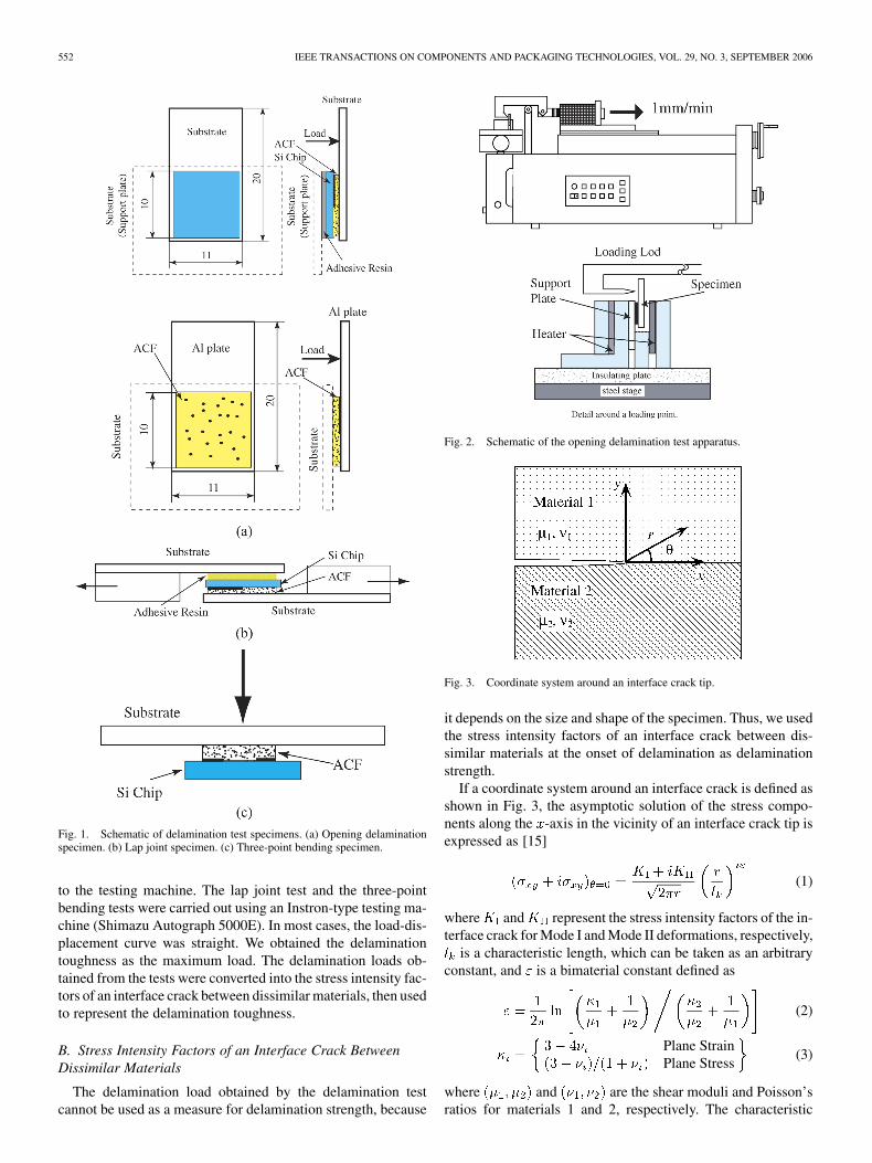
Delamination tests were performed on opening delaminationspecimens, lap joint specimens, and three-point bending spec-imens, as shown in Fig. 1. The initial delamination was intro-duced by a painting release agent on the surface of a siliconchip, on the surface of a substrate, or on the surface of an alu-minum plate. Since the silicon chip is very brittle, the chip wasreinforced by pasting a substrate (a lap joint specimen and athree-point bending specimen) or a support plate (an openingdelamination test specimen) using epoxy adhesive resin to pre-vent its failure due to bending force. Delamination tests wereperformed at five different temperatures, 25 C, 60 C, 95 C,120 C , and 240 C, and at the test speed of 1 mm/min. Theopening test was performed using a special apparatus as shownin Fig. 2. In this figure, the support plate has two roles, as a rein-forced plate and as the location where the specimen is attached
1521-3331/$20.00 © 2006 IEEE
552 IEEE TRANSACTIONS ON COMPONENTS AND PACKAGING TECHNOLOGIES, VOL. 29, NO. 3, SEPTEMBER 2006
Fig. 1. Schematic of delamination test specimens. (a) Opening delaminationspecimen. (b) Lap joint specimen. (c) Three-point bending specimen.
to the testing machine. The lap joint test and the three-pointbending tests were carried out using an Instron-type testing ma-chine (Shimazu Autograph 5000E). In most cases, the load-dis-placement curve was straight. We obtained the delaminationtoughness as the maximum load. The delamination loads ob-tained from the tests were converted into the stress intensity fac-tors of an interface crack between dissimilar materials, then usedto represent the delamination toughness.
B. Stress Intensity Factors of an Interface Crack BetweenDissimilar Materials
The delamination load obtained by the delamination testcannot be used as a measure for delamination strength, because
Fig. 2. Schematic of the opening delamination test apparatus.
Fig. 3. Coordinate system around an interface crack tip.
it depends on the size and shape of the specimen. Thus, we usedthe stress intensity factors of an interface crack between dis-similar materials at the onset of delamination as delaminationstrength.
If a coordinate system around an interface crack is defined asshown in Fig. 3, the asymptotic solution of the stress compo-nents along the -axis in the vicinity of an interface crack tip isexpressed as [15]
(1)
where and represent the stress intensity factors of the in-terface crack for Mode I and Mode II deformations, respectively,
is a characteristic length, which can be taken as an arbitraryconstant, and is a bimaterial constant defined as
(2)
Plane StrainPlane Stress
(3)
where and are the shear moduli and Poisson’sratios for materials 1 and 2, respectively. The characteristic

IKEDA et al.: EVALUATION OF THE DELAMINATION IN A FLIP CHIP 553
length should be fixed at a certain value. Although Rice [16]recommended that should be taken as the size of a fractureprocess zone, it is difficult to determine this size. In our pre-vious study [17], we used 10 m for convenience. Whenthe value of is changed to , and are transformedinto and , as shown in [17]
(4)
(5)
We need to consider the sign of for the interface crack be-cause the deformation mode of the interface crack between dis-similar materials depends on the direction of shear stress aroundthe crack tip. When the interface crack is located on the left side,and material indices 1 and 2 belong to 0 and 0, respec-tively, as shown in Fig. 3, we accept the sign of in the caseof 0, but use the reverse sign of in the case of 0.
The total stress intensity factor is defined as follows inorder to take account of the effect of Mode I and Mode II simul-taneously
(6)
The energy release rate for the interface crack is given in [18]as
(7)
(8)
It is determined from (6) and (7) that the total stress intensityfactor is related to the square root of the energy releaserate .
In our previous study [19], we evaluated the mixed mode frac-ture toughness of interfaces between the ACF and a Si chip/substrate using mixed mode stress intensity factors between dis-similar materials. In this study, the targets of evaluation were in-terface cracks induced only by vapor pressure. It resulted in thefracture mode of cracks which were close to mode I. Therefore,
will be used instead of and to simplify the evalua-tion. Fortunately, is independent of the size of , and thesize of does not need to be considered in this study.
C. Estimation of Delamination Toughness
Three types of ACFs, ACF (A), ACF(B), and ACF(C), wereused in the present study. The material properties are summa-rized in Table I. Table II shows the variation of Young’s moduliwith the test temperatures. In these properties, Young’s moduliand the glass transition temperatures of ACFs were measuredusing a dynamic mechanical analyzer (DMA). Poisson’s ratiosof ACFs were substituted for by a common value of resin. Allproperties of the substrate were given by the supplier. The prop-erties of the Si chip were the values of {111} faces obtainedfrom the anisotropic stiffness [20]. The properties of Al weremeasured using an Instron-type testing machine (Shimazu Au-tograph 5000E). All the ACFs contained nickel particlesof 3 m in diameter as conductive particles, and the ACF(C)
TABLE IMATERIAL PROPERTIES AT ROOM TEMPERATURE
TABLE IIVARIATION OF YOUNG’S MODULI (GPA) WITH TEST TEMPERATURE
had two layers, the chip-side layer and the substrate-side layeras shown in Table I. The thicknesses of the two layers were al-most the same, and both of them included the same Ni particles.
As a measure of delamination strength, delamination tough-ness expressed by the stress intensity factors was calculatedfrom the load at the onset of delamination, using the modi-fied virtual crack extension method in conjunction with thetwo-dimensional thermoelastic finite-element method (FEM)[21]–[23]. This program was developed in our previous study[21], and it can provide the accurate stress intensity factors foran interface crack between dissimilar materials.
The effect of the residual stress was considered when deter-mining the delamination toughness, using the stress-free tem-perature [19]. The stress-free temperature was determined usingthe curvature of the bimetal specimen as shown in Fig. 4. Usu-ally, the first heating and first cooling show different curves forthe curvature of the bimetal specimen. However, the first coolingand later cycles were almost identical in this case. We deter-mined the stress-free temperature when the curvature ofthe bimetal specimen shows 0 during the first cooling cycle.
Effective experimental delamination loads were not obtainedfor the lap joint specimens and the three-point bending speci-mens of the ACF(A) at room temperature, for all types of testspecimens of the ACF(B) at room temperature, or for the lapjoint specimens of the ACF(C) at room temperature, becauseno crack propagated along an interface between dissimilar ma-terials, but rather propagated into the Si chip or the substrate.Only the opening delamination tests were performed for the Alpattern-ACF-substrate joints.
In the present study, we employed the total stress intensityfactor, defined by (6), calculated from the maximum load of thedelamination test. In all cases, the maximum load corresponded

554 IEEE TRANSACTIONS ON COMPONENTS AND PACKAGING TECHNOLOGIES, VOL. 29, NO. 3, SEPTEMBER 2006
Fig. 4. Curvature of a bimetal specimen and the definition of stress freetemperature T (Case of Adhesive A).
Fig. 5. Variation of delamination fracture toughness (the total stress intensityfactor at the onset of delamination) with temperature (Si chip side: crackbetween the Si chip and ACF; Sub. side: crack between substrate and ACF; Alside: crack between Al and ACF). (a) ACF(A). (b) ACF(B). (c) ACF(C).
with the load at the onset of delamination. The calculation fromthe maximum load to the total stress intensity factors was car-ried out using the virtual crack extension method in conjunc-tion with the FEM, which was developed in our previous study[21]. The variations of the delamination toughness with temper-ature are shown in Fig. 5. The values of the delamination tough-ness at 240 C obtained from the opening delamination tests are
TABLE IIIDELAMINATION TOUGHNESS OF OPENING DELAMINATION TEST AT 240 C
Fig. 6. Schematic of test flip chip for a conductive test.
shown in Table III. The delamination toughness decreased re-markably with the increase in temperature in all specimens. At240 C, ACF(A) and ACF(B) have the lowest delamination atthe interface between the Al pattern and the ACF, while ACF(C)had its lowest delamination at the interface between the sub-strate and the ACF. These facts mean that the weakest part inthe flip chip at the solder reflow temperature was the interfacebetween the Al pattern and the ACF when ACF(A) and ACF(B)were used, and was the interface between the substrate and theACF when ACF(C) was used. The delamination toughness ofACF(C) strongly depended on the side on which the initial de-lamination was introduced, because ACF(C) is composed of twolayers with different Young’s moduli and different coefficientsof linear expansion.
III. MOISTURE/REFLOW SENSITIVITY TEST
FOR FLIP CHIP USING THE ACF
Electrical conduction tests were carried out to estimate thefailure of a test flip chip using ACF shown in Fig. 6 during thesolder reflow process after moisture absorption, which is calledthe moisture/reflow sensitivity test hereafter. The failure of thetest flip chip was detected by measuring the electric resistanceof a daisy-chain circuit connecting all the gold (Au) bumps andcopper (Cu) terminals in the test flip chip, as shown in Fig. 6.Electrical disconnection was assumed to be caused by a me-chanical failure. The Cu terminals were plated with Ni and Au.The test flip chip had 184 bumps with a pitch of 200 m, a sub-strate with a thickness of 0.8 mm and Cu terminals with a thick-ness of 20 m on the substrate.

IKEDA et al.: EVALUATION OF THE DELAMINATION IN A FLIP CHIP 555
TABLE IVNUMBER OF DISCONNECTED FLIP CHIPS AFTER
MOISTURE/REFLOW SENSITIVITY TEST
First the test flip chip was baked at 125 C for 24 h, then ex-posed to an atmosphere of 85 C/85%RH relative humidityfor 168 h, during which moisture absorption was measured witha balance, and it was finally heated in a thermostatic oven at240 C for 40 s to simulate the solder reflow process. After theheating process, the electric resistance of a daisy-chain circuiton the test flip chip was measured to detect any disconnection ofthe ACF interconnections. All disconnected specimens showedinfinitely large resistance.
Table IV shows the number of disconnected test flip chipsafter the moisture/reflow sensitivity tests. Obviously ACF(B)showed the highest durability against the moisture/reflow sen-sitivity tests, and ACF(A) showed the lowest durability. Thesefindings are related to the facts that ACF(B) had the highest min-imum-delamination toughness and that ACF(A) had the lowestminimum-delamination toughness, as shown in Table IV. Thetest flip chips that did not fail during the first heating processdid not fail in the second and third heating processes either.It is expected that the vapor pressure during the solder reflowprocess caused the disconnection of the ACF interconnection.The test flip chip was dried during the first heating process, andthe vapor pressures during the second and third heating pro-cesses were supposed to be less than that during the first heatingprocess. So failure could have occurred only in the first heatingprocess. Fig. 7 shows the microphotographs of the test flip chipsafter moisture/reflow sensitivity tests for ACF(A) and ACF(C).The delamination was observed at the interface between theAu bump/Al pattern and the ACF for ACF(A). In the case ofACF(C), the delamination occurred at the interface between theCu terminal/substrate and the ACF. Such delamination causeselectrical disconnection.
IV. ESTIMATION OF DELAMINATION IN THE FLIP CHIP
DURING THE SOLDER REFLOW PROCESS
A. Estimation of Vapor Pressure in Flip Chip During SolderReflow Process
The diffusion coefficients and Henry’s law coefficients of theACF and the substrate were determined for a diffusion analysisof the moisture absorption of the test flip chip, the results ofwhich were utilized to calculate the vapor pressure in the testflip chip during the solder reflow process. Rectangular thin platespecimens of the ACF and the substrate were employed for thispurpose, because one-dimensional (1–D) diffusion along theplate thickness can be assumed. The Henry’s law coefficients
Fig. 7. Microphotograph of test flip chip after moisture/reflow sensitivity test.(a) ACF(A). (b) ACF(C).
of the ACF and the substrate were calculated with the followingequation, using a saturated moisture concentration:
(9)
where is the moisture concentration, is the relative humidity,is Henry’s law coefficient, and is the saturated vapor
pressure. The diffusion coefficients of the ACF and the substratewere determined by comparing the curve of experimentally de-termined weight gain of the test specimen versus time with thesolution of the 1-D diffusion equation given by [24]
(10)
where is the diffusion coefficient, is the saturated mois-ture concentration, is the distance of the 1-D diffusion di-rection, and is the thickness of the specimen. The Henry’slaw coefficients and diffusion coefficients of the ACFs and the

556 IEEE TRANSACTIONS ON COMPONENTS AND PACKAGING TECHNOLOGIES, VOL. 29, NO. 3, SEPTEMBER 2006
TABLE VHENRY’S LAW COEFFICIENTS AND DIFFUSION
COEFFICIENTS OF ACFS AND SUBSTRATE
Fig. 8. Arrehnius plots of Henry’s law coefficient and diffusion coefficient.(a) Henry’s law coefficient. (b) Diffusion coefficient.
substrate obtained by the above-mentioned method are summa-rized in Table V for several environmental conditions. Arrehniusplots of Henry’s law coefficient and the diffusion coefficient
are shown in Fig. 8. The following equations were fitted to
TABLE VIVARIATION OF ACTIVATION ENERGIES AND PRE-EXPONENTIAL FACTORS
Fig. 9. Weight gains of test flip chips with moisture absorption time.
the obtained coefficients using the least square approximationas shown in Fig. 8:
(11)
where and are empirical constants, andare the activation energies, is the universal gas constant(8.314 J/mol K), and is the absolute temperature (K). Thepre-exponential factors and activation energies of the respectivematerials are shown in Table VI.
Three-dimensional (3–D) diffusion analyses of the test flipchips were performed using a finite element computer code(MARC) to obtain the moisture concentration of the test flipchip package. The temperature and the relative humidity aroundthe test flip chip were 85 C and 85%RH, respectively. Theweight gains obtained from the 3-D diffusion analyses agreedwell with those obtained from the moisture absorption tests,as shown in Fig. 9, and the reliability of the 3-D diffusionanalyses was verified. The figure shows that the test flip chipsreached a saturated moisture absorption condition after threedays. No large difference was found among the test flip chipsinterconnected by the ACF(A), ACF(B), and ACF(C). This isbecause almost all of the moisture was stored in the substrate,because the substrate had a very large volume compared withthe ACF. As mentioned below, the failure of the test flip chipwas induced by the vaporization of the moisture absorbed in theACF. It should be noted that the durability of the flip chip inter-connected by the ACF against the moisture/reflow sensitivity
IKEDA et al.: EVALUATION OF THE DELAMINATION IN A FLIP CHIP 557
Fig. 10. Expected vapor pressure in test flip chip during the reflow process.
test was affected by the moisture absorption characteristics ofthe ACF.
A fine gap such as delamination or a crack was assumed toexist at the interface between the ACF and the Au bump orthe Cu terminal. Then an equilibrium condition expressed byHenry’s law could be assumed to hold between the vapor pres-sure in the gap and the moisture concentration in the ACF. Thevapor pressure in the gap during the solder reflow process waspredicted from Henry’s law as
atat
(12)
where is the maximum moisture concentration, C isthe reflow temperature, is the saturated vapor pressure, and
is the predicted vapor pressure in the gap. Fig. 10 showsthe predicted vapor pressure during the solder reflow process inthe gap between the ACF and the Au bump or the Cu terminallocated at the corner of the test flip chip, at which the moistureconcentration was at its maximum in the diffusion analysis.
B. Estimation of Delamination of the Flip Chip During SolderReflow Process
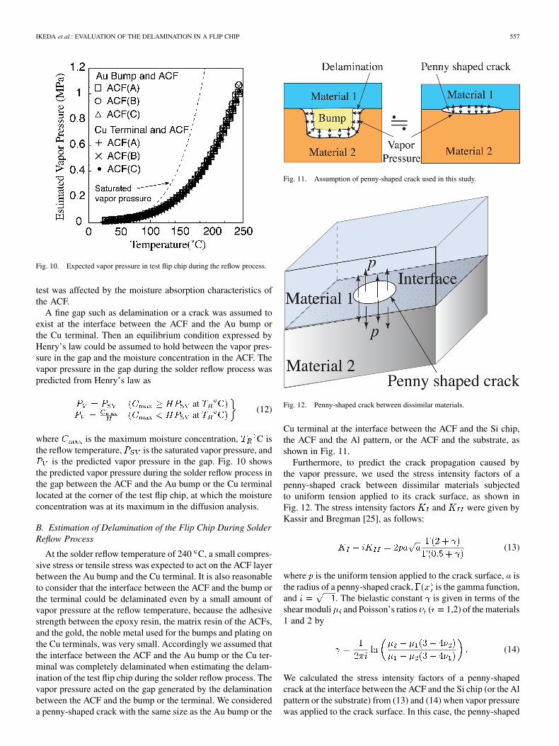
At the solder reflow temperature of 240 C, a small compres-sive stress or tensile stress was expected to act on the ACF layerbetween the Au bump and the Cu terminal. It is also reasonableto consider that the interface between the ACF and the bump orthe terminal could be delaminated even by a small amount ofvapor pressure at the reflow temperature, because the adhesivestrength between the epoxy resin, the matrix resin of the ACFs,and the gold, the noble metal used for the bumps and plating onthe Cu terminals, was very small. Accordingly we assumed thatthe interface between the ACF and the Au bump or the Cu ter-minal was completely delaminated when estimating the delam-ination of the test flip chip during the solder reflow process. Thevapor pressure acted on the gap generated by the delaminationbetween the ACF and the bump or the terminal. We considereda penny-shaped crack with the same size as the Au bump or the
Fig. 11. Assumption of penny-shaped crack used in this study.
Fig. 12. Penny-shaped crack between dissimilar materials.
Cu terminal at the interface between the ACF and the Si chip,the ACF and the Al pattern, or the ACF and the substrate, asshown in Fig. 11.
Furthermore, to predict the crack propagation caused bythe vapor pressure, we used the stress intensity factors of apenny-shaped crack between dissimilar materials subjectedto uniform tension applied to its crack surface, as shown inFig. 12. The stress intensity factors and were given byKassir and Bregman [25], as follows:
(13)
where is the uniform tension applied to the crack surface, isthe radius of a penny-shaped crack, is the gamma function,and . The bielastic constant is given in terms of theshear moduli and Poisson’s ratios ( 1,2) of the materials1 and 2 by
(14)
We calculated the stress intensity factors of a penny-shapedcrack at the interface between the ACF and the Si chip (or the Alpattern or the substrate) from (13) and (14) when vapor pressurewas applied to the crack surface. In this case, the penny-shaped

558 IEEE TRANSACTIONS ON COMPONENTS AND PACKAGING TECHNOLOGIES, VOL. 29, NO. 3, SEPTEMBER 2006
Fig. 13. Comparison between the delamination toughness and the stressintensity factors during the reflow process after the moisture absorption test(K ; Total stress intensity factors caused by vapor pressure in a penny-shapedcrack,K ; Delamination toughness measured by delamination test at 240 C).(a) ACF(A). (b) ACF(B). (c) ACF(C).
crack was the same size 50 m as the gold bump and theCu terminal. Fig. 13 shows the comparison between the stressintensity factor caused by the predicted vapor pressureduring the solder reflow process and the delamination tough-ness measured by the delamination test using the openingdelamination specimen at 240 C. It is found from the figurethat the values of the stress intensity factor are almost thesame for any combinations of materials 1 and 2.
The results of ACF(A) show that the stress intensity factorsof the interface crack between the ACF and the Si chip and be-tween the ACF and the substrate caused by the vapor pressureduring the solder reflow process were lower than the delamina-tion toughness at 240 C. On the other hand, the stress intensityfactor of the interface crack between the ACF and the Al pat-tern caused by the vapor pressure was slightly higher than thedelamination toughness at 240 C. Consequently, the delamina-tion in the test flip chip interconnected by ACF(A) was expectedto propagate along the interface between the ACF and the Al pat-tern from the bottom of the Au bump due to the vapor pressureduring the solder reflow process after moisture absorption. Oncethe interface between the ACF and the Al pattern was delami-nated, the delamination propagated along the interface betweenthe ACF and the Si chip until the vapor pressure was releasedfrom the test flip chip.
In the case of system B interconnected by ACF(B), the valuesof the delamination toughness for all the jointed interfaces werehigher than the stress intensity factors caused by the vapor pres-
sure during the reflow process. So, it is likely that ACF(B) wasnot delaminated. In other words, an initial delamination largerthan the bump radius is required for the propagation of the de-lamination. If we assume that system B had a penny-shapedcrack with a radius of 120 m at the interface between the ACFand the Al pattern, the total stress intensity factor due to thevapor pressure was almost the same as the delamination tough-ness of the interface crack between the ACF and the Al pat-tern. Therefore, we could presume that the disconnected testflip chips of the system B shown in Table IV had a delamina-tion or void equivalent to a penny-shaped crack with a radiusof 120 m at the interface between the ACF and the Al pattern.Similarly, if we presume that the test flip chip of ACF(C) hada penny-shaped crack with a radius of 100 m at the interfacebetween the ACF and the substrate around the copper terminal,the delamination condition would be satisfied. The results pre-dicted by the quantitative estimation method presented in thisstudy can explain the results of the moisture/reflow sensitivitytests shown in Table IV.
V. CONCLUSION
To estimate the moisture/reflow delamination of a flip chipinterconnected by an ACF, we performed moisture/reflowsensitivity tests on test flip chips, conducted moisture diffusionanalyses, and performed tests to measure the delaminationtoughness of ACF joints. The conclusions of the present studyare as follows.
1) We can evaluate the delamination strength of ACF jointsby using the delamination toughness defined by the totalstress intensity factor of an interface crack between dis-similar materials at the onset of delamination. Such de-lamination toughness can be utilized in the practical de-sign of electronic packaging.
2) We can estimate the vapor pressure of a flip chip duringthe solder reflow process after moisture absorption by amoisture diffusion analysis of the flip chip.
3) The moisture/reflow sensitivity tests of test flip chipsshow that a large scale of delamination occurs, resultingin electric disconnection, when the stress intensity factorcaused by the vapor pressure during the reflow processafter moisture absorption exceeds the fracture toughnessof the ACF joint. Such a method can be applied to preventthe delamimation of ACF joints in electronic packaging.
4) The ACF is a viscoelastic material around , and is aviscoplastic material at high temperatures. However, inthis study we only took account of the temperature de-pendence of the elastic properties of the ACF because theheating rate is very high in the case of the solder reflowprocess, and it is kept at the reflow temperature for only40 s. In this short period, the deformation is dominatedrelatively more by elasticity than viscosity. Moreover, theACF layer is very thin, and this layer is constrained by theSi chip and the substrate. Therefore, the effect of viscosityis relatively small on the opening of a crack by vapor pres-sure. If we consider the shear deformation of the ACF dueto thermal stress, the viscosity of the ACF must be takeninto account.

IKEDA et al.: EVALUATION OF THE DELAMINATION IN A FLIP CHIP 559
REFERENCES
[1] H. Kristiansen and J. Liu, “Overview of conductive adhesive intercon-nection technologies for LCDs,” IEEE Trans. Comp., Packag., Manu-fact. Technol. A, vol. 21, no. 2, pp. 208–214, Jun. 1998.
[2] M. J. Yim and K. W. Paik, “Design and understanding of anisotropic con-ductive films (ACFs) for LCD packaging,” IEEE Trans. Comp. , Packag.,Manufact. Technol. A, vol. 21, no. 2, pp. 226–234, Jun. 1998.
[3] K. Suzuki, O. Suzuki, and M. Komagata, “Conductive adhesive mate-rials for lead solder replacement,” IEEE Trans. Comp., Packag., Manu-fact. Technol. A, vol. 21, no. 2, pp. 252–258, Jun. 1998.
[4] J. C. Jagt, “Reliability of electrically conductive adhesive joints for sur-face mount applications; a summary of the state of art,” IEEE Trans.Comp., Packag., Manufact. Technol. A, vol. 21, no. 2, pp. 215–225, Jun.1998.
[5] U. Behner, R. Haug, R. Schütz, and H. Hartnagel, “Characteriztion ofanisotropically conductive adhesive interconnections by 1=f noise mea-surement,” IEEE Trans. Comp., Packag., Manufact. Technol. A, vol. 21,no. 2, pp. 243–247, Jun. 1998.
[6] G. Reza, “Chip scale package issues,” Microelectron. Rel., vol. 40, pp.1157–1161, 2000.
[7] Y. W. Chiu, Y. C. Chan, and S. M. Lui, “Study of short-circuitingbetween adjacent joints under electric effects in fine pitch anisotropicconductive adhesive interconnects,” Microelectron. Rel., vol. 42, pp.1945–1951, 2002.
[8] M. Teo, S. G. Mhaisalkar, E. H. Wong, P. S. Teo, C. C. Wong, K. Ong,C. F. Goh, and L. K. Teh, “Correlation of material properties to reli-ability performance of anisotropic conductive adhesive flip chip pack-ages,” IEEE Trans. Comp., Packag., Manufact. Technol. A, vol. 28, no.1, pp. 157–164, Mar. 2005.
[9] C. Y. Yin, M. O. Alam, T. C. Chan, C. Bailey, and H. Lu, “The effectof reflow process on the contact resistance and reliability of anisotropicconductive film interconnection for flip chip on flex applications,” Mi-croelectron. Rel., vol. 43, pp. 625–633, 2003.
[10] A. Seppala and E. Ristolainen, “Study of adhesive flip chip bondingprocess and failure mechanism of ACA joints,” Microelectron. Rel., vol.44, pp. 639–648, 2004.
[11] T. Hattori, S. Sakata, and G. Murakami, “A stress singularity parameterapproach for evaluating the interfacial reliability of plastic encapsulatedLSI devices,” ASME J. Electron. Packag., vol. 111, pp. 243–245, 1989.
[12] T. Ikeda, I. Arase, Y. Ueno, and N. Miyazaki, “Strength evaluation ofelectronic plastic packaging using stress intensity factors of V-notch,”Comput. Model. Simul. Eng., vol. 1, pp. 91–97, 2000.
[13] T. Ikeda, I. Arase, Y. Ueno, N. Miyazaki, N. Ito, M. Nakatake, andM. Sato, “Strength evaluation of plastic packages under solder reflowprocess using stress intensity factors of V-notch,” J. Electron. Packag.,vol. 125, pp. 31–38, 2003.
[14] G. W. Kim and K. Y. Lee, “Improving the reliability of a plastic ICpackage in the reflow soldering process by DOE,” Solder. Surf. MountTechnol., pp. 40–48, 2005.
[15] F. Erdogan, “Stress distribution in a nonhomogeneous elastic plan withcrack,” J. Appl. Mech., vol. 30, pp. 232–236, 1963.
[16] J. R. Rice, “Elastic fracture mechanics concepts for interfacial crack,” J.Appl. Mech., vol. 55, pp. 98–103, 1988.
[17] T. Ikeda, N. Miyazaki, and T. Soda, “Mixed mode fracture criteria ofinterface crack between dissimilar materials,” Eng. Fracture Mech., vol.45, pp. 725–735, 1998.
[18] B. Malyshev and R. Salganik, “The strength of adhesive joints using thetheory of cracks,” Int. J. Fract. Mech., vol. 1, pp. 114–119, 1965.
[19] W. K. Kim, T. Ikeda, and N. Miazaki, “Reliability evaluation of flipchip using stress intensity factors of an interface crack,” in Proc. Inter-PACK03, 2003, pp. 1–7.
[20] INSPEC, Properties of Silicon, EMIS Data Reviews Series, no. 4, p. 14,1988.
[21] T. Ikeda and C. T. Sun, “Stress intensity factor analysis for an interfacecrack between dissimilar isotropic materials under thermal stress,” Int.J. Fract., vol. 111, pp. 229–249, 2001.
[22] N. Miyazaki, T. Ikeda, T. Soda, and T. Munakata, “Stress intensity factoranalysis of interface crack using boundary element method (Applicationof virtual crack extension method),” JSME Int. J., vol. 36, pp. 36–42,1993.
[23] , “Stress intensity factor analysis of interface crack using boundaryelement method—application of contour-integral method,” Eng. Fract.Mech., vol. 45, pp. 599–610, 1993.
[24] M. Houzawa, M. Toda, K. Kikuchi, T. Yonemoto, and T. Tsukada, Cre-ative Chemical Engineering Course 6, Diffusion and Transport Phe-nomena. Tokyo, Japan: Baifu-kan, 1996.
[25] M. K. Kassir and A. M. Bregman, “The stress intensity factors for pennyshaped crack between two dissimilar materials,” J. Appl. Mech., vol. 39,pp. 308–310, 1972.
Toru Ikeda received the B.S., M.S., and Ph.D.degrees in chemical engineering from Kyushu Uni-versity, Fukuoka, Japan, in 1986, 1988, and 1992,respectively.
After his doctoral study, he spent four years as aResearch Associate and eight years as an AssociateProfessor in Kyushu University. He has been an As-sociate Professor with the Department of MechanicalEngineering and Science, Kyoto University, Kyoto,Japan, since 1994. He has published over 50 journalpapers and over 30 conference papers in the area of
electronic packaging and fracture mechanics. His research interests are the inter-facial fracture mechanics, reliability of electronic packages, and computationalmechanics.
Dr. Ikeda received the Encouragement Award for Young Researchers fromthe Division of Composite, Society of Material Science, Japan, in 1997, theBest Paper Award from the Japan Institute of Electronic Packaging in 2002, andthe JSME Funai Award in 2004.
Won-Keun Kim received the B.S. and M.S. degreesfrom the Department of Material Science, PukyungUniversity, Pusan, Korea, in 1998 and 2000, respec-tively, and the Ph.D. degrees in engineering fromKyushu University, Fukuoka, Japan, in 2004.
He has published 12 journal papers and conferencepapers in the area of material science and electronicpackaging. He currently works for InterconnectProduct & Technology, Samsung Electronics Co.,Ltd., Seoul, Korea. His research interests are todevelop materials and processes in the field of
electronic packaging.
Noriyuki Miyazaki received the B.E. and M.E. de-grees in nuclear engineering and the Ph.D. in engi-neering from The University of Tokyo, Tokyo, Japan,in 1972, 1974, and 1977, respectively.
After working in the Japan Atomic Energy Re-search Institute for six years, he joined KyushuUniversity, Fukuoka, Japan, in 1983. He spent 21years at Kyushu University as an Associate Professorand a Professor in the Department of ChemicalEngineering. He has been a Professor with theDepartment of Mechanical Engineering and Science,
Kyoto University, Kyoto, Japan, since 2004. He has published over 175 journalpapers and over 85 conference papers. He is a member of the editorial boardof the International Journal of Pressure Vessels and Piping, the InternationalJournal of Computational Methods, and the JSME International Journal. Hisresearch interests lie in the fields of computational solid mechanics and fracturemechanics, especially, their application to the mechanical strength studiesof single crystals for electronic/optical devices and the reliability studies ofelectronic packaging.
Dr. Miyazaki received several awards from the Japan Society of Mechan-ical Engineers (JSME), the Japan Institute of Electronic Packaging (JIEP), andthe International Conference on Computational Engineering Science (ICES).He served as a member of General Council for Asian Pacific Association forComputational Mechanics, and as the Co-Chair of the International Conferenceconcerning electronic packaging, 2005 InterPACK Conference, and the 7th In-ternational Conference on Electronics Materials and Packaging (EMAP’05).