Embed Size (px)
Citation preview
1
Evaluation of Hybrid Memory Technologies usingSOT-MRAM for On-Chip Cache Hierarchy
Fabian Oboril, Rajendra Bishnoi, Mojtaba Ebrahimi and Mehdi B. Tahoori
Abstract—Magnetic Random Access Memory (MRAM) is avery promising emerging memory technology because of itsvarious advantages such as non-volatility, high density andscalability. In particular, Spin Orbit Torque (SOT) MRAM isgaining interest as it comes along with all the benefits of itspredecessor Spin Transfer Torque (STT) MRAM, but is supposedto eliminate some of its shortcomings. Especially the split of readand write paths in SOT-MRAM promises faster access timesand lower energy consumption compared to STT-MRAM. Inthis work, we provide a very detailed analysis of SOT-MRAMat both circuit- and architecture-level. We present a detailedevaluation of performance and energy related parameters andcompare the novel SOT-MRAM with several other memorytechnologies. Our architecture-level analysis shows that a hybrid-combination of SRAM for the L1-Data-cache, SOT-MRAM forthe L1-Instruction-cache and L2-cache can reduce the energyconsumption by 60 % while the performance increases by 1 %compared to an SRAM-only configuration. Moreover, the reten-tion failure probability of SOT-MRAM is 27x smaller than theprobability of radiation-induced Soft Errors in SRAM, for a65 nm technology node. All of these advantages together makeSOT-MRAM a viable choice for microprocessor caches.
Index Terms—spin orbit torque, non-volatile memory, cache,hybrid, magnetic memory, reliability, failure rate
I. INTRODUCTION
As the continuous downscaling of CMOS technologybecomes more and more challenging, the microelectronicindustry makes huge efforts to find feasible alternatives.For random access memory (RAM), nano-magnetic stor-age devices (MRAM) are very promising candidates to re-place the traditional CMOS-based memory solutions. Espe-cially the non-volatility of MRAM is a major advantage,which minimizes static power consumption and paves theway towards normally-off/instant-on computing. In particular,MRAM based on Magnetic Tunnel Junction(MTJ) [1, 2]storage devices is one of the most interesting candidates asidentified by the ITRS [3]. Among these memory technologies,Spin Transfer Torque MRAM (STT-MRAM) [4] gains a lot ofattention as it is non-volatile, scalable, and has a low readaccess time [2, 5, 6]. In addition, due to the high resistance ofthe MTJ storage elements, STT-MRAM is compatible with
Manuscript received July 25, 2014; revised September 12, 2014; ac-cepted December 2, 2014.This work was partly supported by the EuropeanCommission under the Seventh Framework Program as part of the spOt project(http://www.spot-research.eu/).
The authors are with Karlsruhe Institute of Technology (KIT), Germany,76131 Karlsruhe. E-mail: {fabian.oboril,rajendra.bishnoi,mojtaba.ebrahimi,mehdi.tahoori}@kit.edu
Copyright (c) 2015 IEEE. Personal use of this material is permitted.However, permission to use this material for any other purposes must beobtained from the IEEE by sending an email to [email protected].
the CMOS process [7]. Furthermore, the magnetization ofthe storage layer, and hence the stored data, can be switchedwithout requiring an external magnetic field. Instead, a spinpolarized current flowing through the MTJ device is employed.
Despite all these advantages, STT-MRAM also faces variouschallenges. First, although the write current is much lower thanin many other MRAM technologies [6], it is still very high,leading to a high energy consumption (10x more energy perwrite operation than SRAM) [8, 9]. In addition, the high cur-rent through the MTJ imposes a severe stress for the memorycell. As a result, it leads to a time dependent degradation ofthe MTJ performance parameters such as tunneling magnetoresistance, write current, and write latency [10]. Moreover, thelifetime is reduced, as the MTJ oxide is threatened by timedependent dielectric breakdown [11, 12]. Second, beside thehigh write current, the write path itself is also a challenge.In STT-MRAM, the read and write operations share thesame access path (through the junction) which can impairthe reliability (read disturb), i.e. a read operation can bymistake lead to a bit flip (magnetization of the storage layer isswitched) [13]. Third, the long write latencies usually prohibitthe use of STT-MRAM in first level caches [5].
To mitigate these issues, Spin Orbit Torque MRAM (SOT-MRAM) has been recently proposed [7, 14, 15]. SOT-MRAMuses a three terminal MTJ-based concept to isolate the readand the write path compared to the two terminal concept ofSTT-MRAM. As a result, in SOT-MRAM the read and thewrite path are perpendicular to each other which significantlyimproves the read stability [7, 16]. Moreover, the write currentis much lower and also the write access is supposed to be muchfaster, as the write path can now be optimized independently.
To evaluate the concept of SOT-MRAM and its implicationsat various design levels, we provide in this paper a detailedcircuit- and architecture-level analysis of SOT-MRAM in bothmemory array design and its implications for a hybrid memoryhierarchy in an advanced computing system. As we will show,the read and write latencies of SOT-MRAM are comparableto those of SRAM. In addition, SOT-MRAM offers a muchhigher density, lower energy consumption, is radiation immuneand non-volatile. All of these aspects make SOT-MRAM aviable candidate for on-chip memory, not only for the last-level cache, but also for lower levels of cache.
A preliminary version of this work was published in [17].In this paper, we extend our preliminary work with a quantita-tive reliability analysis. Therefore, we compare the radiation-induced soft error rate of an SRAM-based cache with the errorrate due to retention failures as well as read disturb faults forSOT-MRAM and STT-MRAM. In addition, we provide a more

2
detailed performance and energy analysis for various hybridcache configurations and evaluate the impact of SOT-MRAMon the instruction and data caches.
To illustrate the benefits of SOT-MRAM, we perform bothcircuit-level and architecture-level evaluations in which wecompare SOT-MRAM with SRAM and STT-MRAM as L1-and L2-cache memory. The main results of this analysis canbe summarized as follows:
1) A hybrid-combination of SRAM for the L1-Data-cache,SOT-MRAM for the L1-Instruction-cache and L2-cacheis 1 % faster compared to an SRAM-only solution. Inaddition, it reduces the energy consumption by 60 % andthe area by 30 %.
2) An SOT-MRAM implementation is the most energyefficient solution saving up to 71 %.
3) Using the area advantage of SOT-MRAM one can dou-ble the size of the L2-cache, which results in 6 % moreperformance, while still saving 56 % of energy comparedto an SRAM-only approach with small L2-cache.
4) Due to the performance advantage of SOT-MRAM overSTT-MRAM, retention failures are less likely in SOT-MRAM. In a 65 nm technology node the failure prob-ability is 27x lower than the probability of radiation-induced soft errors in SRAM. However, the scalingprojections indicate that in future technology nodes, theretention failure rate in SOT-MRAM will be comparablewith the soft error rate in SRAM. Therefore, designersneed to find suitable means to keep the retention failureprobability on an acceptable level. In this case, SOT-MRAM is a fast and very reliable technology.
The rest of this paper is organized as follows. In Section II,the basics of SOT-MRAM are introduced. Section III explainsthe details of the memory architecture using SOT-MRAMand the resulting memory characteristics. Furthermore, theextracted data is compared with various other memory tech-nologies. In addition, this information is used in Section IVto analyze SOT-MRAM as a possible replacement of SRAMinside a classical memory hierarchy. Afterwards, a quantitativereliability comparison of SRAM and SOT-MRAM is presentedin Section V. Finally, Section VI concludes the paper.
II. BACKGROUND
A. Magnetic Tunnel Junction Device
The storage device in Spin Orbit Torque memories is aMagnetic Tunnel Junction (MTJ) cell in which data is stored asa resistance state value. An MTJ device, as shown in Figure 1,consists of two independent ferromagnetic layers (e.g. CoFeB)separated by a very thin (a few nm) barrier oxide layer suchas magnesium oxide (MgO) [7]. One of the two ferromagneticlayers has a fixed magnetization, i.e. the orientation of itsmagnetic field is fixed. Hence, this layer is known as fixedor reference layer. In contrast, in the second magnetic layer,the magnetization can be freely rotated based on the currentdirection (i.e. spin of the electric particles) flowing through theMTJ device. Therefore, this layer is referred to as free layer.
When the direction of the magnetic field of the free layeris parallel (P) to the fixed layer, i.e. the magnetic field
Parallel State (P)(low resistance)
Anti-Parallel State (AP)(high resistance)
fixedLayer
freeLayer
fixedLayer
freeLayer
MgO MgO
Fig. 1. MTJ resistance according to the magnetization of the free layer
orientations in both layers are the same, the MTJ cell hasa low resistance value. Instead, when the magnetization of thefree layer is opposite or anti-parallel (AP) to the fixed layer,the MTJ cell has a high resistance value. This high and lowresistance values are used to represent logic ’1’ and ’0’ values.
B. SOT-MRAM Bit-Cell StructureThe MTJ cell is the core part of a bit-cell in SOT-based
memories as well as in STT-MRAM as shown in Figure 2.However, to eliminate the shortcomings of STT-MRAM, theSOT-MRAM bit-cell has an additional terminal to separate the(unidirectional) read and the (bidirectional) write path whichare perpendicular to each other. The terminals comprise a readline, a write line, a source line and a word line. The wordline is used to access the required bit-cell during memoryaccesses via the NMOS-based access transistor. If such anaccess is a read operation, the source line is connected tothe ground and the read line is used to measure the MTJresistance by sensing the current flowing through the MTJcell. During the write operation the current flows between thesource line and the write line. In fact, the current direction isdetermined by the potentials of the source line and the writeline (i.e. the write path is bidirectional). The current directionin turn affects the magnetization of the free layer and hencethe value stored in the bit-cell. If the current flows from thesource line to the write line, the MTJ resistance will be low.To achieve a high MTJ resistance, the current needs to flowfrom write to source line (high potential for the write line).However, the underlying physical relation between the currentand the magnetic field orientation is still under discussion. Onthe one hand, the Rashba effect is said to be responsible for thecurrent-induced magnetization switch [14, 18]. On the otherhand, many people explain this phenomenon with the SpinHall Effect [15], and hence refer to SOT-MRAM as “GiantSpin Hall Effect” MRAM. Nevertheless, in both cases the spin-
FixedLayer
Bit Line:Read\W
rite
FreeLayer
WordLine Access Transistor
Read&
Write
Path
Source Line: Read & Write
(a) STT-MRAM (b) SOT-MRAM
WordLine Access Transistor
Source Line
Write Line
Write PathRead
Path
ReadLine
Fig. 2. Bit-cell for STT-MRAM and SOT-MRAM
3
orbit-torque is responsible for the free layer magnetization,which is the origin of the name SOT-MRAM.
It can be inferred from Figure 2 that a bit-cell consists of twodifferent technologies, namely CMOS for the transistor and anano-magnetic technology for the MTJ device. Therefore, itrequires additional layers in the layout and more processingsteps during fabrication.
C. Comparison of SOT-MRAM and STT-MRAM
The main difference between STT-MRAM and SOT-MRAMis that SOT-MRAM has separate paths for read and writeoperations. Hence, these paths can be also optimized indepen-dently. This can be used to reduce the write current and writelatency in SOT-MRAM compared to STT-MRAM. As we willshow later, this is the reason why SOT-MRAM can achieveaccess times similar to SRAM, while STT-MRAM suffersfrom high write latencies. In addition, the asymmetry betweenread and write operations can be significantly reduced, suchthat in SOT-MRAM read and write operations have similaraccess times, while in STT-MRAM a write access requiresconsiderably more time.
Furthermore, the probability of read disturb, i.e. that a readoperation accidentally flips the bit-cell value, is negligiblein SOT-MRAM [7, 16] due to the separated read and writepaths, as well as the MTJ design, while it is an importantsource of unreliability in STT-MRAM [19]. In fact, in STT-MRAM the current for writing ’0’ (’P’ state) and the readcurrent share the same path and are in the same direction,which can cause read disturb. In contrast, in SOT-MRAM, thewrite path is always perpendicular to the read path, whichavoids read disturb faults. Read disturb is also the reason,why in STT-MRAM read and write paths cannot be optimizedindependently, while this is possible in SOT-MRAM. In STT-MRAM it is very important to maintain a certain ratio betweenthe read and the write current, to avoid high read disturb rates.If the read current is increased to achieve a better readability(reduced read error rate), the write current has to be increasedas well, as otherwise the read disturb rate would increase. Thesame problem arises, if the write current should be reduced toreduce the write energy. In this case, the read current needsto be lowered as well, which however impairs the readabil-ity. In contrast, since in SOT-MRAM read and write pathsare separated, the read and write currents can be optimizedindependently to co-optimize readability, access latencies andenergy consumption. This tuning of the paths is achieved bydesigning the read and write circuitries accordingly (i.e. usesmaller/larger transistors to reduce/increase the current)
A common reliability challenge of SOT-MRAM and STT-MRAM is the retention failure, which is due to an inherentthermal instability of the MTJ cells [19]. This thermal insta-bility can lead to data loss which reduces the retention time.
Note that in this work the in-plane STT-MRAM technol-ogy is employed for our experimental analysis. Beside thisimplementation, there is also a perpendicular STT-MRAMsolution. The difference between these two approaches isthat in in-plane STT-MRAM the magnetic orientations of theMTJ layers are orthogonal to the current direction (read orwrite), while these are in parallel to the current direction
(read or write) in the perpendicular implementation. Therefore,the latter version typically requires less write current and ismore energy efficient [4, 20]. In fact, the reported currentdata and switching latencies vary a lot in literature. For in-plane STT-MRAM the typical write current is in the rangeof 100 uA-1000 uA with switching latencies between 2 ns and12 ns [11, 21–27], while for perpendicular STT-MRAM thewrite current is usually between 30 uA-300 uA with writelatencies in the range of 0.4 ns-45 ns [4, 20, 21, 28–31]. Inthis regard, always more current leads to lower write latenciesfor all STT-MRAM and SOT-MRAM approaches. The modelfor in-plane STT-MRAM used in this work is based on realsilicon data [23] and requires a write current of 525 uA with aswitching time of 10.5 ns (see Section III-B1 for more details),which is in the range of the previously mentioned data.
In both STT-MRAM approaches there is a considerableasymmetry between read and write delays as well as betweenthe switching time from P→AP and AP→P [27, 28], whichis not the case for SOT-MRAM. In addition, the read andwrite paths are shared and hence, even the perpendicularSTT-MRAM version cannot achieve the same efficiency asSOT-MRAM, where read and write paths can be optimizedindependently [7]. Moreover, in SOT-MRAM the write pathhas a much lower resistance as the write path in STT-MRAM,which is going through the MTJ cell [7]. Thus, higher currentscan be used for SOT-MRAM to allow faster write operations.In contrast, increasing the write current in STT-MRAM maylead to accelerated wearout of the MTJ cell. In addition, theswitching behavior in SOT-MRAM is free of incubation asit is a surface effect relying on spin orbit torque, whereasin STT-MRAM the incubation time can significantly increasethe switching speed [32]. As a result, if perpendicular STT-MRAM is used instead of in-plane, the STT-MRAM resultsshown in Section III and Section IV can improve, but not reachto the level of SOT-MRAM.
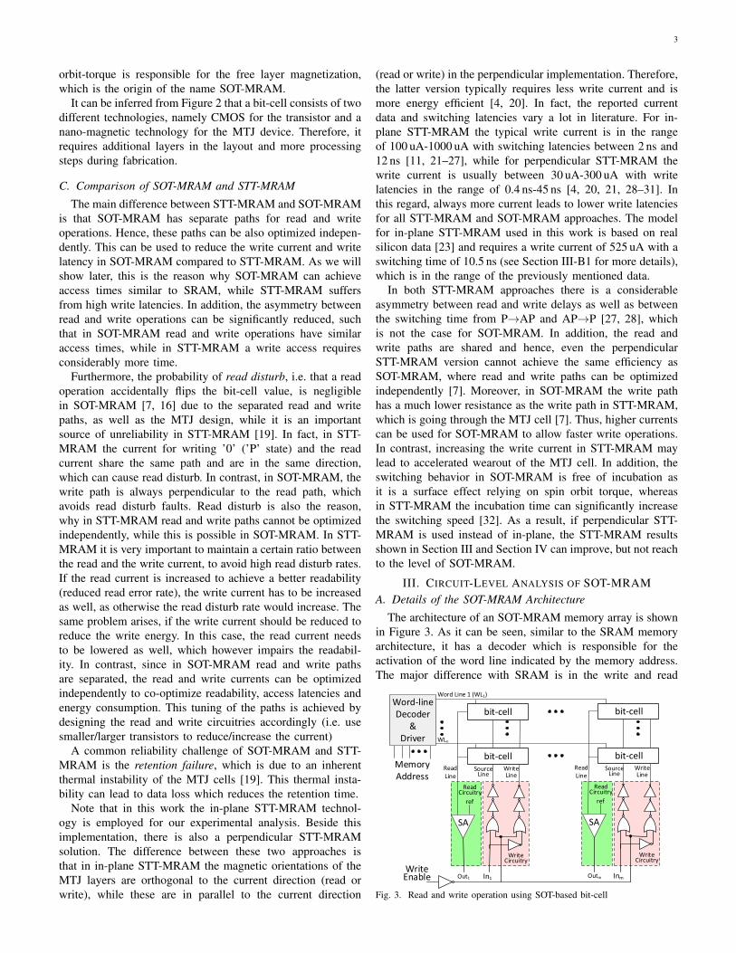
III. CIRCUIT-LEVEL ANALYSIS OF SOT-MRAMA. Details of the SOT-MRAM Architecture
The architecture of an SOT-MRAM memory array is shownin Figure 3. As it can be seen, similar to the SRAM memoryarchitecture, it has a decoder which is responsible for theactivation of the word line indicated by the memory address.The major difference with SRAM is in the write and read
Memory Address
Read Line
Source Line
Write Line
WLn
ref
In1
Write Enable Out1
bit-cell
bit-cell
Word Line 1 (WL1)
Write Circuitry
Read Circuitry
SA
Read Line
Source Line
Write Line
ref
InmOutm
bit-cell
bit-cell
Write Circuitry
Read Circuitry
Word-line Decoder
&Driver
SA
Fig. 3. Read and write operation using SOT-based bit-cell
4
SOT-MRAM STT-MRAMRead Latency [ps] 221 226Write Latency [ps] 266 10,500 (reset) / 3,700 (set)Write Current [uA] 100 525 (reset) / 616 (set)Read Energy [pJ] 1.8 1.8Write Energy [pJ] 0.1 3.9 (reset) / 3.4 (set)
TABLE ICOMPARISON OF SOT-MRAM AND STT-MRAM FOR A SINGLE BIT-CELL
WITH ONE ACCESS TRANSISTOR
circuitry. As mentioned in Section II, the SOT bit-cell is afour terminal device which has different paths for write andread operations. In case the write enable signal is inactive,a read operation is performed by connecting the read line ofthe desired bit-cell to the corresponding sense amplifier. Thecurrent sensed on the read line is compared with a referencevalue to distinguish the value stored in the bit-cell.
For the write operation, the write enable signal has tobe activated. In fact, the write operation in SOT-MRAM isbidirectional, i.e. the data stored in the bit-cell depends onthe direction of the current which in-turn is determined bythe input data value. As a result, the write circuitry can bedesigned in such a way that the high resistance state of theMTJ cell represents either a logic ’1’ or a logic ’0’. For thewrite circuitry shown in Figure 3, it is assumed that the anti-parallel state (high resistance) represents a logical value of ’1’.When the write enable signal is active and the input data hasa logical value of ’1’, the current flows from the write line tothe source line in the MTJ cell resulting in high resistance.
B. Comparison with Other Memory Technologies
To investigate the SOT based memory architecture andcompare it with other memory technologies, we use a multi-level approach. First, we analyze the behavior for a singlebit-cell only. Afterwards, this information is used to extractthe data for an entire memory array.
1) Circuit-Level Memory Evaluation Platform: For the bit-cell analysis of SOT-MRAM, we use the framework proposedin [7] in combination with the TSMC 65 nm general purposelibrary for the CMOS elements. For STT-MRAM we apply themodel from [23], which employs in-plane magnetization. Forboth technologies, the models are based on real silicon data [7,22, 23, 41], and the switching dynamics for the free layers aredescribed by the Landau-Lifshitz-Gilbert model [42].
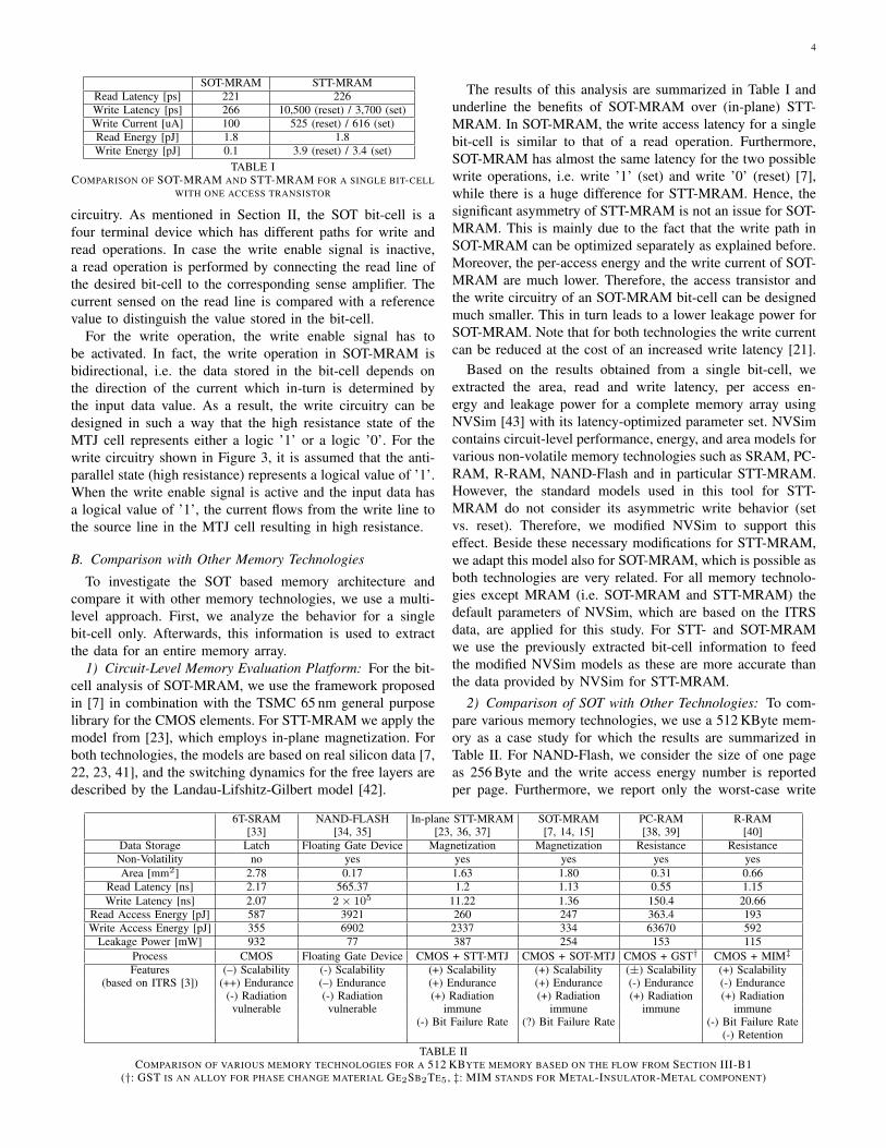
The results of this analysis are summarized in Table I andunderline the benefits of SOT-MRAM over (in-plane) STT-MRAM. In SOT-MRAM, the write access latency for a singlebit-cell is similar to that of a read operation. Furthermore,SOT-MRAM has almost the same latency for the two possiblewrite operations, i.e. write ’1’ (set) and write ’0’ (reset) [7],while there is a huge difference for STT-MRAM. Hence, thesignificant asymmetry of STT-MRAM is not an issue for SOT-MRAM. This is mainly due to the fact that the write path inSOT-MRAM can be optimized separately as explained before.Moreover, the per-access energy and the write current of SOT-MRAM are much lower. Therefore, the access transistor andthe write circuitry of an SOT-MRAM bit-cell can be designedmuch smaller. This in turn leads to a lower leakage power forSOT-MRAM. Note that for both technologies the write currentcan be reduced at the cost of an increased write latency [21].
Based on the results obtained from a single bit-cell, weextracted the area, read and write latency, per access en-ergy and leakage power for a complete memory array usingNVSim [43] with its latency-optimized parameter set. NVSimcontains circuit-level performance, energy, and area models forvarious non-volatile memory technologies such as SRAM, PC-RAM, R-RAM, NAND-Flash and in particular STT-MRAM.However, the standard models used in this tool for STT-MRAM do not consider its asymmetric write behavior (setvs. reset). Therefore, we modified NVSim to support thiseffect. Beside these necessary modifications for STT-MRAM,we adapt this model also for SOT-MRAM, which is possible asboth technologies are very related. For all memory technolo-gies except MRAM (i.e. SOT-MRAM and STT-MRAM) thedefault parameters of NVSim, which are based on the ITRSdata, are applied for this study. For STT- and SOT-MRAMwe use the previously extracted bit-cell information to feedthe modified NVSim models as these are more accurate thanthe data provided by NVSim for STT-MRAM.
2) Comparison of SOT with Other Technologies: To com-pare various memory technologies, we use a 512 KByte mem-ory as a case study for which the results are summarized inTable II. For NAND-Flash, we consider the size of one pageas 256 Byte and the write access energy number is reportedper page. Furthermore, we report only the worst-case write
6T-SRAM NAND-FLASH In-plane STT-MRAM SOT-MRAM PC-RAM R-RAM[33] [34, 35] [23, 36, 37] [7, 14, 15] [38, 39] [40]
Data Storage Latch Floating Gate Device Magnetization Magnetization Resistance ResistanceNon-Volatility no yes yes yes yes yesArea [mm2] 2.78 0.17 1.63 1.80 0.31 0.66
Read Latency [ns] 2.17 565.37 1.2 1.13 0.55 1.15Write Latency [ns] 2.07 2× 10⁵ 11.22 1.36 150.4 20.66
Read Access Energy [pJ] 587 3921 260 247 363.4 193Write Access Energy [pJ] 355 6902 2337 334 63670 592
Leakage Power [mW] 932 77 387 254 153 115Process CMOS Floating Gate Device CMOS + STT-MTJ CMOS + SOT-MTJ CMOS + GST† CMOS + MIM‡
Features (–) Scalability (-) Scalability (+) Scalability (+) Scalability (±) Scalability (+) Scalability(based on ITRS [3]) (++) Endurance (–) Endurance (+) Endurance (+) Endurance (-) Endurance (-) Endurance
(-) Radiation (-) Radiation (+) Radiation (+) Radiation (+) Radiation (+) Radiationvulnerable vulnerable immune immune immune immune
(-) Bit Failure Rate (?) Bit Failure Rate (-) Bit Failure Rate(-) Retention
TABLE IICOMPARISON OF VARIOUS MEMORY TECHNOLOGIES FOR A 512 KBYTE MEMORY BASED ON THE FLOW FROM SECTION III-B1
(†: GST IS AN ALLOY FOR PHASE CHANGE MATERIAL GE2SB2TE5 , ‡: MIM STANDS FOR METAL-INSULATOR-METAL COMPONENT)
5
latency and energy (with respect to set/reset operations andlocation of the bit-cell). As the results show, SOT-MRAMis comparable to SRAM in terms of performance and iseven superior when it comes to energy consumption and celldensity. In addition, unlike SRAM, SOT-MRAM does not havescalability limitations [4] and can be considered as radiationimmune. Although PC-RAM and R-RAM are comparable toSOT-MRAM in terms of area and read latency, these memorytechnologies suffer from their high write latency and writeenergy [44]. NAND-Flash has the smallest area and leakage,however it has problems with a high write energy, scalabilityand endurance.
Please note that for every memory technology differentways of implementation are possible, e.g. low-power, high-performance or high-density optimized versions. As a con-sequence, also the absolute numbers presented in Table IIwould change for other implementations. However, the majortrends will remain the same. Therefore, the main purpose ofthis analysis, as summarized in Table II, is a comparativeanalysis of the trends for several memory technologies andtheir usabilities for the on-chip memory hierarchy, rather thanthe actual numbers.
In terms of cost, STT-MRAM and hence also SOT-MRAMshould reach a similar price per GBit compared to DRAM,when these technologies enter the mass production phase [45].Consequently, both MRAM technologies will be cheaper thanSRAM, although additional processing steps are required.However, these will be compensated by the higher density.
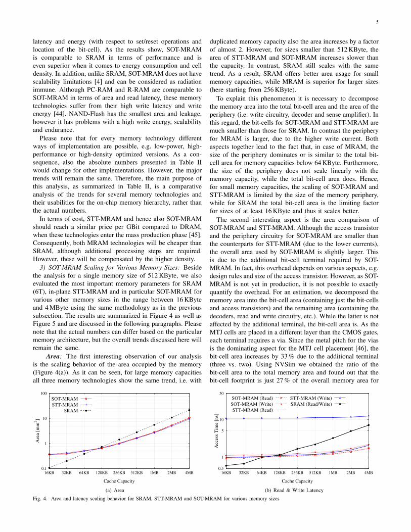
3) SOT-MRAM Scaling for Various Memory Sizes: Besidethe analysis for a single memory size of 512 KByte, we alsoevaluated the most important memory parameters for SRAM(6T), in-plane STT-MRAM and in particular SOT-MRAM forvarious other memory sizes in the range between 16 KByteand 4 MByte using the same methodology as in the previoussubsection. The results are summarized in Figure 4 as well asFigure 5 and are discussed in the following paragraphs. Pleasenote that the actual numbers can differ based on the particularmemory architecture, but the overall trends discussed here willremain the same.
Area: The first interesting observation of our analysisis the scaling behavior of the area occupied by the memory(Figure 4(a)). As it can be seen, for large memory capacitiesall three memory technologies show the same trend, i.e. with
duplicated memory capacity also the area increases by a factorof almost 2. However, for sizes smaller than 512 KByte, thearea of STT-MRAM and SOT-MRAM increases slower thanthe capacity. In contrast, SRAM still scales with the sametrend. As a result, SRAM offers better area usage for smallmemory capacities, while MRAM is superior for larger sizes(here starting from 256 KByte).
To explain this phenomenon it is necessary to decomposethe memory area into the total bit-cell area and the area of theperiphery (i.e. write circuitry, decoder and sense amplifier). Inthis regard, the bit-cells for SOT-MRAM and STT-MRAM aremuch smaller than those for SRAM. In contrast the peripheryfor MRAM is larger, due to the higher write current. Bothaspects together lead to the fact that, in case of MRAM, thesize of the periphery dominates or is similar to the total bit-cell area for memory capacities below 64 KByte. Furthermore,the size of the periphery does not scale linearly with thememory capacity, while the total bit-cell area does. Hence,for small memory capacities, the scaling of SOT-MRAM andSTT-MRAM is limited by the size of the memory periphery,while for SRAM the total bit-cell area is the limiting factorfor sizes of at least 16 KByte and thus it scales better.
The second interesting aspect is the area comparison ofSOT-MRAM and STT-MRAM. Although the access transistorand the periphery circuitry for SOT-MRAM are smaller thanthe counterparts for STT-MRAM (due to the lower currents),the overall area used by SOT-MRAM is slightly larger. Thisis due to the additional bit-cell terminal required by SOT-MRAM. In fact, this overhead depends on various aspects, e.g.design rules and size of the access transistor. However, as SOT-MRAM is not yet in production, it is not possible to exactlyquantify the overhead. For an estimation, we decomposed thememory area into the bit-cell area (containing just the bit-cellsand access transistors) and the remaining area (containing thedecoders, read and write circuitry, etc.). While the latter is notaffected by the additional terminal, the bit-cell area is. As theMTJ cells are placed in a different layer than the CMOS gates,each terminal requires a via. Since the metal pitch for the viasis the dominating aspect for the MTJ cell placement [46], thebit-cell area increases by 33 % due to the additional terminal(three vs. two). Using NVSim we obtained the ratio of thebit-cell area to the total memory area and found out that thebit-cell footprint is just 27 % of the overall memory area for
0.1
1
10
100
16KB 32KB 64KB 128KB 256KB 512KB 1MB 2MB 4MB
Are
a [m
m2]
Cache Capacity
SOT-MRAM
STT-MRAM
SRAM
(a) Area
0.5
1
5
10
50
16KB 32KB 64KB 128KB 256KB 512KB 1MB 2MB 4MB
Acc
ess
Tim
e [n
s]
Cache Capacity
SOT-MRAM (Read)
SOT-MRAM (Write)
STT-MRAM (Read)
STT-MRAM (Write)
SRAM (Read/Write)
(b) Read & Write Latency
Fig. 4. Area and latency scaling behavior for SRAM, STT-MRAM and SOT-MRAM for various memory sizes
6
10
100
1000
10000
16KB 32KB 64KB 128KB 256KB 512KB 1MB 2MB 4MB
Per
-Acc
ess
En
erg
y [
pJ]
Cache Capacity
SOT-MRAM (Read)
SOT-MRAM (Write)
STT-MRAM (Read)
STT-MRAM (Write)
SRAM (Read)
SRAM (Write)
(a) Per-Access Energy
10
100
1000
10000
16KB 32KB 64KB 128KB 256KB 512KB 1MB 2MB 4MB
Lea
kag
e P
ow
er [
mW
]
Cache Capacity
SOT-MRAM
STT-MRAM
SRAM
(b) Leakage Power
Fig. 5. Access energy and leakage scaling behavior for SRAM, STT-MRAM and SOT-MRAM for various memory sizes
a memory size of 512 KByte. Consequently, the additionalterminal increases the total memory area by 9 %. Please notethat this is just a very rough, first order approximation. Inreality, the overhead can be considerably smaller.
Access Latencies: Another interesting phenomenon canbe observed for the scaling behavior of the access latencies(see Figure 4(b)). Since the load capacitance of an SRAM-based bit-cell is much higher than that of an MTJ-based bit-cell, as the latter is much smaller, the access latencies ofSRAM are stronger correlated to the number of bit-cells thanthose of SOT-MRAM or STT-MRAM. For MRAM memories,in the evaluated size range, the major contributor is the latencyof the periphery circuitry and the routing delay. Thus, theaccess latencies of SOT-MRAM and STT-MRAM do notincrease as much as those of SRAM with increasing memorysize. As a result, although SRAM is the fastest memorytechnology for very small memory sizes, it is slower thanSOT-MRAM for both read and write operations for largermemory sizes. While STT-MRAM is comparable to SOT-MRAM in terms of read latency, it suffers from its very longwrite latency. This underlines how effective the separation ofread and write paths and hence their independent optimizationin SOT-MRAM is. As a result, the asymmetric access behavior(almost) disappears.
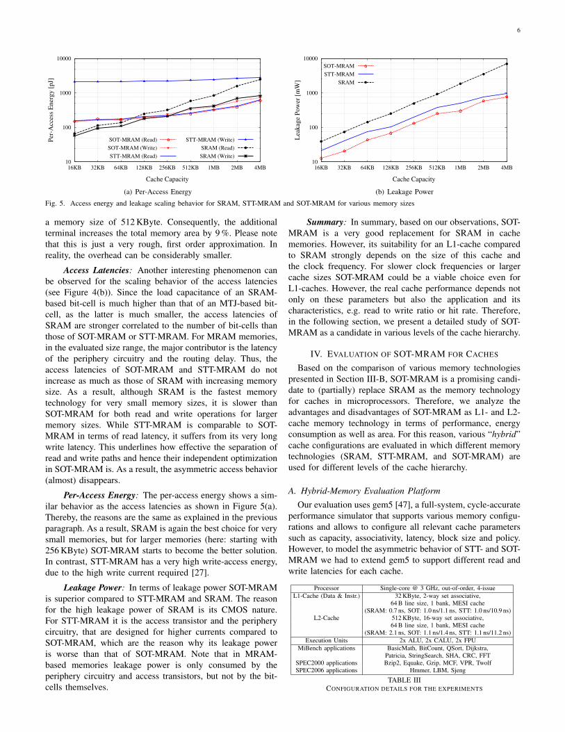
Per-Access Energy: The per-access energy shows a sim-ilar behavior as the access latencies as shown in Figure 5(a).Thereby, the reasons are the same as explained in the previousparagraph. As a result, SRAM is again the best choice for verysmall memories, but for larger memories (here: starting with256 KByte) SOT-MRAM starts to become the better solution.In contrast, STT-MRAM has a very high write-access energy,due to the high write current required [27].
Leakage Power: In terms of leakage power SOT-MRAMis superior compared to STT-MRAM and SRAM. The reasonfor the high leakage power of SRAM is its CMOS nature.For STT-MRAM it is the access transistor and the peripherycircuitry, that are designed for higher currents compared toSOT-MRAM, which are the reason why its leakage poweris worse than that of SOT-MRAM. Note that in MRAM-based memories leakage power is only consumed by theperiphery circuitry and access transistors, but not by the bit-cells themselves.
Summary: In summary, based on our observations, SOT-MRAM is a very good replacement for SRAM in cachememories. However, its suitability for an L1-cache comparedto SRAM strongly depends on the size of this cache andthe clock frequency. For slower clock frequencies or largercache sizes SOT-MRAM could be a viable choice even forL1-caches. However, the real cache performance depends notonly on these parameters but also the application and itscharacteristics, e.g. read to write ratio or hit rate. Therefore,in the following section, we present a detailed study of SOT-MRAM as a candidate in various levels of the cache hierarchy.
IV. EVALUATION OF SOT-MRAM FOR CACHES
Based on the comparison of various memory technologiespresented in Section III-B, SOT-MRAM is a promising candi-date to (partially) replace SRAM as the memory technologyfor caches in microprocessors. Therefore, we analyze theadvantages and disadvantages of SOT-MRAM as L1- and L2-cache memory technology in terms of performance, energyconsumption as well as area. For this reason, various “hybrid”cache configurations are evaluated in which different memorytechnologies (SRAM, STT-MRAM, and SOT-MRAM) areused for different levels of the cache hierarchy.
A. Hybrid-Memory Evaluation Platform
Our evaluation uses gem5 [47], a full-system, cycle-accurateperformance simulator that supports various memory configu-rations and allows to configure all relevant cache parameterssuch as capacity, associativity, latency, block size and policy.However, to model the asymmetric behavior of STT- and SOT-MRAM we had to extend gem5 to support different read andwrite latencies for each cache.
Processor Single-core @ 3 GHz, out-of-order, 4-issueL1-Cache (Data & Instr.) 32 KByte, 2-way set associative,
64 B line size, 1 bank, MESI cache(SRAM: 0.7 ns, SOT: 1.0 ns/1.1 ns, STT: 1.0 ns/10.9 ns)
L2-Cache 512 KByte, 16-way set associative,64 B line size, 1 bank, MESI cache
(SRAM: 2.1 ns, SOT: 1.1 ns/1.4 ns, STT: 1.1 ns/11.2 ns)Execution Units 2x ALU, 2x CALU, 2x FPU
MiBench applications BasicMath, BitCount, QSort, Dijkstra,Patricia, StringSearch, SHA, CRC, FFT
SPEC2000 applications Bzip2, Equake, Gzip, MCF, VPR, TwolfSPEC2006 applications Hmmer, LBM, Sjeng
TABLE IIICONFIGURATION DETAILS FOR THE EXPERIMENTS
7
0
20
40
60
80
100
120
140
160
SRA
M+SR
AM
SRA
M+STT
SRA
M+SO
T
STT+SRA
M
STT+STT
STT+SOT
SOT+SR
AM
SOT+STT
SOT+SO
T
SRA
M+SR
AM
SRA
M+STT
SRA
M+SO
T
STT+SRA
M
STT+STT
STT+SOT
SOT+SR
AM
SOT+STT
SOT+SO
T
SRA
M+SR
AM
SRA
M+STT
SRA
M+SO
T
STT+SRA
M
STT+STT
STT+SOT
SOT+SR
AM
SOT+STT
SOT+SO
T
No
rmal
ized
to
SR
AM
+S
RA
M
SRAM+SOT means: L1D/I SRAM L2 SOT-MRAM
Area Runtime Energy Consumption
Leakage EnergyRead EnergyWrite Energy
RuntimeArea
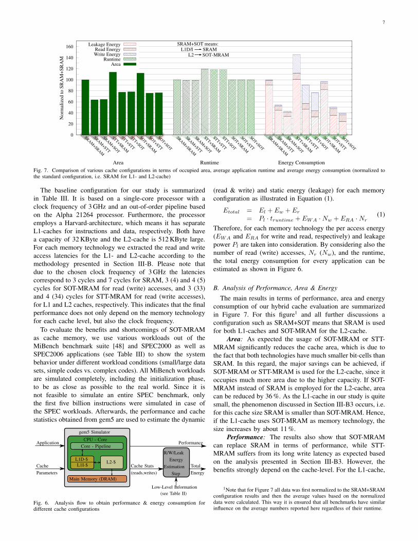
Fig. 7. Comparison of various cache configurations in terms of occupied area, average application runtime and average energy consumption (normalized tothe standard configuration, i.e. SRAM for L1- and L2-cache)
The baseline configuration for our study is summarizedin Table III. It is based on a single-core processor with aclock frequency of 3 GHz and an out-of-order pipeline basedon the Alpha 21264 processor. Furthermore, the processoremploys a Harvard-architecture, which means it has separateL1-caches for instructions and data, respectively. Both havea capacity of 32 KByte and the L2-cache is 512 KByte large.For each memory technology we extracted the read and writeaccess latencies for the L1- and L2-cache according to themethodology presented in Section III-B. Please note thatdue to the chosen clock frequency of 3 GHz the latenciescorrespond to 3 cycles and 7 cycles for SRAM, 3 (4) and 4 (5)cycles for SOT-MRAM for read (write) accesses, and 3 (33)and 4 (34) cycles for STT-MRAM for read (write accesses),for L1 and L2 caches, respectively. This indicates that the finalperformance does not only depend on the memory technologyfor each cache level, but also the clock frequency.
To evaluate the benefits and shortcomings of SOT-MRAMas cache memory, we use various workloads out of theMiBench benchmark suite [48] and SPEC2000 as well asSPEC2006 applications (see Table III) to show the systembehavior under different workload conditions (small/large datasets, simple codes vs. complex codes). All MiBench workloadsare simulated completely, including the initialization phase,to be as close as possible to the real world. Since it isnot feasible to simulate an entire SPEC benchmark, onlythe first five billion instructions were simulated in case ofthe SPEC workloads. Afterwards, the performance and cachestatistics obtained from gem5 are used to estimate the dynamic
gem5 Simulator
CPU - Core
L1D-$L1I-$
L2-$
Core - Pipeline
Main Memory (DRAM)
Application
CacheParameters
Cache Stats(reads,writes)
Low-Level Information(see Table II)
R/W/LeakEnergy
EstimationStep
Performance
TotalEnergy
Fig. 6. Analysis flow to obtain performance & energy consumption fordifferent cache configurations
(read & write) and static energy (leakage) for each memoryconfiguration as illustrated in Equation (1).
Etotal = El + Ew + Er= Pl · truntime + EWA ·Nw + ERA ·Nr
(1)
Therefore, for each memory technology the per access energy(EWA and ERA for write and read, respectively) and leakagepower Pl are taken into consideration. By considering also thenumber of read (write) accesses, Nr (Nw), and the runtime,the total energy consumption for every application can beestimated as shown in Figure 6.
B. Analysis of Performance, Area & Energy
The main results in terms of performance, area and energyconsumption of our hybrid cache evaluation are summarizedin Figure 7. For this figure1 and all further discussions aconfiguration such as SRAM+SOT means that SRAM is usedfor both L1-caches and SOT-MRAM for the L2-cache.
Area: As expected the usage of SOT-MRAM or STT-MRAM significantly reduces the cache area, which is due tothe fact that both technologies have much smaller bit-cells thanSRAM. In this regard, the major savings can be achieved, ifSOT-MRAM or STT-MRAM is used for the L2-cache, since itoccupies much more area due to the higher capacity. If SOT-MRAM instead of SRAM is employed for the L2-cache, areacan be reduced by 36 %. As the L1-cache in our study is quitesmall, the phenomenon discussed in Section III-B3 occurs, i.e.for this cache size SRAM is smaller than SOT-MRAM. Hence,if the L1-cache uses SOT-MRAM as memory technology, thesize increases by about 11 %.
Performance: The results also show that SOT-MRAMcan replace SRAM in terms of performance, while STT-MRAM suffers from its long write latency as expected basedon the analysis presented in Section III-B3. However, thebenefits strongly depend on the cache-level. For the L1-cache,
1Note that for Figure 7 all data was first normalized to the SRAM+SRAMconfiguration results and then the average values based on the normalizeddata were calculated. This way it is ensured that all benchmarks have similarinfluence on the average numbers reported here regardless of their runtime.
8
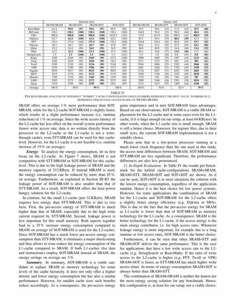
Runtime [ms] Energy [mJ]SRAM+SRAM SRAM+STT SRAM+SOT SOT+SOT SRAM+SRAM SRAM+STT SRAM+SOT SOT+SOT
BasicMath 61.4 59.8 (97) 59.8 (97) 60.5 (99) 74.5 39.6 (53) 31.5 (42) 29.5 (40)BitCount 130.1 130.1 (100) 130.1 (100) 130.1 (100) 146.8 76.0 (52) 58.6 (40) 48.4 (33)
CRC 998.8 998.8 (100) 998.8 (100) 1025.5 (103) 1175 631.9 (54) 498.5 (42) 458.5 (39)Dijkstra 62.7 62.4 (100) 62.4 (100) 62.6 (100) 83.3 49.0 (59) 40.6 (49) 42.9 (52)
FFT 176.1 175.4 (100) 175.3 (100) 176.1 (100) 216.8 120.4 (56) 96.8 (45) 93.7 (43)Patricia 49.1 46.7 (95) 46.7 (95) 47.6 (97) 60.6 31.6 (52) 25.3 (42) 24.1 (40)QSort 35.2 34.9 (99) 34.9 (99) 34.9 (99) 40.0 20.9 (52) 16.0 (40) 13.4 (33)SHA 23.3 23.3 (100) 23.3 (100) 23.3 (100) 29.4 16.8 (57) 13.6 (46) 13.7 (46)
StringSearch 1.5 1.5 (100) 1.5 (100) 1.5 (101) 1.9 1.0 (56) 0.8 (45) 0.8 (45)Bzip2 2382 2369 (99) 2369 (99) 2372 (100) 2908 1605 (55) 1287 (44) 1233 (42)Gzip 1826 1810 (99) 1810 (99) 1814 (99) 2211 1212 (55) 962 (44) 905 (41)Twolf 5189 5130 (99) 5126 (99) 5148 (99) 5944 3086 (52) 2392 (40) 2046 (34)VPR 3754 3709 (99) 3706 (99) 3715 (99) 4281 2204 (51) 1703 (40) 1430 (33)
Equake 5070 5017 (99) 5015 (99) 5025 (99) 5724 2927 (51) 2255 (39) 1865 (33)MCF 3213 3174 (99) 3172 (99) 3179 (99) 3520 1749 (50) 1323 (38) 1018 (29)
Hmmer 1395 1370 (98) 1369 (98) 1378 (99) 1752 976 (56) 788 (45) 781 (45)LBM 5303 5275 (99) 5273 (99) 5275 (99) 5909 3168 (54) 2301 (39) 1834 (31)Sjeng 2219 2196 (99) 2195 (99) 2201 (99) 2733 1515 (55) 1209 (44) 1160 (42)
Average 100 % 99 % 99 % 100 % 100 % 54 % 42 % 39 %
TABLE IVPER BENCHMARK ANALYSIS OF DIFFERENT “HYBRID” CACHE CONFIGURATION (BOLD NUMBERS REPRESENT THE BEST VALUE, NUMBERS IN ()
REPRESENT PERCENTAGE VALUES BASED ON SRAM+SRAM)
SRAM offers on average 1 % more performance than SOT-MRAM, while for the L2-cache SOT-MRAM is slightly faster,which results in a slight performance increase (i.e. runtimereduction) of 1 % on average. Since the write access latency ofthe L2-cache has less effect on the overall system performance(lower write access rate, data is no written directly from theprocessor to the L2-cache as the L1-cache is not a write-through cache), even STT-MRAM can be used for this cache-level. However, for the L1-cache it is not feasible (i.e. runtimeincrease of 19 % on average).
Energy: To analyze the energy consumption, let us firstfocus on the L2-cache. As Figure 7 shows, SRAM is notcompetitive with STT-MRAM or SOT-MRAM for this cache-level. This is due to the high leakage power of SRAM and thememory capacity of 512 KByte. If instead MRAM is used,the energy consumption can be reduced by more than 45 %,on average. Furthermore, as explained in Section III-B3 theleakage power of SOT-MRAM is also smaller than that ofSTT-MRAM. As a result, SOT-MRAM offers the least powerhungry solution for the L2-cache.
In contrast, for the small L1-cache (just 32 KByte), SRAMrequires less energy than STT-MRAM. This is due to twofacts. First, the per-access energy of STT-MRAM is muchhigher than that of SRAM, especially due to the high writecurrent required by STT-MRAM. Second, leakage power isless important for this small memory. Both aspects togetherlead to a 35 % increase energy consumption compared toSRAM on average (if SOT-MRAM is used for the L2-cache).Since SOT-MRAM has a much lower per-access energy con-sumption than STT-MRAM, it eliminates a major shortcomingand thus allows to even reduce the energy consumption of theL1-cache compared to SRAM. If both L1-caches (for dataand instructions) employ SOT-MRAM instead of SRAM, theenergy savings on average are 3 %.
Summary: In summary, SOT-MRAM is a viable can-didate to replace SRAM as memory technology for somelevels of the cache hierarchy. It does not only offer a higherdensity and lower energy consumption but has also a similarperformance. However, for smaller cache sizes such benefitsreduce accordingly. As a consequence, the per-access energy
gains importance and in turn SOT-MRAM loses advantages.Based on our observations, SOT-MRAM is a viable SRAM re-placement for the L2-cache and in some cases even for the L1-cache, if it is large enough (in our setup, at least 64 KBytes). Inother words, when the L1-cache size is small enough, SRAMis still a better choice. Moreover, for register files, due to theirsmall sizes, the current SOT-MRAM implementation is not asuitable choice.
Please note that in a low-power processor running at amuch lower clock frequency than the one used in this study,the access time differences between SRAM, SOT-MRAM andSTT-MRAM are less significant. Therefore, the performancedifferences are also less pronounced.
1) In-Depth Evaluation: In Table IV the results per bench-mark for the hybrid cache-configurations SRAM+SRAM,SRAM+STT, SRAM+SOT and SOT+SOT are shown. As itcan be seen, SOT+SOT is in most situations the solution withthe lowest energy consumption, regardless of the applicationruntime. Hence it is the best choice for low power systems.However, for some applications the combination of SRAMfor the L1-cache and SOT-MRAM for the L2-cache offersa slightly better energy efficiency (e.g. Dijkstra or SHA).This is due to the fact that the per-access energy for SRAMas L1-cache is lower than that of SOT-MRAM as memorytechnology for the L1-cache. As a consequence, SRAM is thebetter technology for the L1-cache, if the access energy is themain energy contributor, i.e. for high access rates. Wheneverleakage energy is more important, for example due to a longruntime or low access rates, SOT-MRAM is the better choice.
Furthermore, it can be seen that often SRAM+STT andSRAM+SOT deliver the same performance. This is the casefor applications that have a low write access rate to the L2-cache (e.g. StringSearch or BasicMath). If the ratio of writeaccess to the L2-cache is higher (e.g. FFT, Twolf or VPR)SRAM+SOT is faster, as STT-MRAM has much higher writeaccess times. In terms of energy consumption SRAM+SOT isalways better than SRAM+STT.
The combination of SRAM+SRAM is neither the fastest northe most energy saving solution for any benchmark. Hence,this configuration is, at least for our setup, not a viable choice.
9
Instead a hybrid solution or SOT-MRAM-only is favorable.However, considering all aspects, i.e. performance, energy andarea, the hybrid solutions offers the best trade-off for ourprocessor configuration.
C. Using SOT-MRAM Advantages for Larger Caches
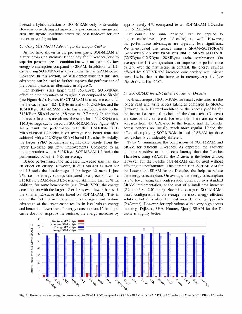
As we have shown in the previous parts, SOT-MRAM isa very promising memory technology for L2-caches, due tosuperior performance in combination with an extremely lowenergy consumption compared to SRAM. In addition an L2-cache using SOT-MRAM is also smaller than an SRAM-basedL2-cache. In this section, we will demonstrate that this areaadvantage can be used to further improve the performance ofthe overall system, as illustrated in Figure 8.
For memory sizes larger than 256 KByte, SOT-MRAMoffers an area advantage of roughly 2.3x compared to SRAM(see Figure 4(a)). Hence, if SOT-MRAM is used, one can dou-ble the cache size (1024 KByte instead of 512 KByte), and the1024 KByte SOT-MRAM cache has a size comparable to the512 KByte SRAM cache (2.8 mm2 vs. 2.7 mm2). In addition,the access latencies are almost the same for a 512 KByte and1 MByte large cache based on SOT-MRAM (see Figure 4(b)).As a result, the performance with the 1024 KByte SOT-MRAM-based L2-cache is on average 6 % better than thatachieved with a 512 KByte SRAM-based L2-cache. Especially,the larger SPEC benchmarks significantly benefit from thelarger L2-cache (up 35 % improvement). Compared to animplementation with a 512 KByte SOT-MRAM L2-cache theperformance benefit is 5 %, on average.
Beside performance, the increased L2-cache size has alsoan effect on energy. However, if SOT-MRAM is used forthe L2-cache the disadvantage of the larger L2-cache is just2 %, i.e. the energy savings compared to a processor with a512 KByte SRAM-based L2-cache are still more than 55 %. Inaddition, for some benchmarks (e.g. Twolf, VPR), the energyconsumption with the larger L2-cache is even lower than withthe smaller L2-cache (both based on SOT-MRAM). This isdue to the fact that in these situations the significant runtimeadvantage of the larger cache results in less leakage energyand hence in a lower overall energy consumption. If the largercache does not improve the runtime, the energy increases by
approximately 4 % (compared to an SOT-MRAM L2-cachewith 512 KByte).
Of course, the same principal can be applied tohigher cache-levels (e.g. L3-cache) as well. However,the performance advantages are typically less significant.We investigated this aspect using a SRAM+SOT+SRAM(32 KByte+512 KByte+64 MByte) and a SRAM+SOT+SOT(32 KByte+512 KByte+128 MByte) cache combination. Onaverage, the last configuration can improve the performanceby 2 % over the first setup. In contrast, the energy savingsoffered by SOT-MRAM increase considerably with highercache-levels, due to the increase in memory capacity (seeFig. 5(a) and Fig. 5(b)).
D. SOT-MRAM for L1-Cache: I-cache vs. D-cache
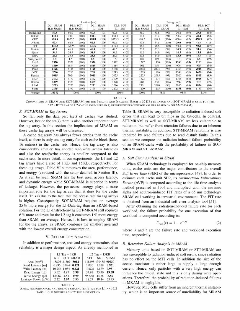
A disadvantage of SOT-MRAM for small cache sizes are thelonger read and write access latencies compared to SRAM.However, in a Harvard-architecture the access profiles forthe instruction cache (I-cache) and the data cache (D-cache)are considerably different. For example, there are no writeaccesses from the CPU-side to the I-cache and the I-cacheaccess patterns are usually much more regular. Hence, theeffect of employing SOT-MRAM instead of SRAM for thesetwo caches is considerably different.
Table V summarizes the comparison of SOT-MRAM andSRAM for different L1-caches. As expected, the D-cacheis more sensitive to the access latency than the I-cache.Therefore, using SRAM for the D-cache is the better choice.However, for the I-cache SOT-MRAM can be used withoutaffecting the performance. This combination, SOT-MRAM forthe I-cache and SRAM for the D-cache, also helps to reducethe energy consumption. On average, the energy consumptionis 7 % lower using this configuration compared to a standardSRAM implementation, at the cost of a small area increase(2.24 mm2 vs. 2.05 mm2). Nevertheless a pure SOT-MRAM-based configuration is on average the most energy efficientsolution, but it is also the most area demanding approach(2.43 mm2). However, for applications with a very high accessrate (e.g. Dijkstra, SHA, Hmmer, Sjeng) SRAM for the D-cache is slightly better.
0
10
20
30
40
50
60
70
80
BasicM
ath
BitC
nts
CRC
Dijkstra
FFTPatricia
Qsort
SHA
StringSearch
Bzip2
Gzip
Twolf
VPR
Equake
MCF
Hm
mer
LBM
Sjeng
Average
Imp
rovem
ent
ov
er 5
12
KB
yte
SR
AM
[%
]
Runtime 512 KByteRuntime 1024 KByte
Energy 512 KByteEnergy 1024 KByte
Fig. 8. Performance and energy improvements for SRAM+SOT compared to SRAM+SRAM with 1) 512 KByte L2-cache and 2) with 1024 KByte L2-cache
10
Runtime [ms] Energy [mJ]DL1: SRAM DL1: SOT DL1: SRAM DL1: SOT DL1: SRAM DL1: SOT DL1: SRAM DL1: SOTIL1: SRAM IL1: SRAM IL1: SOT IL1: SOT IL1: SRAM IL1: SRAM IL1: SOT IL1: SOT
BasicMath 59.8 60.0 (100) 60.3 (101) 60.5 (101) 31.7 30.8 (97) 30.8 (97) 29.8 (94)BitCnts 130.1 130.1 (100) 130.1 (100) 130.1 (100) 58.6 53.4 (91) 53.6 (91) 48.4 (83)
CRC 998.8 1025.5 (103) 998.8 (100) 1025.5 (103) 498.5 498.1 (100) 460.4 (92) 458.5 (92)Dijkstra 62.4 62.6 (100) 62.4 (100) 62.6 (100) 40.6 44.5 (110) 39.0 (96) 42.9 (106)
FFT 175.3 175.9 (100) 175.6 (100) 176.1 (100) 96.9 96.5 (100) 94.3 (97) 93.8 (97)Patricia 46.7 46.8 (100) 47.4 (102) 47.6 (102) 25.6 25.3 (99) 24.9 (97) 24.6 (96)Qsort 34.9 34.9 (100) 34.9 (100) 34.9 (100) 16.0 14.9 (94) 14.5 (91) 13.4 (84)SHA 23.3 23.3 (100) 23.3 (100) 23.3 (100) 13.6 14.0 (103) 13.3 (97) 13.7 (100)
StringSearch 1.5 1.5 (101) 1.5 (100) 1.5 (101) 0.8 0.9 (104) 0.8 (95) 0.8 (99)Bzip2 2370 2372 (100) 2370 (100) 2372 (100) 1287 1320 (103) 1200 (93) 1233 (96)Gzip 1810 1814 (100) 1810 (100) 1814 (100) 962 959 (100) 909 (94) 905 (94)Twolf 5126 5146 (100) 5126 (100) 5148 (100) 2392 2274 (96) 2164 (90) 2046 (86)VPR 3706 3715 (100) 3706 (100) 3715 (100) 1703 1586 (93) 1548 (91) 1430 (84)
Equake 5015 5024 (100) 5015 (100) 5025 (100) 2255 2095 (93) 2026 (90) 1865 (83)MCF 3172 3179 (100) 3172 (100) 3179 (100) 1323 1174 (89) 1168 (88) 1018 (77)
Hmmer 1369 1378 (101) 1369 (100) 1378 (101) 788 833 (106) 736 (93) 782 (99)LBM 5273 5276 (100) 5273 (100) 5276 (100) 2301 2080 (90) 2055 (89) 1834 (80)Sjeng 2195 2197 (100) 2199 (100) 2202 (100) 1209 1215 (100) 1155 (96) 1160 (96)
Average 100 % 100 % 100 % 100 % 100 % 98 % 93 % 91 %
TABLE VCOMPARISON OF SRAM AND SOT-MRAM FOR THE I-CACHE AND D-CACHE; EACH IS 32 KBYTE LARGE AND SOT-MRAM IS USED FOR THE
512 KBYTE LARGE L2-CACHE (NUMBERS IN () REPRESENT PERCENTAGE VALUES BASED ON SRAM/SRAM)
E. SOT-MRAM in Tag ArraysSo far, only the data part (set) of caches was studied.
However, beside the set(s) there is also another important part:the tag array. In this section the implications of MRAM onthese cache tag arrays will be discussed.
A cache tag array has always fewer entries than the cacheitself, as there is only one tag entry for each cache block (here,16 entries) in the cache sets. Hence, the tag array is alsoconsiderably smaller, has shorter read/write access latenciesand also the read/write energy is smaller compared to thecache sets. In more detail, in our experiments, the L1 and L2tag arrays have a size of 1 KB and 15 KB, respectively. Forthese tag arrays, Table VI summarizes the area, performance,and energy (extracted with the setup detailed in Section III).As it can be seen, SRAM has the best area, access latency,and dynamic energy while SOT-MRAM is superior in termsof leakage. However, the per-access energy plays a moreimportant role for the tag arrays than it does for the cacheitself. This is due to the fact, that the access rate for tag arraysis higher. Consequently, SOT-MRAM requires on average25 % more energy for the L1-Data-tag than an SRAM-basedsolution. For the L1-Instruction-tag SOT-MRAM still requires6 % more and even for the L2-tag it consumes 1 % more energythan SRAM, on average. Hence, it is best to employ SRAMfor the tag arrays, as SRAM combines the smallest area andwith the lowest overall energy consumption.
V. RELIABILITY ANALYSIS
In addition to performance, area and energy constraints, alsoreliability is a major design aspect. As already mentioned in
L1 Tag = 1KB L2 Tag = 15KBSTT SOT SRAM STT SOT SRAM
Area [µm2] 18896 21307 8012 118495 139485 90030Read Latency [ns] 0.895 0.894 0.421 1.020 1.019 0.951Write Latency [ns] 10.754 1.054 0.421 10.898 1.179 0.951Read Energy [pJ] 5.52 4.97 2.98 34.91 33.30 19.58Write Energy [pJ] 126.62 4.51 0.99 957.68 44.38 5.86
Leakage Power [mW] 2.22 2.07 2.96 18.27 18.14 33.43
TABLE VIAREA, PERFORMANCE, AND ENERGY CHARACTERISTICS FOR L1 AND L2
TAGS; BOLD NUMBERS SHOW THE BEST OPTION
Table II, SRAM is very susceptible to radiation-induced softerrors that can lead to bit flips in the bit-cells. In contrast,STT-MRAM as well as SOT-MRAM are less vulnerable toradiation, but suffer from retention failures due to an inherentthermal instability. In addition, STT-MRAM reliability is alsoimpaired by read failures due to read disturb faults. In thissection we compare the radiation-induced failure probabilityof an SRAM cache with the probability of failures in SOT-MRAM and STT-MRAM.
A. Soft Error Analysis in SRAM
When SRAM technology is employed for on-chip memoryunits, cache units are the major contributors to the overallSoft Error Rate (SER) of the microprocessor [49]. In order toestimate each cache unit SER, its Architectural VulnerabilityFactor (AVF) is computed according to the life time analysismethod presented in [50] and multiplied with the intrinsicalpha and neutron-induced FIT rates of a 65 nm technologySRAM cell working in terrestrial environment. The FIT rateis obtained from an industrial soft error analysis tool [51].
After obtaining the radiation-induced failure rate for eachworkload, the failure probability for one execution of thatworkload is computed according to:
Frad(t) = 1− e−λt (2)
where λ and t are the failure rate and workload executiontime, respectively.
B. Retention Failure Analysis in MRAM
Memory units based on SOT-MRAM or STT-MRAM areless susceptible to radiation-induced soft errors, since radiationhas no effect on the MTJ cells. In addition the size of theaccess transistor is rather large to supply a large enoughcurrent. Hence, only particles with a very high energy caninfluence the bit-cell state and this is only during write oper-ations. Therefore, the probability of radiation-induced failuresin MRAM is negligible.
However, MTJ cells suffer from an inherent thermal instabil-ity, which is an important source of unreliability for MRAM
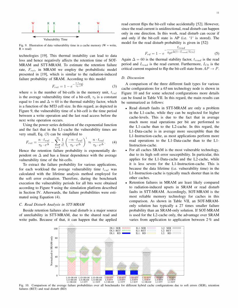
11
W R R R W
Vulnerability Time
Fig. 9. Illustration of data vulnerability time in a cache memory (W = write,R = read)
technologies [19]. This thermal instability can lead to dataloss and hence negatively affects the retention time of SOT-MRAM and STT-MRAM. To estimate the retention failurerate, Fret, in MRAM we employ the probabilistic modelpresented in [19], which is similar to the radiation-inducedfailure probability of SRAM. According to this model
Fret = 1− e−n·tvulτ0·e∆ (3)
where n is the number of bit-cells in the memory unit, tvulis the average vulnerability time of a bit-cell, τ0 is a constantequal to 1 ns and ∆ ≈ 60 is the thermal stability factor, whichis a function of the MTJ cell size. In this regard, as depicted inFigure 9, the vulnerability time of a bit-cell is the time periodbetween a write operation and the last read access before thenext write operation occurs.
Using the power series definition of the exponential functionand the fact that in the L1-cache the vulnerability times arevery small, Eq. (3) can be simplified to
Fret =n · tvulτ0 · e∆
−∞∑i=2
1
i!
(−n · tvulτ0 · e∆
)i≈ n · tvulτ0 · e∆
. (4)
Hence the retention failure probability is exponentially de-pendent on ∆ and has a linear dependence with the averagevulnerability time of the bit-cells.
To extract the failure probability for various applications,for each workload the average vulnerability time tvul wascalculated with the lifetime analysis method employed forthe soft error evaluation. Therefore, during the benchmarkexecution the vulnerability periods for all bits were obtainedaccording to Figure 9 using the simulation platform describedin Section IV. Afterwards, the failure probabilities were esti-mated using Equation (4).
C. Read Disturb Analysis in STT-MRAM
Beside retention failures also read disturb is a major sourceof unreliability in STT-MRAM, due to the shared read andwrite paths. Because of that, it can happen that the applied
read current flips the bit-cell value accidentally [52]. However,since the read current is unidirectional, read disturb can happenonly in one direction. In this work, read disturb can occur ifand only if the bit-cell state is AP (i.e. ‘1‘ is stored). Themodel for the read disturb probability is given in [52]:
Frd = 1− e−
treadτ0e∆(1−Iread/IC0) (5)
Again ∆ = 60 is the thermal stability factor, tread is the readperiod and Iread is the read current. Furthermore, IC0 is thecritical current required to flip the bit-cell state from AP → P .
D. Discussion
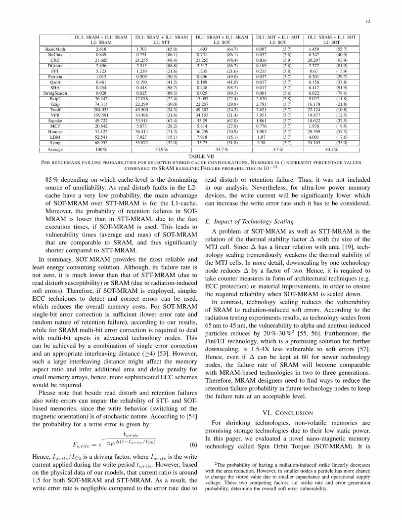
A comparison of the three different fault types for variouscache configurations for a 65 nm technology node is shown inFigure 10 and for some selected configurations more detailscan be found in Table VII. In this regard, the main results canbe summarized as follows:• Read disturb faults in STT-MRAM are only a problem
in the L1-cache, while they can be neglected for highercache-levels. This is due to the fact that in averagemuch more read operations per bit are performed tothe L1-cache than to the L2-cache. In this regard, theL1-Data-cache is in average more susceptible than theL1-Instruction-cache, as most applications perform moreread operations to the L1-Data-cache than to the L1-Instruction-cache.
• For all caches SRAM is the most vulnerable technology,due to its high soft error susceptibility. In particular, thisapplies for the L1-Data-cache and the L2-cache, whileit is less severe for the L1-Instruction-cache. This isbecause the data lifetime (i.e. vulnerability time) in theL1-Instruction-cache is typically much shorter than in theother caches.
• Retention failures in MRAM are least likely comparedto radiation-induced upsets in SRAM or read disturbfaults in STT-MRAM. Accordingly, SOT-MRAM is themost reliable memory technology for caches in thiscomparison. As shown in Table VII, an SOT-MRAM-only solution has typically a 27 times smaller failureprobability than an SRAM-only solution. If SOT-MRAMis used for the L2-cache only, the advantage over SRAMvaries from application to application between 2 % and
0
20
40
60
80
100
L1D-SRAML1I-SRAML2-SRAM
L1D-SRAML1I-SRAM
L2-STT
L1D-SRAML1I-SRAM
L2-SOT
L1D-STTL1I-STT
L2-SRAM
L1D-STTL1I-STTL2-STT
L1D-STTL1I-STTL2-SOT
L1D-SOTL1I-SOT
L2-SRAM
L1D-SOTL1I-SOTL2-STT
L1D-SOTL1I-SOTL2-SOT
Norm
aliz
ed t
o S
RA
M-o
nly
DL1: SERDL1: RETDL1: RD
IL1: SERIL1: RETIL1: RD
L2: SERL2: RETL2: RD
Fig. 10. Comparison of the average failure probabilities over all benchmarks for different hybrid cache configurations due to soft errors (SER), retentionfailures (RET) and read disturb (RD)
12
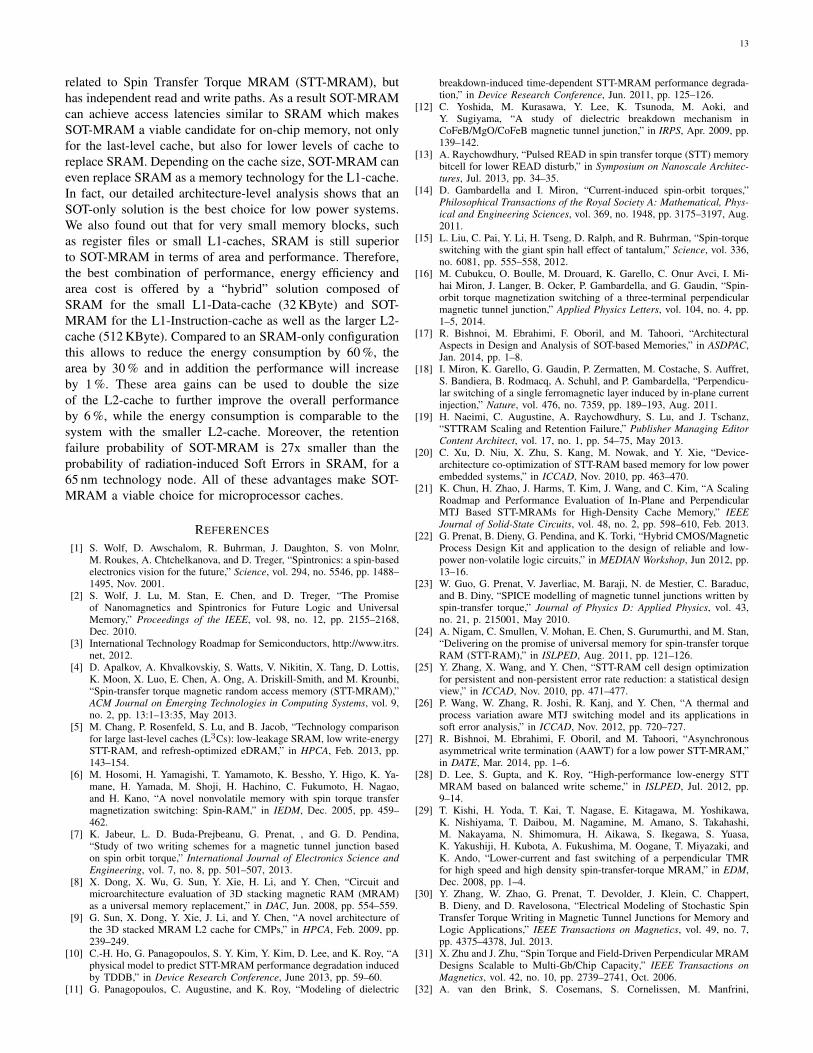
DL1: SRAM + IL1: SRAM DL1: SRAM + IL1: SRAM DL1: SRAM + IL1: SRAM DL1: SOT + IL1: SOT DL1: SRAM + IL1: SOTL2: SRAM L2: STT L2: SOT L2: SOT L2: SOT
BasicMath 2.618 1.703 (65.0) 1.693 (64.7) 0.097 (3.7) 1.459 (55.7)BitCnts 0.849 0.731 (86.1) 0.731 (86.1) 0.032 (3.8) 0.347 (40.9)
CRC 21.605 21.255 (98.4) 21.255 (98.4) 0.836 (3.9) 20.297 (93.9)Dijkstra 2.896 2.513 (86.8) 2.512 (86.7) 0.109 (3.8) 2.372 (81.9)
FFT 5.723 1.239 (21.6) 1.235 (21.6) 0.215 (3.8) 0.67 ( 5.9)Patricia 1.012 0.509 (50.3) 0.496 (49.0) 0.037 (3.7) 0.301 (29.7)Qsort 0.461 0.190 (41.2) 0.189 (41.0) 0.017 (3.7) 0.156 (33.8)SHA 0.454 0.448 (98.7) 0.448 (98.7) 0.017 (3.7) 0.417 (91.9)
StringSearch 0.028 0.025 (89.3) 0.025 (89.3) 0.001 (3.6) 0.022 (78.6)Bzip2 76.342 17.078 (22.4) 17.097 (22.4) 2.870 (3.8) 9.027 (11.8)Gzip 74.313 22.299 (30.0) 22.207 (29.9) 2.783 (3.7) 16.178 (21.8)Twolf 204.033 49.500 (24.3) 49.302 (24.2) 7.621 (3.7) 22.124 (10.8)VPR 159.591 34.498 (21.6) 34.155 (21.4) 5.951 (3.7) 19.877 (12.5)
Equake 49.722 33.511 (67.4) 33.29 (67.0) 1.861 (3.7) 18.622 (37.5)MCF 20.842 5.873 (28.2) 5.814 (27.9) 0.776 (3.7) 1.978 ( 9.5)
Hmmer 51.122 36.414 (71.2) 36.259 (70.9) 1.903 (3.7) 29.399 (57.5)LBM 52.541 7.927 (15.1) 7.918 (15.1) 1.97 (3.7) 4.001 ( 7.6)Sjeng 68.952 35.872 (52.0) 35.73 (51.8) 2.58 (3.7) 24.103 (35.0)
Average 100 % 53.9 % 53.7 % 3.7 % 40.1 %
TABLE VIIPER BENCHMARK FAILURE PROBABILITIES FOR SELECTED HYBRID CACHE CONFIGURATIONS. NUMBERS IN () REPRESENT PERCENTAGE VALUES
COMPARED TO SRAM BASELINE; FAILURE PROBABILITIES IN 10−12
85 % depending on which cache-level is the dominatingsource of unreliability. As read disturb faults in the L2-cache have a very low probability, the main advantageof SOT-MRAM over STT-MRAM is for the L1-cache.Moreover, the probability of retention failures in SOT-MRAM is lower than in STT-MRAM, due to the fastexecution times, if SOT-MRAM is used. This leads tovulnerability times (average and max) of SOT-MRAMthat are comparable to SRAM, and thus significantlyshorter compared to STT-MRAM.
In summary, SOT-MRAM provides the most reliable andleast energy consuming solution. Although, its failure rate isnot zero, it is much lower than that of STT-MRAM (due toread disturb susceptibility) or SRAM (due to radiation-inducedsoft errors). Therefore, if SOT-MRAM is employed, simplerECC techniques to detect and correct errors can be used,which reduces the overall memory costs. For SOT-MRAMsingle-bit error correction is sufficient (lower error rate andrandom nature of retention failure), according to our results,while for SRAM multi-bit error correction is required to dealwith multi-bit upsets in advanced technology nodes. Thiscan be achieved by a combination of single error correctionand an appropriate interleaving distance (≥4) [53]. However,such a large interleaving distance might affect the memoryaspect ratio and infer additional area and delay penalty forsmall memory arrays, hence, more sophisticated ECC schemeswould be required.
Please note that beside read disturb and retention failuresalso write errors can impair the reliability of STT- and SOT-based memories, since the write behavior (switching of themagnetic orientation) is of stochastic nature. According to [54]the probability for a write error is given by:
Fwrite = e−
twriteτ0e∆(1−Iwrite/IC0) (6)
Hence, Iwrite/IC0 is a driving factor, where Iwrite is the writecurrent applied during the write period twrite. However, basedon the physical data of our models, that current ratio is around1.5 for both SOT-MRAM and STT-MRAM. As a result, thewrite error rate is negligible compared to the error rate due to
read disturb or retention failure. Thus, it was not includedin our analysis. Nevertheless, for ultra-low power memorydevices, the write current will be significantly lower whichcan increase the write error rate such it has to be considered.
E. Impact of Technology Scaling
A problem of SOT-MRAM as well as STT-MRAM is therelation of the thermal stability factor ∆ with the size of theMTJ cell. Since ∆ has a linear relation with area [19], tech-nology scaling tremendously weakens the thermal stability ofthe MTJ cells. In more detail, downscaling by one technologynode reduces ∆ by a factor of two. Hence, it is required totake counter measures in form of architectural techniques (e.g.ECC protection) or material improvements, in order to ensurethe required reliability when SOT-MRAM is scaled down.
In contrast, technology scaling reduces the vulnerabilityof SRAM to radiation-induced soft errors. According to theradiation testing experiments results, as technology scales from65 nm to 45 nm, the vulnerability to alpha and neutron-inducedparticles reduces by 20 %-30 %2 [55, 56]. Furthermore, theFinFET technology, which is a promising solution for furtherdownscaling, is 1.5-4X less vulnerable to soft errors [57].Hence, even if ∆ can be kept at 60 for newer technologynodes, the failure rate of SRAM will become comparablewith MRAM-based technologies in two to three generations.Therefore, MRAM designers need to find ways to reduce theretention failure probability in future technology nodes to keepthe failure rate at an acceptable level.
VI. CONCLUSION
For shrinking technologies, non-volatile memories arepromising storage technologies due to their low static power.In this paper, we evaluated a novel nano-magnetic memorytechnology called Spin Orbit Torque (SOT-MRAM). It is
2The probability of having a radiation-induced strike linearly decreaseswith the area reduction. However, in smaller nodes a particle has more chanceto change the stored value due to smaller capacitance and operational supplyvoltage. These two competing factors, i.e. strike rate and error generationprobability, determine the overall soft error vulnerability.
13
related to Spin Transfer Torque MRAM (STT-MRAM), buthas independent read and write paths. As a result SOT-MRAMcan achieve access latencies similar to SRAM which makesSOT-MRAM a viable candidate for on-chip memory, not onlyfor the last-level cache, but also for lower levels of cache toreplace SRAM. Depending on the cache size, SOT-MRAM caneven replace SRAM as a memory technology for the L1-cache.In fact, our detailed architecture-level analysis shows that anSOT-only solution is the best choice for low power systems.We also found out that for very small memory blocks, suchas register files or small L1-caches, SRAM is still superiorto SOT-MRAM in terms of area and performance. Therefore,the best combination of performance, energy efficiency andarea cost is offered by a “hybrid” solution composed ofSRAM for the small L1-Data-cache (32 KByte) and SOT-MRAM for the L1-Instruction-cache as well as the larger L2-cache (512 KByte). Compared to an SRAM-only configurationthis allows to reduce the energy consumption by 60 %, thearea by 30 % and in addition the performance will increaseby 1 %. These area gains can be used to double the sizeof the L2-cache to further improve the overall performanceby 6 %, while the energy consumption is comparable to thesystem with the smaller L2-cache. Moreover, the retentionfailure probability of SOT-MRAM is 27x smaller than theprobability of radiation-induced Soft Errors in SRAM, for a65 nm technology node. All of these advantages make SOT-MRAM a viable choice for microprocessor caches.
REFERENCES
[1] S. Wolf, D. Awschalom, R. Buhrman, J. Daughton, S. von Molnr,M. Roukes, A. Chtchelkanova, and D. Treger, “Spintronics: a spin-basedelectronics vision for the future,” Science, vol. 294, no. 5546, pp. 1488–1495, Nov. 2001.
[2] S. Wolf, J. Lu, M. Stan, E. Chen, and D. Treger, “The Promiseof Nanomagnetics and Spintronics for Future Logic and UniversalMemory,” Proceedings of the IEEE, vol. 98, no. 12, pp. 2155–2168,Dec. 2010.
[3] International Technology Roadmap for Semiconductors, http://www.itrs.net, 2012.
[4] D. Apalkov, A. Khvalkovskiy, S. Watts, V. Nikitin, X. Tang, D. Lottis,K. Moon, X. Luo, E. Chen, A. Ong, A. Driskill-Smith, and M. Krounbi,“Spin-transfer torque magnetic random access memory (STT-MRAM),”ACM Journal on Emerging Technologies in Computing Systems, vol. 9,no. 2, pp. 13:1–13:35, May 2013.
[5] M. Chang, P. Rosenfeld, S. Lu, and B. Jacob, “Technology comparisonfor large last-level caches (L3Cs): low-leakage SRAM, low write-energySTT-RAM, and refresh-optimized eDRAM,” in HPCA, Feb. 2013, pp.143–154.
[6] M. Hosomi, H. Yamagishi, T. Yamamoto, K. Bessho, Y. Higo, K. Ya-mane, H. Yamada, M. Shoji, H. Hachino, C. Fukumoto, H. Nagao,and H. Kano, “A novel nonvolatile memory with spin torque transfermagnetization switching: Spin-RAM,” in IEDM, Dec. 2005, pp. 459–462.
[7] K. Jabeur, L. D. Buda-Prejbeanu, G. Prenat, , and G. D. Pendina,“Study of two writing schemes for a magnetic tunnel junction basedon spin orbit torque,” International Journal of Electronics Science andEngineering, vol. 7, no. 8, pp. 501–507, 2013.
[8] X. Dong, X. Wu, G. Sun, Y. Xie, H. Li, and Y. Chen, “Circuit andmicroarchitecture evaluation of 3D stacking magnetic RAM (MRAM)as a universal memory replacement,” in DAC, Jun. 2008, pp. 554–559.
[9] G. Sun, X. Dong, Y. Xie, J. Li, and Y. Chen, “A novel architecture ofthe 3D stacked MRAM L2 cache for CMPs,” in HPCA, Feb. 2009, pp.239–249.
[10] C.-H. Ho, G. Panagopoulos, S. Y. Kim, Y. Kim, D. Lee, and K. Roy, “Aphysical model to predict STT-MRAM performance degradation inducedby TDDB,” in Device Research Conference, June 2013, pp. 59–60.
[11] G. Panagopoulos, C. Augustine, and K. Roy, “Modeling of dielectric
breakdown-induced time-dependent STT-MRAM performance degrada-tion,” in Device Research Conference, Jun. 2011, pp. 125–126.
[12] C. Yoshida, M. Kurasawa, Y. Lee, K. Tsunoda, M. Aoki, andY. Sugiyama, “A study of dielectric breakdown mechanism inCoFeB/MgO/CoFeB magnetic tunnel junction,” in IRPS, Apr. 2009, pp.139–142.
[13] A. Raychowdhury, “Pulsed READ in spin transfer torque (STT) memorybitcell for lower READ disturb,” in Symposium on Nanoscale Architec-tures, Jul. 2013, pp. 34–35.
[14] D. Gambardella and I. Miron, “Current-induced spin-orbit torques,”Philosophical Transactions of the Royal Society A: Mathematical, Phys-ical and Engineering Sciences, vol. 369, no. 1948, pp. 3175–3197, Aug.2011.
[15] L. Liu, C. Pai, Y. Li, H. Tseng, D. Ralph, and R. Buhrman, “Spin-torqueswitching with the giant spin hall effect of tantalum,” Science, vol. 336,no. 6081, pp. 555–558, 2012.
[16] M. Cubukcu, O. Boulle, M. Drouard, K. Garello, C. Onur Avci, I. Mi-hai Miron, J. Langer, B. Ocker, P. Gambardella, and G. Gaudin, “Spin-orbit torque magnetization switching of a three-terminal perpendicularmagnetic tunnel junction,” Applied Physics Letters, vol. 104, no. 4, pp.1–5, 2014.
[17] R. Bishnoi, M. Ebrahimi, F. Oboril, and M. Tahoori, “ArchitecturalAspects in Design and Analysis of SOT-based Memories,” in ASDPAC,Jan. 2014, pp. 1–8.
[18] I. Miron, K. Garello, G. Gaudin, P. Zermatten, M. Costache, S. Auffret,S. Bandiera, B. Rodmacq, A. Schuhl, and P. Gambardella, “Perpendicu-lar switching of a single ferromagnetic layer induced by in-plane currentinjection,” Nature, vol. 476, no. 7359, pp. 189–193, Aug. 2011.
[19] H. Naeimi, C. Augustine, A. Raychowdhury, S. Lu, and J. Tschanz,“STTRAM Scaling and Retention Failure,” Publisher Managing EditorContent Architect, vol. 17, no. 1, pp. 54–75, May 2013.
[20] C. Xu, D. Niu, X. Zhu, S. Kang, M. Nowak, and Y. Xie, “Device-architecture co-optimization of STT-RAM based memory for low powerembedded systems,” in ICCAD, Nov. 2010, pp. 463–470.
[21] K. Chun, H. Zhao, J. Harms, T. Kim, J. Wang, and C. Kim, “A ScalingRoadmap and Performance Evaluation of In-Plane and PerpendicularMTJ Based STT-MRAMs for High-Density Cache Memory,” IEEEJournal of Solid-State Circuits, vol. 48, no. 2, pp. 598–610, Feb. 2013.
[22] G. Prenat, B. Dieny, G. Pendina, and K. Torki, “Hybrid CMOS/MagneticProcess Design Kit and application to the design of reliable and low-power non-volatile logic circuits,” in MEDIAN Workshop, Jun 2012, pp.13–16.
[23] W. Guo, G. Prenat, V. Javerliac, M. Baraji, N. de Mestier, C. Baraduc,and B. Diny, “SPICE modelling of magnetic tunnel junctions written byspin-transfer torque,” Journal of Physics D: Applied Physics, vol. 43,no. 21, p. 215001, May 2010.
[24] A. Nigam, C. Smullen, V. Mohan, E. Chen, S. Gurumurthi, and M. Stan,“Delivering on the promise of universal memory for spin-transfer torqueRAM (STT-RAM),” in ISLPED, Aug. 2011, pp. 121–126.
[25] Y. Zhang, X. Wang, and Y. Chen, “STT-RAM cell design optimizationfor persistent and non-persistent error rate reduction: a statistical designview,” in ICCAD, Nov. 2010, pp. 471–477.
[26] P. Wang, W. Zhang, R. Joshi, R. Kanj, and Y. Chen, “A thermal andprocess variation aware MTJ switching model and its applications insoft error analysis,” in ICCAD, Nov. 2012, pp. 720–727.
[27] R. Bishnoi, M. Ebrahimi, F. Oboril, and M. Tahoori, “Asynchronousasymmetrical write termination (AAWT) for a low power STT-MRAM,”in DATE, Mar. 2014, pp. 1–6.
[28] D. Lee, S. Gupta, and K. Roy, “High-performance low-energy STTMRAM based on balanced write scheme,” in ISLPED, Jul. 2012, pp.9–14.
[29] T. Kishi, H. Yoda, T. Kai, T. Nagase, E. Kitagawa, M. Yoshikawa,K. Nishiyama, T. Daibou, M. Nagamine, M. Amano, S. Takahashi,M. Nakayama, N. Shimomura, H. Aikawa, S. Ikegawa, S. Yuasa,K. Yakushiji, H. Kubota, A. Fukushima, M. Oogane, T. Miyazaki, andK. Ando, “Lower-current and fast switching of a perpendicular TMRfor high speed and high density spin-transfer-torque MRAM,” in EDM,Dec. 2008, pp. 1–4.
[30] Y. Zhang, W. Zhao, G. Prenat, T. Devolder, J. Klein, C. Chappert,B. Dieny, and D. Ravelosona, “Electrical Modeling of Stochastic SpinTransfer Torque Writing in Magnetic Tunnel Junctions for Memory andLogic Applications,” IEEE Transactions on Magnetics, vol. 49, no. 7,pp. 4375–4378, Jul. 2013.
[31] X. Zhu and J. Zhu, “Spin Torque and Field-Driven Perpendicular MRAMDesigns Scalable to Multi-Gb/Chip Capacity,” IEEE Transactions onMagnetics, vol. 42, no. 10, pp. 2739–2741, Oct. 2006.
[32] A. van den Brink, S. Cosemans, S. Cornelissen, M. Manfrini,
14
A. Vaysset, W. Van Roy, T. Min, H. Swagten, and B. Koopmans,“Spin-Hall-assisted magnetic random access memory,” Applied PhysicsLetters, vol. 104, no. 1, pp. 1–3, 2014. [Online]. Available:http://scitation.aip.org/content/aip/journal/apl/104/1/10.1063/1.4858465
[33] N. Weste and D. Harris, CMOS VLSI Design: a circuits and systemsperspective, 4th ed. USA: Addison-Wesley Publishing Company, 2010.
[34] N. Shibata, H. Maejima, K. Isobe, K. Iwasa, M. Nakagawa, M. Fu-jiu, T. Shimizu, M. Honma, S. Hoshi, T. Kawaai, K. Kanebako,S. Yoshikawa, H. Tabata, A. Inoue, T. Takahashi, T. Shano, Y. Komatsu,K. Nagaba, M. Kosakai, N. Motohashi, K. Kanazawa, K. Imamiya,H. Nakai, M. Lasser, M. Murin, A. Meir, A. Eyal, and M. Shlick, “A 70nm 16 Gb 16-level-cell NAND flash memory,” IEEE Journal of Solid-State Circuits, vol. 43, no. 4, pp. 929–937, Apr. 2008.
[35] Y. Li and K. N., “NAND Flash memory: challenges and opportunities,”IEEE Computer, vol. 46, no. 8, pp. 23–29, Aug. 2013.
[36] A. Khvalkovskiy, D. Apalkov, S. Watts, R. Chepulskii, R. Beach,A. Ong, X. Tang, A. Driskill-Smith, W. Butler, P. Visscher, D. Lottis,E. Chen, V. Nikitin, and M. Krounbi, “Basic principles of STT-MRAMcell operation in memory arrays,” Journal of Physics D: Applied Physics,vol. 46, no. 7, pp. 74 001–74 020, Feb. 2013.
[37] D. Ralph and M. Stiles, “Spin transfer torques,” Journal of Magnetismand Magnetic Materials, vol. 320, no. 7, pp. 1190–1216, Apr. 2008.
[38] P. Zhou, B. Zhao, J. Yang, and Y. Zhang, “A durable and energy efficientmain memory using phase change memory technology,” in ISCA, Jul.2009, pp. 14–23.
[39] S. Raoux, G. Burr, M. Breitwisch, C. Rettner, Y. Chen, R. Shelby,M. Salinga, D. Krebs, S. Chen, H. Lung, and C. Lam, “Phase-changerandom access memory: a scalable technology,” IBM Journal of Re-search and Development, vol. 52, no. 4.5, pp. 465–479, Jul. 2008.
[40] D. Jeong, R. Thomas, R. Katiyar, J. Scott, H. Kohlstedt, A. Petraru, andC. Hwang, “Emerging memories: resistive switching mechanisms andcurrent status,” Reports on Progress in Physics, vol. 75, no. 7, pp. 1–31,Jul. 2012.
[41] K. Garello, C. Onur Avci, I. Mihai Miron, O. Boulle, S. Auffret,P. Gambardella, and G. Gaudin, “Ultrafast magnetization switching byspin-orbit torques,” ArXiv e-prints, October 2013.
[42] L. Landau and E. Lifshitz, “On the theory of the dispersion of magneticpermeability in ferromagnetic bodies,” Phys. Zeitsch. der Sow., vol. 8,no. 153, pp. 153–169, 1935.
[43] X. Dong, C. Xu, Y. Xie, and N. Jouppi, “NVSIM: A circuit-levelperformance, energy, and area model for emerging nonvolatile memory,”IEEE TCAD, vol. 31, no. 7, pp. 994–1007, Jul. 2012.
[44] J. Hutchby and M. Garner, “Assessment of the potential & maturityof selected emerging research memory technologies,” in Workshop andERD/ERM working group meeting, Apr. 2010, pp. 6–7.
[45] A. Driskill-Smith, D. Apalkov, V. Nikitin, X. Tang, S. Watts, D. Lottis,K. Moon, A. Khvalkovskiy, R. Kawakami, X. Luo, A. Ong, E. Chen,and M. Krounbi, “Latest Advances and Roadmap for In-Plane andPerpendicular STT-RAM,” in International Memory Workshop, May2011, pp. 1–3.
[46] S. Gupta, S. Park, N. Mojumder, and K. Roy, “Layout-aware Optimiza-tion of STT MRAMs,” in DATE. San Jose, CA, USA: EDA Consortium,2012, pp. 1455–1458.
[47] N. Binkert, R. Dreslinski, L. Hsu, K. Lim, A. Saidi, and S. Reinhardt,“The M5 Simulator: modeling networked systems,” IEEE Micro, vol. 26,no. 4, pp. 52–60, July 2006.
[48] M. Guthaus, J. Ringenberg, D. Ernst, T. Austin, T. Mudge, andR. Brown, “MiBench: a free, commercially representative embeddedbenchmark suite,” in Workshop on Workload Characterization, Dec.2001, pp. 3–14.
[49] G. Saggese, N. Wang, Z. Kalbarczyk, S. Patel, and R. Iyer, “Anexperimental study of soft errors in microprocessors,” IEEE Micro,vol. 25, no. 6, pp. 30–39, Dec. 2005.
[50] A. Biswas, P. Racunas, R. Cheveresan, J. Emer, S. Mukherjee, andR. Rangan, “Computing architectural vulnerability factors for address-based structures,” in International Symposium on Computer Architecture,Jun. 2005, pp. 532–543.
[51] E. Costenaro, D. Alexandrescu, K. Belhaddad, and M. Nicolaidis,“A Practical Approach to Single Event Transient Analysis for HighlyComplex Design,” Journal of Electronic Testing, pp. 301–315, Jun. 2013.
[52] Y. Huai, M. Pakala, Z. Diao, and Y. Ding, “Spin-transfer switchingcurrent distribution and reduction in magnetic tunneling junction-basedstructures,” IEEE Transactions on Magnetics, vol. 41, no. 10, pp. 2621–2626, Oct. 2005.
[53] M. Ebrahimi, A. Evans, M. Tahoori, R. Seyyedi, E. Costenaro, andD. Alexandrescu, “Comprehensive Analysis of Alpha and NeutronParticle-induced Soft Errors in an Embedded Processor at Nanoscales,”
in DATE, 2014, pp. 1–6.[54] E. Chen, D. Apalkov, Z. Diao, A. Driskill-Smith, D. Druist, D. Lottis,
V. Nikitin, X. Tang, S. Watts, S. Wang, S. Wolf, A. Ghosh, J. Lu,S. Poon, M. Stan, W. Butler, S. Gupta, C. Mewes, T. Mewes, andP. Visscher, “Advances and Future Prospects of Spin-Transfer TorqueRandom Access Memory,” IEEE Transactions on Magnetics, vol. 46,no. 6, pp. 1873–1878, June 2010.
[55] D. Alexandrescu, “A comprehensive soft error analysis methodologyfor SoCs/ASICs memory instances,” in International On-Line TestingSymposium, Jul. 2011, pp. 175–176.
[56] E. Ibe, H. Taniguchi, Y. Yahagi, K. Shimbo, and T. Toba, “Impact ofscaling on neutron-induced soft error in SRAMs from a 250 nm to a 22nm design rule,” IEEE Transactions on Electron Devices, vol. 57, no. 7,pp. 1527–1538, Jul. 2010.
[57] N. Seifert, B. Gill, S. Jahinuzzaman, J. Basile, V. Ambrose, Q. Shi,R. Allmon, and A. Bramnik, “Soft Error Susceptibilities of 22 nm Tri-Gate Devices,” IEEE Transactions on Nuclear Science, vol. 59, no. 6,pp. 2666–2673, Dec. 2012.
Fabian Oboril received his diplomadegree in mathematics techn. fromthe Karlsruhe Institute of Technology(KIT), Karlsruhe, Germany in 2010.Since 2010 he is a PhD student at theCDNC group of Prof. Tahoori at KIT.His research interests include the relia-bility issues of systems build in the nanoera including transistor aging and low-power high-performance processors.
Rajendra Bishnoi received his MS de-gree from Manipal University, Indiain 2006 and wrote his thesis at Pur-ple Vision Tech, Bangalore. He workedin Freescale as Design Engineer (from2006 to 2012). In 2012 he joined KITas PhD student in CDNC Group underthe supervision of Prof. Tahoori.
Mojtaba Ebrahimi received his Masterdegree in Computer Engineering fromSharif university in 2010. He was aresearch assistant at Dependable Sys-tem Laboratory of Sharif university until2011. Since 2012, he is a PhD studentat the CDNC group of Prof. Tahoori atKIT. His research is focused on the softerror rate estimation of microprocessors.
Mehdi B. Tahoori received his Ph.D.and M.S. in Electrical Engineering fromStanford University in 2003 and 2002,respectively, and B.S. in Computer En-gineering from Sharif University ofTechnology, Tehran, Iran in 2000. He isa full professor and Chair of DependableNano-Computing (CDNC) at the Insti-tute of Computer Science and Engineer-ing (ITEC), Department of ComputerScience, Karlsruhe Institute of Technol-ogy (KIT), Germany.