Embed Size (px)
Citation preview

ApplicationsEthernet Networking Equipment
Features♦ Crystal Oscillator Interface: 25MHz
♦ OSC_IN Interface:PLL Enabled: 25MHzPLL Disabled: 20MHz to 320MHz
♦ Outputs:MAX3698A (Five LVDS Outputs at 125MHz)MAX3697A (Four LVDS Outputs at 125MHz, One LVDS Output at 125MHz/156.25MHz)
Three LVCMOS Outputs at 125MHzOne LVCMOS Output at 3.90625MHz
♦ Low Phase Jitter: 0.4psRMS (12kHz to 20MHz)
♦ PSNR: -57dBc at 100kHz Offset
♦ Operating Temperature Range: -40°C to +85°C
MA
X3
69
7A
/MA
X3
69
8A
+3.3V, Low-Jitter, Precision Clock Generator with Multiple Outputs
________________________________________________________________ Maxim Integrated Products 1
Ordering Information
For information on other Maxim products, visit Maxim’s website at www.maxim-ic.com.
*EP = Exposed pad.
PART TEMP RANGE PIN-PACKAGE
TQFN-EP*
TQFN-EP*
MAX3697AMAX3698A
VDDA
OSC_IN
FSEL(MAX3697A ONLY)
GNDOR
VDD
GND
PLL_BP
X_OUT
VDDO_SEVDDO_DIFFVDD
33pF
X_IN
27pF
25MHz(CL = 18pF)
33Ω
10.5Ω0.1μF
+3.3V ±5%
Q0
100Ω
Z0 = 50Ω
Q0 Z0 = 50Ω
125MHz/156.25MHz(MAX3697A ONLY)
125MHz
ASIC
Q1
100Ω
Z0 = 50Ω
Q1 Z0 = 50Ω
125MHz
ASIC
Q2
100Ω
Z0 = 50Ω
Q2 Z0 = 50Ω
125MHz
ASIC
Q3
100Ω
125MHz
Z0 = 50Ω
Q3 Z0 = 50Ω
ASIC
Q4
100Ω
Z0 = 50Ω
Q4 Z0 = 50Ω
ASIC
Q5 Z0 = 50Ω125MHz
ASIC
33ΩQ6 Z0 = 50Ω
125MHzASIC
33ΩQ7 Z0 = 50Ω
125MHzASIC
49.9ΩQ8 Z0 = 50Ω
3.90625MHzASIC
0.1μF0.1μF
0.01μF
10μF
VDD
Typical Operating Circuit
E V A L U A T I O N K I T A V A I L A B L E
General DescriptionThe MAX3697A/MAX3698A are low-jitter precision clock generators optimized for network applications. The devices integrate a crystal oscillator and a phase-locked loop (PLL) to generate high-frequency clock outputs for Ethernet applications. This proprietary PLL design features ultra-low jitter (0.4psRMS) and excellent power-supply noise rejection (PSNR), minimizing design risk for network equipment. The MAX3697A/MAX3698A contain five LVDS outputs and four LVCMOS outputs. The MAX3697A has a selectable output feature on channel Q0 that allows selection between 125MHz or 156.25MHz.
MAX3697AETJ2 -40°C to +85°C 32
MAX3698AETJ2 -40°C to +85°C 32
Suffix 2 denotes a lead-free/RoHS-compliant package.
19-4256; Rev 0; 04/19

MA
X3
69
7A
/MA
X3
69
8A
+3.3V, Low-Jitter, Precision Clock Generator with Multiple Outputs
2 _______________________________________________________________________________________
ABSOLUTE MAXIMUM RATINGS
ELECTRICAL CHARACTERISTICS(VDD = 3.0V to +3.6V, TA = -40°C to +85°C, unless otherwise noted. Typical values are at VDD = +3.3V, TA = +25°C, unless otherwisenoted. When using X_IN, X_OUT, input no signal is applied at OSC_IN. When PLL is enabled, PLL_BP = high-Z or high. When PLL isbypassed, PLL_BP = low.) (Note 1)
Stresses beyond those listed under “Absolute Maximum Ratings” may cause permanent damage to the device. These are stress ratings only, and functionaloperation of the device at these or any other conditions beyond those indicated in the operational sections of the specifications is not implied. Exposure toabsolute maximum rating conditions for extended periods may affect device reliability.
Supply Voltage Range at VDD, VDDA, VDDO_SE, VDDO_DIFF ................................................-0.3V to +4.0V
Voltage Range at Q0, Q0, Q1, Q1, Q2, Q2, Q3, Q3, Q4, Q4, Q5, Q6, Q7, Q8, PLL_BP, FSEL, OSC_IN..........................-0.3V to (VDD + 0.3V)
Voltage at X_IN Pin................................................-0.3V to +1.2VVoltage at X_OUT Pin........................................-0.3V to (VDD - 0.6V)
Continuous Power Dissipation (TA = +70°C)32-Pin TQFN (derate 34.5mW/°C above +70°C) .......2759mW
Operating Junction Temperature ......................-55°C to +150°CStorage Temperature Range .............................-65°C to +160°CLead Temperature (soldering, 10s) .................................+300°CSoldering Temperature (reflow) .......................................+260°C
PARAMETER SYMBOL CONDITIONS MIN TYP MAX UNITS
PLL enabled 175 224Power-Supply Current (Note 2) IDD
PLL bypassed 160 mA
LVDS OUTPUTS (Q0, Q0, Q1, Q1, Q2, Q2, Q3, Q3, Q4, Q4 Pins)
Output High Voltage VOH 1.475 V
Output Low Voltage VOL 0.925 V
Differential Output Voltage Amplitude
|VOD| Figure 1 250 400 mV
Change in Magnitude of Differential Output for Complementary States
|VOD| 25 mV
Output Offset Voltage VOS 1.125 1.275 V
Change in Magnitude of Output Offset Voltage for Complementary States
|VOS| 25 mV
Differential Output Impedance 80 105 140
Shorted together 5 Output Current
Short to ground (Note 3) 8 mA
Clock Output Rise/Fall Time tr, tf 20% to 80%, RL = 100 90 180 330 ps
PLL enabled 48 50 52 Output Duty-Cycle Distortion
PLL bypassed (Note 4) 46 50 54 %
LVCMOS/LVTTL OUTPUTS (Q5, Q6, Q7, Q8 Pins)
Q8 Output High Voltage VOH IOH = -2mA 2.4 2.7 3.3 V
Q8 Output Low Voltage VOL IOL = 2mA 0.4 V
Q5, Q6, Q7 Output High Voltage VOH IOH = -12mA 2.6 VDD V
Q5, Q6, Q7 Output Low Voltage VOL IOL = 12mA 0.4 V

MA
X3
69
7A
/MA
X3
69
8A
+3.3V, Low-Jitter, Precision Clock Generator with Multiple Outputs
_______________________________________________________________________________________ 3
ELECTRICAL CHARACTERISTICS (continued)(VDD = 3.0V to +3.6V, TA = -40°C to +85°C, unless otherwise noted. Typical values are at VDD = +3.3V, TA = +25°C, unless otherwisenoted. When using X_IN, X_OUT, input no signal is applied at OSC_IN. When PLL is enabled, PLL_BP = high-Z or high. When PLL isbypassed, PLL_BP = low.) (Note 1)
PARAMETER SYMBOL CONDITIONS MIN TYP MAX UNITS
Q5, Q6, Q7 Output Rise/Fall Time
tr, tf 20% to 80% at 125MHz (Note 5) 0.15 0.5 0.8 ns
Q8 Output Rise/Fall Time tr, tf 20% to 80% at 3.90625MHz (Note 5) 4.0 6.1 ns
PLL enabled 45 50 55 Output Duty-Cycle Distortion
PLL bypassed (Note 4) 43 50 57 %
Output Impedance ROUT 15
INPUT SPECIFICATIONS (FSEL, PLL_BP Pins)
Input-Voltage High VIH 2.0 VDD V
Input-Voltage Low VIL 0 0.8 V
Input High Current IIH VIN = VDD 82 μA
Input Low Current IIL VIN = 0 -80 μA
LVCMOS/LVTTL INPUT SPECIFICATIONS (OSC_IN) (Note 6)
PLL enabled 25 Input Clock Frequency
PLL bypassed 20 320 MHz
Input Amplitude Range (Note 7) 1.2 3.6 V
Input High Current IIH VIN = VDD 80 μA
Input Low Current IIL VIN = 0 80 μA
Reference Clock Duty Cycle 40 50 60 %
Input Capacitance CIN 1.5 pF
CLOCK OUTPUT AC SPECIFICATIONS
VCO Center Frequency 625 MHz
FSEL = GND (Q0) 125
FSEL = VDD (Q0) 156.25
Q1 to Q7 125 Output Frequency with PLL Enabled for MAX3697A
Q8 output 3.90625
MHz
Q0 to Q7 125 Output Frequency with PLL Enabled for MAX3698A Q8 3.90625
MHz
LVDS outputs 20 320 Output Frequency with PLL Disabled LVCMOS outputs Q5, Q6, Q7 20 160
MHz
12kHz to 20MHz, PLL_BP = high (Note 8) 0.4 Integrated Phase Jitter at 125MHz/156.25MHz
RJRMS12kHz to 20MHz, PLL_BP = high-Z (Note 9) 0.4
psRMS
LVDS output -57 Power-Supply Noise Rejection (Note 10) LVCMOS output -47
dBc
LVDS output 7 Deterministic Jitter Due to Supply Noise (Note 11) LVCMOS output 23
psP-P
MAX3697A -73 Nonharmonic and Subharmonic Spurs (Note 12) MAX3698A -87
dBc

MA
X3
69
7A
/MA
X3
69
8A
+3.3V, Low-Jitter, Precision Clock Generator with Multiple Outputs
4 _______________________________________________________________________________________
ELECTRICAL CHARACTERISTICS (continued)(VDD = 3.0V to +3.6V, TA = -40°C to +85°C, unless otherwise noted. Typical values are at VDD = +3.3V, TA = +25°C, unless otherwisenoted. When using X_IN, X_OUT, input no signal is applied at OSC_IN. When PLL is enabled, PLL_BP = high-Z or high. When PLL isbypassed, PLL_BP = low.) (Note 1)
PARAMETER SYMBOL CONDITIONS MIN TYP MAX UNITS
f = 100Hz -114
f = 1kHz -124
f = 10kHz -127
f = 100kHz -131
f = 1MHz -144
LVDS Clock Output SSB Phase Noise at 125MHz (Note 13)
f > 10MHz -149
dBc/Hz
f = 100Hz -113
f = 1kHz -124
f = 10kHz -126
f = 100kHz -130
f = 1MHz -144
LVCMOS Clock Output SSB Phase Noise at 125MHz (Note 13)
f > 10MHz -151
dBc/Hz
Note 1: A series resistor of up to 10.5Ω is allowed between VDD and VDDA for filtering supply noise when system power-supply tol-erance is VDD = 3.3V ±5%. See Figure 5.
Note 2: All outputs unloaded.Note 3: The current when an LVDS output is shorted to ground is the steady-state current after the detection circuitry has settled. It
is expected that the LVDS output short to ground condition is short-term only.Note 4: Measured with OSC_IN input with 50% duty cycle.Note 5: Q5, Q6, and Q7 measured with a series resistor of 33Ω to a load capacitance of 3.0pF. Q8 is measured with a series resis-
tor of 50Ω to a load capacitance of 15pF. See Figure 2.Note 6: The OSC_IN input can be DC- or AC-coupled.Note 7: Must be within the absolute maximum rating of VDD + 0.3V.Note 8: Measured with 25MHz crystal (with OSC_IN left open).Note 9: Measured with 25MHz signal applied to OSC_IN.Note 10: Measured at 125MHz output with 40mVP-P sinusoidal signal on the supply at 100kHz. Measured with network in Figure 5.Note 11: Parameter calculated based on PSNR.Note 12: Measurement includes XTAL oscillator feedthrough, crosstalk, intermodulation spurs, etc.Note 13: Measured with 25MHz XTAL oscillator.

MA
X3
69
7A
/MA
X3
69
8A
+3.3V, Low-Jitter, Precision Clock Generator with Multiple Outputs
_______________________________________________________________________________________ 5
Qx
RL = 100Ω
Qx
SINGLE-ENDED OUTPUT
DIFFERENTIAL OUTPUT
V VOD
VODP-P = 2IVODI
IVODI
Qx
Qx
Qx - Qx
VOS
VOL
0
VOH
Figure 1. Driver Output Levels
MAX3697AMAX3698A Qx
RL
OSCILLOSCOPECL
50Ω
Z0 = 50Ω
Q5 TO Q7: RL = 33Ω, CL = 3pFQ8: RL = 49.9Ω, CL = 15pF
Z0 = 50Ω
800Ω
VCC
800Ω
50Ω
0.1μF
Figure 2. LVCMOS Output Measurement Setup

MA
X3
69
7A
/MA
X3
69
8A
+3.3V, Low-Jitter, Precision Clock Generator with Multiple Outputs
6 _______________________________________________________________________________________
SUPPLY CURRENTvs. TEMPERATURE
MAX
3697
A/98
A to
c01
AMBIENT TEMPERATURE (°C)
SUPP
LY C
URRE
NT (m
A)
806535 50-10 5 20-25
25
50
75
100
125
150
175
200
225
250
0-40
PLL_BP = HIGH
PLL_BP = LOW
PHASE NOISE AT 156MHzCLOCK FREQUENCY (Q0)
MAX
3697
A/98
A to
c02
OFFSET FREQUENCY (kHz)
NOIS
E PO
WER
DEN
SITY
(dBc
/Hz)
10,00010001 10 100
-150
-140
-130
-120
-110
-100
-90
-80
-1600.1 100,000
PHASE NOISE AT 125MHzCLOCK FREQUENCY (Q4)
MAX
3697
A/98
A to
c03
OFFSET FREQUENCY (kHz)
NOIS
E PO
WER
DEN
SITY
(dBc
/Hz)
10,00010001 10 100
-150
-140
-130
-120
-110
-100
-90
-80
-1600.1 100,000
PHASE NOISE AT 125MHzCLOCK FREQUENCY (Q7)
MAX
3697
A/98
A to
c04
OFFSET FREQUENCY (kHz)
NOIS
E PO
WER
DEN
SITY
(dBc
/Hz)
10,00010001 10 100
-150
-140
-130
-120
-110
-100
-90
-80
-1600.1 100,000
DIFFERENTIAL OUTPUT WAVEFORM AT 125MHz (LVDS OUTPUT)
MAX3697A/98A toc05
1ns/div
100mV/div
Typical Operating Characteristics(Typical values are at VDD = +3.3V, TA = +25°C, crystal frequency = 25MHz.)
OUTPUT WAVEFORM AT 125MHz (CMOS OUTPUT)
MAX3697A/98A toc06
1ns/div
15mV/div
MEASURED USINGSETUP IN FIGURE 2
DIFFERENTIAL OUTPUT WAVEFORM AT 156.25MHz (LVDS OUTPUT)
MAX3697A/98A toc07
1ns/div
100mV/div
OUTPUT WAVEFORM AT 3.90625MHz (CMOS OUTPUT)
MAX3697A/98A toc08
40ns/div
20mV/div
MEASURED USINGSETUP IN FIGURE 2

MA
X3
69
7A
/MA
X3
69
8A
+3.3V, Low-Jitter, Precision Clock Generator with Multiple Outputs
_______________________________________________________________________________________ 7
Typical Operating Characteristics (continued)(Typical values are at VDD = +3.3V, TA = +25°C, crystal frequency = 25MHz.)
SPURS INDUCED BY POWER-SUPPLY NOISEvs. NOISE FREQUENCY
MAX
3697
A/98
A to
c09
NOISE FREQUENCY (kHz)
SPUR
AM
PLIT
UDE
(dBc
)
1000100
-80
-70
-60
-50
-40
-30
-20
-10
0
-9010 10,000
fC = 125MHzOUTPUT = Q5NOISE AMPLITUDE = 40mVP-P
SPURS INDUCED BY POWER-SUPPLY NOISEvs. NOISE FREQUENCY
MAX
3697
A/98
A to
c10
NOISE FREQUENCY (kHz) SP
UR A
MPL
ITUD
E (d
Bc)
1000100
-80
-70
-60
-50
-40
-30
-20
-10
0
-9010 10,000
fC = 125MHzOUTPUT = Q0NOISE AMPLITUDE = 40mVP-P
MAX3697AMAX3698A
THIN QFN(5mm × 5mm)
TOP VIEW
29
30
28
27
12
11
13
Q0 Q1 Q1
V DDO
_DIF
F
Q2
14
Q0
V DDO
_SE
GND
Q6Q8 V DDO
_SE
Q5
1 2
FSEL(GND)
4 5 6 7
2324 22 20 19 18
OSC_IN
X_IN
Q4
Q4
VDDO_DIFF
Q3
GND
Q7
3
21
31 10X_OUT Q3
32 9GND GND
VDD
26 15 RESERVEDPLL_BP
25 16 RESERVED
Q2GN
D
8
17
VDDA
+ EP
( )MAX3698A ONLY.
Pin Configuration
MA
X3
69
7A
/MA
X3
69
8A
+3.3V, Low-Jitter, Precision Clock Generator with Multiple Outputs
8 _______________________________________________________________________________________
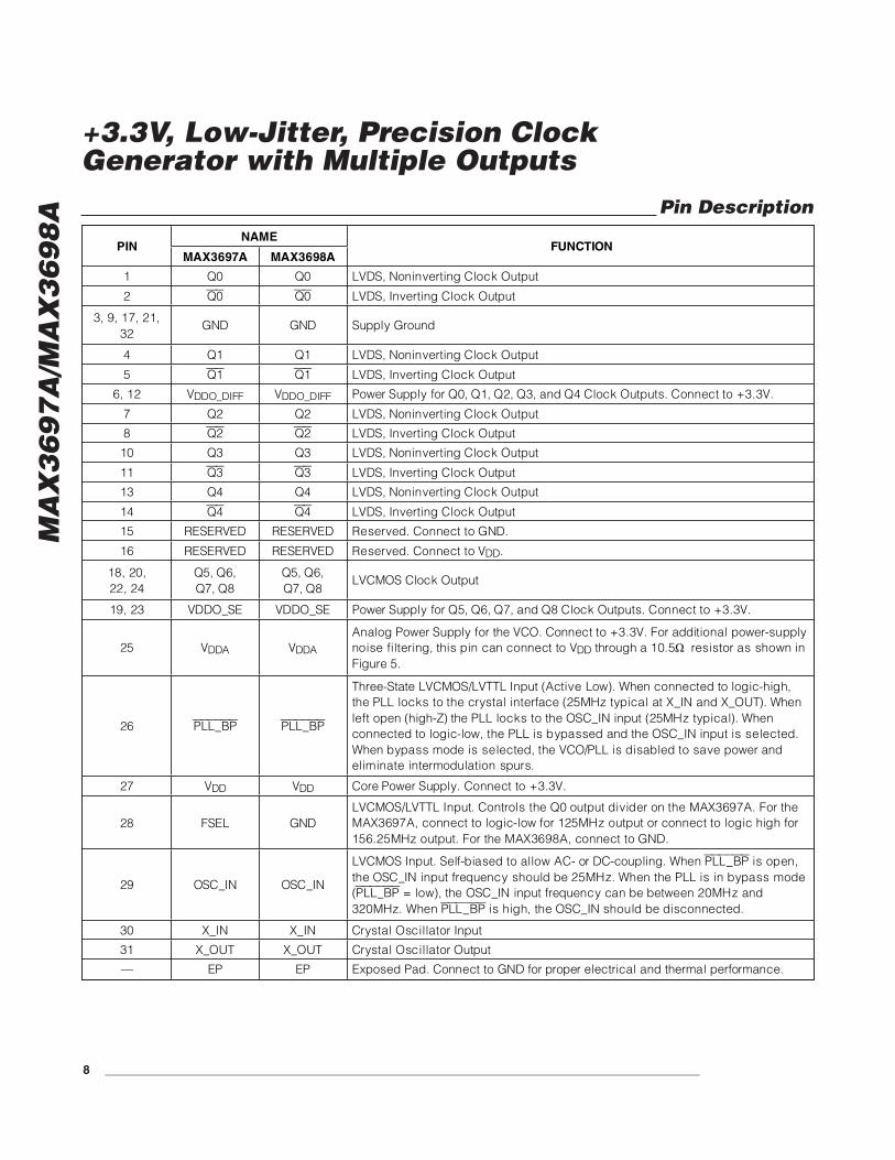
Pin DescriptionNAME
PINMAX3697A MAX3698A
FUNCTION
1 Q0 Q0 LVDS, Noninverting Clock Output
2 Q0 Q0 LVDS, Inverting Clock Output
3, 9, 17, 21, 32
GND GND Supply Ground
4 Q1 Q1 LVDS, Noninverting Clock Output
5 Q1 Q1 LVDS, Inverting Clock Output
6, 12 VDDO_DIFF VDDO_DIFF Power Supply for Q0, Q1, Q2, Q3, and Q4 Clock Outputs. Connect to +3.3V.
7 Q2 Q2 LVDS, Noninverting Clock Output
8 Q2 Q2 LVDS, Inverting Clock Output
10 Q3 Q3 LVDS, Noninverting Clock Output
11 Q3 Q3 LVDS, Inverting Clock Output
13 Q4 Q4 LVDS, Noninverting Clock Output
14 Q4 Q4 LVDS, Inverting Clock Output
15 RESERVED RESERVED Reserved. Connect to GND.
16 RESERVED RESERVED Reserved. Connect to VDD.
18, 20, 22, 24
Q5, Q6, Q7, Q8
Q5, Q6, Q7, Q8
LVCMOS Clock Output
19, 23 VDDO_SE VDDO_SE Power Supply for Q5, Q6, Q7, and Q8 Clock Outputs. Connect to +3.3V.
25 VDDA VDDA
Analog Power Supply for the VCO. Connect to +3.3V. For additional power-supply noise filtering, this pin can connect to VDD through a 10.5 resistor as shown in Figure 5.
26 PLL_BP PLL_BP
Three-State LVCMOS/LVTTL Input (Active Low). When connected to logic-high, the PLL locks to the crystal interface (25MHz typical at X_IN and X_OUT). When left open (high-Z) the PLL locks to the OSC_IN input (25MHz typical). When connected to logic-low, the PLL is bypassed and the OSC_IN input is selected. When bypass mode is selected, the VCO/PLL is disabled to save power and eliminate intermodulation spurs.
27 VDD VDD Core Power Supply. Connect to +3.3V.
28 FSEL GND LVCMOS/LVTTL Input. Controls the Q0 output divider on the MAX3697A. For the MAX3697A, connect to logic-low for 125MHz output or connect to logic high for 156.25MHz output. For the MAX3698A, connect to GND.
29 OSC_IN OSC_IN
LVCMOS Input. Self-biased to allow AC- or DC-coupling. When PLL_BP is open, the OSC_IN input frequency should be 25MHz. When the PLL is in bypass mode (PLL_BP = low), the OSC_IN input frequency can be between 20MHz and 320MHz. When PLL_BP is high, the OSC_IN should be disconnected.
30 X_IN X_IN Crystal Oscillator Input
31 X_OUT X_OUT Crystal Oscillator Output
— EP EP Exposed Pad. Connect to GND for proper electrical and thermal performance.

MA
X3
69
7A
/MA
X3
69
8A
+3.3V, Low-Jitter, Precision Clock Generator with Multiple Outputs
_______________________________________________________________________________________ 9
CRYSTALOSCILLATOR
OSC_IN
X_IN
X_OUT
0/OPEN
1
0
1/OPENPFD FILTER
DIVIDE25
DIVIDE5
DIVIDE32
VCO
PLL_BPLOGIC
125MHz
LVDSBUFFER
Q0
Q0
VDD VDDO_DIFF
VDDO_SE
PLL_BPVDDA
CMOS
LVDSBUFFER
Q1
Q1
LVDSBUFFER
Q2
Q2
LVDSBUFFER
Q3
Q3
LVDSBUFFER
Q4
Q4
LVCMOSBUFFER Q5125MHz
LVCMOSBUFFER Q6
LVCMOSBUFFER Q7
LVCMOSBUFFER Q8
3.90625MHz
MAX3698A
Figure 3. MAX3698A Functional Diagram
MA
X3
69
7A
/MA
X3
69
8A
+3.3V, Low-Jitter, Precision Clock Generator with Multiple Outputs
10 ______________________________________________________________________________________
CRYSTALOSCILLATOR
OSC_IN
X_IN
X_OUT
0/OPEN
1
0
1/OPENPFD FILTER
DIVIDE25
DIVIDE5 OR 4
DIVIDE5
DIVIDE32
VCO
PLL_BPLOGIC
125/156.25MHz
125MHz
LVDSBUFFER
Q0
Q0
VDD VDDO_DIFF
VDDO_SE
PLL_BPVDDA FSEL
CMOS
0
1/OPEN
125MHz
LVDSBUFFER
Q1
Q1
125MHz
LVDSBUFFER
Q2
Q2
125MHz
LVDSBUFFER
Q3
Q3
125MHz
LVDSBUFFER
Q4
Q4
LVCMOSBUFFER Q5
125MHz
125MHz
LVCMOSBUFFER Q6
LVCMOSBUFFER Q7
LVCMOSBUFFER Q8
3.90625MHz
MAX3697A
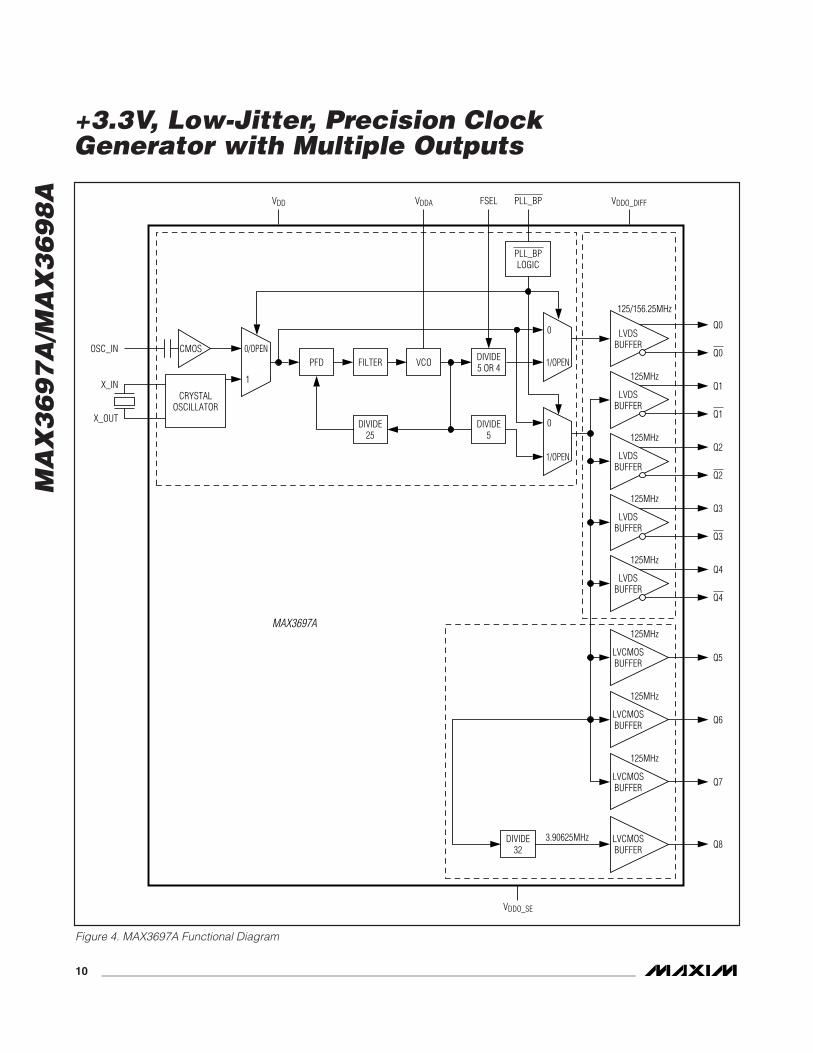
Figure 4. MAX3697A Functional Diagram

MA
X3
69
7A
/MA
X3
69
8A
+3.3V, Low-Jitter, Precision Clock Generator with Multiple Outputs
______________________________________________________________________________________ 11
Detailed DescriptionThe MAX3697A/MAX3698A are frequency generatorsdesigned to operate at Ethernet frequencies. They con-sist of an on-chip crystal oscillator, PLL, LVCMOS out-put buffers, and LVDS output buffers. Using alow-frequency clock (crystal or CMOS input) as a refer-ence, the internal PLL generates a high-frequency out-put clock with excellent j i tter performance. TheMAX3697A comes with a selector pin (FSEL) that allowsthe Q0 output to be switched between 125MHz and156.25MHz.
Crystal OscillatorAn integrated oscillator provides the low-frequency ref-erence clock for the PLL. This oscillator requires anexternal crystal connected between X_IN and X_OUT.The crystal frequency is 25MHz.
OSC_IN BufferThe LVCMOS OSC_IN buffer is internally biased toallow AC- or DC-coupling. This input is internally AC-coupled, and is designed to operate at 25MHz whenthe PLL is enabled (PLL_BP is left open). When the PLLis bypassed (PLL_BP is set low), the OSC_IN buffer canbe operated from 20MHz to 320MHz.
PLLThe PLL takes the signal from the crystal oscillator orreference clock input and synthesizes a low-jitter, high-frequency clock. The PLL contains a phase-frequencydetector (PFD), a lowpass filter, and a voltage-con-trolled oscillator (VCO) that operates at 625MHz. TheVCO output is connected to the PFD input through afeedback divider that divides the VCO frequency by 25to lock onto the 25MHz reference clock or oscillator.With the VCO locked onto the input reference, a stable125MHz output clock is provided through a final outputdivider. The MAX3697A includes an extra control pin(FSEL) that selects either 125MHz or 156.25MHz outputfrequency at Q0. To minimize noise-induced jitter, theVCO supply (VDDA) is isolated from the core logic andoutput buffer supplies.
LVDS DriversThe high-frequency outputs—Q0, Q1, Q2, Q3, and Q4—are differential LVDS buffers designed to drive 100Ω.
LVCMOS DriverLVCMOS outputs Q5, Q6, Q7, and Q8 are provided onthe MAX3697A/MAX3698A. They are designed to drivesingle-ended high-impedance loads. The maximumdata rate for Q5, Q6, and Q7 is 160MHz. Q8 output fre-quency is equal to the frequency of Q5, Q6, or Q7divided by 32.
Applications InformationPower-Supply Filtering
The MAX3697A/MAX3698A are mixed analog/digitalICs. The PLL contains analog circuitry susceptible torandom noise. To take full advantage of on-board filter-ing and noise attenuation, in addition to excellent on-chip power-supply rejection, these parts provide aseparate power-supply pin, VDDA, for the VCO circuitry.The purpose of this design technique is to ensure cleaninput power supply to the VCO circuitry and to improvethe overall immunity to power-supply noise. Figure 5illustrates the recommended power-supply filter net-work for VDDA. This network requires that the powersupply is +3.3V ±5%. Decoupling capacitors should beused on all other supply pins for best performance.
Crystal Input Layout and FrequencyStability
The MAX3697A/MAX3698A feature an integrated on-chip crystal oscillator to minimize system implementa-tion cost. The integrated crystal oscil lator is aPierce-type that uses the crystal in its parallel reso-nance mode. It is recommended to use a 25MHz crys-tal with a load specification of CL = 18pF. See Table 1for the recommended crystal specifications.
The crystal, trace, and two external capacitors shouldbe placed on the board as close as possible to theX_IN and X_OUT pins to reduce crosstalk and activesignals into the oscillator.
The layout shown in Figure 6 gives approximately 2pFof trace plus footprint capacitors per side of the crystal(Y1). The dielectric material is FR-4 and dielectric thick-ness of the reference board is 15 mils. Using a 25MHzcrystal and the capacitor values of C45 = 27pF andC46 = 33pF, the measured output frequency accuracyis -1ppm at +25°C ambient temperature.
VDD
VDDA
10.5Ω
+3.3V ±5%
0.01μF 10μF
0.1μF
Figure 5. Analog Supply Filtering

MA
X3
69
7A
/MA
X3
69
8A
+3.3V, Low-Jitter, Precision Clock Generator with Multiple Outputs
12 ______________________________________________________________________________________
Table 1. Crystal Selection Parameters
Crystal SelectionThe crystal oscillator is designed to drive a fundamentalmode, AT-cut crystal resonator. See Table 1 for recom-mended crystal specifications. See Figure 7 for externalcapacitance connection.
Figure 6. Crystal Layout
X_IN
X_OUT
27pF
33pF
CRYSTAL(CL = 18pF)
Figure 7. Crystal, Capacitors Connection
PARAMETER SYMBOL MIN TYP MAX UNITS
Crystal Oscillation Frequency fOSC 25 MHz
Shunt Capacitance CO 7.0 pF
Load Capacitance CL 18 pF
Equivalent Series Resistance (ESR) RS 50
Maximum Crystal Drive Level 300 μW

MA
X3
69
7A
/MA
X3
69
8A
+3.3V, Low-Jitter, Precision Clock Generator with Multiple Outputs
______________________________________________________________________________________ 13
Interface ModelsFigures 8 and 9 show examples of interface models.
Layout ConsiderationsThe inputs and outputs are the most critical paths forthe MAX3697A/MAX3698A and great care should betaken to minimize discontinuities on these transmissionlines between the connector and the IC. Here are somesuggestions for maximizing the performance of theMAX3697A/MAX3698A:
• An uninterrupted ground plane should be posi-tioned beneath the clock outputs. The ground
plane under the crystal should be removed to mini-mize capacitance.
• Ground pin vias should be placed close to the ICand the input/output interfaces to allow a returncurrent path to the MAX3697A/MAX3698A and thereceive devices.
• Supply decoupling capacitors should be placedclose to the supply pins, preferably on the samelayer as the MAX3697A/MAX3698A.
• Take care to isolate crystal input traces from theMAX3697A/MAX3698A outputs.
• The crystal, trace, and two external capacitorsshould be placed on the board as close as possi-ble to the X_IN and X_OUT pins to reducecrosstalk and active signals into the oscillator.
• Maintain 100Ω differential (or 50Ω single-ended)transmission line impedance into and out of thepart.
• Use good high-frequency layout techniques andmultilayer boards with an uninterrupted groundplane to minimize EMI and crosstalk.
Refer to the MAX3697A and MAX3698A evaluation kits formore information.
Exposed-Pad PackageThe exposed pad on the 32-pin TQFN package pro-vides a very low inductance path for return current trav-eling to the PCB ground plane. The pad is alsoelectrical ground on the MAX3697A/MAX3698A andmust be soldered to the circuit board ground for properelectrical performance.
Chip InformationTRANSISTOR COUNT: 13,768
PROCESS: BiCMOS
180kΩ
1.4V
ESDSTRUCTURES
OSC_IN
VDD
Figure 8. Simplified OSC_IN Pin Circuit Schematic
ROUT
ROUT
ESDSTRUCTURES
Q5 TO Q8
VDDO_SEVx
Vx = 2.7V FOR Q8Vx = VDDO_SE FOR Q5 TO Q7
ROUT = 50Ω FOR Q8ROUT = 10Ω FOR Q5 TO Q7
Figure 9. Simplified LVCMOS Output Circuit Schematic
PACKAGETYPE
PACKAGECODE
OUTLINENO.
LANDPATTERN
NO.
32 TQFN-EP T3255+5 21-0140 90-0013
Package InformationFor the latest package outline information and land patterns (footprints), go to . Note that a “+”, “#”, or “-” in the package code indicates RoHS status only. Package drawings may show a different suffix character, but the drawing pertains to the package regardless of RoHS status.
http://www.microsemi.com

MA
X3
69
7A
/MA
X3
69
8A
+3.3V, Low-Jitter, Precision Clock Generator with Multiple Outputs
Maxim cannot assume responsibility for use of any circuitry other than circuitry entirely embodied in a Maxim product. No circuit patent licenses areimplied. Maxim reserves the right to change the circuitry and specifications without notice at any time.
14 ____________________Maxim Integrated Products, 120 San Gabriel Drive, Sunnyvale, CA 94086 408-737-7600
© 2010 Maxim Integrated Products Maxim is a registered trademark of Maxim Integrated Products, Inc.
Revision HistoryREVISION NUMBER
REVISION DATE
DESCRIPTIONPAGES
CHANGED
0 8/10 Initial release —
� �14

Microsemi Corporate Headquarters One Enterprise, Aliso Viejo CA 92656 USA Within the USA: +1 (949) 380-6100 Sales: +1 (949) 380-6136 Fax: +1 (949) 215-4996
Microsemi Corporation (NASDAQ: MSCC) offers a comprehensive portfolio of semiconductor solutions for: aerospace, defense and security; enterprise and communications; and industrial and alternative energy markets. Products include high-performance, high-reliability analog and RF devices, mixed signal and RF integrated circuits, customizable SoCs, FPGAs, and complete subsystems. Microsemi is headquartered in Aliso Viejo, Calif. Learn more at www.microsemi.com.
© 2012 Microsemi Corporation. All rights reserved. Microsemi and the Microsemi logo are trademarks of Microsemi Corporation. All other trademarks and service marks are the property of their respective owners.