Embed Size (px)
Citation preview
Document Number: MC33911Rev. 4.0, 2/2008
Freescale Semiconductor Advance Information
LIN System Basis Chip with DC Motor Pre-driver
The 33911 is a Serial Peripheral Interface (SPI)-controlled System Basis Chip (SBC) combining many frequently used functions in an MCU-based system, plus a Local Interconnect Network (LIN) transceiver. The 33911 has a 5.0V - 60mA low dropout regulator with full protection and reporting features. The device provides full SPI-readable diagnostics and a selectable timing watchdog for detecting errant operation. The LIN Protocol Specification 2.0 compliant LIN transceiver, has waveshaping circuitry that can be disabled for higher data rates.
One 60mA high side switch and two 160mA low side switches with output protection are available for driving resistive and inductive loads. All outputs can be pulse-width modulated (PWM). Two high-voltage inputs are available for use in contact monitoring, or as external wake-up inputs. These inputs can be used as high-voltage analog Inputs. The voltage on theses pins is divided by a selectable ratio and available via an analog multiplexer.
The 33911 has three main operating modes: Normal (all functions available), Sleep (VDD off, wake-up via LIN, wake-up inputs (L1,L2), cyclic sense, and forced wake-up), and Stop (VDD on with limited current capability, wake-up via CS, LIN bus, wake-up inputs, cyclic sense, forced wake-up, and external reset).
The 33911 is compatible with LIN Protocol Specification 2.0.
Features• One 60mA high side switch and two 160mA low side switches• Two high-voltage analog/logic inputs• Full-duplex SPI Interface at frequencies up to 4MHz• LIN transceiver capable of up to 100kbps with wave shaping• Configurable window watchdog• 5.0V low drop regulator with fault detection and low-voltage reset (LVR) circuitry• Pb-free packaging designated by suffix code AC
Figure 1. 33911 Simplified Application Diagram
33911
ORDERING INFORMATION
Device Temperature Range (TA) Package
MC33911BAC/R2 - 40°C to 125°C32-LQFP
MC34911BAC/R2 - 40°C to 85°C
AC SUFFIX (Pb-FREE)98ASH70029A32-PIN LQFP
SYSTEM BASIS CHIP WITH LIN2ND GENERATION
M
MCU
33911VS1VS2
VSENSEHS1
L1L2
LS1
LS2
WDCONF
AGN
D
LGN
DP
GN
D
VDD
PWMINADOUT0
MOSIMISOSCLKCSRXDTXDIRQRST
VBAT
LIN INTERFACELIN
* This document contains certain information on a new product. Specifications and information herein are subject to change without notice.
© Freescale Semiconductor, Inc., 2007. All rights reserved.
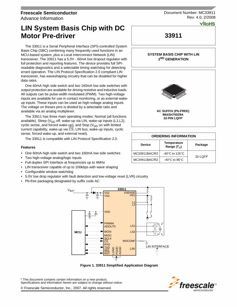
INTERNAL BLOCK DIAGRAM
33911
INTERNAL BLOCK DIAGRAM
Figure 2. 33911 Simplified Internal Block Diagram
VOLTAGE REGULATOR
HIGH SIDECONTROLMODULE
INTERRUPTCONTROLMODULE
LVI, HVI, HTI, OCI
RESET CONTROLMODULE
LVR, HVR, HTR, WD
WINDOWWATCHDOG
MODULE
SPI&
CONTROL
LIN PHYSICALLAYER
WAKE-UP MODULE
DIGITAL INPUT MODULE
ANALOG INPUT
CHIP TEMPERATURESENSE MODULE
AN
ALO
G M
ULT
IPLE
XE
R
MODULE
AGND
PGND
HS1
L1
LIN
RST IRQ VS2 VS1 VDD
PWMIN
MISO
MOSI
SCLK
CS
ADOUT0
RXD
TXD
LGND WDCONF
VS2
INTE
RN
AL
BU
SLOW SIDECONTROLMODULE
L2
VBATSENSE MODULE VSENSE
LS1
LS2
Analog Integrated Circuit Device Data 2 Freescale Semiconductor
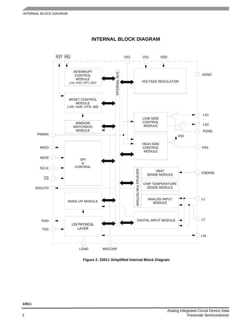
PIN CONNECTIONS
PIN CONNECTIONS
Figure 3. 33911 Pin Connections
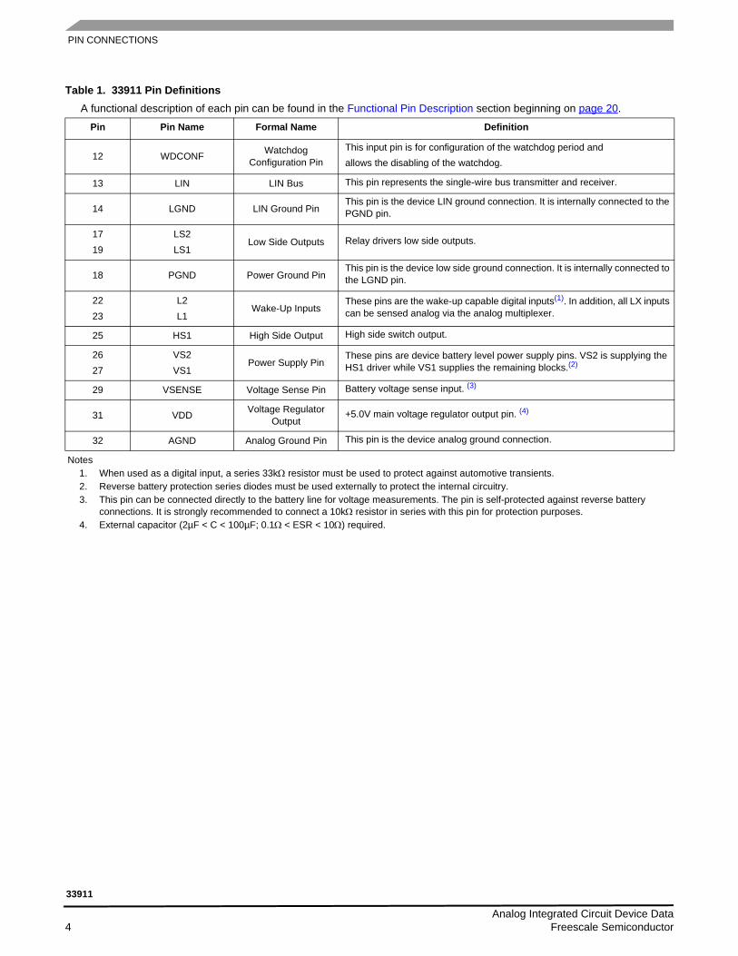
Table 1. 33911 Pin DefinitionsA functional description of each pin can be found in the Functional Pin Description section beginning on page 20.
Pin Pin Name Formal Name Definition
1 RXD Receiver OutputThis pin is the receiver output of the LIN interface which reports the state of the bus voltage to the MCU interface.
2 TXD Transmitter InputThis pin is the transmitter input of the LIN interface which controls the state of the bus output.
3 MISO SPI OutputSPI (Serial Peripheral Interface) data output. When CS is high, pin is in the high-impedance state.
4 MOSI SPI Input SPI (Serial Peripheral Interface) data input.
5 SCLK SPI Clock SPI (Serial Peripheral Interface) clock Input.
6 CS SPI Chip Select SPI (Serial Peripheral Interface) chip select input pin. CS is active low.
7 ADOUT0 Analog Output Pin 0 Analog Multiplexer Output.
8 PWMIN PWM Input High side and low side pulse-width modulation input.
9 RST Internal Reset I/OBidirectional reset I/O pin - driven low when any internal reset source is asserted. RST is active low.
10 IRQ Internal Interrupt Output
Interrupt output pin, indicating wake-up events from Stop Mode or events from Normal and Normal Request Modes. IRQ is active low.
8PWMIN
7ADOUT0
5SCLK
4MOSI
3MISO
1RXD
2TXD
6CS
17 LS2
18 PGND
20 NC*
21 NC*
22 L2
24 NC*
23 L1
19 LS1
25H
S1
26V
S2
28N
C
29V
SE
NS
E
30N
C*
32A
GN
D
31V
DD
27V
S1
16
NC
*
15
NC
*
13
LIN
12
WD
CO
NF
11
NC
*
9
RS
T
10
IRQ
14
LGN
D
* Special Configuration Recommended / Mandatory for Marked NC Pins
Analog Integrated Circuit Device Data Freescale Semiconductor 3
33911
PIN CONNECTIONS
12 WDCONF Watchdog Configuration Pin
This input pin is for configuration of the watchdog period andallows the disabling of the watchdog.
13 LIN LIN Bus This pin represents the single-wire bus transmitter and receiver.
14 LGND LIN Ground PinThis pin is the device LIN ground connection. It is internally connected to the PGND pin.
1719
LS2LS1
Low Side Outputs Relay drivers low side outputs.
18 PGND Power Ground PinThis pin is the device low side ground connection. It is internally connected to the LGND pin.
2223
L2L1
Wake-Up InputsThese pins are the wake-up capable digital inputs(1). In addition, all LX inputs can be sensed analog via the analog multiplexer.
25 HS1 High Side Output High side switch output.
2627
VS2VS1
Power Supply PinThese pins are device battery level power supply pins. VS2 is supplying the HS1 driver while VS1 supplies the remaining blocks.(2)
29 VSENSE Voltage Sense Pin Battery voltage sense input. (3)
31 VDD Voltage Regulator Output
+5.0V main voltage regulator output pin. (4)
32 AGND Analog Ground Pin This pin is the device analog ground connection.
Notes1. When used as a digital input, a series 33kΩ resistor must be used to protect against automotive transients.2. Reverse battery protection series diodes must be used externally to protect the internal circuitry.3. This pin can be connected directly to the battery line for voltage measurements. The pin is self-protected against reverse battery
connections. It is strongly recommended to connect a 10kΩ resistor in series with this pin for protection purposes.4. External capacitor (2µF < C < 100µF; 0.1Ω < ESR < 10Ω) required.
Table 1. 33911 Pin DefinitionsA functional description of each pin can be found in the Functional Pin Description section beginning on page 20.
Pin Pin Name Formal Name Definition
Analog Integrated Circuit Device Data 4 Freescale Semiconductor
33911
ELECTRICAL CHARACTERISTICSMAXIMUM RATINGS
ELECTRICAL CHARACTERISTICS
MAXIMUM RATINGS
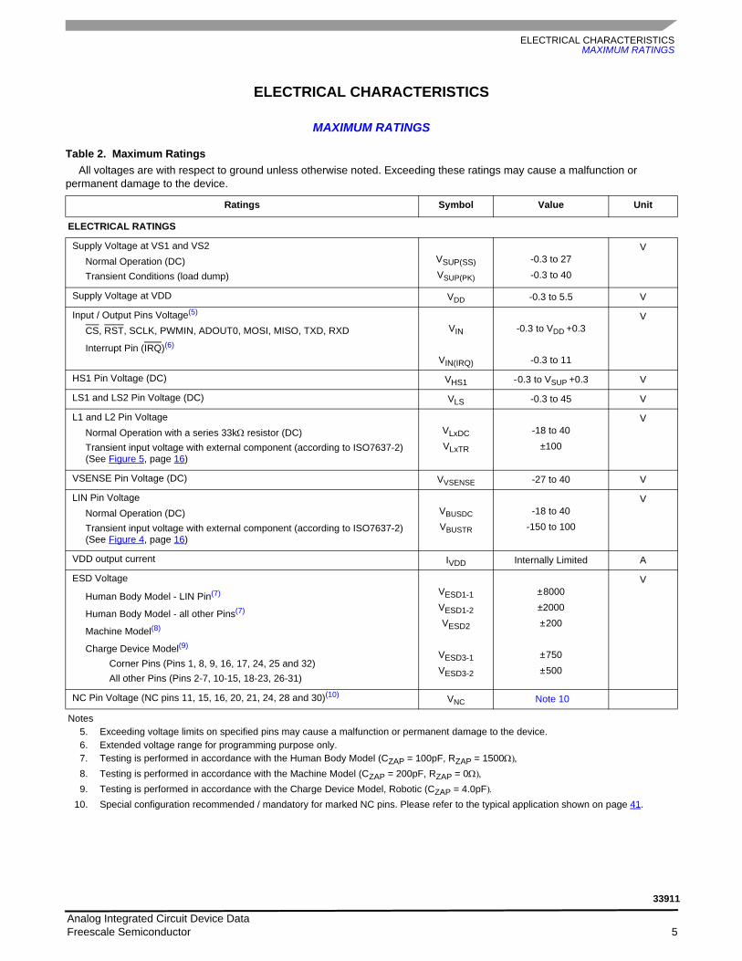
Table 2. Maximum Ratings All voltages are with respect to ground unless otherwise noted. Exceeding these ratings may cause a malfunction or
permanent damage to the device.
Ratings Symbol Value Unit
ELECTRICAL RATINGS
Supply Voltage at VS1 and VS2Normal Operation (DC)Transient Conditions (load dump)
VSUP(SS)VSUP(PK)
-0.3 to 27-0.3 to 40
V
Supply Voltage at VDD VDD -0.3 to 5.5 V
Input / Output Pins Voltage(5)
CS, RST, SCLK, PWMIN, ADOUT0, MOSI, MISO, TXD, RXD
Interrupt Pin (IRQ)(6)
VIN
VIN(IRQ)
-0.3 to VDD +0.3
-0.3 to 11
V
HS1 Pin Voltage (DC) VHS1 - 0.3 to VSUP +0.3 V
LS1 and LS2 Pin Voltage (DC) VLS -0.3 to 45 V
L1 and L2 Pin VoltageNormal Operation with a series 33kΩ resistor (DC)Transient input voltage with external component (according to ISO7637-2) (See Figure 5, page 16)
VLxDCVLxTR
-18 to 40±100
V
VSENSE Pin Voltage (DC) VVSENSE -27 to 40 V
LIN Pin VoltageNormal Operation (DC)Transient input voltage with external component (according to ISO7637-2) (See Figure 4, page 16)
VBUSDC
VBUSTR
-18 to 40-150 to 100
V
VDD output current IVDD Internally Limited A
ESD Voltage
Human Body Model - LIN Pin(7)
Human Body Model - all other Pins(7)
Machine Model(8)
Charge Device Model(9)
Corner Pins (Pins 1, 8, 9, 16, 17, 24, 25 and 32)All other Pins (Pins 2-7, 10-15, 18-23, 26-31)
VESD1-1VESD1-2VESD2
VESD3-1VESD3-2
± 8000±2000± 200
± 750± 500
V
NC Pin Voltage (NC pins 11, 15, 16, 20, 21, 24, 28 and 30)(10) VNC Note 10
Notes5. Exceeding voltage limits on specified pins may cause a malfunction or permanent damage to the device.6. Extended voltage range for programming purpose only.7. Testing is performed in accordance with the Human Body Model (CZAP = 100pF, RZAP = 1500Ω),
8. Testing is performed in accordance with the Machine Model (CZAP = 200pF, RZAP = 0Ω),
9. Testing is performed in accordance with the Charge Device Model, Robotic (CZAP = 4.0pF).
10. Special configuration recommended / mandatory for marked NC pins. Please refer to the typical application shown on page 41.
Analog Integrated Circuit Device Data Freescale Semiconductor 5
33911
ELECTRICAL CHARACTERISTICSMAXIMUM RATINGS
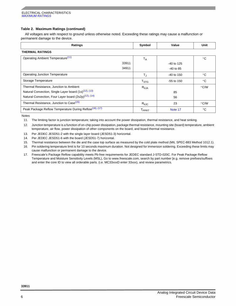
THERMAL RATINGS
Operating Ambient Temperature(11)
3391134911
TA-40 to 125-40 to 85
°C
Operating Junction Temperature TJ -40 to 150 °C
Storage Temperature TSTG -55 to 150 °C
Thermal Resistance, Junction to AmbientNatural Convection, Single Layer board (1s)(12), (13)
Natural Convection, Four Layer board (2s2p)(12), (14)
RθJA
8556
°C/W
Thermal Resistance, Junction to Case(15) RθJC 23 °C/W
Peak Package Reflow Temperature During Reflow(16), (17) TPPRT Note 17 °C
Notes11. The limiting factor is junction temperature; taking into account the power dissipation, thermal resistance, and heat sinking.12. Junction temperature is a function of on-chip power dissipation, package thermal resistance, mounting site (board) temperature, ambient
temperature, air flow, power dissipation of other components on the board, and board thermal resistance.13. Per JEDEC JESD51-2 with the single layer board (JESD51-3) horizontal.14. Per JEDEC JESD51-6 with the board (JESD51-7) horizontal.15. Thermal resistance between the die and the case top surface as measured by the cold plate method (MIL SPEC-883 Method 1012.1).16. Pin soldering temperature limit is for 10 seconds maximum duration. Not designed for immersion soldering. Exceeding these limits may
cause malfunction or permanent damage to the device.17. Freescale’s Package Reflow capability meets Pb-free requirements for JEDEC standard J-STD-020C. For Peak Package Reflow
Temperature and Moisture Sensitivity Levels (MSL), Go to www.freescale.com, search by part number [e.g. remove prefixes/suffixes and enter the core ID to view all orderable parts. (i.e. MC33xxxD enter 33xxx), and review parametrics.
Table 2. Maximum Ratings (continued)All voltages are with respect to ground unless otherwise noted. Exceeding these ratings may cause a malfunction or
permanent damage to the device.
Ratings Symbol Value Unit
Analog Integrated Circuit Device Data 6 Freescale Semiconductor
33911
ELECTRICAL CHARACTERISTICSSTATIC ELECTRICAL CHARACTERISTICS
STATIC ELECTRICAL CHARACTERISTICS
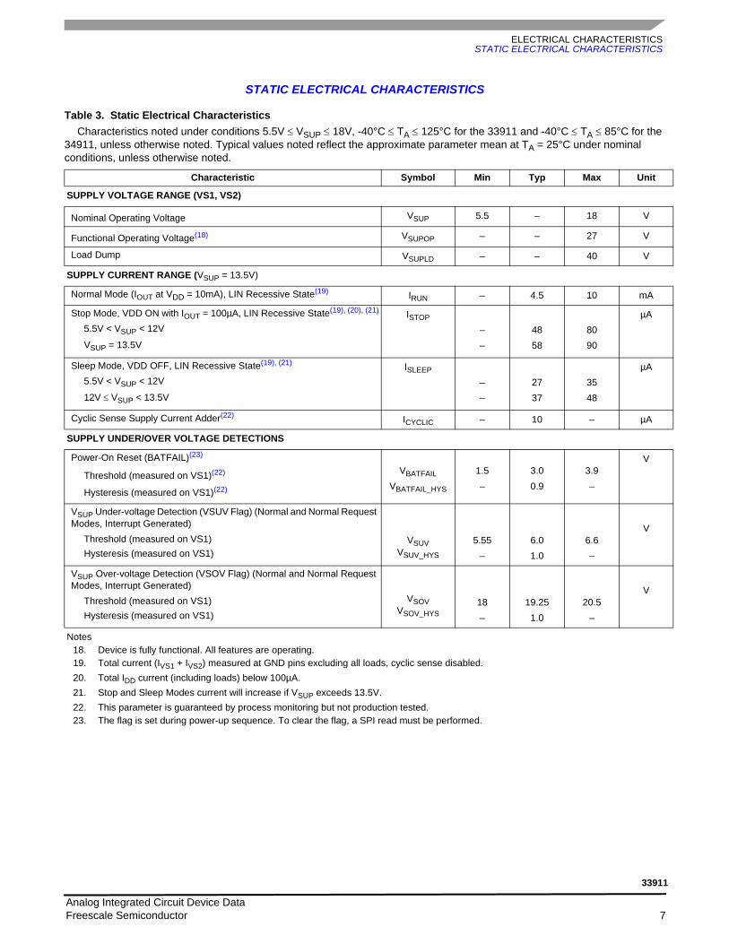
Table 3. Static Electrical Characteristics Characteristics noted under conditions 5.5V ≤ VSUP ≤ 18V, -40°C ≤ TA ≤ 125°C for the 33911 and -40°C ≤ TA ≤ 85°C for the
34911, unless otherwise noted. Typical values noted reflect the approximate parameter mean at TA = 25°C under nominal conditions, unless otherwise noted.
Characteristic Symbol Min Typ Max Unit
SUPPLY VOLTAGE RANGE (VS1, VS2)
Nominal Operating Voltage VSUP 5.5 – 18 V
Functional Operating Voltage(18) VSUPOP – – 27 V
Load Dump VSUPLD – – 40 V
SUPPLY CURRENT RANGE (VSUP = 13.5V)
Normal Mode (IOUT at VDD = 10mA), LIN Recessive State(19) IRUN – 4.5 10 mA
Stop Mode, VDD ON with IOUT = 100µA, LIN Recessive State(19), (20), (21)
5.5V < VSUP < 12V
VSUP = 13.5V
ISTOP
––
4858
8090
µA
Sleep Mode, VDD OFF, LIN Recessive State(19), (21)
5.5V < VSUP < 12V
12V ≤ VSUP < 13.5V
ISLEEP
––
2737
3548
µA
Cyclic Sense Supply Current Adder(22) ICYCLIC – 10 – µA
SUPPLY UNDER/OVER VOLTAGE DETECTIONS
Power-On Reset (BATFAIL)(23)
Threshold (measured on VS1)(22)
Hysteresis (measured on VS1)(22)
VBATFAIL
VBATFAIL_HYS
1.5–
3.00.9
3.9–
V
VSUP Under-voltage Detection (VSUV Flag) (Normal and Normal Request Modes, Interrupt Generated)
Threshold (measured on VS1)Hysteresis (measured on VS1)
VSUVVSUV_HYS
5.55–
6.01.0
6.6–
V
VSUP Over-voltage Detection (VSOV Flag) (Normal and Normal Request Modes, Interrupt Generated)
Threshold (measured on VS1)Hysteresis (measured on VS1)
VSOVVSOV_HYS
18–
19.251.0
20.5–
V
Notes18. Device is fully functional. All features are operating.19. Total current (IVS1 + IVS2) measured at GND pins excluding all loads, cyclic sense disabled.20. Total IDD current (including loads) below 100µA.21. Stop and Sleep Modes current will increase if VSUP exceeds 13.5V.22. This parameter is guaranteed by process monitoring but not production tested. 23. The flag is set during power-up sequence. To clear the flag, a SPI read must be performed.
Analog Integrated Circuit Device Data Freescale Semiconductor 7
33911
ELECTRICAL CHARACTERISTICSSTATIC ELECTRICAL CHARACTERISTICS
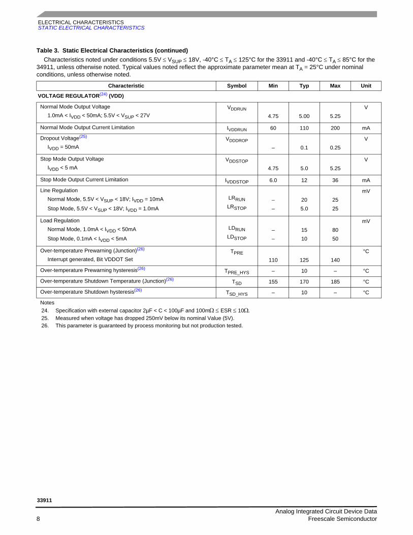
VOLTAGE REGULATOR(24) (VDD)
Normal Mode Output Voltage1.0mA < IVDD < 50mA; 5.5V < VSUP < 27V
VDDRUN
4.75 5.00 5.25V
Normal Mode Output Current Limitation IVDDRUN 60 110 200 mA
Dropout Voltage(25)
IVDD = 50mAVDDDROP
– 0.1 0.25V
Stop Mode Output VoltageIVDD < 5 mA
VDDSTOP4.75 5.0 5.25
V
Stop Mode Output Current Limitation IVDDSTOP 6.0 12 36 mA
Line RegulationNormal Mode, 5.5V < VSUP < 18V; IVDD = 10mA
Stop Mode, 5.5V < VSUP < 18V; IVDD = 1.0mA
LRRUNLRSTOP
––
205.0
2525
mV
Load RegulationNormal Mode, 1.0mA < IVDD < 50mA
Stop Mode, 0.1mA < IVDD < 5mA
LDRUNLDSTOP
––
1510
8050
mV
Over-temperature Prewarning (Junction)(26)
Interrupt generated, Bit VDDOT SetTPRE
110 125 140°C
Over-temperature Prewarning hysteresis(26) TPRE_HYS – 10 – °C
Over-temperature Shutdown Temperature (Junction)(26) TSD 155 170 185 °C
Over-temperature Shutdown hysteresis(26) TSD_HYS – 10 – °C
Notes24. Specification with external capacitor 2µF < C < 100µF and 100mΩ ≤ ESR ≤ 10Ω.25. Measured when voltage has dropped 250mV below its nominal Value (5V).26. This parameter is guaranteed by process monitoring but not production tested.
Table 3. Static Electrical Characteristics (continued)Characteristics noted under conditions 5.5V ≤ VSUP ≤ 18V, -40°C ≤ TA ≤ 125°C for the 33911 and -40°C ≤ TA ≤ 85°C for the
34911, unless otherwise noted. Typical values noted reflect the approximate parameter mean at TA = 25°C under nominal conditions, unless otherwise noted.
Characteristic Symbol Min Typ Max Unit
Analog Integrated Circuit Device Data 8 Freescale Semiconductor
33911
ELECTRICAL CHARACTERISTICSSTATIC ELECTRICAL CHARACTERISTICS
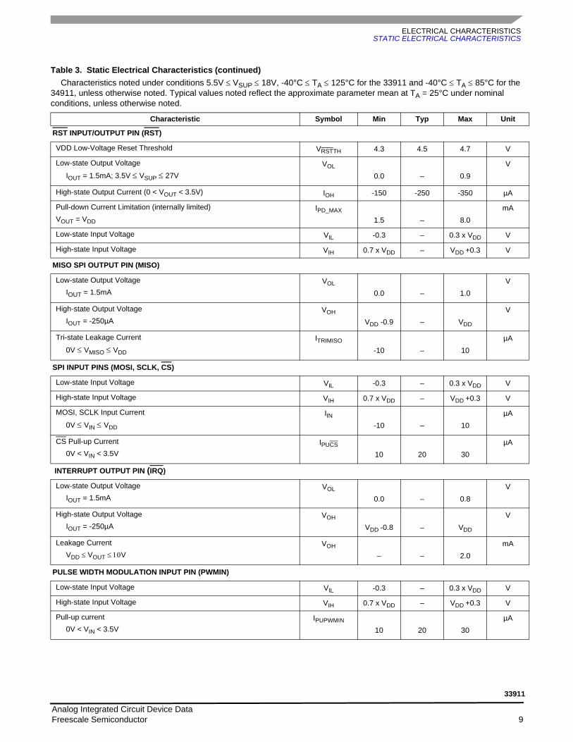
RST INPUT/OUTPUT PIN (RST)
VDD Low-Voltage Reset Threshold VRSTTH 4.3 4.5 4.7 V
Low-state Output Voltage
IOUT = 1.5mA; 3.5V ≤ VSUP ≤ 27VVOL
0.0 – 0.9V
High-state Output Current (0 < VOUT < 3.5V) IOH -150 -250 -350 µA
Pull-down Current Limitation (internally limited)VOUT = VDD
IPD_MAX
1.5 – 8.0mA
Low-state Input Voltage VIL -0.3 – 0.3 x VDD V
High-state Input Voltage VIH 0.7 x VDD – VDD +0.3 V
MISO SPI OUTPUT PIN (MISO)
Low-state Output Voltage IOUT = 1.5mA
VOL
0.0 – 1.0V
High-state Output VoltageIOUT = -250µA
VOH
VDD -0.9 – VDD
V
Tri-state Leakage Current
0V ≤ VMISO ≤ VDD
ITRIMISO
-10 – 10µA
SPI INPUT PINS (MOSI, SCLK, CS)
Low-state Input Voltage VIL -0.3 – 0.3 x VDD V
High-state Input Voltage VIH 0.7 x VDD – VDD +0.3 V
MOSI, SCLK Input Current
0V ≤ VIN ≤ VDD
IIN-10 – 10
µA
CS Pull-up Current0V < VIN < 3.5V
IPUCS
10 20 30µA
INTERRUPT OUTPUT PIN (IRQ)
Low-state Output VoltageIOUT = 1.5mA
VOL
0.0 – 0.8V
High-state Output VoltageIOUT = -250µA
VOH
VDD -0.8 – VDD
V
Leakage CurrentVDD ≤ VOUT ≤ 10V
VOH
– – 2.0mA
PULSE WIDTH MODULATION INPUT PIN (PWMIN)
Low-state Input Voltage VIL -0.3 – 0.3 x VDD V
High-state Input Voltage VIH 0.7 x VDD – VDD +0.3 V
Pull-up current0V < VIN < 3.5V
IPUPWMIN
10 20 30µA
Table 3. Static Electrical Characteristics (continued)Characteristics noted under conditions 5.5V ≤ VSUP ≤ 18V, -40°C ≤ TA ≤ 125°C for the 33911 and -40°C ≤ TA ≤ 85°C for the
34911, unless otherwise noted. Typical values noted reflect the approximate parameter mean at TA = 25°C under nominal conditions, unless otherwise noted.
Characteristic Symbol Min Typ Max Unit
Analog Integrated Circuit Device Data Freescale Semiconductor 9
33911
ELECTRICAL CHARACTERISTICSSTATIC ELECTRICAL CHARACTERISTICS
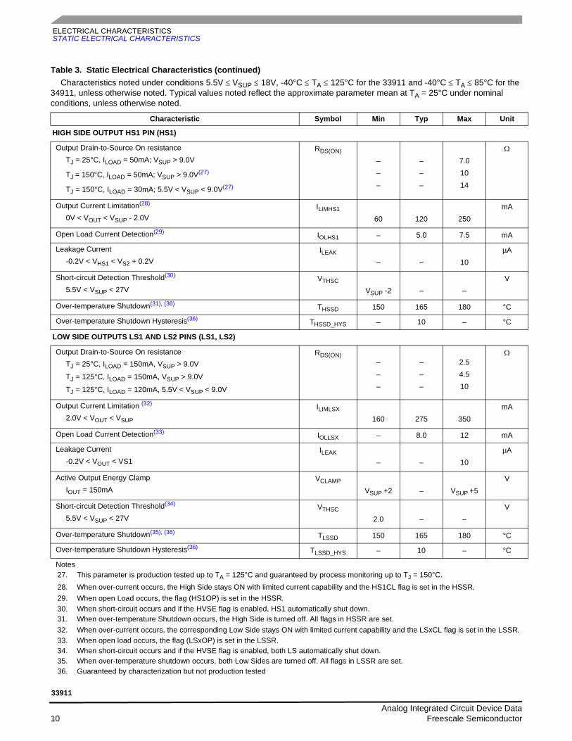
HIGH SIDE OUTPUT HS1 PIN (HS1)
Output Drain-to-Source On resistanceTJ = 25°C, ILOAD = 50mA; VSUP > 9.0V
TJ = 150°C, ILOAD = 50mA; VSUP > 9.0V(27)
TJ = 150°C, ILOAD = 30mA; 5.5V < VSUP < 9.0V(27)
RDS(ON)
–––
–––
7.01014
Ω
Output Current Limitation(28)
0V < VOUT < VSUP - 2.0VILIMHS1
60 120 250mA
Open Load Current Detection(29) IOLHS1 – 5.0 7.5 mA
Leakage Current -0.2V < VHS1 < VS2 + 0.2V
ILEAK
– – 10µA
Short-circuit Detection Threshold(30)
5.5V < VSUP < 27VVTHSC
VSUP -2 – –V
Over-temperature Shutdown(31), (36) THSSD 150 165 180 °C
Over-temperature Shutdown Hysteresis(36) THSSD_HYS – 10 – °C
LOW SIDE OUTPUTS LS1 AND LS2 PINS (LS1, LS2)
Output Drain-to-Source On resistanceTJ = 25°C, ILOAD = 150mA, VSUP > 9.0V
TJ = 125°C, ILOAD = 150mA, VSUP > 9.0V
TJ = 125°C, ILOAD = 120mA, 5.5V < VSUP < 9.0V
RDS(ON)–––
–––
2.54.510
Ω
Output Current Limitation (32)
2.0V < VOUT < VSUP
ILIMLSX
160 275 350mA
Open Load Current Detection(33) IOLLSX – 8.0 12 mA
Leakage Current-0.2V < VOUT < VS1
ILEAK
– – 10µA
Active Output Energy ClampIOUT = 150mA
VCLAMP
VSUP +2 – VSUP +5V
Short-circuit Detection Threshold(34)
5.5V < VSUP < 27VVTHSC
2.0 – –V
Over-temperature Shutdown(35), (36) TLSSD 150 165 180 °C
Over-temperature Shutdown Hysteresis(36) TLSSD_HYS – 10 – °C
Notes27. This parameter is production tested up to TA = 125°C and guaranteed by process monitoring up to TJ = 150°C.28. When over-current occurs, the High Side stays ON with limited current capability and the HS1CL flag is set in the HSSR.29. When open Load occurs, the flag (HS1OP) is set in the HSSR.30. When short-circuit occurs and if the HVSE flag is enabled, HS1 automatically shut down.31. When over-temperature Shutdown occurs, the High Side is turned off. All flags in HSSR are set.32. When over-current occurs, the corresponding Low Side stays ON with limited current capability and the LSxCL flag is set in the LSSR.33. When open load occurs, the flag (LSxOP) is set in the LSSR.34. When short-circuit occurs and if the HVSE flag is enabled, both LS automatically shut down.35. When over-temperature shutdown occurs, both Low Sides are turned off. All flags in LSSR are set.36. Guaranteed by characterization but not production tested
Table 3. Static Electrical Characteristics (continued)Characteristics noted under conditions 5.5V ≤ VSUP ≤ 18V, -40°C ≤ TA ≤ 125°C for the 33911 and -40°C ≤ TA ≤ 85°C for the
34911, unless otherwise noted. Typical values noted reflect the approximate parameter mean at TA = 25°C under nominal conditions, unless otherwise noted.
Characteristic Symbol Min Typ Max Unit
Analog Integrated Circuit Device Data 10 Freescale Semiconductor
33911
ELECTRICAL CHARACTERISTICSSTATIC ELECTRICAL CHARACTERISTICS
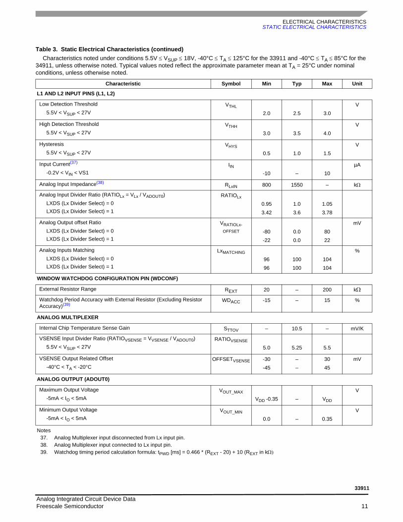
L1 AND L2 INPUT PINS (L1, L2)
Low Detection Threshold5.5V < VSUP < 27V
VTHL
2.0 2.5 3.0V
High Detection Threshold5.5V < VSUP < 27V
VTHH
3.0 3.5 4.0V
Hysteresis5.5V < VSUP < 27V
VHYS
0.5 1.0 1.5V
Input Current(37)
-0.2V < VIN < VS1IIN
-10 – 10µA
Analog Input Impedance(38) RLxIN 800 1550 – kΩ
Analog Input Divider Ratio (RATIOLx = VLx / VADOUT0)LXDS (Lx Divider Select) = 0LXDS (Lx Divider Select) = 1
RATIOLx
0.953.42
1.03.6
1.053.78
Analog Output offset RatioLXDS (Lx Divider Select) = 0LXDS (Lx Divider Select) = 1
VRATIOLx-OFFSET -80
-220.00.0
8022
mV
Analog Inputs MatchingLXDS (Lx Divider Select) = 0LXDS (Lx Divider Select) = 1
LxMATCHING
9696
100100
104104
%
WINDOW WATCHDOG CONFIGURATION PIN (WDCONF)
External Resistor Range REXT 20 – 200 kΩ
Watchdog Period Accuracy with External Resistor (Excluding Resistor Accuracy)(39)
WDACC -15 – 15 %
ANALOG MULTIPLEXER
Internal Chip Temperature Sense Gain STTOV – 10.5 – mV/K
VSENSE Input Divider Ratio (RATIOVSENSE = VVSENSE / VADOUT0)5.5V < VSUP < 27V
RATIOVSENSE
5.0 5.25 5.5
VSENSE Output Related Offset-40°C < TA < -20°C
OFFSETVSENSE -30-45
––
3045
mV
ANALOG OUTPUT (ADOUT0)
Maximum Output Voltage-5mA < IO < 5mA
VOUT_MAX
VDD -0.35 – VDD
V
Minimum Output Voltage-5mA < IO < 5mA
VOUT_MIN
0.0 – 0.35V
Notes37. Analog Multiplexer input disconnected from Lx input pin.38. Analog Multiplexer input connected to Lx input pin.39. Watchdog timing period calculation formula: tPWD [ms] = 0.466 * (REXT - 20) + 10 (REXT in kΩ)
Table 3. Static Electrical Characteristics (continued)Characteristics noted under conditions 5.5V ≤ VSUP ≤ 18V, -40°C ≤ TA ≤ 125°C for the 33911 and -40°C ≤ TA ≤ 85°C for the
34911, unless otherwise noted. Typical values noted reflect the approximate parameter mean at TA = 25°C under nominal conditions, unless otherwise noted.
Characteristic Symbol Min Typ Max Unit
Analog Integrated Circuit Device Data Freescale Semiconductor 11
33911
ELECTRICAL CHARACTERISTICSSTATIC ELECTRICAL CHARACTERISTICS
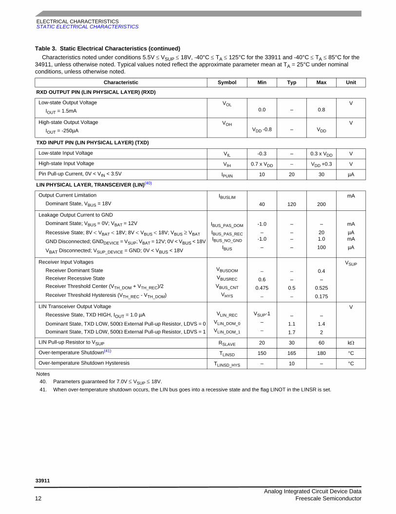
RXD OUTPUT PIN (LIN PHYSICAL LAYER) (RXD)
Low-state Output Voltage IOUT = 1.5mA
VOL0.0 – 0.8
V
High-state Output VoltageIOUT = -250µA
VOHVDD -0.8 – VDD
V
TXD INPUT PIN (LIN PHYSICAL LAYER) (TXD)
Low-state Input Voltage VIL -0.3 – 0.3 x VDD V
High-state Input Voltage VIH 0.7 x VDD – VDD +0.3 V
Pin Pull-up Current, 0V < VIN < 3.5V IPUIN 10 20 30 µA
LIN PHYSICAL LAYER, TRANSCEIVER (LIN)(40)
Output Current Limitation Dominant State, VBUS = 18V
IBUSLIM
40 120 200mA
Leakage Output Current to GNDDominant State; VBUS = 0V; VBAT = 12V
Recessive State; 8V < VBAT < 18V; 8V < VBUS < 18V; VBUS ≥ VBAT
GND Disconnected; GNDDEVICE = VSUP; VBAT = 12V; 0V < VBUS < 18V
VBAT Disconnected; VSUP_DEVICE = GND; 0V < VBUS < 18V
IBUS_PAS_DOM
IBUS_PAS_RECIBUS_NO_GND
IBUS
-1.0–
-1.0–
––––
–201.0100
mAµAmAµA
Receiver Input VoltagesReceiver Dominant StateReceiver Recessive StateReceiver Threshold Center (VTH_DOM + VTH_REC)/2
Receiver Threshold Hysteresis (VTH_REC - VTH_DOM)
VBUSDOM
VBUSREC
VBUS_CNT
VHYS
–0.6
0.475–
––
0.5–
0.4–
0.5250.175
VSUP
LIN Transceiver Output VoltageRecessive State, TXD HIGH, IOUT = 1.0 µA
Dominant State, TXD LOW, 500Ω External Pull-up Resistor, LDVS = 0Dominant State, TXD LOW, 500Ω External Pull-up Resistor, LDVS = 1
VLIN_REC
VLIN_DOM_0
VLIN_DOM_1
VSUP-1––
–1.11.7
–1.42
V
LIN Pull-up Resistor to VSUP RSLAVE 20 30 60 kΩ
Over-temperature Shutdown(41) TLINSD 150 165 180 °C
Over-temperature Shutdown Hysteresis TLINSD_HYS – 10 – °C
Notes40. Parameters guaranteed for 7.0V ≤ VSUP ≤ 18V. 41. When over-temperature shutdown occurs, the LIN bus goes into a recessive state and the flag LINOT in the LINSR is set.
Table 3. Static Electrical Characteristics (continued)Characteristics noted under conditions 5.5V ≤ VSUP ≤ 18V, -40°C ≤ TA ≤ 125°C for the 33911 and -40°C ≤ TA ≤ 85°C for the
34911, unless otherwise noted. Typical values noted reflect the approximate parameter mean at TA = 25°C under nominal conditions, unless otherwise noted.
Characteristic Symbol Min Typ Max Unit
Analog Integrated Circuit Device Data 12 Freescale Semiconductor
33911
ELECTRICAL CHARACTERISTICSDYNAMIC ELECTRICAL CHARACTERISTICS
DYNAMIC ELECTRICAL CHARACTERISTICS
Table 4. Dynamic Electrical Characteristics
Characteristics noted under conditions 5.5V ≤ VSUP ≤ 18V, -40°C ≤ TA ≤ 125°C for the 33911 and -40°C ≤ TA ≤ 85°C for the 34911, otherwise noted. Typical values noted reflect the approximate parameter mean at TA = 25°C under nominal conditions, unless otherwise noted.
Characteristic Symbol Min Typ Max Unit
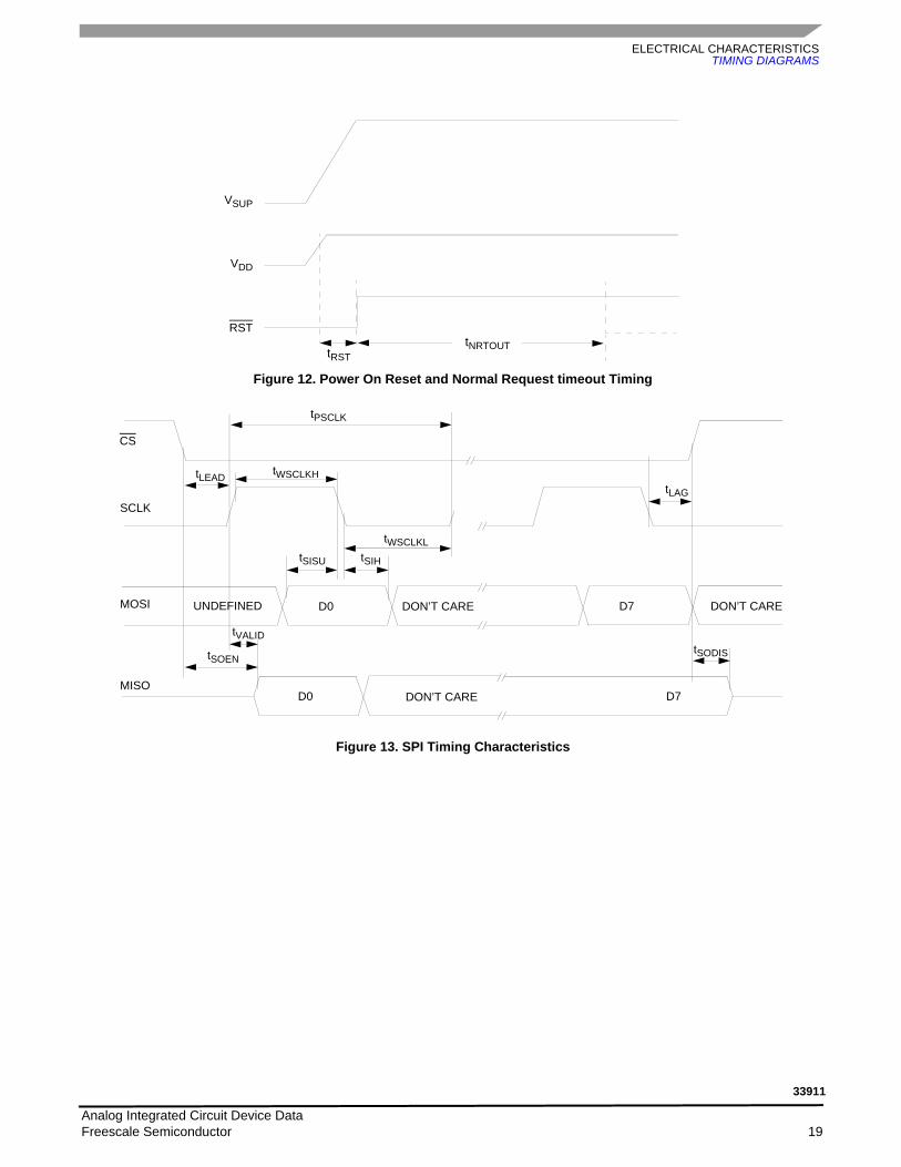
SPI INTERFACE TIMING (see Figure 13, page 19)
SPI Operating Frequency f SPIOP – – 4.0 MHz
SCLK Clock Period tPSCLK 250 – N/A ns
SCLK Clock High Time(42) tWSCLKH 110 – N/A ns
SCLK Clock Low Time(42) tWSCLKL 110 – N/A ns
Falling Edge of CS to Rising Edge of SCLK(42) tLEAD 100 – N/A ns
Falling Edge of SCLK to CS Rising Edge(42) tLAG 100 – N/A ns
MOSI to Falling Edge of SCLK(42) tSISU 40 – N/A ns
Falling Edge of SCLK to MOSI(42) tSIH 40 – N/A ns
MISO Rise Time(42)
CL = 220pFtRSO
– 40 –ns
MISO Fall Time(42)
CL = 220pFtFSO
– 40 –ns
Time from Falling or Rising Edges of CS to:(42)
- MISO Low-impedance- MISO High -impedance
tSOENtSODIS
0.00.0
––
5050
ns
Time from Rising Edge of SCLK to MISO Data Valid(42)
0.2 x VDD ≤ MISO ≥ 0.8 x VDD, CL = 100pFtVALID
0.0 – 75ns
RST OUTPUT PIN
Reset Low-Level Duration after VDD High (see Figure 12, page 19) t RST 0.65 1.0 1.35 ms
Reset Deglitch Filter Time t RSTDF 350 600 900 ns
WINDOW WATCHDOG CONFIGURATION PIN (WDCONF)
Watchdog Time Period (43)
External Resistor REXT = 20kΩ (1%)
External Resistor REXT = 200kΩ (1%)
Without External Resistor REXT (WDCONF pin open)
t PWD8.579
110
1094
150
11.5108205
ms
Notes42. This parameter is guaranteed by process monitoring but not production tested.43. Watchdog timing period calculation formula: tPWD [ms] = 0.466 * (REXT - 20) + 10 (REXT in kΩ)
Analog Integrated Circuit Device Data Freescale Semiconductor 13
33911
ELECTRICAL CHARACTERISTICSDYNAMIC ELECTRICAL CHARACTERISTICS
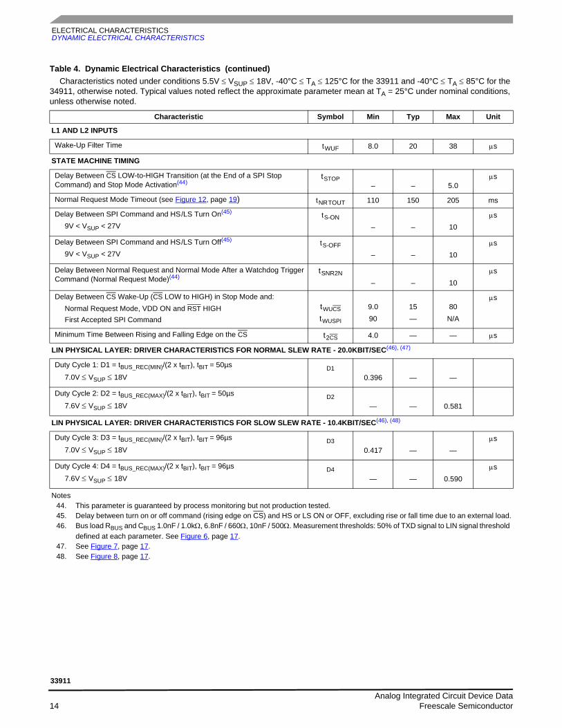
L1 AND L2 INPUTS
Wake-Up Filter Time t WUF 8.0 20 38 µs
STATE MACHINE TIMING
Delay Between CS LOW-to-HIGH Transition (at the End of a SPI Stop Command) and Stop Mode Activation(44)
t STOP– – 5.0
µs
Normal Request Mode Timeout (see Figure 12, page 19) t NR TOUT 110 150 205 ms
Delay Between SPI Command and HS /LS Turn On(45)
9V < VSUP < 27Vt S-ON
– – 10µs
Delay Between SPI Command and HS /LS Turn Off(45)
9V < VSUP < 27Vt S-OFF
– – 10µs
Delay Between Normal Request and Normal Mode After a Watchdog Trigger Command (Normal Request Mode)(44)
t SNR2N– – 10
µs
Delay Between CS Wake-Up (CS LOW to HIGH) in Stop Mode and:Normal Request Mode, VDD ON and RST HIGHFirst Accepted SPI Command
t WUCS
t WUSPI
9.090
15—
80N/A
µs
Minimum Time Between Rising and Falling Edge on the CS t 2CS 4.0 — — µs
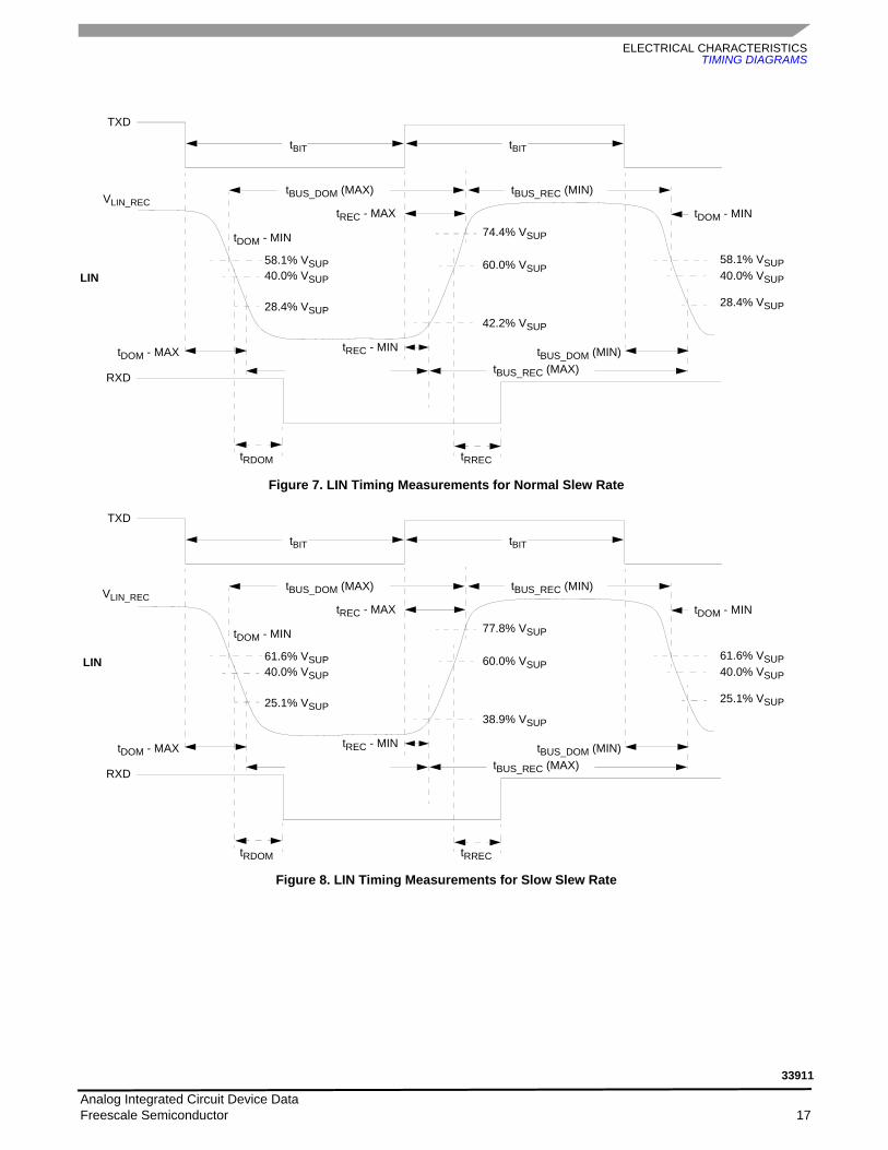
LIN PHYSICAL LAYER: DRIVER CHARACTERISTICS FOR NORMAL SLEW RATE - 20.0KBIT/SEC(46), (47)
Duty Cycle 1: D1 = tBUS_REC(MIN)/(2 x tBIT), tBIT = 50µs
7.0V ≤ VSUP ≤ 18VD1
0.396 — —
Duty Cycle 2: D2 = tBUS_REC(MAX)/(2 x tBIT), tBIT = 50µs
7.6V ≤ VSUP ≤ 18VD2
— — 0.581
LIN PHYSICAL LAYER: DRIVER CHARACTERISTICS FOR SLOW SLEW RATE - 10.4KBIT/SEC(46), (48)
Duty Cycle 3: D3 = tBUS_REC(MIN)/(2 x tBIT), tBIT = 96µs
7.0V ≤ VSUP ≤ 18VD3
0.417 — —µs
Duty Cycle 4: D4 = tBUS_REC(MAX)/(2 x tBIT), tBIT = 96µs
7.6V ≤ VSUP ≤ 18VD4
— — 0.590µs
Notes44. This parameter is guaranteed by process monitoring but not production tested.45. Delay between turn on or off command (rising edge on CS) and HS or LS ON or OFF, excluding rise or fall time due to an external load.46. Bus load RBUS and CBUS 1.0nF / 1.0kΩ, 6.8nF / 660Ω, 10nF / 500Ω. Measurement thresholds: 50% of TXD signal to LIN signal threshold
defined at each parameter. See Figure 6, page 17.47. See Figure 7, page 17.48. See Figure 8, page 17.
Table 4. Dynamic Electrical Characteristics (continued)Characteristics noted under conditions 5.5V ≤ VSUP ≤ 18V, -40°C ≤ TA ≤ 125°C for the 33911 and -40°C ≤ TA ≤ 85°C for the
34911, otherwise noted. Typical values noted reflect the approximate parameter mean at TA = 25°C under nominal conditions, unless otherwise noted.
Characteristic Symbol Min Typ Max Unit
Analog Integrated Circuit Device Data 14 Freescale Semiconductor
33911
ELECTRICAL CHARACTERISTICSDYNAMIC ELECTRICAL CHARACTERISTICS
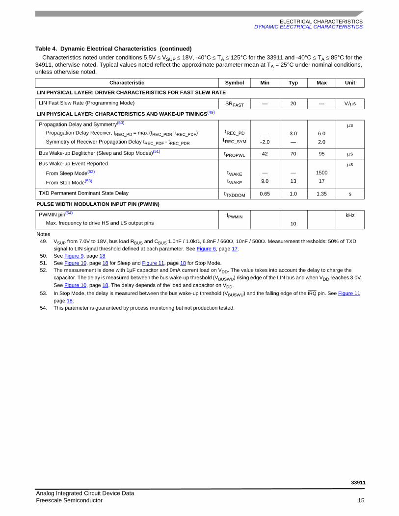
LIN PHYSICAL LAYER: DRIVER CHARACTERISTICS FOR FAST SLEW RATE
LIN Fast Slew Rate (Programming Mode) SRFAST — 20 — V / µs
LIN PHYSICAL LAYER: CHARACTERISTICS AND WAKE-UP TIMINGS(49)
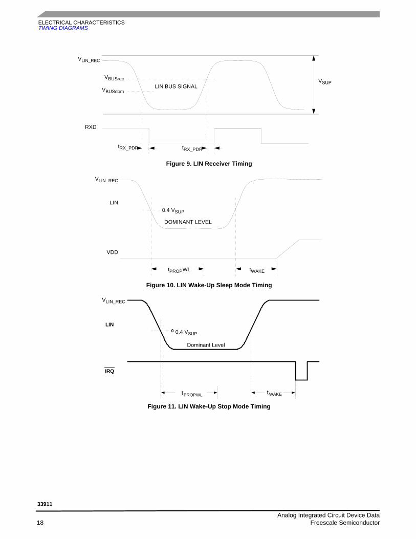
Propagation Delay and Symmetry(50)
Propagation Delay Receiver, tREC_PD = max (tREC_PDR, tREC_PDF)
Symmetry of Receiver Propagation Delay tREC_PDF - tREC_PDR
t REC_PDt REC_SYM
—- 2.0
3.0—
6.02.0
µs
Bus Wake-up Deglitcher (Sleep and Stop Modes)(51) t PROPWL 42 70 95 µs
Bus Wake-up Event Reported
From Sleep Mode(52)
From Stop Mode(53)
t WAKEt WAKE
—9.0
—13
150017
µs
TXD Permanent Dominant State Delay t TXDDOM 0.65 1.0 1.35 s
PULSE WIDTH MODULATION INPUT PIN (PWMIN)
PWMIN pin(54)
Max. frequency to drive HS and LS output pinsfPWMIN
10kHz
Notes49. VSUP from 7.0V to 18V, bus load RBUS and CBUS 1.0nF / 1.0kΩ, 6.8nF / 660Ω, 10nF / 500Ω. Measurement thresholds: 50% of TXD
signal to LIN signal threshold defined at each parameter. See Figure 6, page 17.50. See Figure 9, page 1851. See Figure 10, page 18 for Sleep and Figure 11, page 18 for Stop Mode.52. The measurement is done with 1µF capacitor and 0mA current load on VDD. The value takes into account the delay to charge the
capacitor. The delay is measured between the bus wake-up threshold (VBUSWU) rising edge of the LIN bus and when VDD reaches 3.0V. See Figure 10, page 18. The delay depends of the load and capacitor on VDD.
53. In Stop Mode, the delay is measured between the bus wake-up threshold (VBUSWU) and the falling edge of the IRQ pin. See Figure 11, page 18.
54. This parameter is guaranteed by process monitoring but not production tested.
Table 4. Dynamic Electrical Characteristics (continued)Characteristics noted under conditions 5.5V ≤ VSUP ≤ 18V, -40°C ≤ TA ≤ 125°C for the 33911 and -40°C ≤ TA ≤ 85°C for the
34911, otherwise noted. Typical values noted reflect the approximate parameter mean at TA = 25°C under nominal conditions, unless otherwise noted.
Characteristic Symbol Min Typ Max Unit
Analog Integrated Circuit Device Data Freescale Semiconductor 15
33911
ELECTRICAL CHARACTERISTICSTIMING DIAGRAMS
TIMING DIAGRAMS
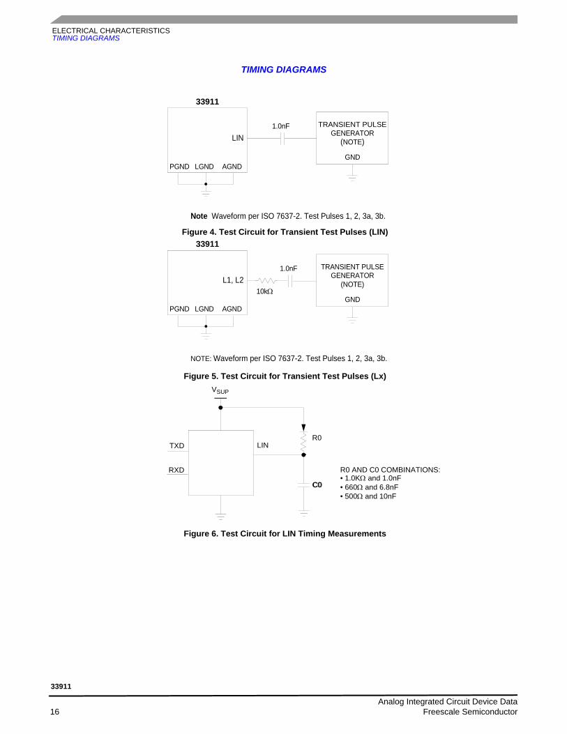
Figure 4. Test Circuit for Transient Test Pulses (LIN)
Figure 5. Test Circuit for Transient Test Pulses (Lx)
Figure 6. Test Circuit for LIN Timing Measurements
Note Waveform per ISO 7637-2. Test Pulses 1, 2, 3a, 3b.
LINTRANSIENT PULSE
PGND
GENERATOR1.0nF
(NOTE)
GND
33911
LGND AGND
L1, L2TRANSIENT PULSE
PGND
GENERATOR1.0nF
(NOTE)10kΩ
NOTE: Waveform per ISO 7637-2. Test Pulses 1, 2, 3a, 3b.
GND
33911
LGND AGND
R0 AND C0 COMBINATIONS:• 1.0KΩ and 1.0nF• 660Ω and 6.8nF• 500Ω and 10nF
VSUP
TXD
RXD
LINR0
C0C0
Analog Integrated Circuit Device Data 16 Freescale Semiconductor
33911
ELECTRICAL CHARACTERISTICSTIMING DIAGRAMS
Figure 7. LIN Timing Measurements for Normal Slew Rate
Figure 8. LIN Timing Measurements for Slow Slew Rate
TXD
LIN
RXD
tBIT tBIT
tBUS_DOM (MAX) tBUS_REC (MIN)
tREC - MAX
tDOM - MIN
tDOM - MIN
tRRECtRDOM
28.4% VSUP
58.1% VSUP40.0% VSUP
60.0% VSUP
74.4% VSUP
42.2% VSUP
40.0% VSUP
58.1% VSUP
28.4% VSUP
tBUS_DOM (MIN)tBUS_REC (MAX)
tDOM - MAX tREC - MIN
VLIN_REC
TXD
LIN
RXD
tBIT tBIT
tBUS_DOM (MAX) tBUS_REC (MIN)
tREC - MAX
tDOM - MIN
tDOM - MIN
tRRECtRDOM
25.1% VSUP
61.6% VSUP40.0% VSUP
60.0% VSUP
77.8% VSUP
38.9% VSUP
40.0% VSUP
61.6% VSUP
25.1% VSUP
tBUS_DOM (MIN)tBUS_REC (MAX)
tDOM - MAX tREC - MIN
VLIN_REC
Analog Integrated Circuit Device Data Freescale Semiconductor 17
33911
ELECTRICAL CHARACTERISTICSTIMING DIAGRAMS
Figure 9. LIN Receiver Timing
Figure 10. LIN Wake-Up Sleep Mode Timing
Figure 11. LIN Wake-Up Stop Mode Timing
VBUSrec
VBUSdom
VSUPLIN BUS SIGNAL
tRX_PDRtRX_PDF
RXD
VLIN_REC
DOMINANT LEVEL
0.4 VSUP
VLIN_REC
LIN
VDD
tPROPWL tWAKE
IRQ
LIN
Vrec
TpropWL Twake
Dominant level
0.4VSUP
Dominant Level
0.4 VSUP
tPROPWL tWAKE
VLIN_REC
Analog Integrated Circuit Device Data 18 Freescale Semiconductor
33911
ELECTRICAL CHARACTERISTICSTIMING DIAGRAMS
Figure 12. Power On Reset and Normal Request timeout Timing
Figure 13. SPI Timing Characteristics
VSUP
VDD
RST
tRSTtNRTOUT
D0
D0
UNDEFINED DON’T CARE D7 DON’T CARE
tLEAD
tSIHtSISU
tLAG
tPSCLK
tWSCLKH
tWSCLKL
tVALID
DON’T CARE D7
tSODIS
CS
SCLK
MOSI
MISO
tSOEN
Analog Integrated Circuit Device Data Freescale Semiconductor 19
33911
FUNCTIONAL DESCRIPTIONINTRODUCTION
FUNCTIONAL DESCRIPTION
INTRODUCTION
The 33911 was designed and developed as a highly integrated and cost-effective solution for automotive and industrial applications. For automotive body electronics, the 33911 is well suited to perform relay control in applications like window lift, sunroof, etc. via a LIN bus.
Power switches are provided on the device configured as high side and low side outputs. Other ports are also provided,
which include a voltage sense port and two wake-up capable pins. An internal voltage regulator provides power to a MCU device.
Also included in this device is a LIN physical layer, which communicates using a single wire. This enables this device to be compatible with 3-wire bus systems, where one wire is used for communication, one for battery, and one for ground.
FUNCTIONAL PIN DESCRIPTION
See Figure 1, 33911 Simplified Application Diagram, page 1, for a graphic representation of the various pins referred to in the following paragraphs. Also, see the pin diagram on page 3 for a description of the pin locations in the package.
RECEIVER OUTPUT (RXD)The RXD pin is a digital output. It is the receiver output of
the LIN interface and reports the state of the bus voltage: RXD Low when LIN bus is dominant, RXD High when LIN bus is recessive.
TRANSMITTER INPUT (TXD)The TXD pin is a digital input. It is the transmitter input of
the LIN interface and controls the state of the bus output (dominant when TXD is Low, recessive when TXD is High).
This pin has an internal pull-up to force recessive state in case the input is left floating.
LIN BUS (LIN)The LIN pin represents the single-wire bus transmitter and
receiver. It is suited for automotive bus systems and is compliant to the LIN bus specification 2.0.
The LIN interface is only active during Normal and Normal Request Modes.
SERIAL DATA CLOCK (SCLK)The SCLK pin is the SPI clock input pin. MISO data
changes on the negative transition of the SCLK. MOSI is sampled on the positive edge of the SCLK.
MASTER OUT SLAVE IN (MOSI)The MOSI digital pin receives SPI data from the MCU. This
data input is sampled on the positive edge of SCLK.
MASTER IN SLAVE OUT (MISO)The MISO pin sends data to a SPI-enabled MCU. It is a
digital tri-state output used to shift serial data to the
microcontroller. Data on this output pin changes on the negative edge of the SCLK. When CS is High, this pin will remain in high-impedance state.
CHIP SELECT (CS)CS is an active low digital input. It must remain low during
a valid SPI communication and allow for several devices to be connected in the same SPI bus without contention. A rising edge on CS signals the end of the transmission and the moment the data shifted in is latched. A valid transmission must consist of 8 bits only.
While in STOP Mode a low-to-high level transition on this pin will generate a wake-up condition.
ANALOG MULTIPLEXER (ADOUT0)The ADOUT0 pin can be configured via the SPI to allow
the MCU A/D converter to read the several inputs of the Analog Multiplexer, including the VSENSE, L1, L2 input voltages and the internal junction temperature.
PWM INPUT CONTROL (PWMIN)This digital input can control the high side and low side
drivers in Normal Request and Normal Mode.To enable PWM control, the MCU must perform a write
operation to the High Side Control Register (HSCR), or the Low Side Control Register (LSCR).
This pin has an internal 20µA current pull-up.
RESET (RST)This bidirectional pin is used to reset the MCU in case the
33911 detects a reset condition, or to inform the 33911 that the MCU was just reset. After release of the RST pin Normal Request Mode is entered.
The RST pin is an active low filtered input and output formed by a weak pull-up and a switchable pull-down structure, which allows this pin to be shorted either to VDD or to GND during software development without the risk of destroying the driver.
Analog Integrated Circuit Device Data 20 Freescale Semiconductor
33911
FUNCTIONAL DESCRIPTIONFUNCTIONAL PIN DESCRIPTION
INTERRUPT (IRQ)The IRQ pin is a digital output used to signal events or
faults to the MCU while in Normal and Normal Request Mode or to signal a wake-up from Stop Mode. This active low output will transition high only after the interrupt is acknowledged by a SPI read of the respective status bits.
WATCHDOG CONFIGURATION (WDCONF)The WDCONF pin is the configuration pin for the internal
watchdog. A resistor can be connected to this pin to configure the window watchdog period. When connected directly to ground, the watchdog will be disabled. When this pin is left open, the watchdog period is fixed to its lower precision internal default value (150ms, typical).
GROUND CONNECTIONS (AGND, PGND, LGND)The AGND, PGND and LGND pins are the Analog and
Power ground pins. The AGND pin is the ground reference of the voltage
regulator. The PGND and LGND pins are used for high-current load
return as in the relay-drivers and LIN interface pin.Note: PGND, AGND and LGND pins must be connected
together.
LOW SIDES (LS1 AND LS2)LS1 and LS2 are the low side driver outputs. Those
outputs are short-circuit protected and include active clamp circuitry to drive inductive loads. Due to the energy clamp voltage on this pin, it can raise above the battery level when switched off. The switches are controlled through the SPI and can be configured to respond to a signal applied to the PWMIN input pin.
Both low side switches are protected against overheating.
DIGITAL/ANALOGS (L1 AND L2)The Lx pins are multi purpose inputs. They can be used as
digital inputs, which can be sampled by reading the SPI and used for wake-up when 33911 is in low-power mode or used as analog inputs for the analog multiplexer. When used to sense voltage outside the module, a 33kohm series resistor must be used on each input.
When used as wake-up inputs L1 and L2 can be configured to operate in cyclic sense mode. In this mode, the high side switch is configured to be periodically turned on and sample the wake-up inputs. If a state change is detected between two cycles, a wake-up is initiated. The 33911 can also wake-up from Stop or Sleep by a simple state change on L1 and L2.
When used as an analog input, the voltage present on the Lx pins are scaled down by a selectable internal voltage
divider and can be routed to the ADOUT0 output through the analog multiplexer.
Note: If an Lx input is selected in the analog multiplexer, it will be disabled as a digital input and remains disabled in low-power mode. No wake-up feature is available in that condition.
When an Lx input is not selected in the analog multiplexer, the voltage divider is disconnected from that input.
HIGH SIDE OUTPUT (HS1)This high side switch is able to drive loads such as relays
or lamps. Its structure is connected to the VS2 supply pin. The pin is short-circuit protected and also protected against overheating.
HS1 is controlled by SPI and can respond to a signal applied to the PWMIN input pin.
The HS1 output can also be used during low-power mode for the cyclic-sense of the wake inputs.
POWER SUPPLIES (VS1 AND VS2)These are the battery level voltage supply pins. In
application, VS1 and VS2 pins must be protected against a reverse battery connection and negative transient voltages with external components. These pins sustain standard automotive voltage conditions such as a load dump at 40V.
The high side switch (HS1) is supplied by the VS2 pin, all other internal blocks are supplied by the VS1 pin.
VOLTAGE SENSE (VSENSE)This input can be connected directly to the battery line. It
is protected against a battery reverse connection. The voltage present on this input is scaled down by an internal voltage divider, and can be routed to the ADOUT0 output pin and used by the MCU to read the battery voltage.
The ESD structure on this pin allows for excursion up to +40V and down to -27V, allowing this pin to be connected directly to the battery line. It is strongly recommended to connect a 10kohm resistor in series with this pin for protection purposes.
+5V MAIN REGULATOR OUTPUT (VDD)An external capacitor must be placed on the VDD pin to
stabilize the regulated output voltage. The VDD pin is intended to supply a microcontroller. The pin is current limited against shorts to GND and over-temperature protected.
During Stop Mode, the voltage regulator does not operate with its full drive capabilities and the output current is limited.
During Sleep Mode the regulator output is completely shut down.
Analog Integrated Circuit Device Data Freescale Semiconductor 21
33911
FUNCTIONAL DESCRIPTIONFUNCTIONAL INTERNAL BLOCK DESCRIPTION
FUNCTIONAL INTERNAL BLOCK DESCRIPTION
Figure 14. Functional Internal Block Diagram
ANALOG CIRCUITRYThe 33911 is designed to operate under automotive
operating conditions. A fully configurable window watchdog circuit will reset the connected MCU in case of an overflow.
Two low-power modes are available with several different wake-up sources to reactivate the device. Two analog / digital inputs can be sensed or used as the wake-up source.
The device is capable of sensing the supply voltage (VSENSE), the internal chip temperature (CTEMP) as well as the motor current using an external sense resistor.)
HIGH SIDE DRIVEROne current and temperature protected high side driver
with PWM capability is provided to drive small loads such as status LED’s or small lamps.
The driver can be configured for periodic sense during low-power modes.
LOW SIDE DRIVERSTwo current and temperature protected low side
drivers with PWM capability are provided to drive H-Bridge type relays for power motor applications.
MCU INTERFACEThe 33911 is providing its control and status information
through a standard 8-Bit SPI interface. Critical system events such as low or high-voltage/temperature conditions as well as over-current conditions in any of the driver stages can be reported to the connected MCU via IRQ or RST.
Both low side and both high side driver outputs can be controlled via the SPI register as well as PWMIN input.
The integrated LIN physical layer interface can be configured via the SPI register and its communication is driven through the RXD and TXD device pin.
All internal analog sources are multiplexed to the ANOUT0 pin.
VOLTAGE REGULATOR OUTPUTSOne voltage regulators is implemented on the 33911. The
VDD main regulator output is designed to supply an MCU with a precise 5V.
LIN PHYSICAL LAYER INTERFACEThe 33911 provides a LIN 2.0 compatible LIN physical
layer interface with selectable slew rate and various diagnostic features.
MC33911 - Functional Block Diagram
Integrated Supply
Voltage Regulator VDD
High Side Driver
HS1
LIN Physical Layer
Interface
Low Side Drivers
LS1 - LS2
Analog Circuitry
Digital / Analog Input
Voltage & Temperature Sense
Wake-UpWindow Watchdog
Analog CircuitryMCU Interface and Output ControlDrivers
MCU Interface and Output Control
SPI Interface
Integrated Supply
Reset & IRQ Logic
LIN Interface / Control
Analog Output 0
LS/HS - PWM Control
Analog Integrated Circuit Device Data 22 Freescale Semiconductor
33911
FUNCTIONAL DEVICE OPERATIONSOPERATIONAL MODES
FUNCTIONAL DEVICE OPERATIONS
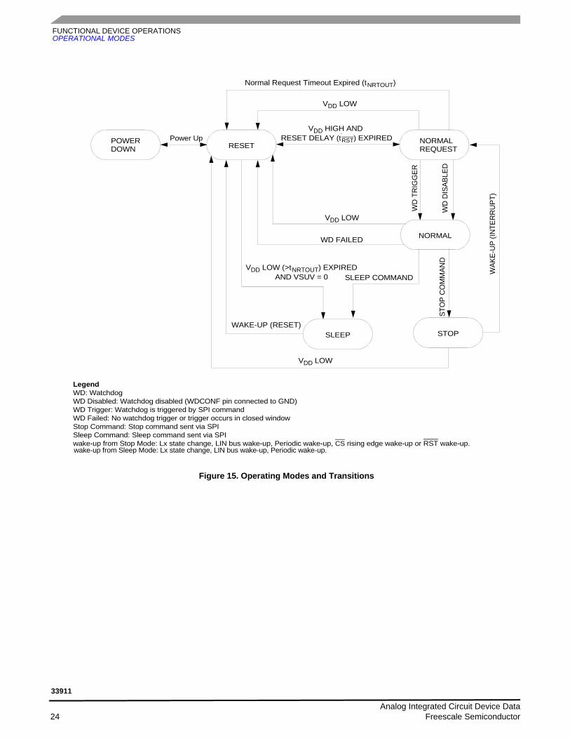
OPERATIONAL MODES
INTRODUCTIONThe 33911 offers three main operating modes: Normal
(Run), Stop, and Sleep (Low-power). In Normal Mode, the device is active and operating under normal application conditions. The Stop and Sleep Modes are low-power modes with wake-up capabilities.
In Stop Mode, the voltage regulator still supplies the MCU with VDD (limited current capability), and in Sleep Mode the voltage regulator is turned off (VDD = 0V).
Wake-up from Stop Mode is initiated by a wake-up interrupt. Wake-up from Sleep Mode is done by a reset and the voltage regulator is turned back on.
The selection of the different modes is controlled by the MOD1:2 bits in the Mode Control Register (MCR).
Figure 15 describes how transitions are done between the different operating modes, and Table 5, 25, gives an overview of the operating modes.
RESET MODEThe 33911 enters the Reset Mode after a power up. In this
mode, the RST pin is low for 1ms (typical value). After this delay, the 33911 enters the Normal Request Mode and the RST pin is driven high.
The Reset Mode is entered if a reset condition occurs (VDD low, Watchdog trigger fail, after a wake-up from Sleep Mode, or a Normal Request Mode timeout).
NORMAL REQUEST MODEThis is a temporary mode automatically accessed by the
device after the Reset Mode, or after a wake-up from Stop Mode.
In Normal Request Mode, the VDD regulator is ON, the Reset pin is high and the LIN is operating in RX Only Mode.
As soon as the device enters the Normal Request Mode, an internal timer is started for 150ms (typical value). During these 150ms, the MCU must configure the Timing Control Register (TIMCR) and the MCR with MOD2 and MOD1 bits set = 0, to enter in Normal Mode. If within the 150ms timeout the MCU does not command the 33911 to Normal Mode, it will enter in Reset Mode. If the WDCONF pin is grounded in order to disable the watchdog function, the 33911 goes directly in Normal Mode after the Reset Mode. If the WDCONF pin is open, the 33911 stays typically for 150ms in Normal Request before entering in Normal Mode.
NORMAL MODEIn Normal Mode, all 33911 functions are active and can be
controlled by the SPI interface and the PWMIN pin.
The VDD regulator is ON and delivers its full current capability.
If an external resistor is connected between the WDCONF pin and the Ground, the window watchdog function will be enabled.
The wake-up inputs (L1 and L2) can be read as digital inputs or have its voltage routed through the analog multiplexer.
The LIN interface has slew rate and timing compatible with the LIN protocol specification 2.0. The LIN bus can transmit and receive information.
The high side and the low side switches are active and have PWM capability according to the SPI configuration.
The interrupts are generated to report failures for VSUP over/under-voltage, thermal shutdown or thermal shutdown prewarning on the main regulator.
SLEEP MODEThe Sleep Mode is a low-power mode. From Normal
Mode, the device enters the Sleep Mode by sending one SPI command through the MCR. All blocks are in their lowest power consumption condition. Only some wake-up sources (wake-up inputs with or without cyclic sense, forced wake-up, and LIN receiver) are active. The 5V regulator is OFF. The internal low-power oscillator may be active if the IC is configured for cyclic sense. In this condition, the high side switches are turned on periodically and the wake-up inputs are sampled.
Wake-up from Sleep Mode is similar to a power-up. The device goes into Reset Mode except that the SPI will report the wake-up source, and the BATFAIL flag is not set.
STOP MODEThe Stop Mode is the second low-power mode, but in this
case the 5V regulator is ON with limited current drive capability. The application MCU is always supplied while the 33911 is operating in Stop Mode.
The device can enter the Stop Mode only by sending a SPI command. When the application is in this mode, it can wake-up from the 33911 side (for example: cyclic sense, force wake-up, LIN bus, wake inputs) or the MCU side (CS, RST pins). Wake-up from Stop Mode will transition the 33911 to Normal Request Mode and generate an interrupt, except if the wake-up event is a low to high transition on the CS pin or comes from the RST pin.
Analog Integrated Circuit Device Data Freescale Semiconductor 23
33911
FUNCTIONAL DEVICE OPERATIONSOPERATIONAL MODES
Figure 15. Operating Modes and Transitions
Normal Request Timeout Expired (tNRTOUT)
VDD HIGH AND RESET DELAY (tRST) EXPIRED
VDD LOW
VDD LOW
WD FAILED
VDD LOW (>tNRTOUT) EXPIREDAND VSUV = 0 SLEEP COMMAND
STO
P C
OM
MAN
D
WAKE-UP (RESET)
WD
TR
IGG
ER
WD
DIS
ABLE
D
Power Up
WAK
E-U
P (IN
TER
RU
PT)
LegendWD: WatchdogWD Disabled: Watchdog disabled (WDCONF pin connected to GND)WD Trigger: Watchdog is triggered by SPI commandWD Failed: No watchdog trigger or trigger occurs in closed windowStop Command: Stop command sent via SPISleep Command: Sleep command sent via SPIwake-up from Stop Mode: Lx state change, LIN bus wake-up, Periodic wake-up, CS rising edge wake-up or RST wake-up.
VDD LOW
wake-up from Sleep Mode: Lx state change, LIN bus wake-up, Periodic wake-up.
POWERDOWN
NORMALREQUESTRESET
NORMAL
SLEEP STOP
Analog Integrated Circuit Device Data 24 Freescale Semiconductor
33911
FUNCTIONAL DEVICE OPERATIONSOPERATIONAL MODES
INTERRUPTSInterrupts are used to signal a microcontroller that a
peripheral needs to be serviced. The interrupts which can be generated change according to the operating mode. While in Normal and Normal Request Modes, the 33911 signals through interrupts special conditions which may require a MCU software action. Interrupts are not generated until all pending wake-up sources are read in the Interrupt Source Register (ISR).
While in Stop Mode, interrupts are used to signal wake-up events. Sleep Mode does not use interrupts, wake-up is performed by powering-up the MCU. In Normal and Normal Request mode the wake-up source can be read by the SPI.
The interrupts are signaled to the MCU by a low logic level of the IRQ pin, which will remain low until the interrupt is acknowledged by a SPI read. The IRQ pin will then be driven high.
Interrupts are only asserted while in Normal, Normal Request and Stop mode. Interrupts are not generated while the RST pin is low.
Following is a list of the interrupt sources in Normal and Normal Request Modes, some of those can be masked by writing to the SPI-Interrupt Mask Register (IMR).
Low-voltage InterruptThe low-voltage interrupt signals when the supply line
(VS1) voltage drops below the VSUV threshold (VSUV).
High-voltage InterruptThe high-voltage interrupt signals when the supply line
(VS1) voltage increases above the VSOV threshold (VSOV).
Over-temperature PrewarningOver-temperature prewarning signals when the 33911
temperature has reached the pre-shutdown warning threshold. It is used to warn the MCU that an over-temperature shutdown in the main 5V regulator is imminent.
LIN Over-current Shutdown / Over-temperature Shutdown / TXD Stuck At Dominant / RXD Short-Circuit
These signal fault conditions within the LIN interface will cause the LIN driver to be disabled, except for the LIN over-current. In order to restart an operation, the fault must be removed and must be acknowledged by reading the SPI.
The LINOC bit functionality in the LIN Status Register (LINSR) is to indicate that an LIN over-current occurred and the driver stays enabled.
High Side Over-temperature ShutdownThe high side over-temperature shutdown signals a
shutdown in the high side output.
Low Side Over-temperature ShutdownThe low side over-temperature shutdown signals a
shutdown in the low side outputs.
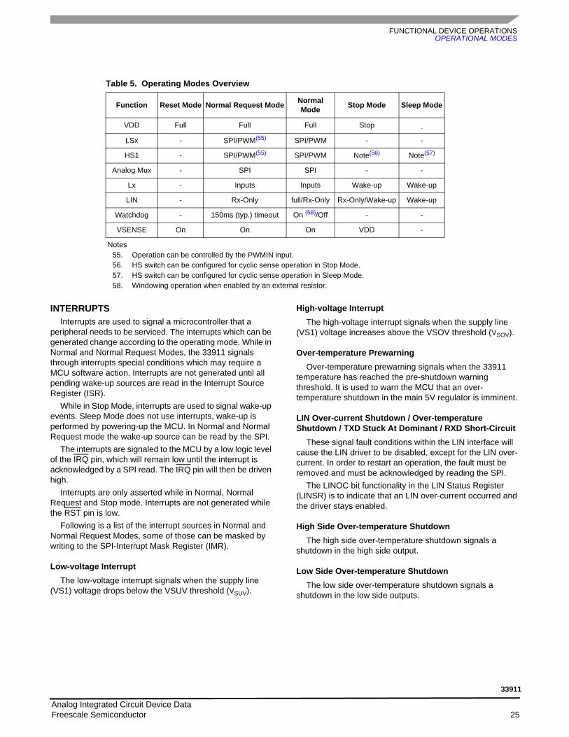
Table 5. Operating Modes Overview
Function Reset Mode Normal Request Mode Normal Mode Stop Mode Sleep Mode
VDD Full Full Full Stop -
LSx - SPI/PWM(55) SPI/PWM - -
HS1 - SPI/PWM(55) SPI/PWM Note(56) Note(57)
Analog Mux - SPI SPI - -
Lx - Inputs Inputs Wake-up Wake-up
LIN - Rx-Only full/Rx-Only Rx-Only/Wake-up Wake-up
Watchdog - 150ms (typ.) timeout On (58)/Off - -
VSENSE On On On VDD -
Notes55. Operation can be controlled by the PWMIN input.56. HS switch can be configured for cyclic sense operation in Stop Mode.57. HS switch can be configured for cyclic sense operation in Sleep Mode.58. Windowing operation when enabled by an external resistor.
Analog Integrated Circuit Device Data Freescale Semiconductor 25
33911
FUNCTIONAL DEVICE OPERATIONSOPERATIONAL MODES
RESETTo reset an MCU, the 33911 drives the RST pin low for the
time the reset condition lasts. After the reset source has been removed, the state
machine will drive the RST output low for at least 1ms (typical value) before driving it high.
In the 33911 four main reset sources exist:
5V Regulator Low-voltage-Reset (VRSTTH)The 5V regulator output VDD is continuously monitored
against brown outs. If the supply monitor detects that the voltage at the VDD pin has dropped below the reset threshold VRSTTH the 33911 will issue a reset. In case of an over-temperature, the voltage regulator will be disabled and the voltage monitoring will issue a VDDOT Flag independently of the VDD voltage.
Window Watchdog OverflowIf the watchdog counter is not properly serviced while its
window is open, the 33911 will detect an MCU software run-away and will reset the microcontroller.
Wake-Up From Sleep ModeDuring Sleep Mode, the 5V regulator is not active. Hence,
all wake-up requests from Sleep Mode require a power-up/reset sequence.
External ResetThe 33911 has a bidirectional reset pin which drives the
device to a safe state (same as Reset Mode) for as long as this pin is held low. The RST pin must be held low long enough to pass the internal glitch filter and get recognized by the internal reset circuit. This functionality is also active in Stop Mode.
After the RST pin is released, there is no extra t RST to be considered.
WAKE-UP CAPABILITIESOnce entered into one of the low-power modes (Sleep or
Stop) only wake-up sources can bring the device into Normal Mode operation.
In Stop Mode, a wake-up is signaled to the MCU as an interrupt, while in Sleep Mode, the wake-up is performed by activating the 5V regulator and resetting the MCU. In both cases, the MCU can detect the wake-up source by accessing the SPI registers. There is no specific SPI register bit to signal a CS wake-up or external reset. If necessary, this condition is detected by excluding all other possible wake-up sources.
Wake-up from Wake-up inputs (L1-L2) with cyclic sense disabled
The wake-up lines are dedicated to sense state changes of external switches, and wake-up the MCU (in Sleep or Stop Mode).
In order to select and activate direct wake-up from Lx inputs, the Wake-up Control Register (WUCR) must be configured with appropriate LxWE inputs enabled or disabled. The wake-up inputs state are read through the Wake-up Status Register (WUSR).
Lx inputs are also used to perform cyclic sense wake-up.Note: Selecting an Lx input in the analog multiplexer
before entering low-power mode will disable the wake-up capability of the Lx input.
Wake-up from Wake-up inputs (L1-L2) with cyclic sense timer enabled
The SBCLIN can wake-up at the end of a cyclic sense period if on one of the two wake-up input lines (L1-L2), a state change occurs. The HS1 switch is activated in Sleep or Stop Modes from an internal timer. Cyclic sense and force wake-up are exclusive. If cyclic sense is enabled, the force wake-up can not be enabled.
In order to select and activate the cyclic sense wake-up from Lx inputs, before entering in low-power modes (Stop or Sleep Modes), the following SPI set-up has to be performed:
• In WUCR: select the Lx input to WU-enable.• In HSCR: enable HS1.• In TIMCR: select the CS/WD bit and determine the
cyclic sense period with CYSTx bits.• Perform Goto Sleep/Stop command.
Forced Wake-upThe 33911 can wake-up automatically after a
predetermined time spent in Sleep or Stop Mode. Cyclic sense and forced wake-up are exclusive. If forced wake-up is enabled, the cyclic sense can not be enabled.
To determine the wake-up period, the following SPI set-up has to be sent before entering in low-power modes:
• In TIMCR: select the CS/WD bit and determine the low-power mode period with CYSTx bits.
• In HSCR: the HS1 bit must be disabled.
CS Wake-upWhile in Stop Mode, a rising edge on the CS will cause a
wake-up. The CS wake-up does not generate an interrupt and is not reported on the SPI.
LIN Wake-upWhile in the low-power mode the 33911 monitors the
activity on the LIN bus. A dominant pulse larger than t PROPWL followed by a dominant to recessive transition will cause a LIN wake-up. This behavior protects the system from a short-to ground bus condition.
Analog Integrated Circuit Device Data 26 Freescale Semiconductor
33911
FUNCTIONAL DEVICE OPERATIONSOPERATIONAL MODES
RST Wake-upWhile in Stop Mode, the 33911 can wake-up when the
RST pin is held low long enough to pass the internal glitch filter. Then, it will change to Normal Request or Normal Modes depending on the WDCONF pin configuration. The RST wake-up does not generate an interrupt and is not reported via the SPI.
From Stop Mode, the following wake-up events can be configured:
• Wake-up from Lx inputs without cyclic sense• Cyclic sense wake-up inputs• Force wake-up• CS wake-up• LIN wake-up• RST wake-upFrom Sleep Mode, the following wake-up events can be
configured:• Wake-up from Lx inputs without cyclic sense• Cyclic sense wake-up inputs• Force wake-up• LIN wake-up
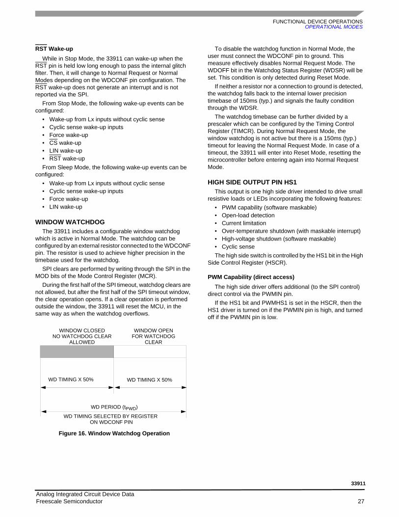
WINDOW WATCHDOGThe 33911 includes a configurable window watchdog
which is active in Normal Mode. The watchdog can be configured by an external resistor connected to the WDCONF pin. The resistor is used to achieve higher precision in the timebase used for the watchdog.
SPI clears are performed by writing through the SPI in the MOD bits of the Mode Control Register (MCR).
During the first half of the SPI timeout, watchdog clears are not allowed, but after the first half of the SPI timeout window, the clear operation opens. If a clear operation is performed outside the window, the 33911 will reset the MCU, in the same way as when the watchdog overflows.
Figure 16. Window Watchdog Operation
To disable the watchdog function in Normal Mode, the user must connect the WDCONF pin to ground. This measure effectively disables Normal Request Mode. The WDOFF bit in the Watchdog Status Register (WDSR) will be set. This condition is only detected during Reset Mode.
If neither a resistor nor a connection to ground is detected, the watchdog falls back to the internal lower precision timebase of 150ms (typ.) and signals the faulty condition through the WDSR.
The watchdog timebase can be further divided by a prescaler which can be configured by the Timing Control Register (TIMCR). During Normal Request Mode, the window watchdog is not active but there is a 150ms (typ.) timeout for leaving the Normal Request Mode. In case of a timeout, the 33911 will enter into Reset Mode, resetting the microcontroller before entering again into Normal Request Mode.
HIGH SIDE OUTPUT PIN HS1This output is one high side driver intended to drive small
resistive loads or LEDs incorporating the following features:• PWM capability (software maskable) • Open-load detection• Current limitation• Over-temperature shutdown (with maskable interrupt)• High-voltage shutdown (software maskable)• Cyclic senseThe high side switch is controlled by the HS1 bit in the High
Side Control Register (HSCR).
PWM Capability (direct access)The high side driver offers additional (to the SPI control)
direct control via the PWMIN pin. If the HS1 bit and PWMHS1 is set in the HSCR, then the
HS1 driver is turned on if the PWMIN pin is high, and turned off if the PWMIN pin is low.
WD PERIOD (tPWD)
WINDOW CLOSEDNO WATCHDOG CLEAR
ALLOWED
WINDOW OPENFOR WATCHDOG
CLEAR
WD TIMING X 50% WD TIMING X 50%
WD TIMING SELECTED BY REGISTER ON WDCONF PIN
Analog Integrated Circuit Device Data Freescale Semiconductor 27
33911
FUNCTIONAL DEVICE OPERATIONSOPERATIONAL MODES
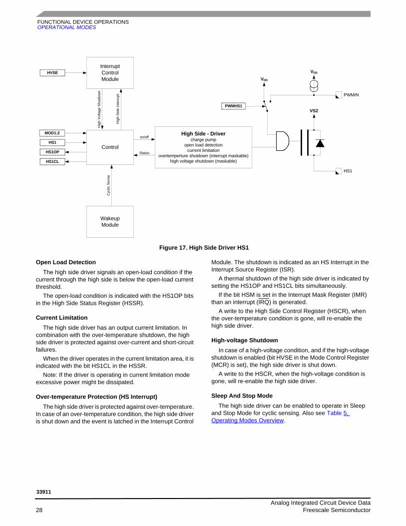
Figure 17. High Side Driver HS1
Open Load DetectionThe high side driver signals an open-load condition if the
current through the high side is below the open-load current threshold.
The open-load condition is indicated with the HS1OP bits in the High Side Status Register (HSSR).
Current Limitation The high side driver has an output current limitation. In
combination with the over-temperature shutdown, the high side driver is protected against over-current and short-circuit failures.
When the driver operates in the current limitation area, it is indicated with the bit HS1CL in the HSSR.
Note: If the driver is operating in current limitation mode excessive power might be dissipated.
Over-temperature Protection (HS Interrupt)The high side driver is protected against over-temperature.
In case of an over-temperature condition, the high side driver is shut down and the event is latched in the Interrupt Control
Module. The shutdown is indicated as an HS Interrupt in the Interrupt Source Register (ISR).
A thermal shutdown of the high side driver is indicated by setting the HS1OP and HS1CL bits simultaneously.
If the bit HSM is set in the Interrupt Mask Register (IMR) than an interrupt (IRQ) is generated.
A write to the High Side Control Register (HSCR), when the over-temperature condition is gone, will re-enable the high side driver.
High-voltage ShutdownIn case of a high-voltage condition, and if the high-voltage
shutdown is enabled (bit HVSE in the Mode Control Register (MCR) is set), the high side driver is shut down.
A write to the HSCR, when the high-voltage condition is gone, will re-enable the high side driver.
Sleep And Stop ModeThe high side driver can be enabled to operate in Sleep
and Stop Mode for cyclic sensing. Also see Table 5, Operating Modes Overview.
High Side - Drivercharge pump
open load detectioncurrent limitation
overtemperture shutdown (interrupt maskable)high voltage shutdown (maskable)
Control
on/off
Status
PWMIN
VDD
PWMHS1
HS1
HVSE
HS1OP
HS1CL
MOD1:2
InterruptControl Module
HS1
VS2
Hig
h V
olta
ge S
hutd
own
Hig
h-S
ide
Inte
rrupt
VDD
WakeupModule
Cyc
lic S
ense
Analog Integrated Circuit Device Data 28 Freescale Semiconductor
33911
FUNCTIONAL DEVICE OPERATIONSOPERATIONAL MODES
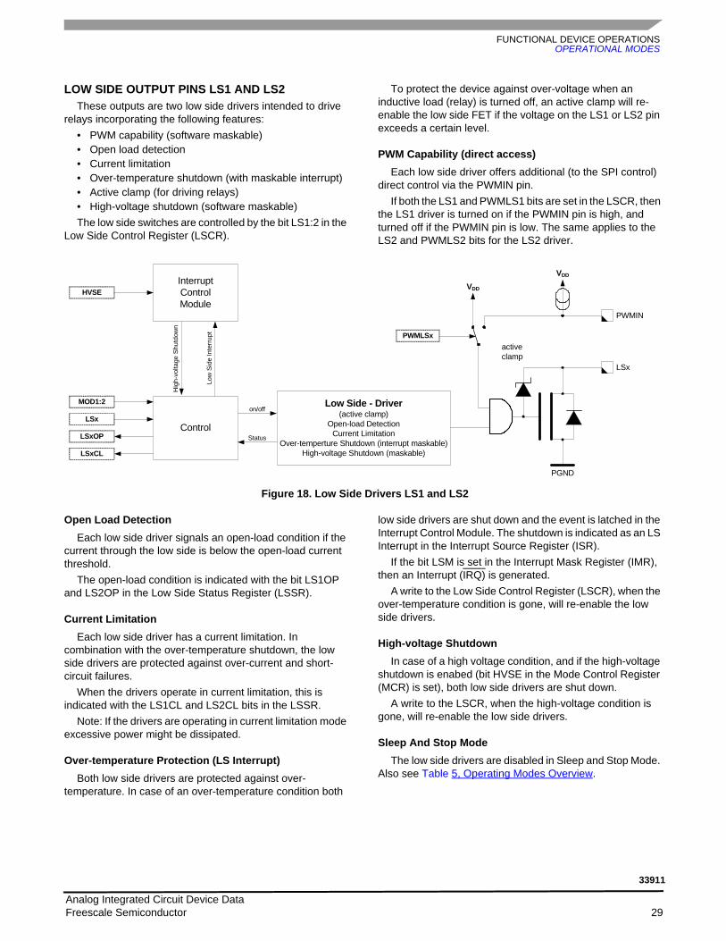
LOW SIDE OUTPUT PINS LS1 AND LS2These outputs are two low side drivers intended to drive
relays incorporating the following features:• PWM capability (software maskable)• Open load detection• Current limitation• Over-temperature shutdown (with maskable interrupt)• Active clamp (for driving relays)• High-voltage shutdown (software maskable)The low side switches are controlled by the bit LS1:2 in the
Low Side Control Register (LSCR).
To protect the device against over-voltage when an inductive load (relay) is turned off, an active clamp will re-enable the low side FET if the voltage on the LS1 or LS2 pin exceeds a certain level.
PWM Capability (direct access)Each low side driver offers additional (to the SPI control)
direct control via the PWMIN pin. If both the LS1 and PWMLS1 bits are set in the LSCR, then
the LS1 driver is turned on if the PWMIN pin is high, and turned off if the PWMIN pin is low. The same applies to the LS2 and PWMLS2 bits for the LS2 driver.
Figure 18. Low Side Drivers LS1 and LS2
Open Load DetectionEach low side driver signals an open-load condition if the
current through the low side is below the open-load current threshold.
The open-load condition is indicated with the bit LS1OP and LS2OP in the Low Side Status Register (LSSR).
Current Limitation Each low side driver has a current limitation. In
combination with the over-temperature shutdown, the low side drivers are protected against over-current and short-circuit failures.
When the drivers operate in current limitation, this is indicated with the LS1CL and LS2CL bits in the LSSR.
Note: If the drivers are operating in current limitation mode excessive power might be dissipated.
Over-temperature Protection (LS Interrupt)Both low side drivers are protected against over-
temperature. In case of an over-temperature condition both
low side drivers are shut down and the event is latched in the Interrupt Control Module. The shutdown is indicated as an LS Interrupt in the Interrupt Source Register (ISR).
If the bit LSM is set in the Interrupt Mask Register (IMR), then an Interrupt (IRQ) is generated.
A write to the Low Side Control Register (LSCR), when the over-temperature condition is gone, will re-enable the low side drivers.
High-voltage ShutdownIn case of a high voltage condition, and if the high-voltage
shutdown is enabed (bit HVSE in the Mode Control Register (MCR) is set), both low side drivers are shut down.
A write to the LSCR, when the high-voltage condition is gone, will re-enable the low side drivers.
Sleep And Stop ModeThe low side drivers are disabled in Sleep and Stop Mode.
Also see Table 5, Operating Modes Overview.
LSx
Low Side - Driver(active clamp)
Open-load DetectionCurrent Limitation
Over-temperture Shutdown (interrupt maskable)High-voltage Shutdown (maskable)
PGND
active clamp
InterruptControl Module
HVSE
Control
on/off
Status
LSx
LSxOP
LSxCL
MOD1:2
Hig
h-vo
ltage
Shu
tdow
n
Low
Sid
e In
terr
upt
PWMIN
VDD
PWMLSx
VDD
Analog Integrated Circuit Device Data Freescale Semiconductor 29
33911
FUNCTIONAL DEVICE OPERATIONSOPERATIONAL MODES
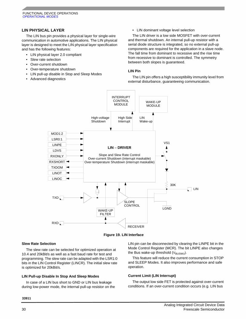
LIN PHYSICAL LAYERThe LIN bus pin provides a physical layer for single-wire
communication in automotive applications. The LIN physical layer is designed to meet the LIN physical layer specification and has the following features:
• LIN physical layer 2.0 compliant• Slew rate selection• Over-current shutdown• Over-temperature shutdown• LIN pull-up disable in Stop and Sleep Modes• Advanced diagnostics
• LIN dominant voltage level selectionThe LIN driver is a low side MOSFET with over-current
and thermal shutdown. An internal pull-up resistor with a serial diode structure is integrated, so no external pull-up components are required for the application in a slave node. The fall time from dominant to recessive and the rise time from recessive to dominant is controlled. The symmetry between both slopes is guaranteed.
LIN PinThe LIN pin offers a high susceptibility immunity level from
external disturbance, guaranteeing communication.
Figure 19. LIN Interface
Slew Rate SelectionThe slew rate can be selected for optimized operation at
10.4 and 20kBit/s as well as a fast baud rate for test and programming. The slew rate can be adapted with the LSR1:0 bits in the LIN Control Register (LINCR). The initial slew rate is optimized for 20kBit/s.
LIN Pull-up Disable In Stop And Sleep ModesIn case of a LIN bus short to GND or LIN bus leakage
during low-power mode, the internal pull-up resistor on the
LIN pin can be disconnected by clearing the LINPE bit in the Mode Control Register (MCR). The bit LINPE also changes the Bus wake-up threshold (VBUSWU).
This feature will reduce the current consumption in STOP and SLEEP Modes. It also improves performance and safe operation.
Current Limit (LIN Interrupt)The output low side FET is protected against over-current
conditions. If an over-current condition occurs (e.g. LIN bus
High-voltage High Side
RXONLY
MOD1:2
LSR0:1
LINPE
LDVS
INTERRUPTCONTROLMODULE
LIN – DRIVER
Slope and Slew Rate ControlOver-current Shutdown (interrupt maskable)
Over-temperature Shutdown (interrupt maskable)
VS1
WAKE-UP
RXSHORT
LINOC
TXDOM
LINOT
LIN
FILTER
SLOPECONTROL
30K
LGND
LIN
RECEIVER
TXD
RXD
InterruptShutdown Wake-up
WAKE-UPMODULE
Analog Integrated Circuit Device Data 30 Freescale Semiconductor
33911
FUNCTIONAL DEVICE OPERATIONSOPERATIONAL MODES
short to VBAT), the transmitter will not be shut down. The bit LINOC in the LIN Status Register (LINSR) is set.
If the LINM bit is set in the Interrupt Mask Register (IMR) an Interrupt IRQ will be generated.
Over-temperature Shutdown (LIN Interrupt)The output low side FET is protected against over-
temperature conditions. If an over-temperature condition occurs, the transmitter will be shut down and the LINOT bit in the LINSR is set.
If the LINM bit is set in the IMR an Interrupt IRQ will be generated.
The transmitter is automatically re-enabled once the condition is gone and TXD is high.
A read of the LINSR with the TXD pin high will re-enable the transmitter.
RXD Short-circuit Detection (LIN Interrupt)The LIN transceiver has a short-circuit detection for the
RXD output pin. In case of a short-circuit condition, either 5V or Ground, the RXSHORT bit in the LINSR is set and the transmitter is shutdown.
If the LINM bit is set in the IMR an Interrupt IRQ will be generated.
The transmitter is automatically re-enabled once the condition is gone (transition on RXD) and TXD is high.
A read of the LINSR without the RXD pin short-circuit condition will clear the RXSHORT bit.
TXD Dominant Detection (LIN Interrupt)The LIN transceiver monitors the TXD input pin to detect
stuck-in-dominant (0V) condition. If a stuck condition occurs (TXD pin 0V for more than 1 second (typ.), the transmitter is shut down and the TXDOM bit in the LINSR is set.
If the bit LINM is set in the IMR an Interrupt IRQ will be generated.
The transmitter is automatically re-enabled once TXD is high.
A read of the LINSR with the TXD pin is high will clear the bit TXDOM.
LIN Dominant Voltage Level SelectionThe LIN dominant voltage level can be selected by the
LDVS bit in the LIN Control Register (LINCR).
LIN Receiver Operation OnlyWhile in Normal Mode, the activation of the RXONLY bit
disables the LIN TXD driver. If a LIN error condition occurs, this bit is automatically set. Ifa low-power mode is selected with this bit set, the LIN wake-up functionality is disabled. Then in STOP mode, the RXD pin will reflect the state of the LIN bus.
STOP Mode And Wake-up FeatureDuring Stop Mode operation, the transmitter of the
physical layer is disabled. If the LIN-PU bit was set in the Stop Mode sequence, the internal pull-up resistor is disconnected from VSUP and a small current source keeps the LIN pin in the recessive state. The receiver is still active and able to detect wake-up events on the LIN bus line.
A dominant level longer than tPROPWL followed by a rising edge will generate a wake-up interrupt and will be reported in the Interrupt Source Register (ISR). Also see Figure 11, page 18.
SLEEP Mode And Wake-Up FeatureDuring Sleep Mode operation, the transmitter of the
physical layer is disabled. If the LIN-PU bit was set in the Sleep Mode sequence, the internal pull-up resistor is disconnected from VSUP and a small current source keeps the LIN pin in recessive state. The receiver must still active to detect wake-up events on the LIN bus line.
A dominant level longer than tPROPWL followed by a rising edge will generate a system wake-up (Reset), and will be reported in the ISR. Also see Figure 10, page 18.
Analog Integrated Circuit Device Data Freescale Semiconductor 31
33911
FUNCTIONAL DEVICE OPERATIONSLOGIC COMMANDS AND REGISTERS
LOGIC COMMANDS AND REGISTERS
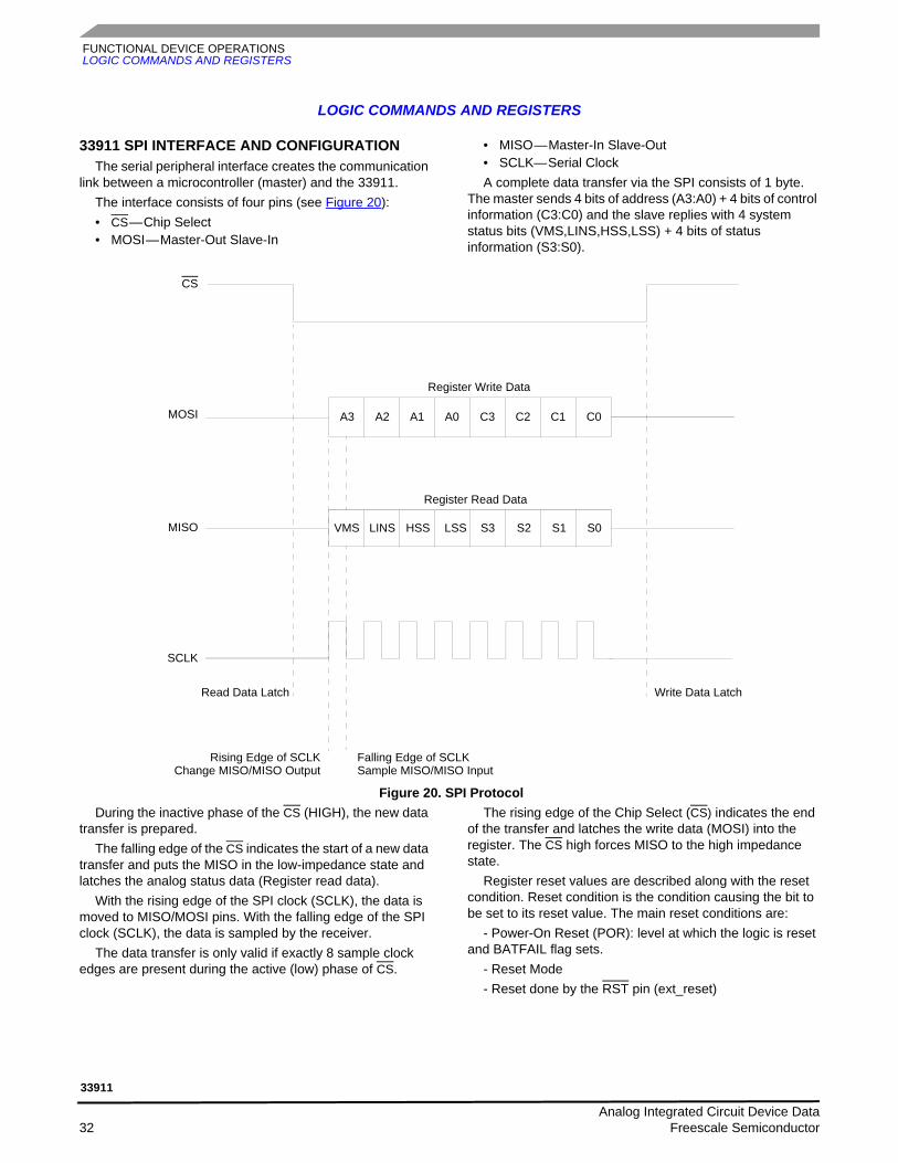
33911 SPI INTERFACE AND CONFIGURATIONThe serial peripheral interface creates the communication
link between a microcontroller (master) and the 33911.The interface consists of four pins (see Figure 20):• CS — Chip Select• MOSI — Master-Out Slave-In
• MISO — Master-In Slave-Out• SCLK— Serial ClockA complete data transfer via the SPI consists of 1 byte.
The master sends 4 bits of address (A3:A0) + 4 bits of control information (C3:C0) and the slave replies with 4 system status bits (VMS,LINS,HSS,LSS) + 4 bits of status information (S3:S0).
Figure 20. SPI ProtocolDuring the inactive phase of the CS (HIGH), the new data
transfer is prepared. The falling edge of the CS indicates the start of a new data
transfer and puts the MISO in the low-impedance state and latches the analog status data (Register read data).
With the rising edge of the SPI clock (SCLK), the data is moved to MISO/MOSI pins. With the falling edge of the SPI clock (SCLK), the data is sampled by the receiver.
The data transfer is only valid if exactly 8 sample clock edges are present during the active (low) phase of CS.
The rising edge of the Chip Select (CS) indicates the end of the transfer and latches the write data (MOSI) into the register. The CS high forces MISO to the high impedance state.
Register reset values are described along with the reset condition. Reset condition is the condition causing the bit to be set to its reset value. The main reset conditions are:
- Power-On Reset (POR): level at which the logic is reset and BATFAIL flag sets.
- Reset Mode- Reset done by the RST pin (ext_reset)
CS
MOSI
MISO
SCLK
A2 A1 A0 C3 C2 C1 C0A3
VMS LINS HSS LSS S3 S2 S1 S0
Read Data Latch
Rising Edge of SCLKChange MISO/MISO Output
Falling Edge of SCLKSample MISO/MISO Input
Write Data Latch
Register Write Data
Register Read Data
Analog Integrated Circuit Device Data 32 Freescale Semiconductor
33911
FUNCTIONAL DEVICE OPERATIONSLOGIC COMMANDS AND REGISTERS
SPI REGISTER OVERVIEW
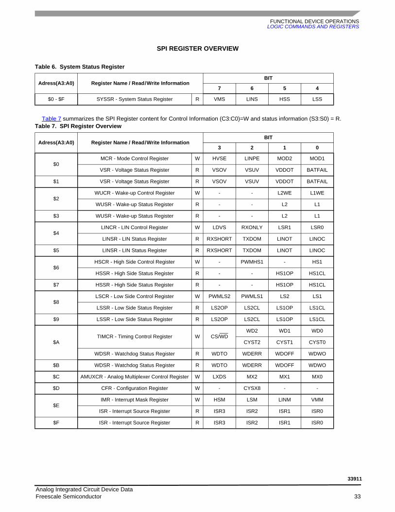
Table 7 summarizes the SPI Register content for Control Information (C3:C0)=W and status information (S3:S0) = R.
Table 6. System Status Register
Adress(A3:A0) Register Name / Read / Write InformationBIT
7 6 5 4
$0 - $F SYSSR - System Status Register R VMS LINS HSS LSS
Table 7. SPI Register Overview
Adress(A3:A0) Register Name / Read / Write InformationBIT
3 2 1 0
$0MCR - Mode Control Register W HVSE LINPE MOD2 MOD1
VSR - Voltage Status Register R VSOV VSUV VDDOT BATFAIL
$1 VSR - Voltage Status Register R VSOV VSUV VDDOT BATFAIL
$2WUCR - Wake-up Control Register W - - L2WE L1WE
WUSR - Wake-up Status Register R - - L2 L1
$3 WUSR - Wake-up Status Register R - - L2 L1
$4LINCR - LIN Control Register W LDVS RXONLY LSR1 LSR0
LINSR - LIN Status Register R RXSHORT TXDOM LINOT LINOC
$5 LINSR - LIN Status Register R RXSHORT TXDOM LINOT LINOC
$6HSCR - High Side Control Register W - PWMHS1 - HS1
HSSR - High Side Status Register R - - HS1OP HS1CL
$7 HSSR - High Side Status Register R - - HS1OP HS1CL
$8LSCR - Low Side Control Register W PWMLS2 PWMLS1 LS2 LS1
LSSR - Low Side Status Register R LS2OP LS2CL LS1OP LS1CL
$9 LSSR - Low Side Status Register R LS2OP LS2CL LS1OP LS1CL
$ATIMCR - Timing Control Register W CS/WD
WD2 WD1 WD0
CYST2 CYST1 CYST0
WDSR - Watchdog Status Register R WDTO WDERR WDOFF WDWO
$B WDSR - Watchdog Status Register R WDTO WDERR WDOFF WDWO
$C AMUXCR - Analog Multiplexer Control Register W LXDS MX2 MX1 MX0
$D CFR - Configuration Register W - CYSX8 - -
$EIMR - Interrupt Mask Register W HSM LSM LINM VMM
ISR - Interrupt Source Register R ISR3 ISR2 ISR1 ISR0
$F ISR - Interrupt Source Register R ISR3 ISR2 ISR1 ISR0
Analog Integrated Circuit Device Data Freescale Semiconductor 33
33911
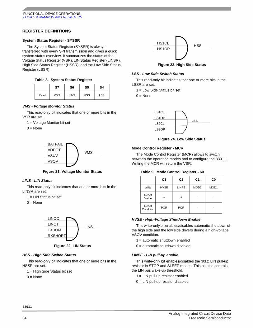
FUNCTIONAL DEVICE OPERATIONSLOGIC COMMANDS AND REGISTERS
REGISTER DEFINITIONS
System Status Register - SYSSRThe System Status Register (SYSSR) is always
transferred with every SPI transmission and gives a quick system status overview. It summarizes the status of the Voltage Status Register (VSR), LIN Status Register (LINSR), High Side Status Register (HSSR), and the Low Side Status Register (LSSR).
VMS - Voltage Monitor StatusThis read-only bit indicates that one or more bits in the
VSR are set.1 = Voltage Monitor bit set0 = None
Figure 21. Voltage Monitor Status
LINS - LIN StatusThis read-only bit indicates that one or more bits in the
LINSR are set.1 = LIN Status bit set0 = None
Figure 22. LIN Status
HSS - High Side Switch StatusThis read-only bit indicates that one or more bits in the
HSSR are set.1 = High Side Status bit set0 = None
Figure 23. High Side Status
LSS - Low Side Switch StatusThis read-only bit indicates that one or more bits in the
LSSR are set.1 = Low Side Status bit set0 = None
Figure 24. Low Side Status
Mode Control Register - MCRThe Mode Control Register (MCR) allows to switch
between the operation modes and to configure the 33911. Writing the MCR will return the VSR.
HVSE - High-Voltage Shutdown EnableThis write-only bit enables/disables automatic shutdown of
the high side and the low side drivers during a high-voltage VSOV condition.
1 = automatic shutdown enabled0 = automatic shutdown disabled
LINPE - LIN pull-up enable.This write-only bit enables/disables the 30kΩ LIN pull-up
resistor in STOP and SLEEP modes. This bit also controls the LIN bus wake-up threshold.
1 = LIN pull-up resistor enabled0 = LIN pull-up resistor disabled
Table 8. System Status Register
S7 S6 S5 S4
Read VMS LINS HSS LSS
VMS
BATFAILVDDOTVSUVVSOV
LINS
LINOCLINOTTXDOMRXSHORT
Table 9. Mode Control Register - $0
C3 C2 C1 C0
Write HVSE LINPE MOD2 MOD1
Reset Value 1 1 - -
Reset Condition POR POR - -
HSSHS1CLHS1OP
LS2OP
LS2CL
LS1OP
LS1CL
LSS
Analog Integrated Circuit Device Data 34 Freescale Semiconductor
33911
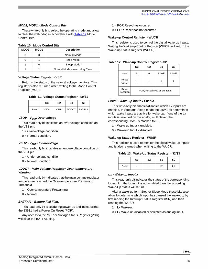
FUNCTIONAL DEVICE OPERATIONSLOGIC COMMANDS AND REGISTERS
MOD2, MOD1 - Mode Control BitsThese write-only bits select the operating mode and allow
to clear the watchdog in accordance with Table 12 Mode Control Bits.
Table 10. Mode Control Bits
Voltage Status Register - VSRReturns the status of the several voltage monitors. This
register is also returned when writing to the Mode Control Register (MCR).
VSOV - VSUP Over-voltageThis read-only bit indicates an over-voltage condition on
the VS1 pin.1 = Over-voltage condition.0 = Normal condition.
VSUV - VSUP Under-voltageThis read-only bit indicates an under-voltage condition on
the VS1 pin.1 = Under-voltage condition.0 = Normal condition.
VDDOT - Main Voltage Regulator Over-temperature Warning
This read-only bit indicates that the main voltage regulator temperature reached the Over-temperature Prewarning Threshold.
1 = Over-temperature Prewarning0 = Normal
BATFAIL - Battery Fail Flag.This read-only bit is set during power-up and indicates that
the 33911 had a Power On Reset (POR).Any access to the MCR or Voltage Status Register (VSR)
will clear the BATFAIL flag.
1 = POR Reset has occurred0 = POR Reset has not occurred
Wake-up Control Register - WUCRThis register is used to control the digital wake-up inputs.
Writing the Wake-up Control Register (WUCR) will return the Wake-up Status Register (WUSR).
Table 12. Wake-up Control Register - $2
LxWE - Wake-up Input x EnableThis write-only bit enables/disables which Lx inputs are
enabled. In Stop and Sleep mode the LxWE bit determines which wake inputs are active for wake-up. If one of the Lx inputs is selected on the analog multiplexer, the corresponding LxWE is masked to 0.
1 = Wake-up Input x enabled.0 = Wake-up Input x disabled.
Wake-up Status Register - WUSRThis register is used to monitor the digital wake-up inputs
and is also returned when writing to the WUCR.
Lx - Wake-up input xThis read-only bit indicates the status of the corresponding
Lx input. If the Lx input is not enabled then the according Wake-Up status will return 0.
After a wake-up form Stop or Sleep Mode these bits also allow to determine which input has caused the wake-up, by first reading the Interrupt Status Register (ISR) and then reading the WUSR.
1 = Lx Wake-up.0 = Lx Wake-up disabled or selected as analog input.
MOD2 MOD1 Description
0 0 Normal Mode
0 1 Stop Mode
1 0 Sleep Mode
1 1 Normal Mode + watchdog Clear
Table 11. Voltage Status Register - $0/$1
S3 S2 S1 S0
Read VSOV VSUV VDDOT BATFAIL
C3 C2 C1 C0
Write 0 0 L2WE L1WE
ResetValue
1 1 1 1
Reset Condition POR, Reset Mode or ext_reset
Table 13. Wake-Up Status Register - $2/$3
S3 S2 S1 S0
Read - - L2 L1
Analog Integrated Circuit Device Data Freescale Semiconductor 35
33911
FUNCTIONAL DEVICE OPERATIONSLOGIC COMMANDS AND REGISTERS
LIN Control Register - LINCRThis register controls the LIN physical interface block.
Writing the LIN Control Register (LINCR) returns the LIN Status Register (LINSR).
* LIN failure gone: if LIN failure (overtemp, TxD/RxD short) was set, the flag resets automatically when the failure is gone.
LDVS - LIN Dominant Voltage SelectThis write-only bit controls the LIN Dominant voltage:1 = LIN Dominant Voltage = VLIN_DOM_1 (1.7V typ)
0 = LIN Dominant Voltage = VLIN_DOM_0 (1.1V typ)
RXONLY - LIN Receiver Operation Only.This write-only bit controls the behavior of the LIN
transmitter.In Normal mode the activation of the RXONLY bit disables
the LIN transmitter. In case of a LIN error condition this bit is automatically set.
In Stop Mode this bit disables the LIN wake-up functionality and the RXD pin will reflect the state of the LIN bus.
1 = only LIN receiver active (Normal Mode) or LIN wake-up disabled (Stop Mode).
0 = LIN fully enabled.
LSRx - LIN Slew-RateThis write-only bit controls the LIN driver slew-rate in
accordance with Table 15.
Table 15. LIN Slew-Rate Control
LIN Status Register - LINSRThis register returns the status of the LIN physical
interface block and is also returned when writing to the LIN Control Register (LINCR).
RXSHORT - RXD Short-circuitThis read-only bit indicates a short-circuit condition on
RXD (shorted either to 5.0V or to Ground). The short-circuit delay must be 8µs worst case to be detected and to shutdown the driver. To clear this bit, it must be read after the condition is gone (transition detected on RXD). The LIN driver is automatically re-enabled once the condition is gone.
1 = RxD short-circuit condition.0 = None.
TXDOM - TXD Permanent DominantThis read-only bit signals the detection of a TXD pin stuck
at dominant (Ground) condition and the resultant shutdown in the LIN transmitter. This condition is detected after the TXD pin remains in dominant state for more than 1 second typical value.
To clear this bit, it must be read after TXD has gone high. The LIN driver is automatically re-enabled once TXD goes high.
1 = TXD stuck at dominant fault detected.0 = None.
LINOT - LIN Driver Over-temperature ShutdownThis read-only bit signals that the LIN transceiver was
shut-down due to over-temperature. The transmitter is automatically re-enabled after the over-temperature condition is gone and TXD is high. The LINOT bit is cleared after SPI read once the condition is gone.
1 = LIN over-temperature shutdown0 = None
LINOC - LIN Driver Over-current ShutdownThis read-only bit signals an over-current condition
occurred on the LIN pin. The LIN driver is not shut down but an IRQ is generated. To clear this bit, it must be read after the condition is gone.
1 = LIN over-current shutdown0 = None
Table 14. LIN Control Register - $4
C3 C2 C1 C0
Write LDVS RXONLY LSR1 LSR0
Reset Value 0 0 0 0
Reset Condition
POR, Reset Mode or ext_reset
POR, Reset Mode, ext_reset
or LIN failure gone*
POR
LSR1 LSR0 Description
0 0 Normal Slew-Rate (up to 20kb/s)
0 1 Slow Slew-Rate (up to 10kb/s)
1 0 Fast Slew-Rate (up to 100kb/s)
1 1 Reserved
Table 16. LIN Status Register - $4/$5
S3 S2 S1 S0
Read RXSHORT TXDOM LINOT LINOC
Analog Integrated Circuit Device Data 36 Freescale Semiconductor
33911
FUNCTIONAL DEVICE OPERATIONSLOGIC COMMANDS AND REGISTERS
High Side Control Register - HSCRThis register controls the operation of the high side driver.
Writing to this register returns the High Side Status Register (HSSR).
PWMHS1 - PWM Input Control Enable.This write-only bit enables/disables the PWMIN input pin
to control the high side switch. The high side switch must be enabled (HS1 bit).
1 = PWMIN input controls HS1 output.0 = HS1 is controlled only by SPI.
HS1 - High Side Switch Control.This write-only bit enables/disables the high side switch.1 = HS1 switch on.0 = HS1 switch off.
High Side Status Register - HSSRThis register returns the status of the high side switch and
is also returned when writing to the High Side Control Register (HSCR).
High Side thermal shutdown A thermal shutdown of the high side drivers is indicated by
setting the HS1OP and HS1CL bits simultaneously.
HS1OP - High Side Switch Open-Load DetectionThis read-only bit signals that the high side switch is
conducting current below a certain threshold indicating possible load disconnection.
1 = HS1 Open Load detected (or thermal shutdown)0 = Normal
HS1CL - High Side Current LimitationThis read-only bit indicates that the high side switch is
operating in current limitation mode.1 = HS1 in current limitation (or thermal shutdown)0 = Normal
Low Side Control Register - LSCRThis register controls the operation of the low side drivers.
Writing the Low Side Control Register (LSCR) will also return the Low Side Status Register (LSSR).
PWMLx - PWM input control enable.This write-only bit enables/disables the PWMIN input pin
to control the respective low side switch. The corresponding low side switch must be enabled (LSx bit).
1 = PWMIN input controls LSx.0 = LSx is controlled only by SPI.
LSx - LSx switch control.This write-only bit enables/disables the corresponding low
side switch.1 = LSx switch on.0 = LSx switch off.
Low Side Status Register - LSSRThis register returns the status of the low side switches
and is also returned when writing to the LSCR.
Low Side thermal shutdown A thermal shutdown of the low side drivers is indicated by
setting all LSxOP and LSxCL bits simultaneously.
LSxOP - Low Side Switch Open-Load DetectionThis read-only bit signals that the low side switches are
conducting current below a certain threshold indicating possible load disconnection.
1 = LSx Open-load detected (or thermal shutdown)0 = Normal
LSxCL - Low Side Current LimitationThis read-only bit indicates that the respective low side
switch is operating in current limitation mode.1 = LSx in current limitation (or thermal shutdown)0 = Normal
Table 17. High Side Control Register - $6
C3 C2 C1 C0
Write 0 PWMHS1 0 HS1
Reset Value 0 0 0 0
Reset Condition POR POR, Reset Mode, ext_reset, HS1
overtemp or (VSOV & HVSE)
Table 18. High Side Status Register - $6/$7
S3 S2 S1 S0
Read - - HS1OP HS1CL
Table 19. Low Side Control Register - $8
C3 C2 C1 C0
Write PWMLS2 PWMLS1 LS2 LS1
Reset Value 0 0 0 0
Reset Condition POR POR, Reset Mode, ext_reset, LSx
overtemp or (VSOV & HVSE)
Table 20. Low Side Status Register - $8/$9
C3 C2 C1 C0
Read LS2OP LS2CL LS1OP LS1CL
Analog Integrated Circuit Device Data Freescale Semiconductor 37
33911
FUNCTIONAL DEVICE OPERATIONSLOGIC COMMANDS AND REGISTERS
Timing Control Register - TIMCRThis register is a double purpose register which allows to
configure the watchdog and the cyclic sense periods. Writing to the Timing Control Register (TIMCR) will also return the Watchdog Status Register (WDSR).
CS/WD - Cyclic Sense or Watchdog prescaler select.This write-only bit selects which prescaler is being written
to, the Cyclic Sense prescaler or the watchdog prescaler.1 = Cyclic Sense Prescaler selected0 = watchdog Prescaler select
WDx - Watchdog PrescalerThis write-only bits selects the divider for the watchdog
prescaler and therefore selects the watchdog period in accordance with Table 22. This configuration is valid only if windowing watchdog is active.
Table 22. Watchdog Prescaler
CYSTx - Cyclic Sense Period Prescaler SelectThis write-only bits selects the interval for the wake-up
cyclic sensing together with the bit CYSX8 in the Configuration Register (CFR) (see page 39).
This option is only active if the high side switch is enabled when entering in Stop or Sleep Mode. Otherwise a timed wake-up is performed after the period shown in Table 23.
Table 23. Cyclic Sense Interval
Watchdog Status Register - WDSRThis register returns the watchdog status information and
is also returned when writing to the TIMCR.
WDTO - Watchdog TimeoutThis read-only bit signals the last reset was caused by
either a watchdog timeout or by an attempt to clear the watchdog within the window closed.
Any access to this register or the TIMCR will clear the WDTO bit.
1 = Last reset caused by watchdog timeout0 = None
Table 21. Timing Control Register - $A
C3 C2 C1 C0
Write CS/WDWD2 WD1 WD0
CYST2 CYST1 CYST0
Reset Value - 0 0 0
Reset Condition - POR
WD2 WD1 WD0 Prescaler Divider
0 0 0 1
0 0 1 2
0 1 0 4
0 1 1 6
1 0 0 8
1 0 1 10
1 1 0 12
1 1 1 14
CYSX8(59) CYST2 CYST1 CYST0 Interval
X 0 0 0 No cyclic sense
0 0 0 1 20ms
0 0 1 0 40ms
0 0 1 1 60ms
0 1 0 0 80ms
0 1 0 1 100ms
0 1 1 0 120ms
0 1 1 1 140ms
1 0 0 1 160ms
1 0 1 0 320ms
1 0 1 1 480ms
1 1 0 0 640ms
1 1 0 1 800ms
1 1 1 0 960ms
1 1 1 1 1120ms
Notes59. bit CYSX8 is located in Configuration Register (CFR)
Table 24. Watchdog Status Register - $A/$B
S3 S2 S1 S0
Read WDTO WDERR WDOFF WDWO
Analog Integrated Circuit Device Data 38 Freescale Semiconductor
33911
FUNCTIONAL DEVICE OPERATIONSLOGIC COMMANDS AND REGISTERS
WDERR - Watchdog ErrorThis read-only bit signals the detection of a missing
watchdog resistor. In this condition the watchdog is using the internal, lower precision timebase. The Windowing function is disabled.
1 = WDCONF pin resistor missing0 = WDCONF pin resistor not floating
WDOFF - Watchdog OffThis read-only bit signals that the watchdog pin connected
to Ground and therefore disabled. In this case watchdog timeouts are disabled and the device automatically enters Normal Mode out of Reset. This might be necessary for software debugging and for programming the Flash memory.
1 = Watchdog is disabled0 = Watchdog is enabled
WDWO - Watchdog Window OpenThis read-only bit signals when the watchdog window is
open for clears. The purpose of this bit is for testing. Should be ignored in case WDERR is High.
1 = Watchdog window open0 = Watchdog window closed
Analog Multiplexer Control Register - MUXCRThis register controls the analog multiplexer and selects
the divider ration for the Lx input divider.
LXDS - Lx Analog Input Divider SelectThis write-only bit selects the resistor divider for the Lx
analog inputs. Voltage is internally clamped to VDD.0 = Lx Analog divider: 11 = Lx Analog divider: 3.6 (typ.)
MXx - Analog Multiplexer Input SelectThese write-only bits selects which analog input is
multiplexed to the ADOUT0 pin according to Table 26.When disabled or when in Stop or Sleep Mode, the output
buffer is not powered and the ADOUT0 output is left floating to achieve lower current consumption.
Table 26. Analog Multiplexer Channel Select
Configuration Register - CFRThis register controls the cyclic sense timing multiplier.
CYSX8 - Cyclic Sense Timing x 8.This write-only bit influences the cyclic sense period as
shown in Table 23.1 = Multiplier enabled0 = None
Table 25. Analog Multiplexer Control Register -$C
C3 C2 C1 C0
Write LXDS MX2 MX1 MX0
Reset Value 1 0 0 0
Reset Condition POR POR, Reset Mode or ext_reset
MX2 MX1 MX0 Meaning
0 0 0 Disabled
0 0 1 Reserved
0 1 0 Die Temperature Sensor
0 1 1 VSENSE input
1 0 0 L1 input
1 0 1 L2 input
1 1 0 Reserved
1 1 1 Reserved
Table 27. Configuration Register - $D
C3 C2 C1 C0
Write 0 CYSX8 0 0
Reset Value 0 0 0 0
Reset Condition
POR, Reset Mode or ext_reset
POR POR POR
Analog Integrated Circuit Device Data Freescale Semiconductor 39
33911
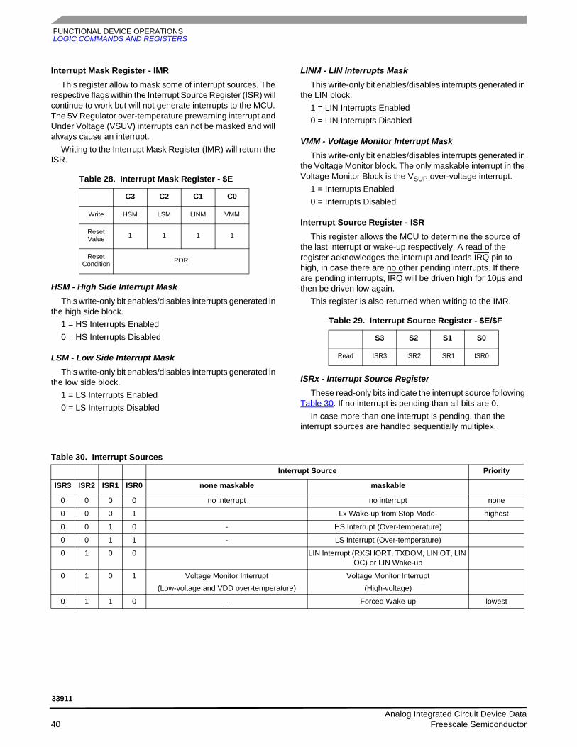
FUNCTIONAL DEVICE OPERATIONSLOGIC COMMANDS AND REGISTERS
Interrupt Mask Register - IMRThis register allow to mask some of interrupt sources. The
respective flags within the Interrupt Source Register (ISR) will continue to work but will not generate interrupts to the MCU. The 5V Regulator over-temperature prewarning interrupt and Under Voltage (VSUV) interrupts can not be masked and will always cause an interrupt.
Writing to the Interrupt Mask Register (IMR) will return the ISR.
HSM - High Side Interrupt MaskThis write-only bit enables/disables interrupts generated in
the high side block.1 = HS Interrupts Enabled0 = HS Interrupts Disabled
LSM - Low Side Interrupt MaskThis write-only bit enables/disables interrupts generated in
the low side block.1 = LS Interrupts Enabled0 = LS Interrupts Disabled
LINM - LIN Interrupts MaskThis write-only bit enables/disables interrupts generated in
the LIN block.1 = LIN Interrupts Enabled0 = LIN Interrupts Disabled
VMM - Voltage Monitor Interrupt MaskThis write-only bit enables/disables interrupts generated in
the Voltage Monitor block. The only maskable interrupt in the Voltage Monitor Block is the VSUP over-voltage interrupt.
1 = Interrupts Enabled0 = Interrupts Disabled
Interrupt Source Register - ISRThis register allows the MCU to determine the source of
the last interrupt or wake-up respectively. A read of the register acknowledges the interrupt and leads IRQ pin to high, in case there are no other pending interrupts. If there are pending interrupts, IRQ will be driven high for 10µs and then be driven low again.
This register is also returned when writing to the IMR.
ISRx - Interrupt Source RegisterThese read-only bits indicate the interrupt source following
Table 30. If no interrupt is pending than all bits are 0.In case more than one interrupt is pending, than the
interrupt sources are handled sequentially multiplex.
Table 30. Interrupt Sources
Table 28. Interrupt Mask Register - $E
C3 C2 C1 C0
Write HSM LSM LINM VMM
Reset Value 1 1 1 1
Reset Condition POR
Table 29. Interrupt Source Register - $E/$F
S3 S2 S1 S0
Read ISR3 ISR2 ISR1 ISR0
Interrupt Source Priority
ISR3 ISR2 ISR1 ISR0 none maskable maskable
0 0 0 0 no interrupt no interrupt none
0 0 0 1 Lx Wake-up from Stop Mode- highest
0 0 1 0 - HS Interrupt (Over-temperature)
0 0 1 1 - LS Interrupt (Over-temperature)
0 1 0 0 LIN Interrupt (RXSHORT, TXDOM, LIN OT, LIN OC) or LIN Wake-up
0 1 0 1 Voltage Monitor Interrupt(Low-voltage and VDD over-temperature)
Voltage Monitor Interrupt(High-voltage)
0 1 1 0 - Forced Wake-up lowest
Analog Integrated Circuit Device Data 40 Freescale Semiconductor
33911
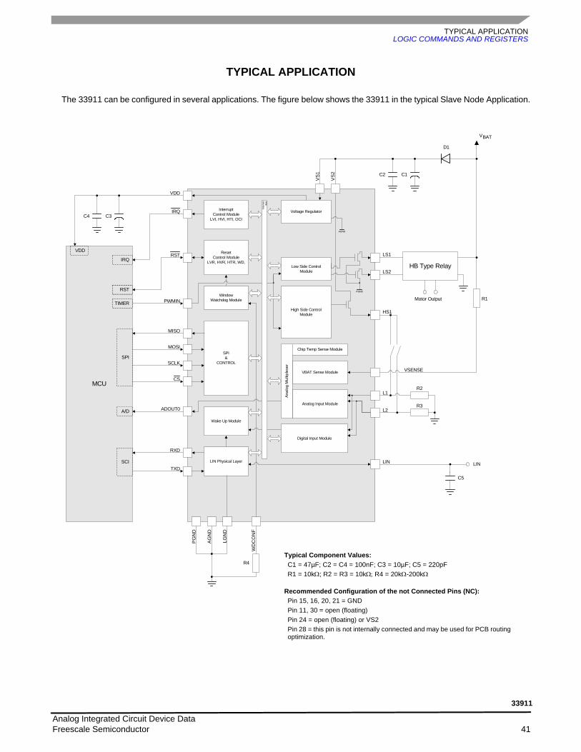
TYPICAL APPLICATIONLOGIC COMMANDS AND REGISTERS
TYPICAL APPLICATION
The 33911 can be configured in several applications. The figure below shows the 33911 in the typical Slave Node Application.
Voltage Regulator
SPI&
CONTROL
ResetControl Module
LVR, HVR, HTR, WD,
WindowWatchdog Module
LIN Physical Layer
VS2
HS1
LS2
VSENSE
Analog Input Module
Digital Input Module
LIN
RXD
ADOUT0
SCLK
MOSI
MISO
TXD
CS
Wake Up Module
InterruptControl Module
LVI, HVI, HTI, OCI
Low Side Control Module
VBAT Sense Module
Ana
log
Mul
tiple
xer
L2
L1
LS1
PGND
WD
CO
NF
Chip Temp Sense Module
PWMIN
High Side Control Module
LGN
D
Inte
rnal
Bus
MCU
RST
IRQA
GN
D
PG
ND
VS1
AGND
VDD
A/D
SCI
SPI
TIMER
RST
VDD
IRQ
C4 C3
R4
C2 C1
D1
V
R1
C5
LIN
R2
R3
HB Type Relay
Motor Output
BAT
Typical Component Values:C1 = 47µF; C2 = C4 = 100nF; C3 = 10µF; C5 = 220pFR1 = 10kΩ; R2 = R3 = 10kΩ; R4 = 20kΩ-200kΩ
Recommended Configuration of the not Connected Pins (NC):Pin 15, 16, 20, 21 = GNDPin 11, 30 = open (floating)Pin 24 = open (floating) or VS2Pin 28 = this pin is not internally connected and may be used for PCB routing optimization.
Analog Integrated Circuit Device Data Freescale Semiconductor 41
33911
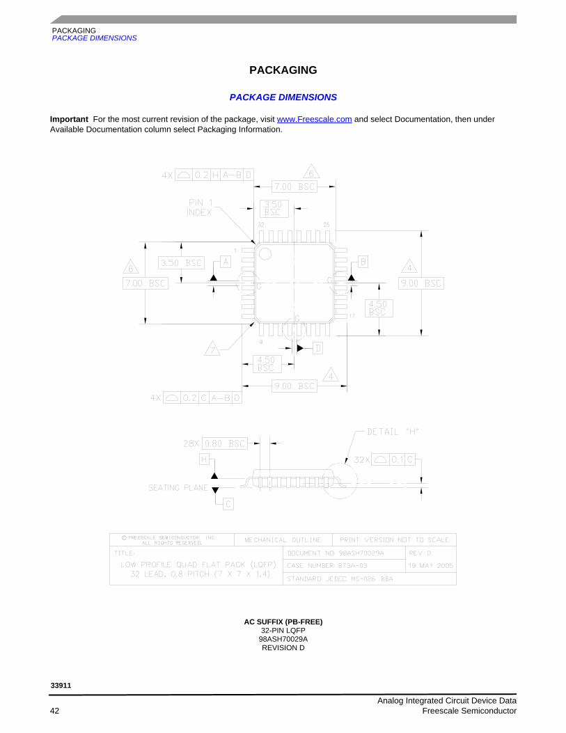
PACKAGINGPACKAGE DIMENSIONS
PACKAGING
PACKAGE DIMENSIONS
Important For the most current revision of the package, visit www.Freescale.com and select Documentation, then under Available Documentation column select Packaging Information.
AC SUFFIX (PB-FREE)32-PIN LQFP
98ASH70029AREVISION D
Analog Integrated Circuit Device Data 42 Freescale Semiconductor
33911
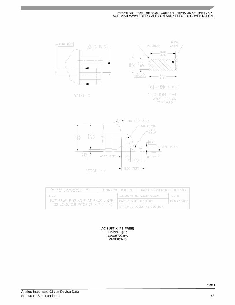
IMPORTANT FOR THE MOST CURRENT REVISION OF THE PACK-AGE, VISIT WWW.FREESCALE.COM AND SELECT DOCUMENTATION,
AC SUFFIX (PB-FREE)32-PIN LQFP
98ASH70029AREVISION D
Analog Integrated Circuit Device Data Freescale Semiconductor 43
33911
REVISION HISTORYPACKAGE DIMENSIONS
REVISION HISTORY
Revision Date Description of Changes
3.0 9/2007 • Initial Release
4.0 2/2008 • Changed Functional Block Diagram on page 22.• Corrected typo for Outline drawing number (98A...).
Analog Integrated Circuit Device Data 44 Freescale Semiconductor
33911
MC33911Rev. 4.02/2008
Information in this document is provided solely to enable system and software implementers to use Freescale Semiconductor products. There are no express or implied copyright licenses granted hereunder to design or fabricate any integrated circuits or integrated circuits based on the information in this document.
Freescale Semiconductor reserves the right to make changes without further notice to any products herein. Freescale Semiconductor makes no warranty, representation or guarantee regarding the suitability of its products for any particular purpose, nor does Freescale Semiconductor assume any liability arising out of the application or use of any product or circuit, and specifically disclaims any and all liability, including without limitation consequential or incidental damages. “Typical” parameters that may be provided in Freescale Semiconductor data sheets and/or specifications can and do vary in different applications and actual performance may vary over time. All operating parameters, including “Typicals”, must be validated for each customer application by customer’s technical experts. Freescale Semiconductor does not convey any license under its patent rights nor the rights of others. Freescale Semiconductor products are not designed, intended, or authorized for use as components in systems intended for surgical implant into the body, or other applications intended to support or sustain life, or for any other application in which the failure of the Freescale Semiconductor product could create a situation where personal injury or death may occur. Should Buyer purchase or use Freescale Semiconductor products for any such unintended or unauthorized application, Buyer shall indemnify and hold Freescale Semiconductor and its officers, employees, subsidiaries, affiliates, and distributors harmless against all claims, costs, damages, and expenses, and reasonable attorney fees arising out of, directly or indirectly, any claim of personal injury or death associated with such unintended or unauthorized use, even if such claim alleges that Freescale Semiconductor was negligent regarding the design or manufacture of the part.
Freescale™ and the Freescale logo are trademarks of Freescale Semiconductor, Inc. All other product or service names are the property of their respective owners.© Freescale Semiconductor, Inc., 2007. All rights reserved.
How to Reach Us:
Home Page:www.freescale.com
Web Support:http://www.freescale.com/support
USA/Europe or Locations Not Listed:Freescale Semiconductor, Inc.Technical Information Center, EL5162100 East Elliot Road Tempe, Arizona 85284 +1-800-521-6274 or +1-480-768-2130www.freescale.com/support
Europe, Middle East, and Africa:Freescale Halbleiter Deutschland GmbHTechnical Information CenterSchatzbogen 781829 Muenchen, Germany+44 1296 380 456 (English)+46 8 52200080 (English)+49 89 92103 559 (German)+33 1 69 35 48 48 (French)www.freescale.com/support
Japan:Freescale Semiconductor Japan Ltd. Headquarters ARCO Tower 15F 1-8-1, Shimo-Meguro, Meguro-ku, Tokyo 153-0064Japan0120 191014 or +81 3 5437 [email protected]
Asia/Pacific:Freescale Semiconductor Hong Kong Ltd.Technical Information Center 2 Dai King Street Tai Po Industrial Estate Tai Po, N.T., Hong Kong +800 2666 [email protected]
For Literature Requests Only:Freescale Semiconductor Literature Distribution CenterP.O. Box 5405Denver, Colorado 802171-800-441-2447 or 303-675-2140Fax: [email protected]