Embed Size (px)
Citation preview

Evaluation Board User Guide UG-040
One Technology Way • P.O. Box 9106 • Norwood, MA 02062-9106, U.S.A. • Tel: 781.329.4700 • Fax: 781.461.3113 • www.analog.com
Evaluating the AD1937/AD1939 Four ADC/Eight DAC with PLL 192 kHz, 24-Bit Codec
PLEASE SEE THE LAST PAGE FOR AN IMPORTANT WARNING AND LEGAL TERMS AND CONDITIONS. Rev. 0 | Page 1 of 32
EVAL-AD1937AZ/EVAL-AD1939AZ PACKAGE CONTENTS AD1937/AD1939 evaluation board USBi control interface board USB cable
OTHER SUPPORTING DOCUMENTATION AD1937 data sheet AD1939 data sheet
EVALUATION BOARD OVERVIEW This document explains the design and setup of the evaluation board for the AD1937 and AD1939. The evaluation board must be connected to an external ±12 V dc power supply and ground. On-board regulators derive 5 V and 3.3 V supplies for the AD1937/AD1939. The AD1937/AD1939 can be controlled
through an SPI or I2C interface. A small external interface board, EVAL-ADUSB2EBZ (also called USBi), connects to a PC USB port and provides I2C and SPI access to the evaluation board through a ribbon cable. A graphical user interface (GUI) program is provided for easy programming of the chip in a Microsoft® Windows® PC environment. The evaluation board allows demonstration and performance testing of most AD1937/AD1939 features, including four ADCs and eight DACs, as well as the digital audio ports.
Additional analog circuitry (ADC input filters, DAC output filter/buffer) and digital interfaces such as S/PDIF are provided to ease product evaluation.
All analog audio interfaces are accessible with stereo audio, 3.5 mm TRS connectors.
FUNCTIONAL BLOCK DIAGRAM
0841
1-00
1Pb
a
SERIAL AUDIOINTERFACES
CLOCK ANDDATA ROUTING
AD1939VOLTREG
AD1939
MCLK ROUTING
ANALOGAUDIO
DAC 3 AND DAC 4
DAC 1 AND DAC 2
ANALOGAUDIO
ANALOGAUDIO
ADC 1 AND ADC 2
SPI
POWER SUPPLY
CONTROLINTERFACE
S/PDIFINTERFACE
LRCLK, BCLK, SDATA
Figure 1.

UG-040 Evaluation Board User Guide
Rev. 0 | Page 2 of 32
TABLE OF CONTENTS EVAL-AD1937AZ/EVAL-AD1939AZ Package Contents ........... 1
Other Supporting Documentation ................................................. 1
Evaluation Board Overview ............................................................ 1
Functional Block Diagram .............................................................. 1
Revision History ............................................................................... 2
Setting Up the Evaluation Board .................................................... 3
Standalone Mode .......................................................................... 3
SPI and I2C Control ...................................................................... 3
Automated Register Window Builder Software Installation .. 3
Hardware Setup—USBi ............................................................... 3
Powering the Board .......................................................................4
Setting Up the Master Clock (MCLK) ........................................4
Configuring the PLL Filter ...........................................................5
Connecting Audio Cables ............................................................6
Switch and Jumper Settings .........................................................6
Rotary and DIP Switch Settings ......................................................8
Schematics and Artwork ............................................................... 10
CPLD Code ..................................................................................... 21
Ordering Information .................................................................... 27
Bill of Materials ........................................................................... 27
REVISION HISTORY 2/10—Revision 0: Initial Version

Evaluation Board User Guide UG-040
Rev. 0 | Page 3 of 32
SETTING UP THE EVALUATION BOARD STANDALONE MODE It is possible to run the board and the AD1937/AD1939 codec in standalone mode, which fixes the functionality of the AD1937/AD1939 into the I2S data format, running at 256 × fS (default register condition). The ADC BCLK and LRCLK ports are flipped between slave and master (input and output) by tying SDA/COUT (Pin 31) to low or high. This is accomplished by moving the J5 jumper to either 0 or SDA/1 (see Figure 2 and Figure 3).
0841
1-00
2
0SD
A/1
CO
UT 0 1
CIN
J6 J8J7
ADDR1ADDR0
J5
0SC
LC
CLK
0 1C
LATC
H
Figure 2. Standalone Slave Mode
0841
1-00
3
0SD
A/1
CO
UT 0 1
CIN
J6 J8J7
ADDR1ADDR0
J5
0SC
LC
CLK
0 1C
LATC
H
Figure 3. Standalone Master Mode
With the control jumpers set to standalone slave mode, all of S2 and S3 set to off, and both mode switches (S4 and S5) set to 0. The S/PDIF receiver is the LRCLK, BCLK, and SDATA source. The default MCLK jumper setting routes MCLK from the S/PDIF receiver to the AD1937/AD1939. With a valid S/PDIF data stream connected to a selected S/PDIF input port, the board passes audio from the S/PDIF port to all four stereo outputs and from Stereo IN1 to the S/PDIF output ports. IN2 can be selected by changing S3, Position 8, to on. Other serial audio clock and data routing configurations are described in the Switch and Jumper Settings section.
SPI AND I2C CONTROL The evaluation board can be configured for interactive control of the registers in the AD1937/AD1939 by connecting the SPI or I2C port to the USBi. SPI and I2C jumper settings are shown in Figure 4 and Figure 5. All part variations are SPI (for the AD1939). Note that the Automated Register Window Builder software controls the AD1937 (I2C) only when the ADDR jumpers are set to 00 and the correct .xml file is loaded.
0841
1-00
4
0SD
A/1
CO
UT 0 1
CIN
J6 J8J7
ADDR1ADDR0
J5
0SC
LC
CLK
0 1C
LATC
H
Figure 4. SPI Control
0841
1-00
5
0SD
A/1
CO
UT 0 1
CIN
J6 J8J7
ADDR1ADDR0
J5
0SC
LC
CLK
0 1C
LATC
H
Figure 5. I2C Control
The Automated Register Window Builder controls the AD1937/AD1939 and is available at www.analog.com/AD1937 or www.analog.com/AD1939.
AUTOMATED REGISTER WINDOW BUILDER SOFTWARE INSTALLATION The Automated Register Window Builder is a program that launches a graphical user interface for direct, live control of the AD1937/AD1939 registers. The GUI content for a part is defined in a part-specific . xml file; these files are included in the software installation. To install the Automated Register Window Builder software, follow these steps:
1. At www.analog.com/AD1937 or www.analog.com/AD1939, find the Resources & Tools list.
2. In the list, find Evaluation Boards & Development Kits and click Evaluation Boards/Tools to open the provided ARWBvXX.zip file.
3. Double-click the provided .msi file to extract the files to an empty folder on your PC.
4. Then double-click setup.exe and follow the prompts to install the Automated Register Window Builder. A computer restart is not required.
5. Copy the .xml file for the AD1937/AD1939 from the extraction folder into the C:\Program Files\Analog Devices Inc\AutomatedRegWin folder, if it does not appear in the folder after installation.
HARDWARE SETUP—USBi To set up the USBi hardware, follow these steps:
1. Plug the USBi ribbon cable into the J1 header. 2. Connect the USB cable to your computer and to the USBi. 3. When prompted for drivers, follow these steps:
a. Choose Install from a list or a specific location. b. Choose Search for the best driver in these locations. c. Check the box Include this location in the search. d. Find the USBi driver in C:\Program Files\Analog
Devices Inc\AutomatedRegWin\USB drivers. e. Click Next. f. If prompted to choose a driver, select CyUSB.sys. g. If the PC is running Windows XP and you receive a
message that the software has not passed Windows logo testing, click Continue Anyway.

UG-040 Evaluation Board User Guide
Rev. 0 | Page 4 of 32
You can now open the Automated Register Window Builder application and load the file for the part onto your evaluation board.
POWERING THE BOARD The AD1937/AD1939 evaluation board requires power supply input of ±12 V dc and ground to the three binding posts; +12 V draws ~250 mA, and −12 V draws ~100 mA. The on-board regulators provide two 3.3 V rails and one 5.0 V rail. The 3.3 V rails supply AVDD and DVDD for the AD1937/AD1939; DVDD also supplies power for the peripheral active components on the board. The 5.0 V rail provides voltage only to the AD1937/ AD1939 internal regulator, which consists of a PNP pass tran-sistor and a few passive components. The PNP is driven into 3.3 V regulation by the VDRIVE pin of the AD1937/AD1939, with the VSUPPLY and VSENSE pins acting as power and feedback for the regulator. An appropriate sized PNP can supply 3.3 V to the AVDD and DVDD pins of the AD1937/AD1939. The jumper blocks are shown in Figure 6 and Figure 7.
0841
1-00
6
MAIN REGSC122
R117
C96
Q1
AVD
D2
AVD
D1
R10
2C
97
DVD
D
193X REG
193X
REG
JP6 JP7
JP15
JP5
ENABLEDISABLE
Figure 6. AD1939 Main Regulators Active
0841
1-00
7
MAIN REGSC122
R117
C96
Q1
AVD
D2
AVD
D1
R10
2C
97
DVD
D
193X REG
193X
REG
JP6 JP7
JP15
JP5
ENABLEDISABLE
Figure 7. AD1939 Internal Regulator Active
The first step in using the AD1937/AD1939 internal regulator is to provide power to the regulator circuit by moving the AD1937/ AD1939 REG jumper from DISABLE to ENABLE, as shown in Figure 7. Three discrete jumpers allow the AD1937/AD1939 to be run from either the main AVDD and DVDD regulators or the AD1937/AD1939 internal regulator. These jumpers also allow measurement of current drawn by the individual sections of the AD1937/AD1939. The only components on the AD1937/ AD1939 side of the jumper are the AD1937/AD1939 and the supply decoupling capacitors.
SETTING UP THE MASTER CLOCK (MCLK) The AD1937/AD1939 evaluation board has a series of jumpers that give the user great flexibility in the MCLK clock source of the AD1937/AD1939. MCLK can come from six different sources: passive crystal, active oscillator, external clock in, S/PDIF receiver, and two header connections. Note that the complex programmable logic device (CPLD) on the board must have a valid clock source; the frequency is not critical. These jumper blocks can assign a clock to the CPLD as well. Most applications of the board use MCLK from either the S/PDIF receiver or one of the header (HDR) inputs. Figure 8 to Figure 10 show the on-board active oscillator disabled so that it does not interfere with the selected clock. The clock feed to the CPLD comes directly from the clock source.
Note that, if the HDR connectors are to be driven with MCLK from a source on the evaluation board, SW2 and/or SW3 must be switched from the IN position to the OUT position.
0841
1-00
8
JP31HDR1
JP30HDR2
JP298416
JP28CLK
JP24
OSC
R15
5
R15
6
C15
4
C15
3
MC
LKI
XTA
L MCLKOXTAL
R16
6
R17
8
MC
LKI B
US
MC
LKO
BU
S
JP27HDR1
JP25HDR2
JP23CPLD
OSC DISABLE
193X_MCLKIDISABLE
EXT
EXT CLK IN
193X_MCLKO
1938_MCLKIR160
R167
R169
R172
R174 R175
C168C170
JP22
C158L7
JP19
JP18 JP20 C147
U21
U18
U22
Y1
J23
J22
Figure 8. S/PDIF Receiver as MCLK Master; the AD1939 and CPLD as Slaves
0841
1-00
9
JP31HDR1
JP30HDR2
JP298416
JP28CLK
JP24
OSC
R15
5
R15
6
C15
4
C15
3
MC
LKI
XTA
L MCLKOXTAL
R16
6
R17
8
MC
LKI B
US
MC
LKO
BU
S
JP27HDR1
JP25HDR2
JP23CPLD
OSC DISABLE
193X_MCLKIDISABLE
EXT
EXT CLK IN
193X_MCLKO
1938_MCLKIR160
R167
R169
R172
R174 R175
C168C170
JP22
C158L7
JP19
JP18 JP20 C147
U21
U18
U22
Y1
J23
J22
Figure 9. HDR1 as MCLK Master; the AD1939, CPLD, and HDR2 as Slaves
Evaluation Board User Guide UG-040
Rev. 0 | Page 5 of 32
0841
1-01
0
JP31HDR1
JP30HDR2
JP298416
JP28CLK
JP24
OSC
R15
5
R15
6
C15
4
C15
3
MC
LKI
XTA
L MCLKOXTAL
R16
6
R17
8
MC
LKI B
US
MC
LKO
BU
S
JP27HDR1
JP25HDR2
JP23CPLD
OSC DISABLE
193X_MCLKIDISABLE
EXT
EXT CLK IN
193X_MCLKO
1938_MCLKIR160
R167
R169
R172
R174 R175
C168C170
JP22
C158L7
JP19
JP18 JP20 C147
U21
U18
U22
Y1
J23
J22
Figure 10. External Clock In as Master; the AD1939 and CPLD as Slaves
08
411-
011
JP31HDR1
JP30HDR2
JP298416
JP28CLK
JP24
OSC
R15
5
R15
6
C15
4
C15
3
MC
LKI
XTA
L MCLKOXTAL
R16
6
R17
8
MC
LKI B
US
MC
LKO
BU
S
JP27HDR1
JP25HDR2
JP23CPLD
OSC DISABLE
193X_MCLKIDISABLE
EXT
EXT CLK IN
193X_MCLKO
1938_MCLKIR160
R167
R169
R172
R174 R175
C168C170
JP22
C158L7
JP19
JP18 JP20 C147
U21
U18
U22
Y1
J23
J22
Figure 11. Active On-Board Oscillator as Master; the AD1939 and
CPLD as Slaves
The MCLK configurations shown in Figure 12 and Figure 13 use the AD1937/AD1939 MCLKO port to drive the CPLD and, possibly, the HDRs. The passive crystal runs the AD1937/AD1939 at 12.288 MHz. Figure 13 shows the MCLKI shut off; this is the case when the PLL is set to lock to LRCLK instead of to MCLK.
0841
1-01
2
JP31HDR1
JP30HDR2
JP298416
JP28CLK
JP24
OSC
R15
5
R15
6
C15
4
C15
3
MC
LKI
XTA
L MCLKOXTAL
R16
6
R17
8
MC
LKI B
US
MC
LKO
BU
S
JP27HDR1
JP25HDR2
JP23CPLD
OSC DISABLE
193X_MCLKIDISABLE
EXT
EXT CLK IN
193X_MCLKO
1938_MCLKIR160
R167
R169
R172
R174 R175
C168C170
JP22
C158L7
JP19
JP18 JP20 C147
U21
U18
U22
Y1
J23
J22
Figure 12. Passive Crystal; the AD1939 Is Master and the CPLD Is Slave from
the MCLKO Port
0841
1-01
3
JP31HDR1
JP30HDR2
JP298416
JP28CLK
JP24
OSC
R15
5
R15
6
C15
4
C15
3
MC
LKI
XTA
L MCLKOXTAL
R16
6
R17
8
MC
LKI B
US
MC
LKO
BU
S
JP27HDR1
JP25HDR2
JP23CPLD
OSC DISABLE
193X_MCLKIDISABLE
EXT
EXT CLK IN
193X_MCLKO
1938_MCLKIR160
R167
R169
R172
R174 R175
C168C170
JP22
C158L7
JP19
JP18 JP20 C147
U21
U18
U22
Y1
J23
J22
Figure 13. LRCLK Is the Master Clock Using the PLL; MCLKI Is Disabled, and
CPLD Is Slave to the MCLKO Port
CONFIGURING THE PLL FILTER The PLL for the AD1937/AD1939 can run from either MCLK or LRCLK, according to its setting in the PLL and Clock Control 0 register, Bits[6:5]. The matching RC loop filter must be con-nected to LF (Pin 61) using JP15. See Figure 14 and Figure 15 for the jumper positions.

UG-040 Evaluation Board User Guide
Rev. 0 | Page 6 of 32
0841
1-01
4
C11
4
C120
C131JP15
MC
LKLR
CLK
R129C125R138
PLL SELECT
Figure 14. MCLK Loop Filter Selected
0841
1-01
5
C11
4
C120
C131JP15
MC
LKLR
CLK
R129C125R138
PLL SELECT
Figure 15. LRCLK Loop Filter Selected
Normally, the MCLK filter is the default selection; it is also possible to use the register control window to program the PLL to run from the LRCLK. In this case, the jumper must be changed as shown in Figure 15.
CONNECTING AUDIO CABLES Analog Audio
The analog inputs and outputs use 3.5 mm TRS jacks; they are configured in the standard configuration: tip = left, ring = right, sleeve = ground. The analog inputs to IN1 and IN2 generate 0 dBFS from a 1 V rms analog signal. The on-board buffer circuit creates the differential signal to drive the ADC with 2 V rms at the maximum level. The DAC puts out a 1.8 V rms differential signal; this signal becomes single-ended for the OUT connectors. There are test points that allow direct access to the ADC and DAC pins; note that the ADC and DAC have a common-mode voltage of 1.5 V dc. These test points require proper care so that improper loading does not drag down the common-mode voltage, and the headroom and performance of the part do not suffer.
The ADC buffer circuit is designed with a switch (S1) that allows the user to change the voltage reference for all of the amplifiers. GND, CM, and FILTR can be selected as a reference; it is advisable to shut down the power to the board before changing this switch. The CM and FILTR lines are very sensitive and do not react well to a change in load while the AD1937/AD1939 is active. A series of jumpers allows the user to dc-couple the buffer circuit to the ADC analog port when CM and FILTR are selected (see Figure 16).
0841
1-01
6
R72C60
R73
S1 C74
C63
C61
C64
C65
C67
C69R84
R86C76
C99
R106R107
U14
C77
C82
C80
C83
C88
R85R87
TP32
TP28
VREF SELECT
TP26
IN1R+IN1R–
IN1L+IN1L–
TP34
R79
R77
C62
C66
C79
R97
R93
JP12
R90
C89
R76
GN
D
FILT
ER
CM
JP4
C68
C72
JP11 R
81R
101
JP13C10
5
C75
U12TP25
IN1L
IN1RTP30
Figure 16. VREF Selection and DC Coupling Jumpers
Digital Audio There are two types of digital interfacing, S/PDIF and discrete serial. The input and output S/PDIF ports have both optical and coaxial connectors. The serial audio connectors use 1 × 2 100 mil spaced headers with pins for both signal and ground. The LRCLK, BCLK, and SDATA paths are available for both the ADC and DAC on the HDR1 and HDR2 connectors. Each has a connection for MCLK; each HDR MCLK interface has a switch to set the port as an input or output, depending on the master or slave state of the AD1937/AD1939.
SWITCH AND JUMPER SETTINGS Clock and Control The AD1937/AD1939 are designed to run in standalone mode at a sample rate (fS) of 48 kHz, with an MCLK of 12.288 MHz (256 × fS). In standalone slave mode, both ADC and DAC ports must receive valid BCLK and LRCLK. The AD1937/AD1939 can be clocked from either the S/PDIF receiver or the HDR1 connector; the ADC BCLK and LRCK port sources are selected with SW2, Position 2 and Position 3. For S/PDIF master, both switches should be off. For HDR1, SW2, Position 3, should be on (see the detail in Figure 17 and Figure 18). The DAC BCLK and LRCK port sources are selected with SW2, Position 5 and Position 6. For S/PDIF master, both switches should be off. For HDR1, SW2, Position 6, should be on. Note that HDR2 is not implemented in the CPLD routing code.
It is also possible to configure the AD1937/AD1939 ADC BCLK and LRCK ports to run in standalone master mode; moving J5 to SDA/1, as shown in Figure 3, changes the state of the AD1937/AD1939. Setting SW2, Position 2 and Position 5, to on selects the proper routing to both the S/PDIF receiver and the HDR1 connector. In this mode, the AD1937/AD1939 ADC port generates BCLK and LRCLK when given a valid MCLK.
Evaluation Board User Guide UG-040
Rev. 0 | Page 7 of 32
For the full flexibility of the AD1937/AD1939, the part can be put in SPI/I2C control mode and programmed with the Automated Register Window Builder application (see Figure 4 and Figure 5 for the appropriate jumper settings). Changing the registers and setting the DIP switches allow many possible configurations. In the various master and slave modes, the AD1937/AD1939 take MCLK from a selected source and can be set to generate or receive either BCLK or LRCLK to or from either the ADC or the DAC port, depending on the settings and requirements.
As an example, to set the ADC port as master, switch the ADC Control 2 register bits for BCLK and LRCLK to master, and change SW2, Position 2 and Position 5, to on. In this mode, the board is configured so that the ADC BCLK and LRCLK pins are the clock source for both the ADC destination and the DAC data source. For the DAC port to be the master, the DAC Control 1 register bits for BCLK and LRCLK must be changed to master, and SW2, Position 2 and Position 3, and SW2, Position 5 and Position 6, must all be on. On this evaluation board, these settings allow the master port on the AD1937/AD1939 to drive both the S/PDIF and the HDR connections. Many combinations of master and slave are possible (see Figure 17 and Figure 18 for the correct settings).
S/PDIF Audio The settings in Figure 17 and Figure 18 show the details of clock routing and control for both the ADC and DAC ports. The board is shipped with the S/PDIF port selected as the default; the hex switches are set to 0, and all DIP switches are set to off. The AD1937/AD1939 are shipped in standalone slave mode (see Figure 2); the BCLK and LRCLK signals run from the S/PDIF receiver to both ADC and DAC ports of the AD1937/AD1939.
In this default configuration, the DAC audio path routes the S/PDIF audio signal to all four stereo AD1937/AD1939 DSDATA inputs simultaneously. The rotary switch, S4, allows the user to select individual stereo pairs for transmission of the analog signal. Position 0 is the default; Position 1 to Position 4 allow the S/PDIF input signal to be assigned to Pair 1 to Pair 4, respectively.
Also in this default configuration, IN1 analog is routed through the AD1937/AD1939 ADC ASDATA1 path to the S/PDIF output. IN2 is selected by changing the S3 DIP switch, Position 8, from 0 to 1.
HDR Connectors—Serial Audio Routing of serial audio to and from the HDR1 connector is con-trolled by DIP SW3, Position 6 and Position 7, and Rotary S4. For the DAC audio signal path, S4, Position 8, assigns the data signal coming into HDR1 DSDATA1 to all four DSDATA ports on the AD1937/AD1939. S4, Position 9, assigns the HDR1 labeled ports to the associated port on the AD1937/AD1939.
Other Options It is possible to mute all data going to the DSDATA ports of the AD1937/AD1939 by selecting S4, Position 7. This shows the SNR of the DACs.
To use other fS rates, the USBi must be connected and the AD1937/AD1939 registers must be programmed accordingly. For example, adjusting the fS rate to 96 kHz requires that the ADC and DAC Control 0 registers have sample rates set to 96 kHz (see Figure 17 and Figure 18 for the complete list of options).
The CPLD code is presented in the CPLD Code section and is included with the evaluation board; alterations and additions to the functionality of the CPLD are possible by altering the code and reprogramming the CPLD.

UG-040 Evaluation Board User Guide
Rev. 0 | Page 8 of 32
ROTARY AND DIP SWITCH SETTINGS
08411-017
AD
193X
/AD
AU
132X
Rev
-EEv
alua
tion
Boa
rd C
onfig
urat
ion:
(* in
dica
tes
defa
ults
ettin
g)
1)D
IPS
witc
hS
2P
ositi
on-8
(SP
DIF
_RX
_TX
rese
t)m
ustb
eto
ggle
daf
terp
ower
-up
forp
rope
rope
ratio
nof
the
SP
DIF
rece
iver
and
trans
mitt
er.
2)Th
e A
D19
3xev
alut
ion
boar
dde
faul
ts th
eA
D19
3xco
dec
tost
anda
lone
mod
epr
even
ting
SP
I/I2 C
oper
atio
n. T
heJ5
,J6,
J7, a
ndJ8
hea
derj
umpe
rsca
nbe
chan
ged
forS
PI/I
2 Cop
erat
ion.
AD
C a
nd D
AC
Ser
ialC
lock
(BC
LK,L
RC
LK)S
ourc
eS
elec
tion
and
Rou
ting
(Sw
itch
S2)
1)D
IP S
witc
hS
2co
ntro
ls th
eA
D19
3xA
DC
and
DA
Cse
rialc
lock
sour
cese
lect
ion.
One
offo
urcl
ock
sour
ces
isse
lect
edba
sed
onth
ese
tting
.S
PD
IFR
ecei
ver
CS
8416
,Hea
derC
onne
ctor
HD
R1,
AD
Cse
rialc
lock
s,or
DA
Cse
rialc
lock
can
beth
ecl
ock
sour
ce.A
DC
and
DA
Cse
rialc
lock
sele
ctio
nis
cont
rolle
din
depe
nden
tly.
2)Th
e A
D19
3xm
aste
rclo
ckso
urce
shou
ldbe
sele
cted
usin
gth
eJP
28,J
P29
,JP
30, a
ndJP
31he
ader
jum
pers
such
that
the
MC
LKso
urce
isin
sync
with
the
DA
C/A
DC
seria
lclo
ckan
dda
taso
urce
.
DIP
Sw
itch
S2po
sitio
n:Po
sitio
n-1
Des
crip
tion
Off*
Ena
ble
Ena
ble
AD
Ccl
ocks
On
Dis
able
Tris
tate
AD
Ccl
ocks
Posi
tion-
2Po
sitio
n-3
AB
CLK
Sou
rce
ALR
CLK
Sou
rce
SPD
IF_R
xC
lock
sSP
DIF
_Tx
Clo
cks
HD
R1
Clo
cks
AD
C C
lock
sD
AC
Clo
cks
Off*
Off*
SP
DIF
_RX
_841
6S
PD
IF_R
X_8
416
Mas
ter
Sla
veS
lave
Sla
veN
/AO
ffO
nH
DR
1_A
BC
LKH
DR
1_A
LRC
LKS
lave
Sla
veM
aste
rS
lave
N/A
On
Off
AD
C-A
BC
LKA
DC
-ALR
CLK
Sla
veS
lave
Sla
veM
aste
rN
/AO
nO
nD
AC
-DB
CLK
DA
C-D
LRC
LKS
lave
Sla
veS
lave
Sla
veM
aste
r
Posi
tion-
4D
escr
iptio
n
Off*
Ena
ble
Ena
ble
DA
Ccl
ocks
On
Dis
able
Tris
tate
DA
Ccl
ocks
Posi
tion-
5Po
sitio
n-6
DB
CLK
Sou
rce
DLR
CLK
Sou
rce
SPD
IF_R
xC
lock
sSP
DIF
_Tx
Clo
cks
HD
R1
Clo
cks
AD
C C
lock
sD
AC
Clo
cks
Off*
Off*
SP
DIF
_RX
_841
6S
PD
IF_R
X_8
416
Mas
ter
Sla
veS
lave
N/A
Sla
veO
ffO
nH
DR
1_D
BC
LKH
DR
1_D
LRC
LKS
lave
Sla
veM
aste
rN
/AS
lave
On
Off
AD
C-A
BC
LKA
DC
-ALR
CLK
Sla
veS
lave
Sla
veM
aste
rS
lave
On
On
DA
C-D
BC
LKD
AC
-DLR
CLK
Sla
veS
lave
Sla
veN
/AM
aste
r
Posi
tion-
7D
escr
iptio
nSP
DIF
_TX
CS8
406
MC
LKJu
mpe
rSe
tting
sSP
DIF
_RX_
TXM
CLK
Rat
eJP
10JP
9O
ff*S
PD
IF_R
X_T
XM
CLK
Rat
e=
256x
f S0
0O
nS
PD
IF_R
X_T
XM
CLK
Rat
e=
128x
f S0
1
Posi
tion-
8D
escr
iptio
nSP
DIF
_TX_
RX
RES
ETB
Off*
SP
DIF
_RX
_TX
inac
tive
mod
e(N
ote:
This
posi
tion
mus
tbe
togg
led
afte
rpow
er-u
pfo
rpro
pero
pera
tion.
)O
nS
PD
IF_R
X_T
Xin
rese
tm
ode
SPD
IF R
X- C
S841
6Ju
mpe
rsJP
1JP
2JP
30
= N
orm
alup
date
rate
phas
ede
tect
or,i
ncre
ased
cloc
kjit
ter
0=
NV
ER
Rse
lect
ed0
=E
mph
asis
audi
o m
atch
off
1=
Hig
hup
date
rate
phas
ede
tect
or,l
owcl
ock
jitte
r1
= R
ER
Rse
lect
ed1
=E
mph
asis
audi
o m
atch
on
SPD
IFTX
- CS8
406
Jum
pers
SPD
IF_T
X C
S840
6M
CLK
Rat
eJu
mpe
rSe
tting
sJP
18JP
10JP
9y
bit i
n th
e ou
tgoi
ng A
ES
3 tra
nsm
itted
dat
atidilav
ehtfoetats
ehtseni
mretedtupninip
Veht
=0
00
SP
DIF
_TX
MC
LK R
ate
=25
6xf S
y bi
t in
the
outg
oing
AE
S3
trans
mitt
ed d
ata
tidilavehtfo
etatseht
senimretedtupni
nipV
eht=
10
1S
PD
IF_T
XM
CLK
Rat
e=
128x
f S
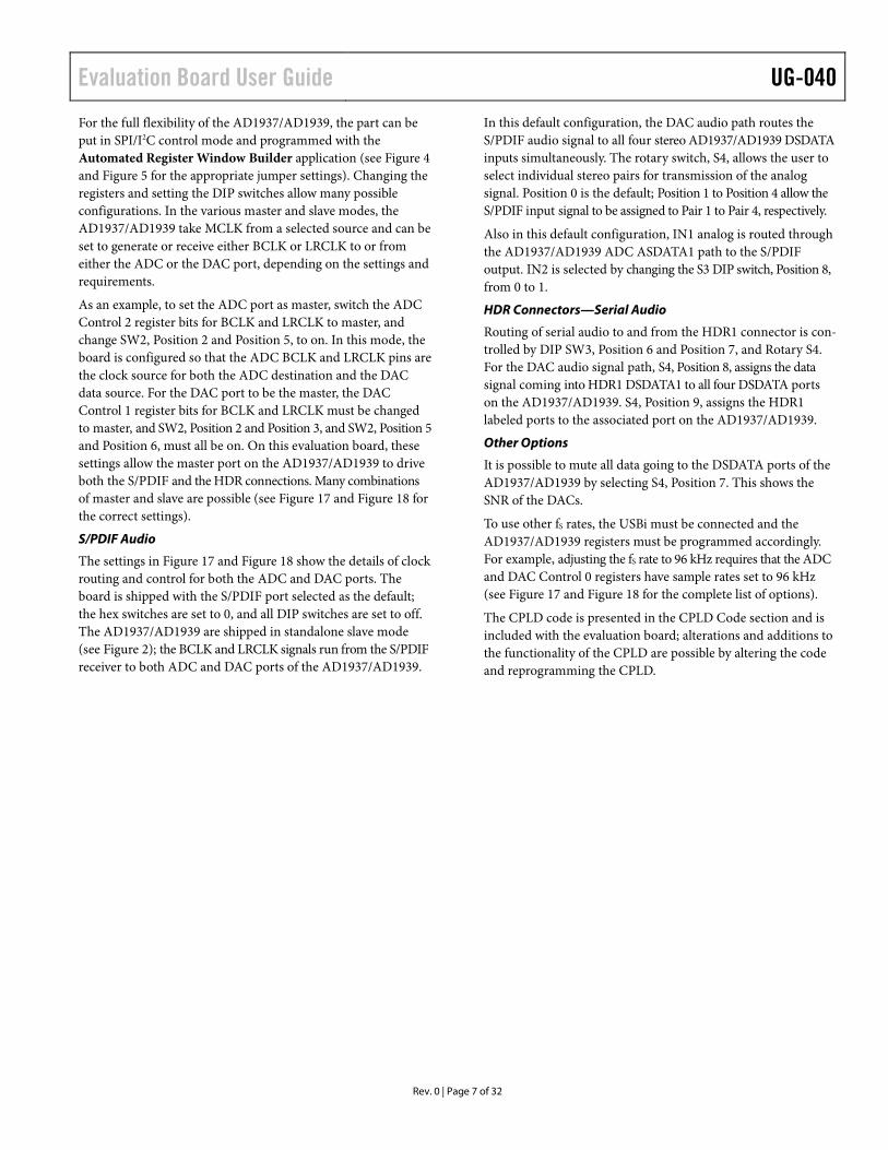
Figure 17. Settings Chart 1
Evaluation Board User Guide UG-040
Rev. 0 | Page 9 of 32
08411-018
DA
C a
ndA
DC
Se
rialD
ata
(DS
DA
TA/A
SD
ATA
) Sou
rce
Sel
ectio
nan
dR
outin
g(S
witc
hS
4an
d S
witc
hS
3)
****
*Sig
nals
ourc
es to
the
DA
C d
ata
lines
(DS
DA
TA1/
2/3/
4) fi
ll th
eco
lum
ns,c
olum
nhe
ader
is th
ede
stin
atio
n**
****
S4Po
sitio
nD
AC
Seria
lFor
mat
DA
C1
(DSD
ATA
1)D
AC
2(D
SDA
TA2)
DA
C3
(DSD
ATA
3)D
AC
4(D
SDA
TA4)
Des
crip
tion
0*S
tere
oSP
DIF
_RX
_841
6SP
DIF
_RX
_841
6SP
DIF
_RX
_841
6SP
DIF
_RX
_841
6SP
DIF
_RX
_841
6st
ereo
data
toal
leig
ht D
AC
chan
nels
1S
tere
oSP
DIF
_RX
_841
6H
DR
1_D
SD
ATA
2H
DR
1_D
SD
ATA
3H
DR
1_D
SD
ATA
4SP
DIF
_RX
_841
6st
ereo
data
to D
AC
1on
ly,r
est D
AC
s2/3
/4da
ta fr
om H
DR
1co
nnec
tor
2S
tere
oH
DR
1_D
SD
ATA
1SP
DIF
_RX
_841
6H
DR
1_D
SD
ATA
3H
DR
1_D
SD
ATA
4SP
DIF
_RX
_841
6da
ta to
DA
C2
only
,res
t DA
Cs1
/3/4
data
from
HD
R1
conn
ecto
r3
Ste
reo
HD
R1_
DS
DA
TA1
HD
R1_
DS
DA
TA2
SPD
IF_R
X_8
416
HD
R1_
DS
DA
TA4
SPD
IF_R
X_8
416
data
to D
AC
3on
ly,r
est D
AC
s1/2
/4da
ta fr
om H
DR
1co
nnec
tor
4S
tere
oH
DR
1_D
SD
ATA
1H
DR
1_D
SD
ATA
2H
DR
1_D
SD
ATA
3SP
DIF
_RX
_841
6SP
DIF
_RX
_841
6da
ta to
DA
C4
only
,res
t DA
Cs1
/2/3
data
from
HD
R1
conn
ecto
r5
N/A
N/A
N/A
N/A
N/A
6N
/AN
/AN
/AN
/AN
/A7
Ste
reo/
TDM
ZER
O D
ATA
ZER
O D
ATA
ZER
O D
ATA
ZER
O D
ATA
Sou
rce
zero
data
toal
leig
ht D
AC
chan
nels
8S
tere
oH
DR
1_D
SD
ATA
1H
DR
1_D
SD
ATA
1H
DR
1_D
SD
ATA
1H
DR
1_D
SD
ATA
1H
DR
1C
onne
ctor
Sig
nal H
DR
1_D
SD
ATA
1dr
ives
all f
our D
AC
pai
rs9
Ste
reo
HD
R1_
DS
DA
TA1
HD
R1_
DS
DA
TA2
HD
R1_
DS
DA
TA3
HD
R1_
DS
DA
TA4
HD
R1
Con
nect
orD
ata
Line
s D
SD
ATA
1, D
SD
ATA
2...
soon
driv
eco
rres
pond
ing
DA
C d
ata
lines
ATD
MH
DR
1_D
SD
ATA
1D
AC
_TD
M_O
UT
HD
R1
Con
nect
orD
ata
Line
s D
SD
ATA
1, D
SD
ATA
2...
soon
driv
e/re
ceiv
eco
rres
pond
ing
DA
C d
ata
lines
inTD
Mm
ode
BD
ual-
Line
TDM
HD
R1_
DS
DA
TA1
DA
C_T
DM
_OU
TH
DR
1_D
SD
ATA
3D
AC
_TD
M_O
UT
HD
R1
Con
nect
orD
ata
Line
s D
SD
ATA
1, D
SD
ATA
2...
soon
driv
e/re
ceiv
eco
rres
pond
ing
DA
C d
ata
lines
inTD
Mm
ode
CD
AC
aux
mod
eH
DR
1_D
SD
ATA
1A
uxA
DC
1in
put
Aux
AD
C2
inpu
tA
ux D
AC
2ou
tput
HD
R1
Con
nect
orD
ata
Line
s D
SD
ATA
1, D
SD
ATA
2...
soon
driv
e/re
ceiv
eco
rres
pond
ing
DA
C d
ata
lines
inTD
Mm
ode
D E FS
tere
o/TD
MTR
ISTA
TETR
ISTA
TETR
ISTA
TETR
ISTA
TETr
ista
teal
l DA
C d
ata
lines
, DS
DA
TA1,
DS
DA
TA2,
DS
DA
TA3,
and
DS
DA
TA4
****
* C
olum
nco
nten
tind
icat
es th
edi
rect
ion
ofth
e D
AC
dat
api
nsan
dco
rres
pond
ing
HD
R1
conn
ecto
r DA
C d
ata
pins
****
***
S4Po
sitio
nD
AC
1(D
SD
ATA
1)D
AC
2(D
SD
ATA
2)D
AC
3(D
SD
ATA
3)D
AC
4(D
SD
ATA
4)HD
R1_
DS
DA
TA1
HDR
1_D
SD
ATA
2HD
R1_
DS
DA
TA3
HDR
1_D
SD
ATA
4SP
DIF
_Rx
Dat
aHD
R1
Dat
a
0*In
put
Inpu
tIn
put
Inpu
tN
/AN
/AN
/AN
/AM
aste
r1
Inpu
tIn
put
Inpu
tIn
put
N/A
Inpu
tIn
put
Inpu
tM
aste
r2
Inpu
tIn
put
Inpu
tIn
put
Inpu
tN
/AIn
put
Inpu
tM
aste
r3
Inpu
tIn
put
Inpu
tIn
put
Inpu
tIn
put
N/A
Inpu
tM
aste
r4
Inpu
tIn
put
Inpu
tIn
put
Inpu
tIn
put
Inpu
tN
/AM
aste
r5 6 7
Inpu
tIn
put
Inpu
tIn
put
Out
put
Out
put
Out
put
Out
put
N/A
N/A
8In
put
Inpu
tIn
put
Inpu
tIn
put
Inpu
tIn
put
Inpu
tM
aste
r9
Inpu
tIn
put
Inpu
tIn
put
Inpu
tIn
put
Inpu
tIn
put
Mas
ter
AIn
put
Out
put
Inpu
tO
utpu
tM
aste
rB
Inpu
tO
utpu
tIn
put
Out
put
Inpu
tO
utpu
tIn
put
Out
put
Mas
ter
CIn
put
Inpu
tIn
put
Out
put
Inpu
tIn
put
Inpu
tO
utpu
tM
aste
rD E F
TRIS
TATE
TRIS
TATE
TRIS
TATE
TRIS
TATE
DIP
Switc
hS3
Posi
tion:
Posi
tion-
6Po
sitio
n-7
AD
CSe
rialF
orm
atH
DR
1_A
SDA
TA1
HD
R1_
ASD
ATA
2D
escr
iptio
n(H
DR
1A
DC
Dat
aSo
urce
Sele
ctio
n)O
ff*O
ff*S
tere
oAS
DA
TA1
ASD
ATA
2H
DR
1C
onne
ctor
AD
C D
ata
Line
sA
SD
ATA
1an
dAS
DA
TA2
rece
ive
corr
espo
ndin
gA
DC
dat
ast
ream
Off
On
Ste
reo
ASD
ATA
2AS
DA
TA2
HD
R1
Con
nect
orA
DC
Dat
aLi
neA
SD
ATA
1re
ceiv
eA
DC
2da
talin
eA
SD
ATA
2O
nO
ffTD
MAS
DA
TA1
AD
CTD
Min
puts
tream
HD
R1
Con
nect
orA
DC
Dat
aLi
neA
SD
ATA
1re
ceiv
eA
DC
TDM
outd
ata
stre
amO
nO
nA
DC
Aux
(see
note
)AS
DA
TA1
AD
CTD
Min
puts
tream
HD
R1
Con
nect
orA
DC
Dat
aLi
neA
SD
ATA
1re
ceiv
eA
DC
TDM
outd
ata
stre
am
NO
TE: A
DC
AU
Xm
ode
over
ride
sth
eD
AC
data
conf
igur
atio
nro
tary
Switc
hS2
sett
ing.
DIP
Switc
hS3
Posi
tion:
Posi
tion-
6Po
sitio
n-7
HD
R1_
ASD
ATA
1H
DR
1_A
SDA
TA2
AD
C1
(ASD
ATA
1)A
DC
2(A
SDA
TA2)
Off*
Off*
Out
put
Out
put
Out
put
Out
put
Off
On
Out
put
Out
put
Out
put
Out
put
On
Off
Out
put
Inpu
tO
utpu
tIn
put
On
On
Out
put
Inpu
tO
utpu
tIn
put
DIP
Switc
hS3
Posi
tion:
Posi
tion-
8O
ff*A
DC
1D
ata
Stre
amA
SD
ATA
1is
sour
ced
to th
eSP
DIF
_Tx_
8406
.O
nA
DC
2D
ata
Stre
amA
SD
ATA
2is
sour
ced
to th
eSP
DIF
_Tx_
8406
.
Rot
ary
hex
Sw
itch
S4
sele
cts
the
AD
193x
DA
Cse
riald
ata
sour
ce. T
he D
AC
dat
aso
urce
can
beei
ther
SP
DIF
Rec
eive
r CS
8416
orca
nbe
prov
ided
by th
eH
eade
rCon
nect
or H
DR
1.It
isim
porta
nt to
note
that
the
DA
C d
ata
sour
cesh
ould
bein
sync
with
the
DA
Cse
rialp
ortc
lock
sour
ce(s
etby
DIP
Sw
itch
S2,
Pos
ition
s [5
:6]).
DIP
Sw
itch
S3
rout
es th
eAD
Cse
riald
ata
amon
gA
D19
3x,S
PD
IF T
rans
mitt
er C
S84
06,a
ndH
eade
rCon
nect
or H
DR
1in
ster
eo,T
DM
,and
aux
mod
e.
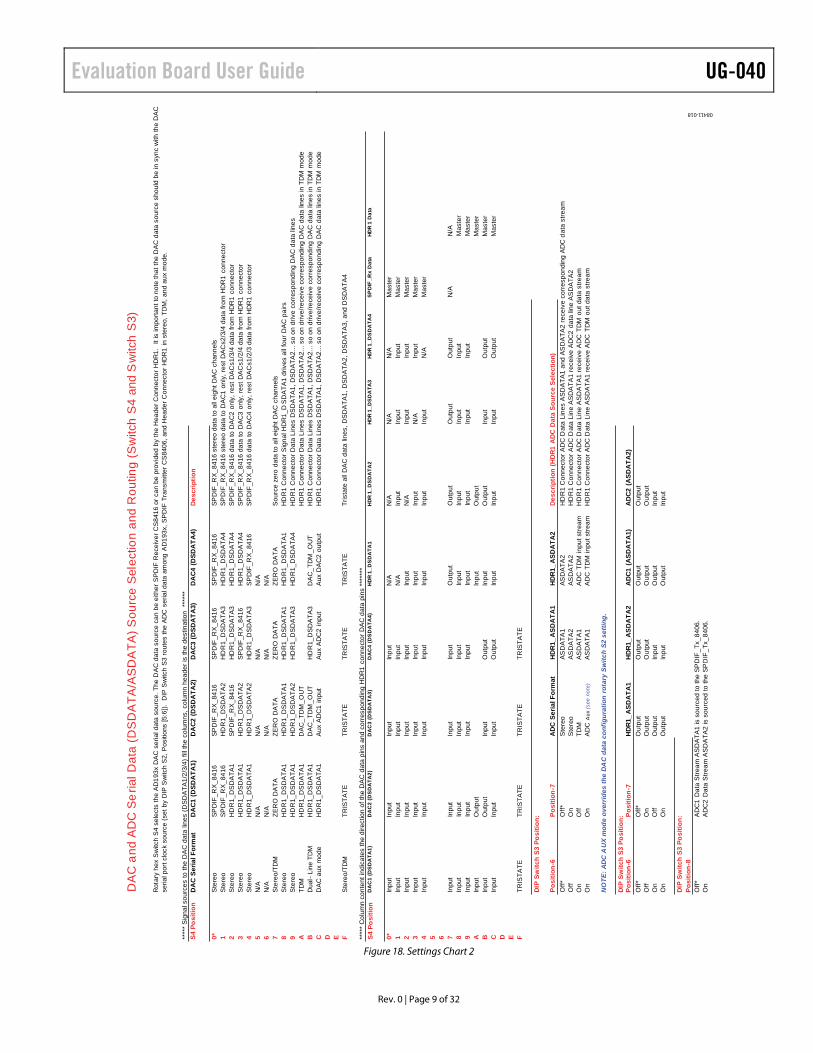
Figure 18. Settings Chart 2

UG-040 Evaluation Board User Guide
Rev. 0 | Page 10 of 32
SCHEMATICS AND ARTWORK
08411-019
Figure 19. Board Schematics, Page 1—ADC Buffer Circuits

Evaluation Board User Guide UG-040
Rev. 0 | Page 11 of 32
08411-020
Figure 20. Board Schematics, Page 2—Serial Digital Audio Interface Headers with MCLK Direction Switching

UG-040 Evaluation Board User Guide
Rev. 0 | Page 12 of 32
08411-021
Figure 21. Board Schematics, Page 3—S/PDIF Receive and Transmit Interfaces

Evaluation Board User Guide UG-040
Rev. 0 | Page 13 of 32
08411-022
Figure 22. Board Schematics, Page 4—Serial Digital Audio Routing and Control CPLD

UG-040 Evaluation Board User Guide
Rev. 0 | Page 14 of 32
08411-023
Figure 23. Board Schematics, Page 5—AD1937/AD1939 with MCLK Selection Jumpers

Evaluation Board User Guide UG-040
Rev. 0 | Page 15 of 32
0841
1-02
4
Figure 24. Board Schematics, Page 6—Daughter Card Interface, Useful as Test Points

UG-040 Evaluation Board User Guide
Rev. 0 | Page 16 of 32
08411-025
Figure 25. Board Schematics, Page 7—DAC Buffer Circuits

Evaluation Board User Guide UG-040
Rev. 0 | Page 17 of 32
0841
1-02
6
Figure 26. Board Schematics, Page 8—SPI and I2C Control Interface

UG-040 Evaluation Board User Guide
Rev. 0 | Page 18 of 32
0841
1-02
7
Figure 27. Board Schematics, Page 9—Power Supply

Evaluation Board User Guide UG-040
Rev. 0 | Page 19 of 32
0841
1-02
8
Figure 28. Top Assembly Layer

UG-040 Evaluation Board User Guide
Rev. 0 | Page 20 of 32
0841
1-02
9
Figure 29. Bottom Assembly Layer

Evaluation Board User Guide UG-040
Rev. 0 | Page 21 of 32
CPLD CODE MODULE IF_Logic
TITLE 'AD1939 EVB Input Interface Logic'
//===================================================================================
// FILE: AD1939_pld_revE.abl
// REVISION DATE: 04-16-09 (rev-E)
// REVISION: E
// DESCRIPTION:
//===================================================================================
LIBRARY 'MACH';
"INPUTS ----------------------------------------------------------------------------
// AD1939 CODEC pins
DSDATA1,DSDATA2 pin 86, 87 istype 'com';
DSDATA3,DSDATA4 pin 91, 92 istype 'com';
DBCLK,DLRCLK pin 85, 84 istype 'com';
ASDATA1,ASDATA2 pin 80, 81 istype 'com';
ABCLK,ALRCLK pin 78, 79 istype 'com';
// 25-pin header connector HDR1 pins
HDR1_DSDATA1 pin 20 istype 'com';
HDR1_DSDATA2 pin 19 istype 'com';
HDR1_DSDATA3 pin 17 istype 'com';
HDR1_DSDATA4 pin 16 istype 'com';
HDR1_DBCLK pin 21 istype 'com';
HDR1_DLRCLK pin 22 istype 'com';
HDR1_ASDATA1 pin 29 istype 'com, buffer';
HDR1_ASDATA2 pin 28 istype 'com, buffer';
HDR1_ABCLK pin 30 istype 'com';
HDR1_ALRCLK pin 31 istype 'com';
// 25-pin header connector HDR2 pins
HDR2_DSDATA1 pin 37 istype 'com';
HDR2_DSDATA2 pin 36 istype 'com';
HDR2_DSDATA3 pin 35 istype 'com';
HDR2_DSDATA4 pin 34 istype 'com';
HDR2_DBCLK pin 41 istype 'com';
HDR2_DLRCLK pin 42 istype 'com';
HDR2_ASDATA1 pin 44 istype 'com';
HDR2_ASDATA2 pin 43 istype 'com, buffer';
HDR2_ABCLK pin 47 istype 'com';
HDR2_ALRCLK pin 48 istype 'com';
// S/PDIF Rx CS8414 pins
SDATA_8416 pin 61 istype 'com';

UG-040 Evaluation Board User Guide
Rev. 0 | Page 22 of 32
BCLK_8416 pin 60 istype 'com';
LRCLK_8416 pin 59 istype 'com';
SOMS_RX,SFSEL1_RX,SFSEL0_RX,RMCKF_RX pin 66,67,64,65 istype 'com';
// S/PDIF Tx CS8404 pins
SDATA_8406 pin 50 istype 'com';
BCLK_8406,LRCLK_8406 pin 53, 54 istype 'com';
MCLK_8406 pin 49 istype 'com';
APMS_TX,SFMT1_TX,SFMT0_TX pin 55,56,58 istype 'com';
CPLD_MCLK pin 89 istype 'com';
// AD1939 SPI port pins
//CCLK,CDATA,CLATCH pin 84, 83, 85 istype 'com';
//COUT pin 82 istype 'com';
//CLATCH2,CLATCH3,CLATCH4 pin 86, 56, 4 istype 'com';
//CONTROL_ENB pin 81 istype 'com';
S/PDIF_RESET_OUT pin 69 istype 'com';
// Switch S1, S2, S3 and S4 pins
ADC_CLK_OFF pin 93 istype 'com'; // S2-1
ADC_CLK_SRC1 pin 94 istype 'com'; // S2-2
ADC_CLK_SRC0 pin 97 istype 'com'; // S2-3
DAC_CLK_OFF pin 98 istype 'com'; // S2-4
DAC_CLK_SRC1 pin 99 istype 'com'; // S2-5
DAC_CLK_SRC0 pin 100 istype 'com'; // S2-6
S/PDIF_MCLK_RATE pin 3 istype 'com'; // S2-7
S/PDIF_RESET_IN pin 4 istype 'com'; // S2-8
MODE11,MODE12,MODE13,MODE14 pin 5,6,8,9 istype 'com'; // S4
STAND_ALONE,MODE22,MODE23,MODE24 pin 10,11,14,15 istype 'com'; // S5
"NODES
I_DSDATA1, I_DSDATA2, I_DSDATA3, I_DSDATA4 node istype 'com';
I_DBCLK, I_DLRCLK node istype 'com';
I_ASDATA1, I_ASDATA2 node istype 'com, buffer';
I_ABCLK, I_ALRCLK node istype 'com';
Qdivide node istype 'reg, buffer';

Evaluation Board User Guide UG-040
Rev. 0 | Page 23 of 32
//================================================================================
"MACROS
// Switch S3, DIP POSITIONS 6 AND 7
ADC_HDR_NORMAL = ( MODE22 & MODE23);
ADC_HDR_DATA2_DATA1 = ( MODE22 & !MODE23);
ADC_HDR_TDM = (!MODE22 & MODE23);
ADC_HDR_AUX = (!MODE22 & !MODE23);
S/PDIF_OUT_MUX = MODE24;
// Hex Switch S4
// S4 position 0,
DAC_RX_ALL = ( MODE14 & MODE13 & MODE12 & MODE11);
// S4 position 1,
DAC_RX_1 = ( MODE14 & MODE13 & MODE12 & !MODE11);
// S4 position 2,
DAC_RX_2 = ( MODE14 & MODE13 & !MODE12 & MODE11);
// S4 position 3,
DAC_RX_3 = ( MODE14 & MODE13 & !MODE12 & !MODE11);
// S4 position 4,
DAC_RX_4 = ( MODE14 & !MODE13 & MODE12 & MODE11);
// S4 position 5,
NA1 = ( MODE14 & !MODE13 & MODE12 & !MODE11);
// S4 position 6,
NA2 = ( MODE14 & !MODE13 & !MODE12 & MODE11);
// S4 position 7,
DAC_DATA_ZERO = ( MODE14 & !MODE13 & !MODE12 & !MODE11);
// S4 position 8,
DAC_HDR1_ALL = ( !MODE14 & MODE13 & MODE12 & MODE11);
// S4 position 9,
DAC_HDR1_IND = ( !MODE14 & MODE13 & MODE12 & !MODE11);
// S4 position A,
DAC_HDR1_TDM = ( !MODE14 & MODE13 & !MODE12 & MODE11);

UG-040 Evaluation Board User Guide
Rev. 0 | Page 24 of 32
// S4 position B,
DAC_DUAL_TDM = ( !MODE14 & MODE13 & !MODE12 & !MODE11);
// S4 position C,
DAC_HDR1_AUX = ( !MODE14 & !MODE13 & MODE12 & MODE11);
// S4 position D,
NA3 = ( !MODE14 & !MODE13 & MODE12 & !MODE11);
// S4 position E,
NA4 = ( !MODE14 & !MODE13 & !MODE12 & MODE11);
// S4 position F,
DAC_DATA_HIZ = ( !MODE14 & !MODE13 & !MODE12 & !MODE11);
// Switch S2
DAC_S/PDIF = (DAC_CLK_SRC1 & DAC_CLK_SRC0);
DAC_HDR1 = (DAC_CLK_SRC1 & !DAC_CLK_SRC0);
DAC_ADC = (!DAC_CLK_SRC1 & DAC_CLK_SRC0);
DAC_DAC = (!DAC_CLK_SRC1 & !DAC_CLK_SRC0);
ADC_S/PDIF = (ADC_CLK_SRC1 & ADC_CLK_SRC0);
ADC_HDR1 = (ADC_CLK_SRC1 & !ADC_CLK_SRC0);
ADC_ADC = (!ADC_CLK_SRC1 & ADC_CLK_SRC0);
ADC_DAC = (!ADC_CLK_SRC1 & !ADC_CLK_SRC0);
"====================================================================================
EQUATIONS
S/PDIF_RESET_OUT = S/PDIF_RESET_IN;
// Configuration of the CS8416, changes active on reset, BCLK_8416 and LRCLK_8416 are bi-directional signals.
SOMS_RX = DAC_S/PDIF; // SOMS = Serial Output Master/Slave Select
SFSEL1_RX = 0; //DIR_RJ # DIR_RJ16; // SFSEL1 = Serial Format Select 1
SFSEL0_RX = 1; //DIR_I2S # DIR_DSP; // SFSEL0 = Serial Format Select 0
RMCKF_RX = !S/PDIF_MCLK_RATE; // RMCKF = Receive Master Clock Frequency
// M0_8414 = (0 # !DAC_S/PDIF);
// M1_8414 = 1;
// M2_8414 = 0;
Evaluation Board User Guide UG-040
Rev. 0 | Page 25 of 32
// M3_8414 = 0;
// CS8404 Tx interface mode select
APMS_TX = 0; // Tx serial port is always slave in this application
SFMT1_TX = 0; // Tx data format is I2S always
SFMT0_TX = 1;
// M0_8404 = 0;
// M1_8404 = 0;
// M2_8404 = 1; // I2S format only
// divide 256Fs clock by 2 for 128Fs clock to the S/PDIF Tx
// Qdivide.clk = CPLD_MCLK;
// Qdivide.d = !Qdivide;
// MCLK_8406 = Qdivide;
MCLK_8406 = CPLD_MCLK;
BCLK_8406 = I_ABCLK;
LRCLK_8406 = I_ALRCLK;
SDATA_8406 = (ASDATA1 & S/PDIF_OUT_MUX) # (ASDATA2 & !S/PDIF_OUT_MUX);
// For SPI mode, let external port drive the SPI port
DBCLK.oe = (DAC_S/PDIF # DAC_HDR1 # DAC_ADC # !DAC_DAC) & (DAC_CLK_OFF);
DLRCLK.oe = (DAC_S/PDIF # DAC_HDR1 # DAC_ADC # !DAC_DAC) & (DAC_CLK_OFF);
ABCLK.oe = (ADC_S/PDIF # ADC_HDR1 # !ADC_ADC # ADC_DAC) & (ADC_CLK_OFF);
ALRCLK.oe = (ADC_S/PDIF # ADC_HDR1 # !ADC_ADC # ADC_DAC) & (ADC_CLK_OFF);
HDR1_DBCLK.oe = (DAC_S/PDIF # !DAC_HDR1 # DAC_ADC # DAC_DAC);
HDR1_DLRCLK.oe = (DAC_S/PDIF # !DAC_HDR1 # DAC_ADC # DAC_DAC);
HDR1_ABCLK.oe = (ADC_S/PDIF # !ADC_HDR1 # ADC_ADC # ADC_DAC);
HDR1_ALRCLK.oe = (ADC_S/PDIF # !ADC_HDR1 # ADC_ADC # ADC_DAC);
BCLK_8416.oe = (!DAC_S/PDIF);
LRCLK_8416.oe = (!DAC_S/PDIF);
BCLK_8416 = I_DBCLK;
LRCLK_8416 = I_DLRCLK;
DSDATA1.oe = (!DAC_DATA_HIZ);
DSDATA2.oe = (!(DAC_HDR1_TDM # DAC_DUAL_TDM # DAC_DATA_HIZ)); //DSDATA2 is output in DAC TDM-daisy chain mode
DSDATA3.oe = (!DAC_DATA_HIZ);
DSDATA4.oe = (!(DAC_DUAL_TDM # ADC_HDR_AUX # DAC_HDR1_AUX # DAC_DATA_HIZ)); // SECOND TDM-OUT IN DUAL LINE DAC TDM MODE
ASDATA2.oe = (ADC_HDR_TDM); //ASDATA2 is input in ADC TDM mode
HDR1_DSDATA2.oe = (DAC_HDR1_TDM # DAC_DUAL_TDM);

UG-040 Evaluation Board User Guide
Rev. 0 | Page 26 of 32
HDR1_DSDATA4.oe = (DAC_DUAL_TDM # ADC_HDR_AUX # DAC_HDR1_AUX);
HDR1_ASDATA2.oe = (!ADC_HDR_TDM);
DBCLK = I_DBCLK;
DLRCLK = I_DLRCLK;
ABCLK = I_ABCLK;
ALRCLK = I_ALRCLK;
DSDATA1 = (HDR1_DSDATA1 & (DAC_HDR1_ALL # DAC_HDR1_IND # DAC_RX_2 # DAC_RX_3 # DAC_RX_4 # DAC_HDR1_TDM # DAC_DUAL_TDM # ADC_HDR_AUX))
# (SDATA_8416 & (DAC_RX_ALL # DAC_RX_1)) # (0 & DAC_DATA_ZERO);
DSDATA2 = (HDR1_DSDATA1 & DAC_HDR1_ALL) # (HDR1_DSDATA2 & (DAC_HDR1_IND # ADC_HDR_AUX # DAC_HDR1_AUX # DAC_RX_1 # DAC_RX_3 # DAC_RX_4))
# (SDATA_8416 & (DAC_RX_ALL # DAC_RX_2)) # (0 & DAC_DATA_ZERO);
DSDATA3 = (HDR1_DSDATA1 & (DAC_HDR1_ALL)) # (HDR1_DSDATA3 & (DAC_HDR1_IND # DAC_DUAL_TDM # ADC_HDR_AUX # DAC_HDR1_AUX # DAC_RX_1 # DAC_RX_2 # DAC_RX_4))
# (SDATA_8416 & (DAC_RX_ALL # DAC_RX_3)) # (0 & DAC_DATA_ZERO);
DSDATA4 = (HDR1_DSDATA1 & (DAC_HDR1_ALL)) # (HDR1_DSDATA4 & (DAC_HDR1_IND # DAC_RX_1 # DAC_RX_2 # DAC_RX_3))
# (SDATA_8416 & (DAC_RX_ALL # DAC_RX_4)) # (0 & DAC_DATA_ZERO);
HDR1_DBCLK = I_DBCLK;
HDR1_DLRCLK = I_DLRCLK;
HDR1_ABCLK = I_ABCLK;
HDR1_ALRCLK = I_ALRCLK;
HDR1_ASDATA1 = (ASDATA1 & (ADC_HDR_NORMAL # ADC_HDR_TDM # ADC_HDR_AUX # DAC_HDR1_AUX )) # (ASDATA2 & ADC_HDR_DATA2_DATA1);
HDR1_ASDATA2 = ASDATA2;
ASDATA2 = HDR1_ASDATA2;
HDR1_DSDATA2 = DSDATA2;
HDR1_DSDATA4 = DSDATA4;
// Internal node signals
I_DBCLK = (BCLK_8416 & DAC_S/PDIF) # (HDR1_DBCLK & DAC_HDR1) # (DBCLK & DAC_DAC) # (I_ABCLK & DAC_ADC);
I_DLRCLK = (LRCLK_8416 & DAC_S/PDIF) # (HDR1_DLRCLK & DAC_HDR1) # (DLRCLK & DAC_DAC) # (I_ALRCLK & DAC_ADC);
I_ABCLK = (BCLK_8416 & ADC_S/PDIF) # (HDR1_ABCLK & ADC_HDR1) # (ABCLK & ADC_ADC) # (I_DBCLK & ADC_DAC);
I_ALRCLK = (LRCLK_8416 & ADC_S/PDIF) # (HDR1_ALRCLK & ADC_HDR1) # (ALRCLK & ADC_ADC) # (I_DLRCLK & ADC_DAC);
"====================================================================================
END IF_Logic

Evaluation Board User Guide UG-040
Rev. 0 | Page 27 of 32
ORDERING INFORMATION BILL OF MATERIALS
Table 1. Qty Designator Description Manufacturer Part Number 18 C85, C90 to C94, C101 to C103,
C107, C108, C110, C115, C116, C121, C127, C132, C134
Multilayer ceramic capacitor,16 V, X7R (0402)
Panasonic EC ECJ-0EX1C104K
50 C1, C2, C5, C7 to C10, C20, C21, C28, C29, C38, C42, C48 to C51, C58 to C60, C62, C64, C69, C73, C76, C79, C82, C97, C99, C112, C118, C122, C128, C135, C146, C147, C149, C151, C155, C156, C158, C162, C168, C174, C176, C177, C193, C194, C197, C203
Multilayer ceramic capacitor, 50 V, X7R (0603)
Panasonic EC ECJ-1VB1H104K
9 C37, C65, C67, C83, C88, C124, C129, C157, C160
Multilayer ceramic capacitor, 50 V, NP0 (0603)
Panasonic EC ECJ-1VC1H102J
12 R28, R30, R51, R59, R166, R167, R169, R172, R185, R189, R212, R214
Chip resistor, 100 kΩ, 1%, 125 mW, thick film (0603)
Panasonic EC ERJ-3EKF1003V
8 C68, C71, C87, C89, C130, C138, C159, C161
Multilayer ceramic capacitor, 50 V, NP0 (0603)
Panasonic EC ECJ-1VC1H101J
16 R24, R31, R44, R60, R77, R84, R93, R106, R136, R149, R159, R170, R180, R191, R207, R217
Chip resistor, 100 kΩ, 1%, 100 mW, thick film (0603)
Panasonic EC ERJ-3EKF1000V
1 C84 Aluminum electrolytic capacitor, 100 μF, 16 V, FC 105 deg, SMD_E
Panasonic EC EEE-FC1C101P
32 R6, R7, R13, R14, R18, R20, R40, R43, R47 to R49, R54, R55, R63, R64, R74, R78, R80, R82, R158, R164, R186, R224 to R227, R232 to R237
Chip resistor, 10 kΩ, 1%, 125 mW, thick film (0603)
Panasonic EC ERJ-3EKF1002V
3 C6, C39, C40 Multilayer ceramic capacitor, 25 V, NP0 (0603)
TDK Corp C1608C0G1E103J
12 C15 to C17, C81, C86, C95, C98, C170, C175, C178, C180, C183
Multilayer ceramic capacitor, 100 V, NP0 (0603)
Panasonic EC ECJ-1VC2A100D
12 C104, C106, C109, C111, C117, C123, C140 to C145
Multilayer ceramic capacitor, 50 V, NP0 (0402)
Kemet C0402C100J5GACTU
5 C3, C4, C74, C96, C126 Aluminum electrolytic capacitor, 16 V, FC 105 deg, SMD_B
Panasonic EC EEE-FC1C100R
4 C61, C77, C113, C150 Multilayer ceramic capacitor, 50 V NP0 (0603)
Panasonic EC ECJ-1VC1H121J
1 R117 Chip resistor, 1 kΩ, 1% 125 mW thick film (0603)
Panasonic EC ERJ-3EKF1001V
3 D1, D3, D4 TVS Zener, 15 V, 600 W, SMB ON Semiconductor 1SMB15AT3G 9 C23, C33, C43, C55, C114, C166,
C184, C188, C200 Multilayer ceramic capacitor, 50 V, NP0 (0603)
Murata Electronics GRM1885C1H222JA01D
1 C36 Multilayer ceramic capacitor, 50 V, NP0 (0805)
Murata ENA GRM21B5C1H223JA01L
2 C153, C154 Multilayer ceramic capacitor, 50 V, NP0 (0603)
Panasonic EC ECJ-1VC1H220J
8 R76, R81, R90, R101, R134, R141, R157, R168
Chip resistor, 237 Ω, 1%, 125 mW, thick film (0603)
Panasonic EC ERJ-3EKF2370V
2 R1, R4 Chip resistor, 243 Ω, 1%, 100 mW, thick film (0603)
Panasonic EC ERJ-3EKF2430V
10 R91, R94, R98, R99, R108, R109, R114, R115, R118, R123
Chip resistor, 24.9 Ω, 1%, 63 mW, thick film (0402)
Rohm MCR01MZPF24R9

UG-040 Evaluation Board User Guide
Rev. 0 | Page 28 of 32
Qty Designator Description Manufacturer Part Number 16 R56, R57, R65, R66, R88, R89, R140,
R154, R179, R183, R213, R216, R228 to R231
Chip resistor, 24.9 Ω, 1%, 100 mW, thick film (0603)
Rohm MCR03EZPFX24R9
16 C24, C25, C31, C34, C44, C45, C53, C56, C167, C169, C181, C185, C189, C190, C198, C201
Multilayer ceramic capacitor, 100 V, NP0 (0603)
Murata ENA GRM1885C2A301JA01D
3 R3, R11, R58 Chip resistor, 374 Ω, 1%, 100 mW, thick film (0603)
Rohm MCR03EZPFX3740
1 C125 Multilayer ceramic capacitor, 50 V, NP0 (0603)
Panasonic EC ECJ-1VC1H391J
4 R5, R52, R53, R75 Chip resistor, 392 Ω, 1%, 100 mW, thick film (0603)
Rohm MCR03EZPFX3920
1 C120 Multilayer ceramic capacitor, 16 V, ECH-U (1206)
Panasonic EC ECH-U1C393JB5
33 R21, R22, R26, R27, R33 to R35, R37 to R39, R41, R46, R50, R62, R68, R69, R71, R173, R176, R182, R184, R193, R195, R197, R199, R202, R204, R209, R211, R219 to R221, R223
Chip resistor, 3.01 kΩ, 1%, 100 mW, thick film (0603)
Rohm MCR03EZPFX3011
16 R23, R25, R32, R36, R42, R45, R61, R70, R177, R181, R192, R198, R205, R208, R218, R222
Chip resistor, 3.09 kΩ, 1%, 100 mW, thick film (0603)
Rohm MCR03EZPFX3091
1 R129 Chip resistor, 3.32 kΩ, 1%, 100 mW, thick film (0603)
Rohm MCR03EZPFX3321
23 C11, C13, C14, C26, C30, C46, C52, C63, C66, C72, C75, C80, C105, C119, C133, C139, C148, C152, C164, C172, C179, C191, C196
Aluminum electrolytic capacitor, 16 V, FC 105 deg, SMD_D
Panasonic EC EEE-FC1C470P
3 C12, C18, C19 Aluminum electrolytic capacitor FC 105 deg SMD_E
Panasonic EC EEE-FC1E470P
1 R12 Chip resistor, 499 Ω, 1%, 100 mW, thick film (0603)
Rohm MCR03EZPFX4990
4 R83, R96, R148, R163 Chip resistor, 49.9 Ω, 1%, 100 mW, thick film (0603)
Panasonic EC ERJ-3EKF4992V
20 R103, R104, R110 to R112, R116, R119, R124, R126 to R128, R130 to R132, R142 to R147
Chip resistor, 49.9 Ω, 1%, 63 mW, thick film (0402)
Rohm MCR01MZPF49R9
35 R8 to R10, R15 to R17, R19, R92, R95, R100, R105, R113, R120, R125, R133, R135, R139, R153, R155, R156, R160, R174, R175, R178, R187, R188, R190, R194, R196, R200, R201, R203, R206, R210, R215
Chip resistor, 49.9 Ω, 1%, 100 mW, thick film (0603)
Panasonic EC ERJ-3EKF49R9V
1 C131 Multilayer ceramic capacitor, 25 V, NP0 (0603)
TDK Corp C1608C0G1E562J
1 R138 Chip resistor, 562 Ω, 1%, 125 mW, thick film (0603)
Panasonic EC ERJ-3EKF5620V
16 R72, R73, R79, R85 to R87, R97, R107, R121, R122, R137, R150 to R152, R165, R171
Chip resistor, 5.76 kΩ, 1%, 125 mW, thick film (0603)
Panasonic EC ERJ-3EKF5761V
4 C78, C137, C171, C195 Multilayer ceramic capacitor, 100 V, NP0 (0603)
Panasonic EC ECJ-1VC2A680J
1 R2 Chip resistor, 715 Ω, 1%, 100 mW, thick film (0603)
Rohm MCR03EZPFX7150
1 U11 IC inverter hex, TTL/LSTTL, 14 SOIC NXP Semi 74HC04D-T 2 U19, U26 IC buffer, quad three-state, 14 SOIC Texas Instruments SN74LV125AD 1 R29 Chip resistor, 75 Ω, 1%, 100 mW, thick film Panasonic EC ERJ-3EKF75R0V

Evaluation Board User Guide UG-040
Rev. 0 | Page 29 of 32
Qty Designator Description Manufacturer Part Number (0603)
1 R67 Chip resistor, 90.9 Ω, 1%, 100 mW, thick film (0603)
Rohm MCR03EZPFX90R9
16 C22, C27, C32, C35, C41, C47, C54, C57, C165, C173, C182, C186, C187, C192, C199, C202
Multilayer ceramic capacitor, 50 V, NP0 (0603)
Murata ENA GRM1885C1H911JA01D
1 Y1 Crystal, 12.288 MHz, SMT, 10 pF Abracon Corp ABM3B-12.288MHZ-10-1-U-T
1 U15 Four ADC/eight DAC with PLL, 192 kHz Analog Devices AD1939YSTZ 1 U23 Microprocessor voltage supervisor Analog Devices ADM811RARTZ 1 U1 Voltage regulator, low dropout Analog Devices ADP3303ARZ-3.3 1 J2 5-way binding post, black, uninsulated base
TH Deltron Components
552-0100 BLK
1 J3 5-way binding post, mini, green, uninsulated base TH
Deltron Components
552-0400 GRN
1 J4 5-way binding post, mini, red, uninsulated base TH
Deltron Components
552-0500 RED
2 J22, J23 SMA receptacle straight PCB mount Amp-RF Division 901-144-8RFX 1 U8 192 kHz digital audio receiver, 28-TSSOP Cirrus Logic CS8416-CZZ 1 U13 192 kHz digital audio, S/PDIF transmitter Cirrus Logic CS8406-CZZ 2 D2, D5 Passivated rectifier, 1 A 50 V MELF Micro Commercial DL4001-TP 1 S1 Switch slide, DP3T, PC MNT, L = 4 mm E-Switch EG2305 1 SW1 DPDT slide switch, vertical E-Switch EG2207 6 L2 to L7 Chip ferrite bead, 600 Ω at 100 MHz TDK MPZ1608S601A 1 L1 Chip ferrite bead, 600 Ω at 100 MHz Steward HZ0805E601R-10 2 J1, J14 10-way shrouded polarized header 3M N2510-6002RB 4 J15 to J18 16-way unshrouded, not populated 3M N/A 1 J19 Connector header, 0.100 dual STR, 72 POS Sullins PBC10DAAN; or cut
PBC36DAAN 2 J20, J26 Connector header, 0.100 dual STR, 72 POS Sullins PBC13DAAN; or cut
PBC36DAAN 4 J5 to J8 Connector header, 0.100 dual STR, 72 POS Sullins PBC06DAAN; or cut
PBC36DAAN 2 S4, S5 16-position rotary switch hex APEM PT65503 16 JP4, JP11 to JP14, JP17, JP18, JP20
to JP22, JP24, JP26, JP28 to JP31 2-pin header, unshrouded jumper, 0.10"; use shunt Tyco 881545-2
Sullins PBC02SAAN; or cut PBC36SAAN
15 JP1 to JP3, JP5 to JP10, JP15, JP16, JP19, JP23, JP25, JP27
3-position SIP header Sullins PBC03SAAN; or cut PBC36SAAN
1 U16 Complex programmable logic device (CPLD), HI PERF E2CMOS PLD
Lattice Semiconductor
LC4128V-75TN100C
2 D8, D11 Green, diffused, 10 millicandela, 565 nm (1206)
Lumex Opto SML-LX1206GW-TR
2 D6, D9 Red, diffused, 6.0 millicandela, 635 nm (1206)
Lumex Opto SML-LX1206IW-TR
2 D7, D10 Yellow, diffused, 4.0 millicandela, 585 nm (1206)
CML Innovative Tech
CMD15-21VYD/TR8
2 U2, U3 3-terminal adjustable voltage regulator, DPak
STMicroelectronics LM317MDT-TR
6 J10, J11, J13, J21, J27, J28 Stereo mini jack SMT CUI SJ-3523-SMT 2 R161, R162 Resistor network, bussed 8 res, 9 pin CTS 773091103 8 U6, U9, U12, U14, U17, U20, U24,
U25 Dual bipolar/JFET audio op amp Analog Devices OP275GSZ
1 R102 Not populated N/A N/A 1 U21 12.288 MHz fixed SMD oscillator, 1.8 V dc to
3.3 V dc Abracon Corp AP3S-12.288MHz-F-J-B
2 J9, J12 RCA jack PCB TH mount R/A yellow Connect-Tech Products
CTP-021A-S-YEL

UG-040 Evaluation Board User Guide
Rev. 0 | Page 30 of 32
Qty Designator Description Manufacturer Part Number 1 U10 110 Ω AES/EBU transformer Scientific
Conversion SC937-02
2 U18, U22 Buffer, three-state single gate Texas Instruments SN74LVC1G125DRLR 1 U4 Octal, three-state buffer/driver Texas Instruments SN74LVC541ADBR 2 SW2, SW3 SPDT slide switch, PC mount E-Switch EG1218 2 S2, S3 8-position, SPST SMD switch, flush,
actuated CTS 219-8LPST
1 S6 Tact switch, 6 mm, gull wing Tyco/Alcoswitch FSM6JSMA 1 U5 15 Mb/sec fiber optic receiving module
with shutter Toshiba TORX147L(F,T)
1 U7 15 Mb/sec fiber optic transmit module, Toshiba TOTX147L(F,T) 69 TP1 to TP69 Mini test point, white, 0.1 inch, OD Keystone
Electronics 5002
1 Q1 100 V, medium power, low saturation transistor, SOT223, NPN
Zetex ZX5T953GTA

Evaluation Board User Guide UG-040
Rev. 0 | Page 31 of 32
NOTES

UG-040 Evaluation Board User Guide
Rev. 0 | Page 32 of 32
NOTES
I2C refers to a communications protocol originally developed by Philips Semiconductors (now NXP Semiconductors).
ESD Caution ESD (electrostatic discharge) sensitive device. Charged devices and circuit boards can discharge without detection. Although this product features patented or proprietary protection circuitry, damage may occur on devices subjected to high energy ESD. Therefore, proper ESD precautions should be taken to avoid performance degradation or loss of functionality.
Legal Terms and Conditions By using the evaluation board discussed herein (together with any tools, components documentation or support materials, the “Evaluation Board”), you are agreeing to be bound by the terms and conditions set forth below (“Agreement”) unless you have purchased the Evaluation Board, in which case the Analog Devices Standard Terms and Conditions of Sale shall govern. Do not use the Evaluation Board until you have read and agreed to the Agreement. Your use of the Evaluation Board shall signify your acceptance of the Agreement. This Agreement is made by and between you (“Customer”) and Analog Devices, Inc. (“ADI”), with its principal place of business at One Technology Way, Norwood, MA 02062, USA. Subject to the terms and conditions of the Agreement, ADI hereby grants to Customer a free, limited, personal, temporary, non-exclusive, non-sublicensable, non-transferable license to use the Evaluation Board FOR EVALUATION PURPOSES ONLY. Customer understands and agrees that the Evaluation Board is provided for the sole and exclusive purpose referenced above, and agrees not to use the Evaluation Board for any other purpose. Furthermore, the license granted is expressly made subject to the following additional limitations: Customer shall not (i) rent, lease, display, sell, transfer, assign, sublicense, or distribute the Evaluation Board; and (ii) permit any Third Party to access the Evaluation Board. As used herein, the term “Third Party” includes any entity other than ADI, Customer, their employees, affiliates and in-house consultants. The Evaluation Board is NOT sold to Customer; all rights not expressly granted herein, including ownership of the Evaluation Board, are reserved by ADI. CONFIDENTIALITY. This Agreement and the Evaluation Board shall all be considered the confidential and proprietary information of ADI. Customer may not disclose or transfer any portion of the Evaluation Board to any other party for any reason. Upon discontinuation of use of the Evaluation Board or termination of this Agreement, Customer agrees to promptly return the Evaluation Board to ADI. ADDITIONAL RESTRICTIONS. Customer may not disassemble, decompile or reverse engineer chips on the Evaluation Board. Customer shall inform ADI of any occurred damages or any modifications or alterations it makes to the Evaluation Board, including but not limited to soldering or any other activity that affects the material content of the Evaluation Board. Modifications to the Evaluation Board must comply with applicable law, including but not limited to the RoHS Directive. TERMINATION. ADI may terminate this Agreement at any time upon giving written notice to Customer. Customer agrees to return to ADI the Evaluation Board at that time. LIMITATION OF LIABILITY. THE EVALUATION BOARD PROVIDED HEREUNDER IS PROVIDED “AS IS” AND ADI MAKES NO WARRANTIES OR REPRESENTATIONS OF ANY KIND WITH RESPECT TO IT. ADI SPECIFICALLY DISCLAIMS ANY REPRESENTATIONS, ENDORSEMENTS, GUARANTEES, OR WARRANTIES, EXPRESS OR IMPLIED, RELATED TO THE EVALUATION BOARD INCLUDING, BUT NOT LIMITED TO, THE IMPLIED WARRANTY OF MERCHANTABILITY, TITLE, FITNESS FOR A PARTICULAR PURPOSE OR NONINFRINGEMENT OF INTELLECTUAL PROPERTY RIGHTS. IN NO EVENT WILL ADI AND ITS LICENSORS BE LIABLE FOR ANY INCIDENTAL, SPECIAL, INDIRECT, OR CONSEQUENTIAL DAMAGES RESULTING FROM CUSTOMER’S POSSESSION OR USE OF THE EVALUATION BOARD, INCLUDING BUT NOT LIMITED TO LOST PROFITS, DELAY COSTS, LABOR COSTS OR LOSS OF GOODWILL. ADI’S TOTAL LIABILITY FROM ANY AND ALL CAUSES SHALL BE LIMITED TO THE AMOUNT OF ONE HUNDRED US DOLLARS ($100.00). EXPORT. Customer agrees that it will not directly or indirectly export the Evaluation Board to another country, and that it will comply with all applicable United States federal laws and regulations relating to exports. GOVERNING LAW. This Agreement shall be governed by and construed in accordance with the substantive laws of the Commonwealth of Massachusetts (excluding conflict of law rules). Any legal action regarding this Agreement will be heard in the state or federal courts having jurisdiction in Suffolk County, Massachusetts, and Customer hereby submits to the personal jurisdiction and venue of such courts. The United Nations Convention on Contracts for the International Sale of Goods shall not apply to this Agreement and is expressly disclaimed.
©2010 Analog Devices, Inc. All rights reserved. Trademarks and registered trademarks are the property of their respective owners. UG08411-0-2/10(0)