Embed Size (px)
Citation preview
EV-ADF4356SD1Z User GuideUG-1062
One Technology Way • P.O. Box 9106 • Norwood, MA 02062-9106, U.S.A. • Tel: 781.329.4700 • Fax: 781.461.3113 • www.analog.com
Evaluating the ADF4356 Microwave Wideband Synthesizer with Integrated VCO
PLEASE SEE THE LAST PAGE FOR AN IMPORTANT WARNING AND LEGAL TERMS AND CONDITIONS. Rev. A | Page 1 of 13
FEATURES Self contained board, including ADF4356 frequency
synthesizer with integrated VCO, differential, 122.88 MHz, temperature controlled crystal oscillator (TCXO), loop filter (80 kHz), USB interface, and voltage regulators
Windows-based software allows control of synthesizer functions from a PC
Externally powered by 5.5 V
EVALUATION KIT CONTENTS EV-ADF4356SD1Z
EQUIPMENT NEEDED Windows-based PC with USB port for evaluation software System demonstration platform, serial only (SDP-S)
EVAL-SDP-CS1Z controller board USB cable (included with the EVAL-SDP-CS1Z) Power supply (5.5 V) Spectrum analyzer 50 Ω terminators
ONLINE RESOURCES Documents Needed
ADF4356 data sheet EV-ADF4356SD1Z user guide PLL Software Installation Guide
Required Software Analog Devices, Inc., ADF4356 software, Version 1.0.10 or
higher
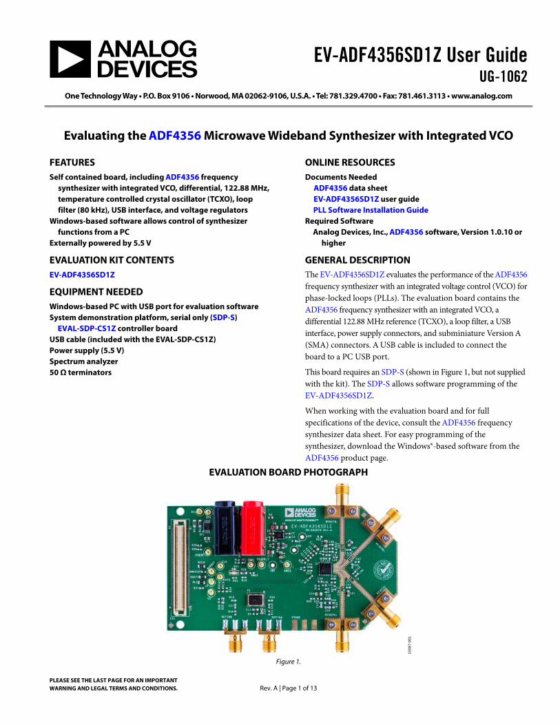
GENERAL DESCRIPTION The EV-ADF4356SD1Z evaluates the performance of the ADF4356 frequency synthesizer with an integrated voltage control (VCO) for phase-locked loops (PLLs). The evaluation board contains the ADF4356 frequency synthesizer with an integrated VCO, a differential 122.88 MHz reference (TCXO), a loop filter, a USB interface, power supply connectors, and subminiature Version A (SMA) connectors. A USB cable is included to connect the board to a PC USB port.
This board requires an SDP-S (shown in Figure 1, but not supplied with the kit). The SDP-S allows software programming of the EV-ADF4356SD1Z.
When working with the evaluation board and for full specifications of the device, consult the ADF4356 frequency synthesizer data sheet. For easy programming of the synthesizer, download the Windows®-based software from the ADF4356 product page.
EVALUATION BOARD PHOTOGRAPH
1508
7-00
1
Figure 1.
UG-1062 EV-ADF4356SD1Z User Guide
Rev. A | Page 2 of 13
TABLE OF CONTENTS Features .............................................................................................. 1 Evaluation Kit Contents ................................................................... 1 Equipment Needed ........................................................................... 1 Online Resources .............................................................................. 1 General Description ......................................................................... 1 Evaluation Board Photograph ......................................................... 1 Revision History ............................................................................... 2 Getting Started .................................................................................. 3
Software Installation Procedures ................................................ 3 Evaluation Board Setup Procedures ........................................... 3
Evaluation Board Hardware ............................................................ 4 Power Supplies .............................................................................. 4
RF Output .......................................................................................4 Loop Filter ......................................................................................4 Reference Source ...........................................................................4 Default Configuration ..................................................................4 Evaluation Board Setup ................................................................5
Evaluation Board Software ...............................................................6 Main Controls ................................................................................6
Evaluation and Test ...........................................................................7 Evaluation Board Schematics and Artwork ...................................8 Ordering Information .................................................................... 12
Bill of Materials ........................................................................... 12
REVISION HISTORY 04/2017—Rev. 0 to Rev. A
Changes to Features, Evaluation Kit Contents, Equipment Needed, Online Resources Sections, and Figure 1 ....................... 1 Changes to Figure 2 .......................................................................... 3 Changes to Evaluation Board Hardware Section and Deleted Figure 3, Renumbered Sequentially ............................................... 4 Changes to Figure 3 .......................................................................... 5 Changes to Evaluation Board Software, Step 5 and Figure 5 ...... 7 Changes to Figure 6 .......................................................................... 8 Changes to Figure 7 .......................................................................... 9 Deleted Figure 8, Renumbered Sequentially ................................. 9 Changes to Figure 8, Figure 9, and Figure 10 ............................. 10 Deleted Figure 11, Renumbered Sequentially ............................. 11 Changes to Figure 11 ...................................................................... 11 Changes to Figure 12 ...................................................................... 12 Changes to Table 1 .......................................................................... 13
10/2016—Revision 0: Initial Version
EV-ADF4356SD1Z User Guide UG-1062
Rev. A | Page 3 of 13
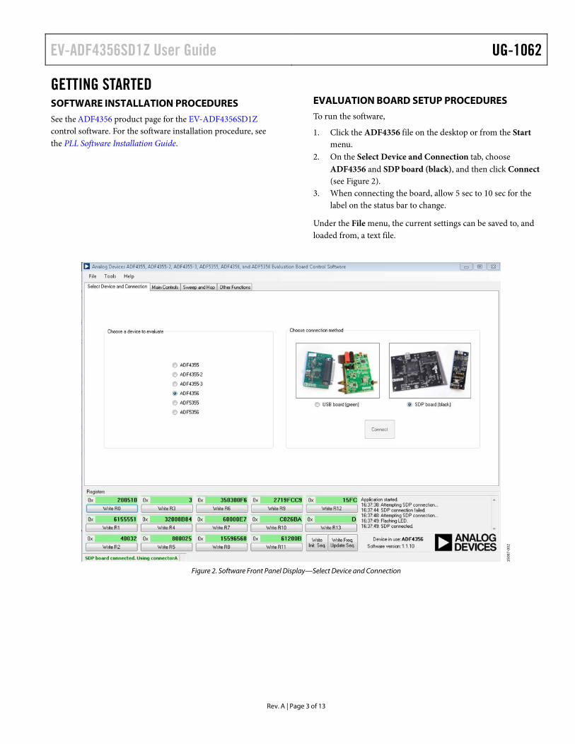
GETTING STARTED SOFTWARE INSTALLATION PROCEDURES See the ADF4356 product page for the EV-ADF4356SD1Z control software. For the software installation procedure, see the PLL Software Installation Guide.
EVALUATION BOARD SETUP PROCEDURES To run the software,
1. Click the ADF4356 file on the desktop or from the Start menu.
2. On the Select Device and Connection tab, choose ADF4356 and SDP board (black), and then click Connect (see Figure 2).
3. When connecting the board, allow 5 sec to 10 sec for the label on the status bar to change.
Under the File menu, the current settings can be saved to, and loaded from, a text file.
1508
7-00
2
Figure 2. Software Front Panel Display—Select Device and Connection
UG-1062 EV-ADF4356SD1Z User Guide
Rev. A | Page 4 of 13
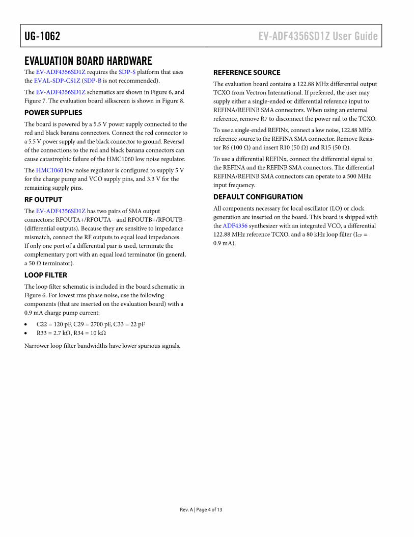
EVALUATION BOARD HARDWARE The EV-ADF4356SD1Z requires the SDP-S platform that uses the EVAL-SDP-CS1Z (SDP-B is not recommended).
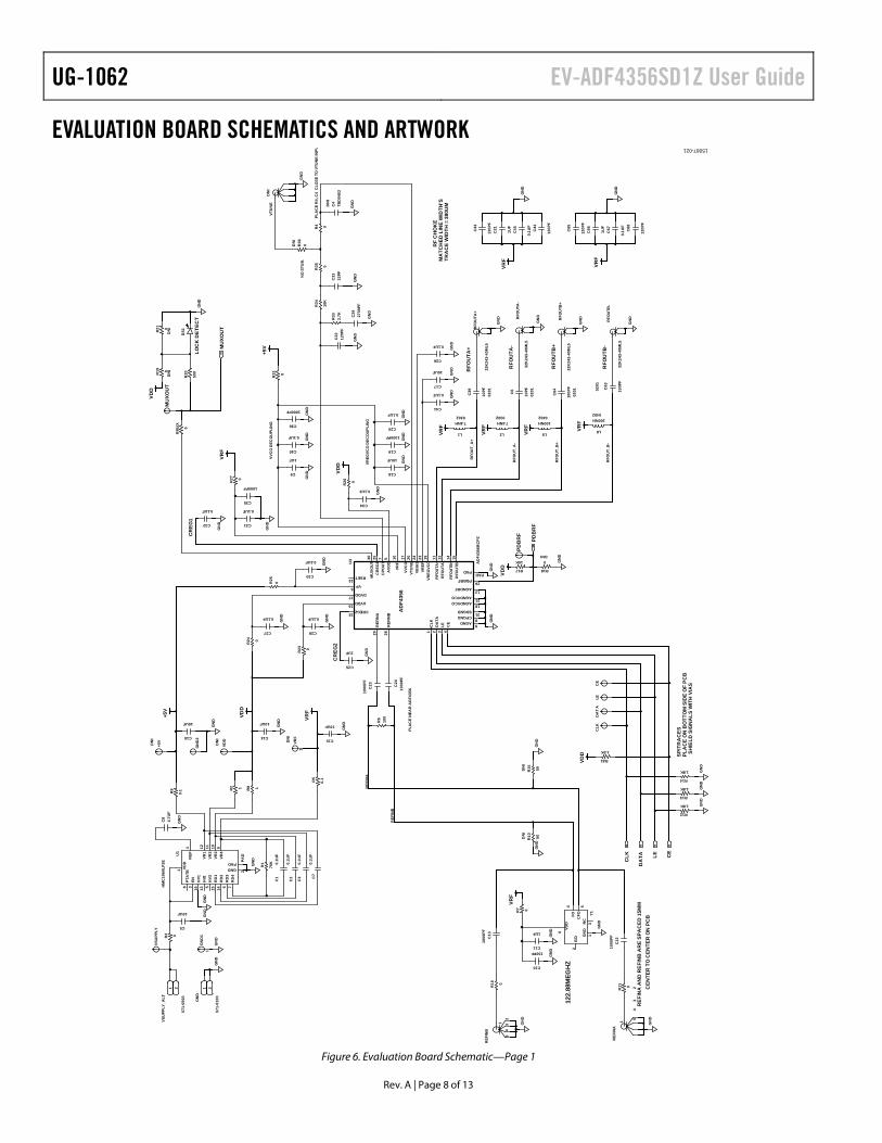
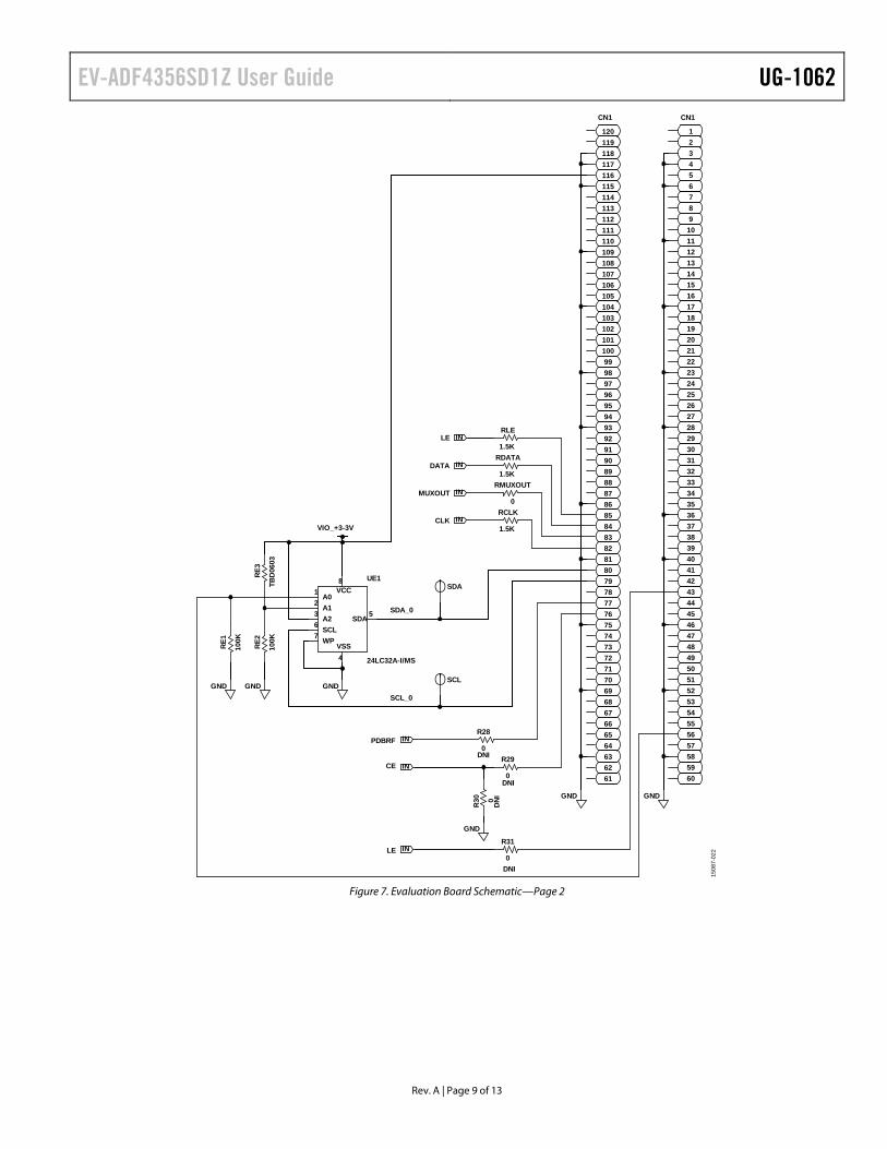
The EV-ADF4356SD1Z schematics are shown in Figure 6, and Figure 7. The evaluation board silkscreen is shown in Figure 8.
POWER SUPPLIES The board is powered by a 5.5 V power supply connected to the red and black banana connectors. Connect the red connector to a 5.5 V power supply and the black connector to ground. Reversal of the connections to the red and black banana connectors can cause catastrophic failure of the HMC1060 low noise regulator.
The HMC1060 low noise regulator is configured to supply 5 V for the charge pump and VCO supply pins, and 3.3 V for the remaining supply pins.
RF OUTPUT The EV-ADF4356SD1Z has two pairs of SMA output connectors: RFOUTA+/RFOUTA− and RFOUTB+/RFOUTB− (differential outputs). Because they are sensitive to impedance mismatch, connect the RF outputs to equal load impedances. If only one port of a differential pair is used, terminate the complementary port with an equal load terminator (in general, a 50 Ω terminator).
LOOP FILTER The loop filter schematic is included in the board schematic in Figure 6. For lowest rms phase noise, use the following components (that are inserted on the evaluation board) with a 0.9 mA charge pump current:
• C22 = 120 pF, C29 = 2700 pF, C33 = 22 pF • R33 = 2.7 kΩ, R34 = 10 kΩ
Narrower loop filter bandwidths have lower spurious signals.
REFERENCE SOURCE The evaluation board contains a 122.88 MHz differential output TCXO from Vectron International. If preferred, the user may supply either a single-ended or differential reference input to REFINA/REFINB SMA connectors. When using an external reference, remove R7 to disconnect the power rail to the TCXO.
To use a single-ended REFINx, connect a low noise, 122.88 MHz reference source to the REFINA SMA connector. Remove Resis-tor R6 (100 Ω) and insert R10 (50 Ω) and R15 (50 Ω).
To use a differential REFINx, connect the differential signal to the REFINA and the REFINB SMA connectors. The differential REFINA/REFINB SMA connectors can operate to a 500 MHz input frequency.
DEFAULT CONFIGURATION All components necessary for local oscillator (LO) or clock generation are inserted on the board. This board is shipped with the ADF4356 synthesizer with an integrated VCO, a differential 122.88 MHz reference TCXO, and a 80 kHz loop filter (ICP = 0.9 mA).
EV-ADF4356SD1Z User Guide UG-1062
Rev. A | Page 5 of 13
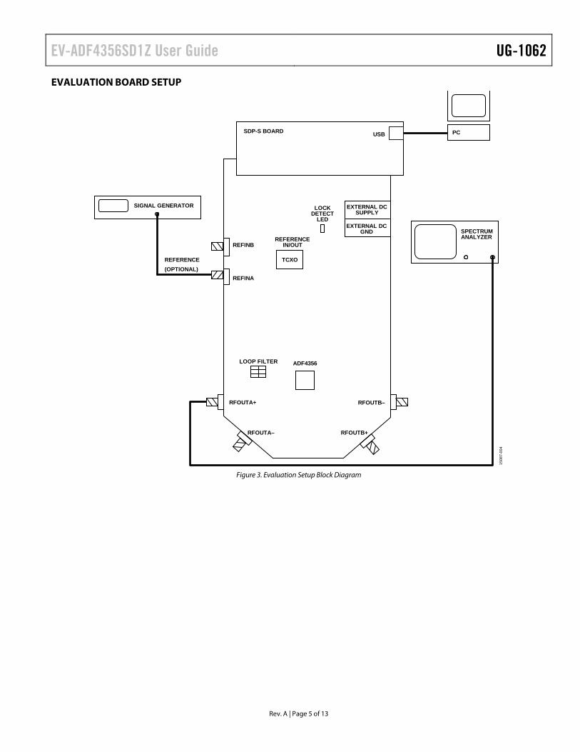
EVALUATION BOARD SETUP
SPECTRUMANALYZER
PC
EXTERNAL DCSUPPLY
TCXO
ADF4356LOOP FILTER
LOCKDETECT
LED
REFERENCEIN/OUT
SDP-S BOARD
REFINA
REFINB
RFOUTB–
RFOUTA–
RFOUTA+
RFOUTB+
REFERENCE(OPTIONAL)
SIGNAL GENERATOR
EXTERNAL DCGND
USB
1508
7-00
4
Figure 3. Evaluation Setup Block Diagram
UG-1062 EV-ADF4356SD1Z User Guide
Rev. A | Page 6 of 13
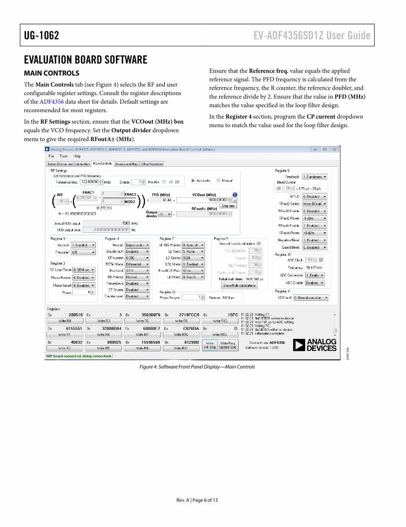
EVALUATION BOARD SOFTWARE MAIN CONTROLS The Main Controls tab (see Figure 4) selects the RF and user configurable register settings. Consult the register descriptions of the ADF4356 data sheet for details. Default settings are recommended for most registers.
In the RF Settings section, ensure that the VCOout (MHz) box equals the VCO frequency. Set the Output divider dropdown menu to give the required RFoutA± (MHz).
Ensure that the Reference freq. value equals the applied reference signal. The PFD frequency is calculated from the reference frequency, the R counter, the reference doubler, and the reference divide by 2. Ensure that the value in PFD (MHz) matches the value specified in the loop filter design.
In the Register 4 section, program the CP current dropdown menu to match the value used for the loop filter design.
1508
7-00
5
Figure 4. Software Front Panel Display—Main Controls
EV-ADF4356SD1Z User Guide UG-1062
Rev. A | Page 7 of 13
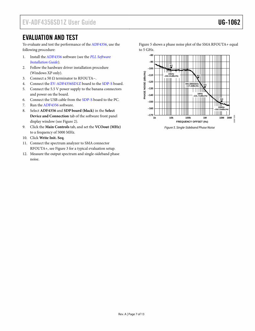
EVALUATION AND TEST To evaluate and test the performance of the ADF4356, use the following procedure:
1. Install the ADF4356 software (see the PLL Software Installation Guide).
2. Follow the hardware driver installation procedure (Windows XP only).
3. Connect a 50 Ω terminator to RFOUTA−. 4. Connect the EV-ADF4356SD1Z board to the SDP-S board. 5. Connect the 5.5 V power supply to the banana connectors
and power on the board. 6. Connect the USB cable from the SDP-S board to the PC. 7. Run the ADF4356 software. 8. Select ADF4356 and SDP board (black) in the Select
Device and Connection tab of the software front panel display window (see Figure 2).
9. Click the Main Controls tab, and set the VCOout (MHz) to a frequency of 5000 MHz.
10. Click Write Init. Seq. 11. Connect the spectrum analyzer to SMA connector
RFOUTA+, see Figure 3 for a typical evaluation setup. 12. Measure the output spectrum and single-sideband phase
noise.
Figure 5 shows a phase noise plot of the SMA RFOUTA+ equal to 5 GHz.
–80
–170
–160
–150
–140
–130
–120
–110
–100
–90
1k 10k 100k 1M 10M 30M
PHA
SE N
OIS
E (d
Bc/
Hz)
FREQUENCY OFFSET (Hz) 1508
7-02
0
M1
M2
M3
M4
10kHz–102.41dBc/Hz
400.39063kHz–117.2dBc/Hz
1MHz–131.71dBc/Hz
10MHz–152.33dBc/Hz
Figure 5. Single-Sideband Phase Noise
UG-1062 EV-ADF4356SD1Z User Guide
Rev. A | Page 8 of 13
EVALUATION BOARD SCHEMATICS AND ARTWORK
15087-021
PLA
CE
NEA
R A
DF4
356
VREG
VCO
DEC
OU
PLIN
G
VVC
O D
ECO
UPL
ING
CEN
TER
TO
CEN
TER
ON
PC
B
MA
TCH
ED L
INE
WID
TH'S
TRA
CE
WID
TH =
380
UM
RF
CH
OK
E
0201
0302
0201 02
01
0201
0402
AD
F435
6
SHIE
LD S
IGN
ALS
WIT
H V
IAS
PLA
CE
ON
BO
TTO
M S
IDE
OF
PCB
SPIT
RA
CES
LOC
K D
ETEC
T
0302
REF
INA
AN
D R
EFIN
B A
RE
SPA
CED
15M
M
0402
NO
STU
B.
PLA
CE
R4,
C4
CLO
SE T
O V
TUN
E IN
PU
DN
I
122.
88M
EGH
Z
32K
243-
40M
L5
DN
I
0.1UF
1000PF
22PF
0
1
0.1U
F
DN
I
0.1UF
0
0
100PF
0
0
0
0DNI
10K
32K
243-
40M
L5
0
0DN
I
120P
F
0
1000PF
0.1UF
0
0
0D
NI
0D
NI
0
0
10UF
0.1UF
0.1UF
1UF
2700
PF
0.1UF
DN
I
DN
I
10UF
AD
F435
6BC
PZ
10UF10UF
0.1
0.1
0.1U
F
0.1U
F
75K
HM
C10
60LP
3E
50
571-
0100
571-
0500
4.7U
F
DN
I
120P
F
120P
F
120P
F
120P
F
100NH100NH
1000
PF
1000
PF
7.4NH
0.1U
F
0.1U
F
1.8K
1.8K
1.8K
1UF
1UF
32K
243-
40M
L5
32K
243-
40M
L5
10PF
10PF
100P
F
100P
F
TBD
0402
7.4NH
1.5K
50
1UF
100
500
1UF
0.1U
F
DN
I
1000
PF
1000
PF
0.1UF
0.1UF
10UF
0.1UF
1000PF
1
10UF
0.1UF
0
2.7K
10K
R27
R32
R25
R34
R33 C
29
C33
C22
C9
C20
C18
C19
R24
C4
R23
R26
R36
R35
VRF
GN
D1
R6
C8
R5
R1
R2
C7
C3
C2
C1
U1
VSU
PPLY
_ALT GN
D
CE
R22
GN
D2
U3
C39
R9
C30
C12
C13
C35
C36
R8
C17
C34
R15
R10
C40
C41
C31
+5V
VDD C15
C16 C14
VSU
PPLY
C5
R3
VTU
NE
REF
INB
REF
INA
C68
C67
C66C65
C63
C64
L5L8
RFO
UTB
-
R4
C26
C6
L1
C21
C24
C23
L2
C28
C25
C32
DA
TA
LEC
LK
RM
UX
R20
RFO
UTB
+
RFO
UTA
-
RFO
UTA
+
R18
C27
R17
PDB
RF
R11
Y1
R16
C10
C44
C45C43
R12
R13
R14
C11
R7
MU
XOU
T
R19
DS1R
21
REF
INB
REF
INA
VRF
RFO
UT_
A-
VDD
VRF
+5V
CR
EG1
RFO
UT_
A+
VDD
DA
TA
VDD
CLK
RFO
UT_
B-
RFO
UT_
B+
VRF
VRF
LE
VDD
VRF
VRF
RFO
UTA
-
RFO
UTB
-
CE
VRF
RFO
UTA
+
VRF
CR
EG2
+5V
VDD
MU
XOU
T
VRF
PDB
RF
RFO
UTB
+
1
1
9101112
1
4
7614158
PAD
51316
2
3
21 21
17 2010 1923
6
24
31
22
15141211
2829
26
PAD
30
3
27
2
32
25 7
8
1 4
16
5
2118
13
9
15
43
2 54
32
1
6
42
5
13
GN
D
GN
D
GN
D
GN
D
VDD
CFOFO
GN
D
E/D
NC
GN
D
GN
D
GN
D
GN
D
GN
DG
ND
GN
D
GN
D
GN
D
GN
D
GN
D
GN
D
PAD
HV1
RD
1R
D2
HV2
VR1
VR2
VR3
VR4
PTA
TB
RD
4R
D3
HV3
REF
EN
GNDVDD
GN
D
GN
D
GN
D
PAD
AGNDVCOAGNDVCO
AGNDRF
AVDD
AVD
D
CREG2 SDGND
MU
XOU
TR
EFIN
A
REF
INB
DVDD
PDBRF
CR
EG1
VBIA
SVR
EF
RSET VTU
NE
VREG
VCO
VVC
O
RFO
UTB
-R
FOU
TB+
RFO
UTA
-R
FOU
TA+
VRF
AGNDCPGND
CPO
UT
VP
CE
LEDA
TAC
LK
GN
D
GN
D
GN
D
GN
DG
ND
GN
D
GN
D
GN
D
GN
D
GN
D
GN
D
GN
D
GN
D
GN
D
GN
D
GN
D
GN
D
GN
DGN
D
IN
IN
ININININ
GN
D
GN
D
GN
DG
ND
GN
DG
ND
GN
D
GN
D
GN
D
GN
D
GN
D
GN
D
Figure 6. Evaluation Board Schematic—Page 1
EV-ADF4356SD1Z User Guide UG-1062
Rev. A | Page 9 of 13
1508
7-02
2
1.5K
0
1.5K
TBD
0603
0
0DNI
0
24LC32A-I/MS
DN
I
100K
DNI
1.5K
100K
DNI0
R31
R30
R29
R28
SDA
SCL
RMUXOUT
RDATA
RLE
RCLK
RE3
RE2
RE1
UE1
CN1CN1
CLK
MUXOUT
DATA
VIO_+3-3V
PDBRF
SCL_0
SDA_0
CE
LE
LE
7
4
8
56321
605958575655545352515049484746454443424140393837363534333231302928272625242322212019181716151413121110987654321
616263646566676869707172737475767778798081828384858687888990919293949596979899
100101102103104105106107108109110111112113114115116117118119120
IN
IN
IN
IN
IN
IN
IN
GND
GND GND GND
VSS
VCC
WP
A2A1A0
SCLSDA
GNDGND
Figure 7. Evaluation Board Schematic—Page 2
UG-1062 EV-ADF4356SD1Z User Guide
Rev. A | Page 10 of 13
1508
7-02
3
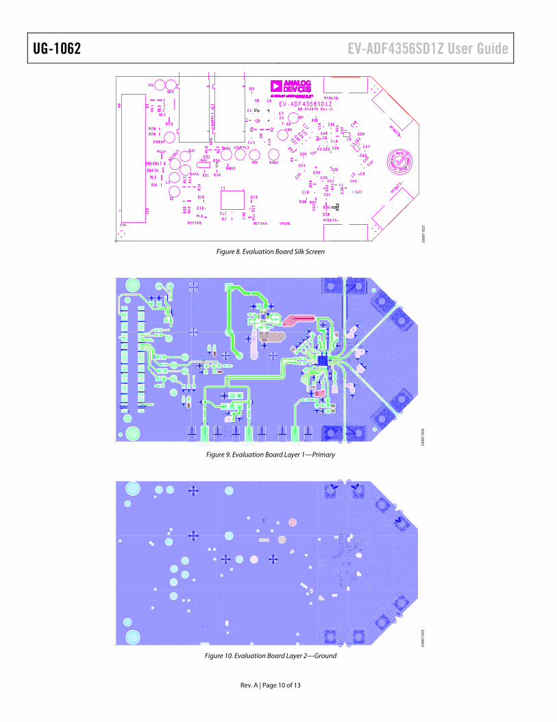
Figure 8. Evaluation Board Silk Screen
1508
7-02
4
Figure 9. Evaluation Board Layer 1—Primary
1508
7-02
5
Figure 10. Evaluation Board Layer 2—Ground
EV-ADF4356SD1Z User Guide UG-1062
Rev. A | Page 11 of 13
1508
7-02
6
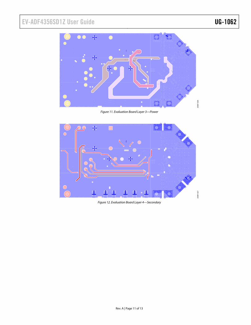
Figure 11. Evaluation Board Layer 3—Power
1508
7-02
7
Figure 12. Evaluation Board Layer 4—Secondary
UG-1062 EV-ADF4356SD1Z User Guide
Rev. A | Page 12 of 13
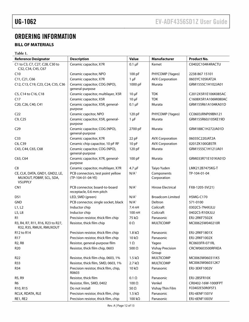
ORDERING INFORMATION BILL OF MATERIALS
Table 1. Reference Designator Description Value Manufacturer Product No. C1 to C3, C7, C27, C28, C30 to
C32, C34, C45, C67 Ceramic capacitor, X7R 0.1 μF Kemet C0402C104K4RACTU
C10 Ceramic capacitor, NPO 100 pF PHYCOMP (Yageo) 2238 867 15101 C11, C21, C66 Ceramic capacitor, X7R 1 μF AVX Corporation 0603YC105KAT2A C12, C13, C19, C23, C24, C35, C36 Ceramic capacitor, COG (NPO),
general-purpose 1000 pF Murata GRM1555C1H102JA01
C5, C14 to C16, C18 Ceramic capacitor, multilayer, X5R 10 μF TDK C2012X5R1E106K085AC C17 Ceramic capacitor, X5R 10 μF TDK C1608X5R1A106M080AC C20, C26, C40, C41 Ceramic capacitor, X5R, general-
purpose 0.1 μF Murata GRM155R61A104KA01D
C22 Ceramic capcitor, NPO 120 pF PHYCOMP (Yageo) CC0603JRNP09BN121 C9, C25 Ceramic capacitor, X5R, general-
purpose 1 μF Murata GRM155R60J105KE19D
C29 Ceramic capacitor, COG (NPO), general-purpose
2700 pF Murata GRM188C1H272JA01D
C33 Ceramic capacitor, X7R 22 pF AVX Corporation 06035C220JAT2A C6, C39 Ceramic chip capacitor, 10 pF RF 10 pF AVX Corporation 0201ZK100GBSTR C43, C44, C65, C68 Ceramic capacitor, COG (NPO),
general-purpose 120 pF Murata GRM1555C1H121JA01
C63, C64 Ceramic capacitor, X7R, general-purpose
100 pF Murata GRM033R71E101KA01D
C8 Ceramic capacitor, multilayer, X7R 4.7 μF Taiyo Yuden LMK212B7475KG-T CE, CLK, DATA, GND1, GND2, LE,
MUXOUT, PDBRF, SCL, SDA, VSUPPLY
PCB connectors, test point yellow (TP-104-01-04-YE)
N/A1 Components Corporation
TP-104-01-04
CN1 PCB connector, board-to-board receptacle, 0.6 mm pitch
N/A1 Hirose Electrical FX8-1205-5V(21)
DS1 LED, SMD (green) N/A1 Broadcom Limited HSMG-C170 GND PCB connector, single socket, black N/A1 Deltron 571-0100 L1, L2 Inductor chip 7.4 nH Coilcraft 0302CS-7N4XJLU L5, L8 Inductor chip 100 nH Coilcraft 0402CS-R10XJLU R1 Precision resistor, thick film chip 75 kΩ Panasonic ERJ-2RKF7502X R3, R4, R7, R11, R16, R23 to R27,
R32, R35, RMUX, RMUXOUT Resistor, thick film chip 0 Ω MULTICOMP MC00625W040210R
R12 to R14 Precision resistor, thick film chip 1.8 kΩ Panasonic ERJ-2RKF1801X R17 Precision resistor, thick film chip 10 kΩ Panasonic ERJ-2RKF1002X R2, R8 Resistor, general-purpose film 1 Ω Yageo RC0603FR-071RL R20 Resistor, thick film chip, 0603 500 Ω Vishay Precision
Group CRCW0603500RFKEA
R22 Resistor, thick film chip, 0603, 1% 1.5 kΩ MULTICOMP MC0063W060311K5 R33 Resistor, thick film, SMD, 0603, 1% 2.7 kΩ MULTICOMP MC0063W060312K7
R34 Precision resistor, thick film, chip, R0603
10 kΩ Panasonic ERJ-3EKF1002V
R5, R9 Resistor, thick film 0.1 Ω Panasonic ERJ-2BSFR10X R6 Resistor, film, SMD, 0402 100 Ω Venkel CR0402-16W-1000FPT R10, R15 Do not install 50 Ω Vishay Thin Film FC0402E50R0FST1 RCLK, RDATA, RLE Precision resistor, thick film, chip 1.5 kΩ Panasonic ERJ-6ENF1501V RE1, RE2 Precision resistor, thick film, chip 100 kΩ Panasonic ERJ-6ENF1003V
EV-ADF4356SD1Z User Guide UG-1062
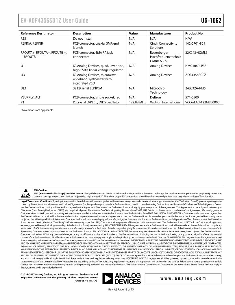
Rev. A | Page 13 of 13
Reference Designator Description Value Manufacturer Product No. RE3 Do not install N/A1 N/A1 N/A1 REFINA, REFINB PCB connector, coaxial SMA end
launch N/A1 Cinch Connectivity
Solutions 142-0701-801
RFOUTA+, RFOUTA−, RFOUTB +, RFOUTB−
PCB connector, SMA RA jack connectors
N/A1 Rosenberger Hochfrequenztechnik GMBH & Co.
32K243-4OML5
U1 IC, Analog Devices, quad, low noise, high PSRR, linear voltage regulator
N/A1 Analog Devices HMC1060LP3E
U3 IC, Analog Devices, microwave wideband synthesizer with integrated VCO
N/A1 Analog Devices ADF4356BCPZ
UE1 32 kB serial EEPROM N/A1 Microchip Technology
24LC32A-I/M5
VSUPPLY_ALT PCB connector, single socket, red N/A1 Deltron 571-0500 Y1 IC crystal LVPECL, LVDS oscillator 122.88 MHz Vectron International VCC6-LAB-122M880000 1 N/A means not applicable.
ESD Caution ESD (electrostatic discharge) sensitive device. Charged devices and circuit boards can discharge without detection. Although this product features patented or proprietary protection circuitry, damage may occur on devices subjected to high energy ESD. Therefore, proper ESD precautions should be taken to avoid performance degradation or loss of functionality.
Legal Terms and Conditions By using the evaluation board discussed herein (together with any tools, components documentation or support materials, the “Evaluation Board”), you are agreeing to be bound by the terms and conditions set forth below (“Agreement”) unless you have purchased the Evaluation Board, in which case the Analog Devices Standard Terms and Conditions of Sale shall govern. Do not use the Evaluation Board until you have read and agreed to the Agreement. Your use of the Evaluation Board shall signify your acceptance of the Agreement. This Agreement is made by and between you (“Customer”) and Analog Devices, Inc. (“ADI”), with its principal place of business at One Technology Way, Norwood, MA 02062, USA. Subject to the terms and conditions of the Agreement, ADI hereby grants to Customer a free, limited, personal, temporary, non-exclusive, non-sublicensable, non-transferable license to use the Evaluation Board FOR EVALUATION PURPOSES ONLY. Customer understands and agrees that the Evaluation Board is provided for the sole and exclusive purpose referenced above, and agrees not to use the Evaluation Board for any other purpose. Furthermore, the license granted is expressly made subject to the following additional limitations: Customer shall not (i) rent, lease, display, sell, transfer, assign, sublicense, or distribute the Evaluation Board; and (ii) permit any Third Party to access the Evaluation Board. As used herein, the term “Third Party” includes any entity other than ADI, Customer, their employees, affiliates and in-house consultants. The Evaluation Board is NOT sold to Customer; all rights not expressly granted herein, including ownership of the Evaluation Board, are reserved by ADI. CONFIDENTIALITY. This Agreement and the Evaluation Board shall all be considered the confidential and proprietary information of ADI. Customer may not disclose or transfer any portion of the Evaluation Board to any other party for any reason. Upon discontinuation of use of the Evaluation Board or termination of this Agreement, Customer agrees to promptly return the Evaluation Board to ADI. ADDITIONAL resistorTRICTIONS. Customer may not disassemble, decompile or reverse engineer chips on the Evaluation Board. Customer shall inform ADI of any occurred damages or any modifications or alterations it makes to the Evaluation Board, including but not limited to soldering or any other activity that affects the material content of the Evaluation Board. Modifications to the Evaluation Board must comply with applicable law, including but not limited to the RoHS Directive. TERMINATION. ADI may terminate this Agreement at any time upon giving written notice to Customer. Customer agrees to return to ADI the Evaluation Board at that time. LIMITATION OF LIABILITY. THE EVALUATION BOARD PROVIDED HEREUNDER IS PROVIDED “AS IS” AND ADI MAKES NO WARRANTIES OR REPresistorENTATIONS OF ANY KIND WITH resistorPECT TO IT. ADI SPECIFICALLY DISCLAIMS ANY REPresistorENTATIONS, ENDORSEMENTS, GUARANTEES, OR WARRANTIES, EXPresistorS OR IMPLIED, RELATED TO THE EVALUATION BOARD INCLUDING, BUT NOT LIMITED TO, THE IMPLIED WARRANTY OF MERCHANTABILITY, TITLE, FITNESS FOR A PARTICULAR PURPOSE OR NONINFRINGEMENT OF INTELLECTUAL PROPERTY RIGHTS. IN NO EVENT WILL ADI AND ITS LICENSORS BE LIABLE FOR ANY INCIDENTAL, SPECIAL, INDIRECT, OR CONSEQUENTIAL DAMAGES resistorULTING FROM CUSTOMER’S POSSESSION OR USE OF THE EVALUATION BOARD, INCLUDING BUT NOT LIMITED TO LOST PROFITS, DELAY COSTS, LABOR COSTS OR LOSS OF GOODWILL. ADI’S TOTAL LIABILITY FROM ANY AND ALL CAUSES SHALL BE LIMITED TO THE AMOUNT OF ONE HUNDRED US DOLLARS ($100.00). EXPORT. Customer agrees that it will not directly or indirectly export the Evaluation Board to another country, and that it will comply with all applicable United States federal laws and regulations relating to exports. GOVERNING LAW. This Agreement shall be governed by and construed in accordance with the substantive laws of the Commonwealth of Massachusetts (excluding conflict of law rules). Any legal action regarding this Agreement will be heard in the state or federal courts having jurisdiction in Suffolk County, Massachusetts, and Customer hereby submits to the personal jurisdiction and venue of such courts. The United Nations Convention on Contracts for the International Sale of Goods shall not apply to this Agreement and is expressly disclaimed.
©2016–2017 Analog Devices, Inc. All rights reserved. Trademarks and registered trademarks are the property of their respective owners. UG15087-0-4/17(A)