Embed Size (px)
Citation preview
Duke University Department of Electrical and Computer Engineering
Technical Report Duke-ECE-2013-6-5, June 5, 2013
Evaluating Cache Coherent Shared Virtual Memory for Heterogeneous Multicore Chips BLAKE A. HECHTMAN, Duke University DANIEL J. SORIN, Duke University
The trend in industry is towards heterogeneous multicore processors (HMCs), including chips with
CPUs and massively-threaded throughput-oriented processors (MTTOPs) such as GPUs.
Although current homogeneous chips tightly couple the cores with cache-coherent shared virtual
memory (CCSVM), this is not the communication paradigm used by any current HMC. In this
paper, we present a CCSVM design for a CPU/MTTOP chip, as well as an extension of the
pthreads programming model, called xthreads, for programming this HMC. Our goal is to
evaluate the potential performance benefits of tightly coupling heterogeneous cores with CCSVM.
1 INTRODUCTION
The trend in general-purpose chips is for them to consist of multiple cores of various types—
including traditional, general-purpose compute cores (CPU cores), graphics cores (GPU cores),
digital signal processing cores (DSPs), cryptography engines, etc.—connected to each other and to
a memory system. Already, general-purpose chips from major manufacturers include CPU and
GPU cores, including Intel’s Sandy Bridge [42][16], AMD’s Fusion [4], and Nvidia Research’s
Echelon [18]. IBM’s PowerEN chip [3] includes CPU cores and four special-purpose cores,
including accelerators for cryptographic processing and XML processing.
In Section 2, we compare current heterogeneous multicores to current homogeneous
multicores, and we focus on how the cores communicate with each other. Perhaps surprisingly, the
communication paradigms in emerging heterogeneous multicores (HMCs) differ from the
established, dominant communication paradigm for homogeneous multicores. The vast majority
of homogeneous multicores provide tight coupling between cores, with all cores communicating
and synchronizing via cache-coherent shared virtual memory (CCSVM). Despite the benefits of
tight coupling, current HMCs are loosely coupled and do not support CCSVM, although some
HMCs support aspects of CCSVM.
In Section 3, we develop a tightly coupled CCSVM architecture and microarchitecture for an
HMC consisting of CPU cores and massively-threaded throughput-oriented processor (MTTOP)
cores.1 The most prevalent examples of MTTOPs are GPUs, but MTTOPs also include Intel’s
Many Integrated Core (MIC) architecture [31] and academic accelerator designs such as Rigel
[19] and vector-thread architectures [21]. The key features that distinguish MTTOPs from CPU
multicores are: a very large number of cores, relatively simple core pipelines, hardware support for
a large number of threads per core, and support for efficient data-parallel execution using the
SIMT execution model.
We do not claim to invent CCSVM for HMCs; rather our goal is to evaluate one strawman
design in this space. As a limit study of CCSVM for HMCs, we prefer an extremely tightly
coupled design instead of trying to more closely model today’s HMC chips. We discuss many of
the issues that arise when designing CCSVM for HMCs, including TLB misses at MTTOP cores
and maintaining TLB coherence.
In Section 4, we present a programming model that we have developed for utilizing CCSVM
on an HMC. The programming model, called xthreads, is a natural extension of pthreads. In the
xthreads programming model, a process running on a CPU can spawn a set of threads on MTTOP
cores in a way that is similar to how one can spawn threads on CPU cores using pthreads. We
have implemented the xthreads compilation toolchain to automatically convert xthreads source
code into executable code for the CPUs and MTTOPs.
In Section 5, we present an experimental evaluation of our HMC design and the performance of
xthreads software running on it. The evaluation compares our full-system simulation of an HMC
1 We use the term “GPU core” to refer to a streaming multiprocessor (SM) in NVIDIA terminology or a
compute unit in AMD terminology.

2
with CCSVM to a high-end HMC currently on the market from AMD. We show that the CCSVM
HMC can vastly outperform the AMD chip when offloading small tasks from the CPUs to the
MTTOPs.
In Section 6, we discuss the open challenges in supporting CCSVM on future HMCs. We have
demonstrated the potential of CCSVM to improve performance and efficiency, but there are still
issues to resolve, including scalability and maintaining performance on graphics workloads.
In Section 7, we discuss related work, including several recent HMC designs.
In this paper, we make the following contributions:
• We describe the architecture and microarchitecture for an HMC with CCSVM,
• We explain the differences between an HMC with CCSVM and state-of-the-art systems,
• We experimentally demonstrate the potential of an HMC with CCSVM to increase
performance and reduce the number of off-chip DRAM accesses, compared to a state-of-
the-art HMC running OpenCL, and
• We show how CCSVM/xthreads enables the use of pointer-based data structures in
software that runs on CPU/MTTOP chips, thus extending MTTOP applications from
primarily numerical code to include pointer-chasing code.
2 Communication Paradigms for Current Multicore Chips
In this section, we compare the tightly-coupled designs of current homogeneous multicores to
the loosely-coupled designs of current heterogeneous multicores. At the end of this section, we
focus on one representative heterogeneous multicore, AMD’s Llano Fusion APU [4]2; we use the
APU as the system we experimentally compare against in Section 5. We defer a discussion of
other HMCs until Section 7.
2.1 Homogeneous Multicore Chips
The vast majority of today’s homogeneous chips [32][23][34][7], including homogeneous chips
with vector units [31], tightly couple the cores with hardware-implemented, fine-grained, cache-
coherent shared virtual memory (CCSVM). The virtual memory is managed by the operating
system’s kernel and easily shared between threads. Hardware cache coherence provides automatic
data movement between cores and removes this burden from the programmer. Although there are
some concerns about coherence’s scalability, recent work shows that coherence should scale to at
least hundreds of cores [28].
By coupling the cores together very tightly, CCSVM offers many attractive features. Tightly-
coupled multicore chips have relatively low overheads for communication and synchronization.
CCSVM enables software to be highly portable in both performance and functionality. It is also
easy to launch threads on homogeneous CPUs since the kernel manages threads and schedules
them intelligently.
2.2 Communication Options for Heterogeneous Multicore Chips
The most important design decision in a multicore chip is choosing how the cores should
communicate. Even though the dominant communication paradigm in today’s homogeneous
chips is CCSVM, no existing HMC uses CCSVM. AMD, ARM, and Qualcomm have
collaborated to create an architecture called HSA that provides shared virtual memory and a
memory consistency model, yet HSA does not provide coherence [39]. Some chips, such as the
Cell processor [17] and a recent ARM GPU3, provide shared virtual memory but without hardware
cache coherence. AMD also suggests that future GPUs may have hardware support for address
translation [1]. Other HMC designs provide software-implemented coherent shared virtual
memory at the programming language level [20][13]. Another common design is for the cores to
communicate via DMA, thus communicating large quantities of data (i.e., coarse-grain
communication) from one memory to another. These memories may or may not be part of the
2 We would have also considered Intel’s SandyBridge CPU/GPU chip [42], but there is insufficient publicly
available information on it for us to confidently describe its design. 3 http://blogs.arm.com/multimedia/534-memory-management-on-embedded-graphics-processors/
3
same virtual address space, depending on the chip design. The DMA transfer may or may not
maintain cache coherence.
The options for synchronizing between CPU cores and non-CPU cores are closely related to the
communication mechanisms. Communication via DMA often leads to synchronization via
interrupts and/or polling through memory-mapped I/O. Communication via CCSVM facilitates
synchronization via atomic operations (e.g., fetch-and-op) and memory barriers.
2.3 A Typical HMC: The AMD Fusion APU
AMD’s current Fusion APU, code-named Llano [11], is a heterogeneous multicore processor
consisting of x86-64 CPU cores and a Radeon GPU. The CPU and GPU cores have different
virtual address spaces, but they can communicate via regions of physical memory that are pinned
in known locations. The chip has a unified Northbridge that, under some circumstances, facilitates
coherent communication across these virtual address spaces. Llano supports multiple
communication paradigms. First, Llano permits the CPU cores and the GPU to perform coherent
DMA between their virtual address spaces. In a typical OpenCL program, the CPU cores use
DMA to transfer the input data to the GPU, and the GPU’s driver uses DMA to transfer the output
data back to the CPU cores. Although the DMA transfers are coherent with respect to the CPU’s
caches, the load/store accesses by CPU cores and GPU cores between the DMA accesses are not
coherent. Second, Llano allows a CPU core to perform high-bandwidth, uncacheable writes
directly into part of the GPUs’ virtual address space that is pinned in physical memory at boot.
Third, Llano introduces the Fusion Control Link (FCL) that provides coherent communication
over the Unified NorthBridge (UNB) but at a lower bandwidth. With FCL, the GPU driver can
create a shared memory region in pinned physical memory that is mapped in both the CPU and
GPU virtual address spaces. Assuming the GPU does not cache this memory space, then writes by
the CPU cores and the GPU cores over the FCL are visible to each other, including GPU writes
being visible to the CPUs’ caches. A GPU read over the FCL obtains coherent data that can reside
in a CPU core’s cache. The FCL communication mechanism is somewhat similar to CCSVM,
except (a) the virtual address space is only shared for small amounts of pinned physical memory
and (b) the communication is not guaranteed to be coherent if the GPU cores cache the shared
memory region.
3 CCSVM Chip Architecture and Microarchitecture
In this section, we present the clean-slate architecture and microarchitecture of a HMC with
cache-coherent shared virtual memory. Where possible, we strive to separate the architecture
from the microarchitecture, and we will highlight this point throughout the section. Throughout
the rest of the paper, we assume that all cores are either CPU cores or MTTOP cores.
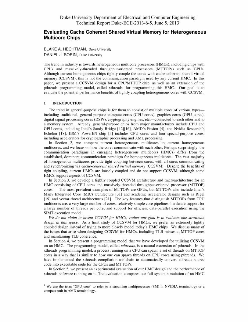
Figure 1. System Model. Network is actually a torus, but it is drawn as a mesh for clarity.
4
Our HMC’s CCSVM design is intentionally unoptimized and not tuned to the specific system
model. Where possible, we make conservative assumptions (e.g., our cache coherence protocol
does not treat MTTOP cores differently from CPU cores, despite their known behavioral
differences). Our goal is to isolate the impact of CCSVM without muddying the picture with
optimizations. If unoptimized CCSVM outshines existing designs, then the difference is due to
CCSVM itself and not due to any particular optimization.
3.1 Chip Organization
The chip consists of CPU cores and MTTOP cores that are connected together via some
interconnection network. Each CPU core and each MTTOP core has its own private cache (or
cache hierarchy) and its own private TLB and page table walker. All cores share one or more
levels of globally shared cache. This cache is logically shared and CPU and MTTOP cores can
communicate via loads and stores to this cache. This shared cache is significantly different than
the physically shared but logically partitioned last-level cache in Intel’s SandyBridge and
IvyBridge chips; in the Intel chips, communication between CPU and GPU cores must still occur
via off-chip DRAM.4 We do not differentially manage the cache for fairness or performance
depending on the core initiating the request [24].
We illustrate the organization of our specific microarchitecture in Figure 1, in which the CPU
and MTTOP cores communicate over a 2D torus interconnection network (drawn as a mesh, rather
than torus, for clarity). In this design, the shared L2 cache is banked and co-located with a banked
directory that holds state used for cache coherence.
One detail not shown in the figure is our introduction of a simple controller called the MTTOP
InterFace Device (MIFD). The MIFD’s purpose is to abstract away the details of the MTTOP
(including how many MTTOP cores are on the chip) by providing a general interface to the
collection of MTTOP cores. The MIFD is similar to the microcontrollers used to schedule tasks on
current MTTOPs. When a CPU core launches a task (a set of threads) on the MTTOP, it
communicates this task to the MIFD via a write syscall, and the MIFD finds a set of available
MTTOP thread contexts that can run the assigned task. Task assignment is done in a simple round-
robin manner until there are no MTTOP thread contexts remaining. The MIFD does not guarantee
that a task that requires global synchronization will be entirely scheduled, but it will write an error
register if there are not enough MTTOP thread contexts available. The MIFD thus enables an
architecture in which the number of MTTOP cores is a microarchitectural feature. The MIFD
driver is a very simple piece of code (~30 lines), unlike drivers for current MTTOPs that perform
JIT compilation from the HLL to the MTTOP’s native machine language. The primary purposes
of this driver are to assign threads to MTTOP cores, arbitrate between CPU processes seeking to
launch MTTOP threads, and set up the virtual address space on the MTTOP cores.
3.2 Cache-Coherent Shared Virtual Memory
The key aspect of our architecture is to extend CCSVM from homogeneous to heterogeneous
chips.
3.2.1 Shared Virtual Memory (SVM)
Architecture. In all SVM architectures (for homogeneous or heterogeneous chips), all threads
from a given process share the same virtual address space, and they communicate via loads and
stores to this address space. The system translates virtual addresses to physical addresses, with the
common case being that a load/store hits in the core’s TLB and quickly finds the translation it
needs. We assume that the caches are physically addressed (or at least physically tagged), as in all
current commercial chips of which we are aware.
There are several possible differences between SVM architectures. For one, how are TLB
misses handled? Some architectures specify that TLB misses are handled by trapping into the OS,
whereas others specify that a hardware page table walker will handle the miss. Second, there is
often architectural support for managing the page table itself, such as x86’s CR3 register that is an
architecturally-visible register that points to the root of the process’s page table. Third, there is a
4 http://www.anandtech.com/print/3922
http://www.realworldtech.com/page.cfm?ArticleID=RWT080811195102&p=9
5
range of architectural support for maintaining TLB coherence. Some architectures provide special
instructions or interrupts to accelerate the process of TLB shootdown [38]. Because the CPU
cores in the target system we study are x86, our HMC faithfully adheres to x86-specific
architectural decisions, including the use of a hardware TLB miss handler (page table walker).
Microarchitecture. Satisfying the x86 architecture, as it pertains to SVM, introduces some
interesting issues in our heterogeneous chip. Adding TLBs and page table walkers to each
MTTOP core is straightforward; we discuss the costs of adding them in Section 3.4. Sending the
contents of the CR3 register to a MTTOP core when a task begins (as part of the task descriptor
that is communicated via the write syscall to the MIFD) is also straightforward, although it does
require us to add a CR3 register to each MTTOP core. However, two other issues are more
complicated.
First, what happens when a MTTOP core encounters a page fault? The MTTOP core misses in
its TLB and its page table walker identifies the miss as a page fault. On a CPU core, a page fault
traps to the OS, but today’s MTTOP cores are not (yet) running the OS. A relatively simple
solution to this problem is to have the MTTOP core interrupt a CPU core, with the interrupt
signaling that the CPU core should handle the page fault. We implement this mechanism via the
MIFD, thus maintaining the abstraction that CPU cores do not need to be aware of specific
MTTOP cores or of the number of MTTOP cores. The MIFD, as a device, may interrupt a CPU
core on behalf of one of the MTTOP cores. One challenge, previously identified by IBM’s
PowerEN [12] and Intel’s research prototypes [40][41], is that, unlike when a CPU core page
faults, the interrupt occurs on the CPU core when the CPU core is not necessarily running the
process that page faulted. The PowerEN skirts this problem by requiring the software to
implement a user-level page fault handler on the CPU core. For CCSVM, we have the MTTOP
core interrupt the CPU core with the interrupt cause (page fault) and the x86 CR3 register that is
required to identify the necessary page table. AMD’s IOMMU design [1] takes a somewhat
similar approach of offloading GPU page faults to the CPU, but the request and acknowledgment
are performed over PCIe.
Second, how do we keep the TLBs at the MTTOP cores coherent? TLB coherence in all-CPU
chips is usually maintained via TLB shootdowns. A CPU core that modifies a translation sends an
interrupt to other cores that may be caching that translation in their TLBs, and those TLBs
invalidate their copies of the translation. On our chip, we must consider what happens when a
CPU core initiates a shootdown. (A MTTOP core may not trigger a shootdown, since it does not
run the OS and cannot modify translations.) We extend shootdown by having the CPU core signal
the TLBs at all MTTOP cores to flush. Flushing is conservative, in that we could have only
selectively invalidated entries, but it is a simple, viable option. A future consideration is to
incorporate the TLBs into the coherence protocol [30].
3.2.2 Cache Coherence
Architecture. Cache coherence is not, strictly speaking, an architectural issue. To be precise,
an architecture specifies only the memory consistency model (Section 3.2.3). However, virtually
all homogeneous systems with SVM provide hardware cache coherence as a key element in
supporting the consistency model.5 Cache coherence protocols ensure that cores cannot continue
to read stale values from their caches; protocols commonly enforce the “single writer or multiple
readers” (SWMR) invariant [35].
Microarchitecture. Because coherence protocols are not architecturally visible, we can choose
any protocol that is sufficient to support the desired consistency model. For our purposes, any
protocol that maintains the SWMR invariant suffices. In our implementation, we choose a
standard, unoptimized MOESI [37] directory protocol in which the directory state is embedded in
the L2 blocks, similar to recent Intel and AMD chips [34][6]. With an inclusive L2 cache (as in
Nehalem [34]), an L2 miss indicates that the block is not cached in any L1 and thus triggers an
access to off-chip memory. Our choice of protocol is noteworthy only insofar as the protocol
itself is not special. The assumption of write-back caches with coherence is a significant deviation
from current MTTOP cores that generally have write-through caches with the ability to bypass the
L1 for coherent reads, writes, and atomic operations. However, some current MTTOPs, such as
5 We do not consider software coherence [25] in this paper.
6
MIC and ARM’s Mali GPU [36], already provide cache-coherent shared memory or shared
memory without cache coherence, like AMD’s Heterogeneous System Architecture [39]. Recent
academic research has also explored cache coherence tailored specifically for GPUs (without
associated CPUs) [33]. We believe there is potential—in terms of performance and power—in
tailoring a coherence protocol for a specific HMC, to take advantage of its distinctive features; we
leave this research to future work.
3.2.3 Memory Consistency Model
Homogeneous chips with CCSVM support a memory consistency model [35]. The consistency
model specifies, at the architectural level, the legal orderings of loads and stores performed by
threads in a process. For example, sequential consistency (SC) [22] specifies that all loads and
stores must appear to perform in a total order, such that the total order respects the program order
at each thread and each load obtains the value of the most recent store (in the total order) to the
same address.
To the best of our knowledge, no heterogeneous chip has specified a clear memory consistency
model (presumably because they do not support CCSVM), although high-level languages (HLLs)
like CUDA and OpenCL provide ordering guarantees when programmers insert memory barrier
operations (e.g., CUDA’s thread fence and OpenCL’s read and write fences). Now that we are
considering CCSVM for heterogeneous chips, we believe it is time to specify an architectural-
level consistency model for these chips. An architectural consistency model would help
microarchitects to design systems by providing them with a clear specification of correctness. An
architectural consistency model would also help programmers, either those who write in xthreads
or those who write the software that supports HLLs.
The space of possible consistency models for arbitrary heterogeneous chips is enormous,
because of the rich variety of memory access instructions and memory access patterns. We leave
an exploration of this space for future work and instead, for now, conservatively provide a
sequentially consistent (SC) model.6 SC is the simplest model to reason about, and for the proof-
of-concept design in this paper we are willing to forego many optimizations that violate SC (e.g.,
we have no write buffers between the cores and their caches). SC is far more restrictive than the
memory models provided by current MTTOPs, particularly GPUs, which tend to prefer relaxed
models for graphics computations. Recent work explores consistency models for homogeneous
MTTOPs [15], but it is not clear how those results apply to HMCs that include MTTOPs. We are
not arguing for SC, and we believe more relaxed models are likely preferable in the future, but we
are advocating for the specification of precise consistency models.
3.2.4 Synchronization
Architecture: Our CCSVM architecture provides several synchronization primitives that can be
used to construct typical HLL synchronization constructs (e.g., locks, barriers, signal/wait). In
addition to the synchronization operations supported by the x86 CPU cores, the MTTOP ISA
provides simple atomic operations like those in OpenCL (e.g., atomic_cas, atomic_add,
atomic_inc, atomic_dec).
Microarchitecture: Today’s MTTOP cores tend to perform atomic instructions at the last-level
cache/memory rather than at the L1 cache as is often the case for CPUs. Because our goal is to
supportt general-purpose MTTOP code, rather than just graphics code, and because we want the
MTTOP cores to mesh well with the CPU cores, our MTTOP performs atomic operations at the
L1 after requesting exclusive coherence access to the block.
3.3 CCSVM’s Potential Benefits
The primary benefit of CCSVM is communication performance. As we show experimentally
in Section 5, CCSVM can vastly outperform hardware that requires the CPUs and MTTOPs to
communicate via off-chip DRAM. This result is intuitive; on-chip communication has far lower
6 Our x86 CPUs must satisfy the x86 consistency model [29]. Because the x86 model is more relaxed than
SC, SC is a valid implementation of the x86 model.

7
latency and far greater bandwidth. CCSVM provides a safe (coherent) mechanism for
transforming the vast majority of communication to be on-chip rather than off-chip.
CCSVM’s shift to on-chip communication has secondary potential benefits, including lower
energy and power costs (on-chip communication is more power- and energy- efficient than off-
chip) and greater effective off-chip memory bandwidth (because this bandwidth is not being used
for communication than can now be done on-chip).
The CCSVM architecture also offers two qualitative benefits. First, it has the virtue of being
similar to the CCSVM architectures that industry and academia are both already familiar with. All
other things being equal, familiarity is good. The community has a long history of designing,
validating, and programming (homogeneous) CCSVM machines, and this accumulated experience
and wisdom is a benefit when working on a new system. Second, CCSVM is an architecture with
a clean, clear specification. Being able to incorporate all cores, regardless of type, in the
architectural memory consistency model facilitates memory system design and validation, as well
as programming.
3.4 CCSVM’s Costs
Our CCSVM architecture and the specific microarchitecture we implement have their costs,
with respect to today’s HMCs. First, we have added page table walkers to each MTTOP. These
are small structures, compared to the size of a MTTOP, but they are not free. Nvidia and AMD
GPUs already have or soon will have TLBs [9], so we do not consider those an added cost for
CCSVM. Second, we have added the MIFD, which is a single small structure—similar to the
microcontroller in today’s GPUs—for the entire chip. Third, we have extended the on-chip
interconnection network to accommodate the MTTOPs. For the 2D torus in our microarchitecture,
this extension is simply a matter of adding nodes in the torus to which we attach the MTTOPs; we
do not need to increase the bandwidth of any switches or links to accommodate the MTTOPs.
Fourth, we have added a few bits per cache block for coherence state. Each of these four hardware
additions has area costs and energy/power costs, but none seem prohibitive. Without laying out an
entire chip, though, we cannot quantify these costs. One can also argue that the hardware and
power dedicated to CCSVM’s additional structures represents an opportunity cost, because this
hardware and power could be used for other purposes. Once again, we do not believe this
opportunity cost is great; even if it costs us the same as one MTTOP core (which is significantly
more than we expect), this is likely a reasonable tradeoff given the vast performance and power
benefits CCSVM achieves.
One potential qualitative cost of CCSVM is its complexity. CCSVM is indeed a more
complicated design than keeping the cores loosely coupled and having them communicate via
DMA. Fortunately, the community has a long history of producing (homogeneous) CCSVM
chips, and we believe industry can extend from homogeneous to heterogeneous chips.
Another potential drawback of CCSVM is a concern about coherence’s scalability. Some
architects believe that cache coherence does not scale to large numbers of cores, in which case
proposing it as an option for future heterogeneous chips would indeed be problematic. However,
based on recent analyses [10][28], we believe coherence will scale well enough for at least
hundreds of cores and likely more.
3.5 Compatibility with Graphics and with CUDA/OpenCL
The primary use of many MTTOPs—specifically, GPUs—is still graphics and we expect it to
remain this way for the foreseeable future. Thus we cannot allow our design, which is tailored for
general-purpose computation, to hinder the graphics capability of a chip. There is also an
established code base in CUDA and OpenCL that we cannot ignore. Fortunately our CCSVM
design is compatible with graphics and other legacy code. Legacy code can run using the existing
drivers and bypass our simple CCSVM driver. The caches can be reconfigured for use as
scratchpads [27], and we can disable the cache coherence hardware and page table walkers at the
MTTOPs. The interconnection network used for CCSVM is overkill for legacy code that has
little communication between MTTOPs, but it poses no problem for running legacy code.
8
4 Xthreads Programming Model
Given that we now have a CCSVM design for an HMC, we need to be able to write software
that takes advantage of having CCSVM. We developed xthreads with the goal of providing a
pthreads-like programming model that exploits CCSVM and is easy to use. We could not simply
adopt the current versions of OpenCL and CUDA, because they do not exploit CCSVM; however,
OpenCL or CUDA could be implemented to run on top of xthreads.
We do not claim that xthreads is optimal in any sense, nor do we wish to quantitatively
compare it to other programming models for heterogeneous chips. Rather, we have developed
xthreads as a proof-of-concept—that is, there exists at least one reasonable programming model
that enables us to demonstrate the benefits of CCSVM. Future work will delve more deeply into
improving and evaluating the programming model.
4.1 API
The xthreads API, summarized in Table 1, extends pthreads by enabling a thread on a CPU
core to spawn threads on non-CPU cores. For our system model in which the non-CPU cores are
MTTOP cores, the API’s create_mthread (“m” is for “MTTOP”) function enables a CPU thread
to spawn a set of SIMT threads that will run on one or more MTTOP cores (depending on the
microarchitecture). This function is roughly equivalent to (a) calling OpenCL’s
clEnEnqueueNDRange() with a work group size equal to the number of threads or (b) invoking a
CUDA kernel with one thread block. Given that CCSVM provides coherence across all threads
and all memory, there is no use having xthreads provide more levels of task splitting. Unlike
CUDA and OpenCL, xthreads does not require that a subset of threads needs to be located on the
same MTTOP core in order to enable communication between threads. Thus even small tasks can
be split up to use the entire MTTOP instead of one MTTOP core.
Table 1. Synopsis of Basic API Functions
Called
By
Function Description
CPU
create_mthread(void* fn, args* fnArgs, ThreadID firstThread, ThreadID lastThread)
Spawns a set of one or more MTTOP
threads that each runs the specified
function with the specified arguments.
wait(ConditionVar* condition, ThreadID firstThread, ThreadID lastThread, unsigned int waitCondition)
CPU thread sets array of condition
variables to WaitingOnMTTOP and
waits until MTTOP threads change
array elements to Ready. The
waitCondition argument could specify,
for example, that the CPU wait for
malloc requests from the MTTOP
threads.
signal(ConditionVar* condition, ThreadID firstThread, ThreadID lastThread)
CPU thread sets array of condition
variables to Ready so that MTTOP
threads can stop waiting
cpu_mttop_barrier(ThreadID firstThread, ThreadID lastThread, barrierArray* barrierArray, bool* sense)
CPU thread waits for all MTTOP
threads to write to array of barrier
locations, then CPU flips sense.
MTTOP
wait(ConditionVar* condition, ThreadID firstThread, ThreadID lastThread)
MTTOP threads set array of condition
variables to WaitingOnCPU and waits
until CPU changes these array elements
to Ready
signal(ConditionVar* condition, ThreadID firstThread, ThreadID lastThread)
MTTOP threads set array of condition
to Ready so that CPU thread can stop
waiting
cpu_mttop_barrier(barrierArray* barrierArray, bool* sense)
MTTOP thread writes to its barrier array
entry, then waits for sense to flip.
mttop_malloc(int size) Returns dynamically allocated memory
(like malloc)

9
The two primary mechanisms for synchronization are wait/signal and barrier. A CPU thread or
a set of MTTOP threads can wait until signaled by CPU or MTTOP threads. The wait/signal pair
operates on condition variables in memory. For example, a CPU thread can wait for an array of C
condition variables to all change from WaitingOnMTTOP to Ready, and this transition will occur
when C MTTOP threads have changed these condition variables to be Ready. The barrier
function is a global barrier across one CPU thread and a set of MTTOP threads. We considered
other types of barriers (e.g., a barrier that applies only to MTTOP threads) and a lock, but we
found that we did not need them for our algorithms.
4.2 Compilation Toolchain
We have implemented a compilation framework that enables us to easily convert xthreads
source code into an executable that runs on both the CPU and MTTOP cores. We illustrate the
compiler toolchain in Figure 2. This toolchain and the executable model (i.e., embedding the
MTTOP’s code in the text segment of the CPU’s executable) are quite similar to the CHI
prototype [40].
4.3 Runtime
When a process begins, the CPU cores begin executing threads as they would in a “normal”
pthreads application. The differences begin when a CPU thread calls create_mthread() for a
MTTOP task with N threads. For each task, the library performs a write syscall to the MTTOP
interface device. This write syscall describes a task as: {program counter of function, arguments
to function, first thread’s ID, CR3 register}. The MIFD then assigns incoming tasks to available
MTTOP cores. If a task specifies more threads than the SIMD width of a single MTTOP core,
then the task is distributed in SIMD-width chunks to multiple MTTOP cores. A SIMD-width
chunk is known as a warp in NVIDIA terminology and a wavefront in AMD terminology.
When a MTTOP core receives a task from the MIFD, it sets its CR3 register so that it can
participate in virtual address translation with the other threads (CPU and MTTOP) in the process.
The MTTOP core then begins executing from the program counter it receives. When it reaches an
Exit instruction, it halts and waits for the MIFD to send a new task.
4.4 Example of Xthreads vs. OpenCL
To illustrate the xthreads programming model and API, we provide a simple example. In
Figure 4 and Figure 3, we provide the xthreads and OpenCL code, respectively, for computing the
sum of two vectors of integers. The xthreads code is fairly simple and intuitive. There is a
minimum amount of overhead to create tasks and set up the MTTOP. The OpenCL code is far
more complicated, largely because of all of the work it has to do to explicitly communicate
between the CPU and the MTTOP. Increased code complexity obviously does not directly lead to
poorer performance, but it does reveal situations in which more work must be done.
Figure 2. Compilation Toolchain
10
In the kernel file __kernel void vector_add(__global __read_only int * v1,
__global __read_only int * v2, __global __write_only int * sum){
unsigned int tid = get_global_id(0); sum[tid] = v1[tid] + v2[tid]; }
In the host file int main(){ cl_platform_id platform_id = NULL; cl_device_id device_id = NULL; cl_uint ret_num_devices, ret_num_platforms; cl_int ret; ret = clGetPlatformIDs(1, &platform_id, &ret_num_platforms); ret = clGetDeviceIDs( platform_id,CL_DEVICE_TYPE_DEFAULT,1,&device_id, &ret_num_devices); // Create an OpenCL context cl_context context = clCreateContext( NULL, 1, &device_id, NULL, NULL, &ret); // Create a command queue cl_command_queue cmd_queue = clCreateCommandQueue(context, device_id, 0, &ret); cl_program program = clCreateProgramWithSource(context, 1, (const char **)&source_str, (const size_t *)&source_size, &ret); // Build the program
ret = clBuildProgram(program, 0/*1*/, 0/*&device_id*/, NULL, NULL, NULL); cl_mem v1_mem_obj = clCreateBuffer(context, CL_MEM_ALLOC_HOST_PTR | CL_MEM_READ_WRITE,256*sizeof(int), NULL, &ret); cl_mem v2_mem_obj = clCreateBuffer(context, CL_MEM_ALLOC_HOST_PTR | CL_MEM_READ_WRITE, 256*sizeof(int), NULL, &ret); cl_mem sum_mem_obj = clCreateBuffer(context, CL_MEM_ALLOC_HOST_PTR | CL_MEM_READ_WRITE, 256*sizeof(int), NULL, &ret); int *v1 = (int*)clEnqueueMapBuffer(cmd_queue, v1_mem_obj, CL_TRUE, 0, 0, 256*sizeof(int),0, NULL, NULL,NULL); int *v2 = (int*)clEnqueueMapBuffer(cmd_queue, v2_mem_obj, CL_TRUE, 0, 0, 256*sizeof(int),0, NULL, NULL,NULL); for(int i = 0; i < 256; i++) { v1[i] = rand(); v2[i] = rand(); } clEnqueueUnmapMemObject(cmd_queue,v1_mem_obj,a,0,NULL,NULL); clEnqueueUnmapMemObject(cmd_queue,v2_mem_obj,b,0,NULL,NULL); cl_kernel kernel = clCreateKernel(program, "vector_add", &ret); // Execute the OpenCL kernel on the list size_t global_item_size = size ; // Process the entire lists
size_t gsize = size ; // Process the entire list size_t local_item_size = (size<64)?size:64; // Process one item at a time
global_item_size = global_item_size/local_item_size; cl_event x; ret=clSetKernelArg(kernel, 0, sizeof(int), &size); ret = clSetKernelArg(kernel, 1, sizeof(cl_mem), (void *)&v1_mem_obj); ret = clSetKernelArg(kernel, 2, sizeof(cl_mem), (void *)&v2_mem_obj); ret = clSetKernelArg(kernel, 3, sizeof(cl_mem), (void *)&sum_mem_obj); ret = clEnqueueNDRangeKernel(cmd_queue, kernel, 1, NULL, &gsize, NULL, 0, NULL,NULL); clFinish(cmd_queue); clEnqueueUnmapMemObject(cmd_queue,sum_mem_obj,sum,0,NULL,NULL); clReleaseMemObject(v1_mem_obj); clReleaseMemObject(v2_mem_obj); clReleaseMemObject(sum_mem_obj); return 0; }
Figure 3. OpenCL Code

11
5 Experimental Evaluation
The goal of this evaluation is to quantitatively determine the viability of the CCSVM system
model for heterogeneous chips, for at least the specific implementation of it we have presented,
and the xthreads programming model. We believe this is the first experimental evaluation of the
impact of CCSVM on performance, memory access efficiency, and programmability. We also
believe that this is the first experimental evaluation of a CPU/MTTOP chip executing code with
pointer-based data structures. Throughout this evaluation, we focus on the memory system and
communication; we try to factor out the details of the CPU and MTTOP core pipelines, which are
orthogonal to this work.
5.1 Methodology and Target System
We have implemented our chip design in the gem5 full-system simulator [2]. Our extensions
to gem5 enable it to faithfully model the functionality and timing of the entire system. The
simulated CPU cores are in-order x86 cores that run unmodified Linux 2.6 with the addition of our
simple MIFD driver (~30 lines of C code). The MTTOP cores are SIMT cores that have an
Alpha-like ISA that has been modified to be data parallel. The MTTOP’s ISA is also similar to
PTX, the assembly-like intermediate language to which CUDA is compiled and that Nvidia
drivers convert to the native ISA of Nvidia GPUs. The details of the target system are in Table 2.
Evaluating the performance of CCSVM running xthreads benchmarks is somewhat challenging
for two reasons. First, no xthreads benchmarks existed prior to this work, so we have had to port
and re-write benchmarks. Second, comparing the performance of CCSVM to other system models
is complicated by the different programming models and the complexity of modeling existing
systems. For example, to truly model Intel’s SandyBridge or an AMD Fusion chip in a
comparable way, we would need access to its driver and its native ISA, among other information
that is not publicly available. We fundamentally cannot simulate a currently available HMC and,
as academics, we cannot implement a complete HMC in hardware.
struct args{ int* v1, v2, sum; // 3 vectors of ints
bool* done; }
_MTTOP_ void add(int tid, args* arg){ arg->sum[tid]=arg->v1[tid] +arg->v2[tid]; mthread_signal(arg->done); }
_CPU_ int main(int argc, char** argv){ args inputs; inputs.v1=malloc(256*sizeof(int)); inputs.v2=malloc(256*sizeof(int)); inputs.sum=malloc(256*sizeof(int)); inputs.done=malloc(256*sizeof(bool)); for(int i=0;i<256;i++){ inputs.v1[i]=rand(); inputs.v2[i]=rand(); inputs.done[i]=0; } mthread_create(0,256,&add,&inputs); mthread_wait(0,255,inputs.done); free(inputs.v1); free(inputs.v2); free(inputs.sum); free(inputs.done); }
Figure 4. Xthreads Code

12
Thus, we cannot perform a perfectly equivalent “apples-to-apples” comparison. Instead, we
compare a real, current HMC to a simulator of our CCSVM design and configure the simulator to
be conservative so as to favor the current HMC over our design. We purchased an AMD “Llano”
system based on its Quad-Core A8-3850 APU [11], and we use this real hardware running
OpenCL software for comparisons to CCSVM running xthreads software. The APU’s
specifications are in Table 2.
The configuration parameters show how we favor the APU over the CCSVM design. Notably,
the simulated CCSVM CPU cores are in-order and capable of executing only one instruction every
other cycle (i.e., max IPC is 0.5); thus, the simulated CCSVM CPU cores perform far worse than
the CPU cores in the APU. Also, the maximum throughput of the simulated CCSVM MTTOP is
less than that of the APU’s GPU by a factor equal to the utilization of the VLIW width of the
APU’s GPU cores. When the APU’s GPU is fully utilizing each VLIW instruction, it has a
throughput that is 4x that of the simulated CCSVM’s MTTOP; when the APU’s GPU is at its
minimum VLIW utilization, its throughput is equal to that of the CCSVM MTTOP.
5.2 Performance on “Typical” General Purpose Benchmarks
We have argued that the loose coupling between the CPU and MTTOP cores in today’s
systems is inefficient. To experimentally demonstrate the potential benefits of tighter coupling
between the CPU and MTTOP cores, we first compare the execution of a (dense) matrix
multiplication kernel that is launched from a CPU to as many MTTOP cores as can be utilized for
the matrix size. Intuitively, the overhead to launch a task will be better amortized over larger task
sizes, and the benefit of CCSVM will be highlighted by how it enables smaller tasks to be
profitably offloaded to the MTTOP cores. In Figure 5, we plot the log-scale runtimes of the AMD
APU running OpenCL code and CCSVM running xthreads code, relative to the AMD CPU core
(i.e., just using the CPU core on the APU chip), as a function of the matrix sizes. For the APU, we
present two runtime datapoints: full runtime and runtime without compilation and without
OpenCL initialization code.
The results are striking: CCSVM/xthreads greatly outperforms the APU, especially for smaller
matrix sizes. Eventually, as the matrices reach 1024x1024, the APU’s performance catches up to
CCSVM/xthreads, because the APU’s raw GPU performance exceeds that of our simulated
Table 2. Simulated CCSVM System and AMD System Configurations
CCSVM System (simulated) AMD APU (A8-3850 hardware) [11]
CPU 4 in-order x86 cores, 2.9 GHz, max IPC=0.5 4 out-of-order x86 cores, 2.9GHz, max
IPC=4
MTTOP • 10 MTTOP cores with Alpha-like ISA,
600MHz.
• Combined max of 80 operations per cycle
• Each MTTOP core supports 128 threads and
can simultaneously execute 8 threads.
• 5 SIMD processing units with 16 VLIW
Radeon cores per SIMD unit, 600 MHz.
• Combined max of 80 VLIWinstrs/cycle
• Each VLIW instruction is 1-4 operations
(max 320 operations per cycle).
On-chip
memory • Each CPU core has:
L1I, L1D: write-back, 64KB, 4-way, 2-
cycle hit
TLB: 64-entry, fully-associative
• Each MTTOP core has:
L1I, L1D: write-back, 16KB, 4-way, 1-
cycle hit
TLB: 64-entry, fully-associative
• All CPU and MTTOP cores share an
inclusive 4MB L2:
4 1MB banks, 10 CPU cycles, 2 MTTOP
cycles
• Each CPU core has:
L1I, L1D: 64KB, 4-way, 1ns hit
L2: 1 MB, 3.6ns hit
L2 TLB: 1024-entry
• Each SIMD processing unit has:
32KB of local memory
Off-chip
memory
2GB DRAM, hit latency 100ns 8GB DDR3 DRAM, hit latency 72ns
On-chip
network
2D torus, 12 GB/s link bandwidth CPUs connected to each other via crossbar
CPUs and GPUs fully connected to
memory controllers

13
MTTOP cores. The results dramatically confirm that optimizing the communication between
the CPU and MTTOP cores offers opportunities for vastly greater performances and for profitably
offloading smaller units of work to MTTOP cores, thus increasing their benefits.
In Figure 6, we plot the log-scale runtime results for a different benchmark: all-pairs shortest
path. The algorithm is a triply-nested loop that fills out an adjacency matrix—each (x,y) entry of
the adjacency matrix is the distance between nodes x and y in a directed graph—with the shortest
path from each node to each other node. The algorithm requires a barrier between each iteration
of the outermost loop. Because the APU’s synchronization is quite slow, the APU’s performance
never exceeds that of simply using the CPU core. As with the matrix multiplication benchmark,
CCSVM/xthreads vastly outperforms the APU/OpenCL over a range of matrix sizes. Even after
factoring out the OpenCL compilation and initialization time, CCSVM outperforms the APU by
approximately two orders of magnitude.
5.3 Performance on “Atypical” General Purpose Benchmarks
We now explore two benchmarks that highlight the ability of CCSVM/xthreads to extend the
types of computations that can be performed on CPU/MTTOP chips.
Figure 5. Performance on Matrix Multiply. Results show how CCSVM reduces overhead to launch
MTTOP tasks.
Figure 6. Performance on All-Pairs Shortest Path. Results show how CCSVM improves
performance by avoiding multiple MTTOP task launches for each parallel phase.
14
5.3.1 Pointer-Based Data Structures, Recursion, and Frequent CPU-MTTOP Communication
We ported the well-known barnes-hut n-body simulation benchmark from a pthreads version.
This benchmark extensively uses pointers and recursion and, most problematically for current
CPU/MTTOP chips, involves frequent toggling between sequential and parallel phases. Ideally,
we would like to use the CPU core for the sequential phases and the MTTOP cores for the parallel
phases, but switching between them on current HMCs is too slow to be viable. However, with
CCSVM/xthreads, this switching between them and the associated CPU-MTTOP communication
is fast and efficient. In Figure 7, we show the runtime of CCSVM/xthreads compared to a single
AMD CPU core. We also compare to the pthreads version of the benchmark running with 4
threads on the 4 CPU cores on the AMD APU. We could not find or develop an OpenCL version
of this benchmark against which to compare, so we could not exploit the APU’s GPU. We are
aware that there are techniques to perform the n-body problem without pointer-chasing [5], but we
use the barnes-hut application as a “strawman” for parallelizable pointer-based applications. The
results show that CCSVM/xthreads can outperform pthreads even for small problem sizes. There
is great potential to use MTTOP cores to accelerate important algorithms, and this potential is
unlocked by an HMC with CCSVM running xthreads code that exploits it.
5.3.2 Pointer-Based, Dynamically Allocated Data Structures
CCSVM with xthreads enables programmers to use space-efficient, pointer-based, dynamically
allocated shared data structures. The only CPU-MTTOP software that partially provides this
capability is CUDA 4.0 (released May 2011), which provides dynamic allocation for a subset of
data types. Unless using CUDA 4.0, programmers convert data structures that would typically be
pointer-based and dynamically allocated into statically allocated array-based structures, often at a
huge expense in storage.
To support these types of benchmark, we added a mttop_malloc() function to the xthreads API.
The mttop_malloc() function offloads the malloc to a CPU by having the CPU wait for the
MTTOP threads to signal the CPU that they wish to dynamically allocate memory. When the
CPU receives these signals, it performs the malloc() functions on their behalf and returns pointers
to the MTTOP threads. This approach to dynamically allocating memory at the MTTOP is not
particularly efficient or elegant, but it does demonstrate that it is possible; future work will involve
optimizing this process.
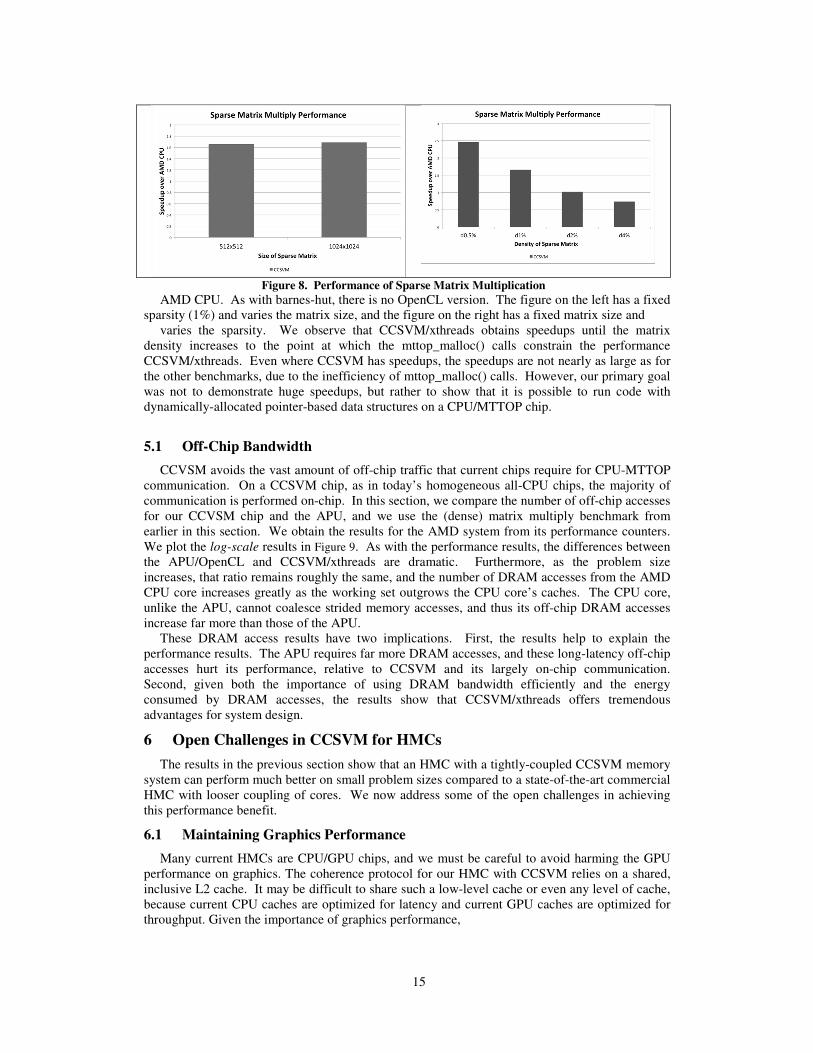
To demonstrate the viability of dynamic allocation on CCSVM/xthreads, we developed a
sparse matrix multiplication benchmark. For extremely large, sparse matrices, the only tractable
way to represent them is with pointer-based data structures that link non-zero elements. In Figure
8, we plot the speedup of CCSVM/xthreads on this benchmark, relative to the performance on the
Figure 7. Barnes-Hut performance. CCSVM/xthreads enables pointer chasing code.
15
AMD CPU. As with barnes-hut, there is no OpenCL version. The figure on the left has a fixed
sparsity (1%) and varies the matrix size, and the figure on the right has a fixed matrix size and
varies the sparsity. We observe that CCSVM/xthreads obtains speedups until the matrix
density increases to the point at which the mttop_malloc() calls constrain the performance
CCSVM/xthreads. Even where CCSVM has speedups, the speedups are not nearly as large as for
the other benchmarks, due to the inefficiency of mttop_malloc() calls. However, our primary goal
was not to demonstrate huge speedups, but rather to show that it is possible to run code with
dynamically-allocated pointer-based data structures on a CPU/MTTOP chip.
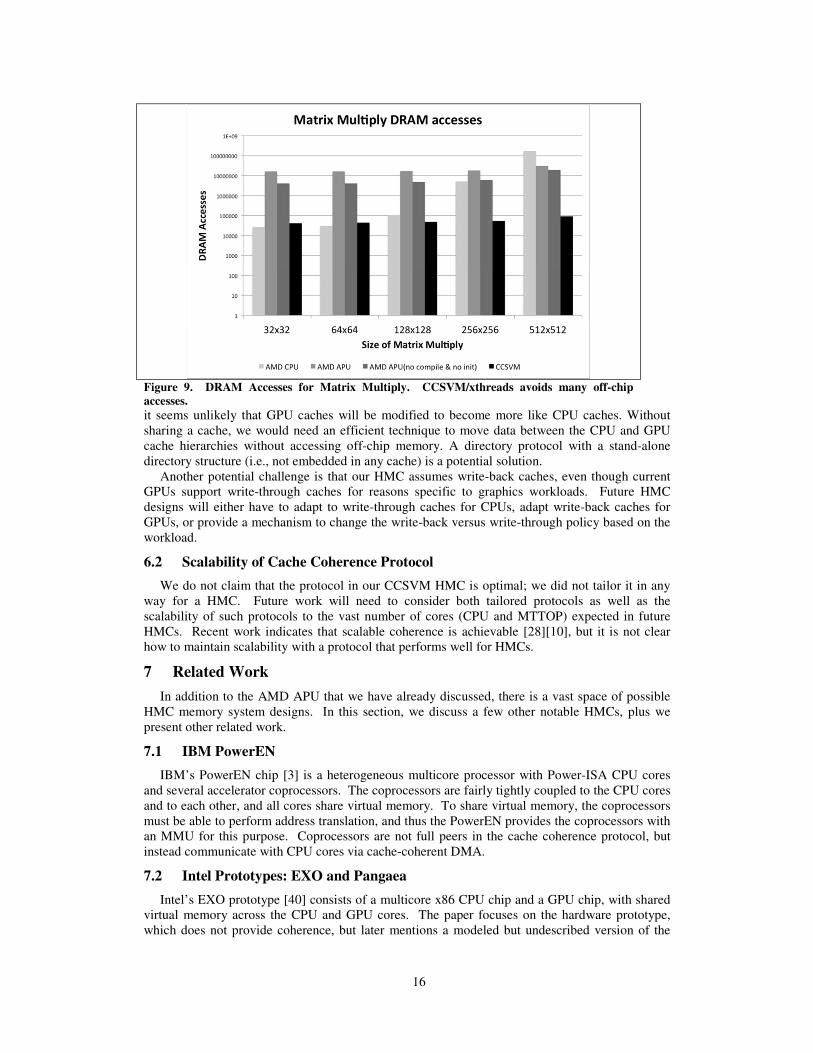
5.1 Off-Chip Bandwidth
CCVSM avoids the vast amount of off-chip traffic that current chips require for CPU-MTTOP
communication. On a CCSVM chip, as in today’s homogeneous all-CPU chips, the majority of
communication is performed on-chip. In this section, we compare the number of off-chip accesses
for our CCVSM chip and the APU, and we use the (dense) matrix multiply benchmark from
earlier in this section. We obtain the results for the AMD system from its performance counters.
We plot the log-scale results in Figure 9. As with the performance results, the differences between
the APU/OpenCL and CCSVM/xthreads are dramatic. Furthermore, as the problem size
increases, that ratio remains roughly the same, and the number of DRAM accesses from the AMD
CPU core increases greatly as the working set outgrows the CPU core’s caches. The CPU core,
unlike the APU, cannot coalesce strided memory accesses, and thus its off-chip DRAM accesses
increase far more than those of the APU.
These DRAM access results have two implications. First, the results help to explain the
performance results. The APU requires far more DRAM accesses, and these long-latency off-chip
accesses hurt its performance, relative to CCSVM and its largely on-chip communication.
Second, given both the importance of using DRAM bandwidth efficiently and the energy
consumed by DRAM accesses, the results show that CCSVM/xthreads offers tremendous
advantages for system design.
6 Open Challenges in CCSVM for HMCs
The results in the previous section show that an HMC with a tightly-coupled CCSVM memory
system can perform much better on small problem sizes compared to a state-of-the-art commercial
HMC with looser coupling of cores. We now address some of the open challenges in achieving
this performance benefit.
6.1 Maintaining Graphics Performance
Many current HMCs are CPU/GPU chips, and we must be careful to avoid harming the GPU
performance on graphics. The coherence protocol for our HMC with CCSVM relies on a shared,
inclusive L2 cache. It may be difficult to share such a low-level cache or even any level of cache,
because current CPU caches are optimized for latency and current GPU caches are optimized for
throughput. Given the importance of graphics performance,
Figure 8. Performance of Sparse Matrix Multiplication
16
it seems unlikely that GPU caches will be modified to become more like CPU caches. Without
sharing a cache, we would need an efficient technique to move data between the CPU and GPU
cache hierarchies without accessing off-chip memory. A directory protocol with a stand-alone
directory structure (i.e., not embedded in any cache) is a potential solution.
Another potential challenge is that our HMC assumes write-back caches, even though current
GPUs support write-through caches for reasons specific to graphics workloads. Future HMC
designs will either have to adapt to write-through caches for CPUs, adapt write-back caches for
GPUs, or provide a mechanism to change the write-back versus write-through policy based on the
workload.
6.2 Scalability of Cache Coherence Protocol
We do not claim that the protocol in our CCSVM HMC is optimal; we did not tailor it in any
way for a HMC. Future work will need to consider both tailored protocols as well as the
scalability of such protocols to the vast number of cores (CPU and MTTOP) expected in future
HMCs. Recent work indicates that scalable coherence is achievable [28][10], but it is not clear
how to maintain scalability with a protocol that performs well for HMCs.
7 Related Work
In addition to the AMD APU that we have already discussed, there is a vast space of possible
HMC memory system designs. In this section, we discuss a few other notable HMCs, plus we
present other related work.
7.1 IBM PowerEN
IBM’s PowerEN chip [3] is a heterogeneous multicore processor with Power-ISA CPU cores
and several accelerator coprocessors. The coprocessors are fairly tightly coupled to the CPU cores
and to each other, and all cores share virtual memory. To share virtual memory, the coprocessors
must be able to perform address translation, and thus the PowerEN provides the coprocessors with
an MMU for this purpose. Coprocessors are not full peers in the cache coherence protocol, but
instead communicate with CPU cores via cache-coherent DMA.
7.2 Intel Prototypes: EXO and Pangaea
Intel’s EXO prototype [40] consists of a multicore x86 CPU chip and a GPU chip, with shared
virtual memory across the CPU and GPU cores. The paper focuses on the hardware prototype,
which does not provide coherence, but later mentions a modeled but undescribed version of the
Figure 9. DRAM Accesses for Matrix Multiply. CCSVM/xthreads avoids many off-chip
accesses.

17
design that provides coherence. Unlike typical homogeneous systems with CCSVM, the GPU
cores do not have data caches.
Intel’s Pangaea prototype [41] is a chip with CPU and GPU cores that share a virtual address
space and share an L2 cache. As in EXO, the GPU cores do not have data caches, thus avoiding
many coherence issues. Coherence between the GPU and the CPU cores’ writeback L1 caches is
enforced only at the request of software. Software can specify that a region of shared virtual
memory is to be coherent, and only that region is kept coherent. Using software to manage
coherent regions of memory is a key difference between Pangaea and today’s CCVSM
homogeneous chips which use hardware coherence.
7.3 Evaluations of CPU/GPU Chips
Researchers have recently compared the performance of workloads running on CPU/GPU chips
and, in the process, have uncovered numerous performance issues. Gregg and Hazelwood [14]
experimentally showed that the time to transfer data between CPU and GPU cores must be
considered to avoid misleading conclusions; their results inspire work, such as ours, to reduce the
overhead of communication between CPU and GPU cores. Similarly, Daga et al. [8] showed that
the AMD APU’s performance is far better than previous designs in which the CPU and GPU cores
communicated over PCIe. Lee et al. [26] showed how certain performance evaluations have
unfairly favored GPUs, with respect to CPUs.
8 Conclusions
We have demonstrated that the tight coupling of cores provided by CCSVM can potentially
offer great benefits to an HMC. We do not claim that our CCVSM architecture, chip
microarchitecture, or xthreads programming model are “optimal,” assuming that optimality could
even be defined. Rather, our CCSVM architecture with the xthreads programming model is a
functional and promising starting point for future research into new features (e.g., programming
language extensions) and optimizations for performance and efficiency (e.g., coherence protocols
and consistency models tailored for heterogeneous chips, OS support for CCSVM on non-CPU
cores, etc.).
9 Acknowledgments
This material is based on work supported by AMD and by the National Science Foundation
under grant CCF-1216695.
10 References
[1] Advanced Micro Devices, Inc., AMD I/O Virtualization Technology (IOMMU) Specification.
Publication #48882, Revision 2.00, 2011.
[2] N. Binkert et al., “The Gem5 Simulator,” ACM SIGARCH Computer Architecture News, vol. 39, p. 1,
Aug. 2011.
[3] J. D. Brown, S. Woodward, B. M. Bass, and C. L. Johnson, “IBM Power Edge of Network Processor:
A Wire-Speed System on a Chip,” IEEE Micro, vol. 31, no. 2, pp. 76–85, Apr. 2011.
[4] B. Burgess, B. Cohen, M. Denman, J. Dundas, D. Kaplan, and J. Rupley, “Bobcat: AMD’s Low-
Power x86 Processor,” IEEE Micro, vol. 31, no. 2, pp. 16–25, Mar. 2011.
[5] M. Burtscher and K. Pingali, “An Efficient CUDA Implementation of the Tree-based Barnes Hut n-
Body Algorithm,” in GPU Computing Gems Emerald Edition, 2011, pp. 75–92.
[6] P. Conway and B. Hughes, “The AMD Opteron Northbridge Architecture,” IEEE Micro, vol. 27, no.
2, pp. 10–21, Apr. 2007.
[7] P. Conway, N. Kalyanasundharam, G. Donley, K. Lepak, and B. Hughes, “Cache Hierarchy and
Memory Subsystem of the AMD Opteron Processor,” IEEE Micro, vol. 30, no. 2, pp. 16–29, Apr.
2010.
[8] M. Daga, A. M. Aji, and W. Feng, “On the Efficacy of a Fused CPU+GPU Processor (or APU) for
Parallel Computing,” 2011, pp. 141–149.
[9] E. Demers, “Summit Keynote: Evolution of AMD’s Graphics Core, and Preview of Graphics Core
Next,” in AMD Fusion Developer Summit, 2011.
[10] M. Ferdman, P. Lotfi-Kamran, K. Balet, and B. Falsafi, “Cuckoo Directory: A Scalable Directory for
Many-Core Systems,” in IEEE 17th International Symposium on High Performance Computer
Architecture (HPCA), 2011, pp. 169–180.
18
[11] D. Foley et al., “AMD’s ‘Llano’ Fusion APU,” in Hot Chips 23, 2011.
[12] H. Franke et al., “Introduction to the Wire-Speed Processor and Architecture,” IBM J. Res. Dev., vol.
54, no. 1, pp. 27–37, Jan. 2010.
[13] I. Gelado, J. E. Stone, J. Cabezas, S. Patel, N. Navarro, and W. W. Hwu, “An Asymmetric Distributed
Shared Memory Model for Heterogeneous Parallel Systems,” in Proceedings of the International
Conference on Architectural Support for Programming Languages and Operating Systems, 2010, vol.
45, pp. 347–358.
[14] C. Gregg and K. Hazelwood, “Where is the data? Why you cannot debate CPU vs. GPU performance
without the answer,” in Proceedings of the IEEE International Symposium on Performance Analysis of
Systems and Software, 2011, pp. 134–144.
[15] B. A. Hechtman and D. J. Sorin, “Exploring Memory Consistency for Massively-Threaded
Throughput-Oriented Processors,” in Proceedings of the International Symposium on Computer
Architecture, 2013.
[16] Intel, “Intel® OpenSource HD Graphics Programmer’s Reference Manual (PRM), Volume 1, Part 1:
Graphics Core (SandyBridge).” May-2011.
[17] J. A. Kahle, M. N. Day, H. P. Hofstee, C. R. Johns, T. R. Maeurer, and D. Shippy, “Introduction to the
Cell Multiprocessor,” IBM Journal of Research and Development, vol. 49, no. 4.5, pp. 589–604, Jul.
2005.
[18] S. W. Keckler, W. J. Dally, B. Khailany, M. Garland, and D. Glasco, “GPUs and the Future of Parallel
Computing,” IEEE Micro, vol. 31, no. 5, pp. 7–17, Oct. 2011.
[19] J. H. Kelm et al., “Rigel: An Architecture and Scalable Programming Interface for a 1000-Core
Accelerator,” in Proceedings of the 36th Annual International Symposium on Computer Architecture,
2009, pp. 140–151.
[20] J. H. Kelm, D. R. Johnson, W. Tuohy, S. S. Lumetta, and S. J. Patel, “Cohesion: A Hybrid Memory
Model for Accelerators,” in Proceedings of the 37th Annual International Symposium on Computer
Architecture, 2010, pp. 429–440.
[21] R. Krashinsky et al., “The Vector-Thread Architecture,” in 31st International Symposium on
Computer Architecture, 2004, pp. 52–63.
[22] L. Lamport, “How to Make a Multiprocessor Computer that Correctly Executes Multiprocess
Programs,” IEEE Transactions on Computers, vol. C–28, no. 9, pp. 690–691, Sep. 1979.
[23] H. Q. Le and others, “IBM POWER6 Microarchitecture,” IBM Journal of Research and Development,
vol. 51, no. 6, 2007.
[24] J. Lee and H. Kim, “TAP: A TLP-Aware Cache Management Policy for a CPU-GPU Heterogeneous
Architecture,” in High Performance Computer Architecture (HPCA), 2012 IEEE 18th International
Symposium on, 2012, pp. 1 –12.
[25] J. Lee, J. Lee, S. Seo, J. Kim, S. Kim, and Z. Sura, “COMIC++: A Software SVM System for
Heterogeneous Multicore Accelerator Clusters,” in 2010 IEEE 16th International Symposium on High
Performance Computer Architecture (HPCA), 2010, pp. 1 –12.
[26] V. W. Lee et al., “Debunking the 100X GPU vs. CPU Myth: An Evaluation of Throughput Computing
on CPU and GPU,” in Proceedings of the 37th Annual International Symposium on Computer
Architecture, 2010, pp. 451–460.
[27] K. Mai, T. Paaske, N. Jayasena, R. Ho, W. Dally, and M. Horowitz, “Smart Memories: A Modular
Reconfigurable Architecture,” in Proceedings of the 27th Annual International Symposium on
Computer Architecture, 2000.
[28] M. M. K. Martin, M. D. Hill, and D. J. Sorin, “Why On-chip Cache Coherence is Here to Stay,”
Communications of the ACM, vol. 55, no. 7, pp. 78–89, Jul. 2012.
[29] S. Owens, S. Sarkar, and P. Sewell, “A Better x86 Memory Model: x86-TSO,” in Proceedings of the
Conference on Theorem Proving in Higher Order Logics, 2009.
[30] B. F. Romanescu, A. R. Lebeck, D. J. Sorin, and A. Bracy, “UNified Instruction/Translation/Data
(UNITD) Coherence: One Protocol to Rule Them All,” in Proceedings of the Fifteenth International
Symposium on High-Performance Computer Architecture, 2010.
[31] L. Seiler and et al., “Larrabee: A Many-Core x86 Architecture for Visual Computing,” in Proceedings
of ACM SIGGRAPH, 2008.
[32] M. Shah et al., “UltraSPARC T2: A Highly-Threaded, Power-Efficient, SPARC SOC,” in IEEE Asian
Solid-State Circuits Conferenec, 2007, pp. 22–25.
[33] I. Singh, A. Shriraram, W. W. L. Fung, M. O’Connor, and T. M. Aamodt, “Cache Coherence for GPU
Architectures,” in Proceedings of the 19th IEEE International Symposium on High-Performance
Computer Architecture, 2013, pp. 578–590.
[34] R. Singhal, “Inside Intel Next Generation Nehalem Microarchitecture,” in Hot Chips 20, 2008.
[35] D. J. Sorin, M. D. Hill, and D. A. Wood, A Primer on Memory Consistency and Cache Coherence,
Synthesis Lectures on Computer Architecture. Morgan & Claypool Publishers, 2011.
19
[36] S. Steele, “ARM GPUs: Now and in the Future.”
http://www.arm.com/files/event/8_Steve_Steele_ARM_GPUs_Now_and_in_the_Future.pdf, Jun-2011.
[37] P. Sweazey and A. J. Smith, “A Class of Compatible Cache Consistency Protocols and their Support
by the IEEE Futurebus,” in Proceedings of the 13th Annual International Symposium on Computer
Architecture, 1986, pp. 414–423.
[38] P. J. Teller, “Translation-Lookaside Buffer Consistency,” IEEE Computer, vol. 23, no. 6, pp. 26–36,
Jun. 1990.
[39] V. Tipparaju and L. Howes, “HSA for the Common Man.”
http://devgurus.amd.com/servlet/JiveServlet/download/1282191-1737/HC-4741_FINAL.pptx, 2012.
[40] P. H. Wang et al., “EXOCHI: Architecture and Programming Environment for a Heterogeneous Multi-
Core Multithreaded System,” in Proceedings of the 2007 ACM SIGPLAN conference on Programming
language design and implementation, 2007, pp. 156–166.
[41] H. Wong et al., “Pangaea: A Tightly-Coupled IA32 Heterogeneous Chip Multiprocessor,” in
Proceedings of the 17th international Conference on Parallel Architectures and Compilation
Techniques, 2008, pp. 52–61.
[42] M. Yuffe, E. Knoll, M. Mehalel, J. Shor, and T. Kurts, “A Fully Integrated Multi-CPU, GPU and
Memory Controller 32nm Processor,” in 2011 IEEE International Solid-State Circuits Conference,
2011, pp. 264–266.