Embed Size (px)
Citation preview
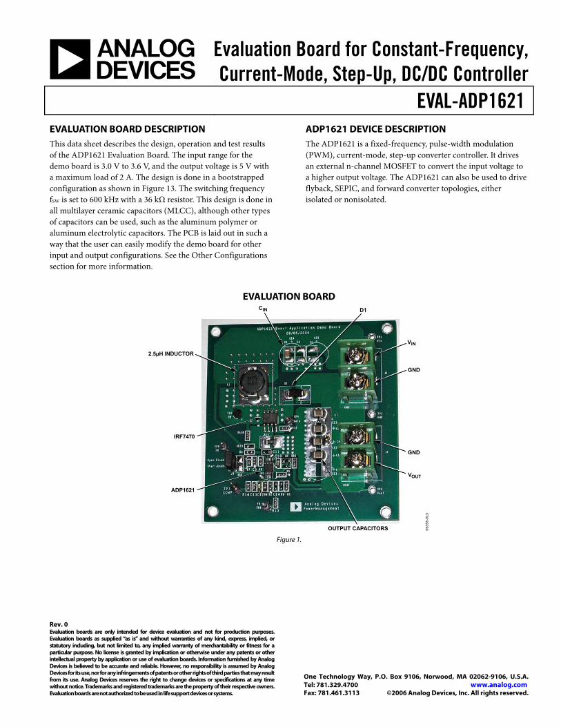
Evaluation Board for Constant-Frequency, Current-Mode, Step-Up, DC/DC Controller
EVAL-ADP1621
Rev. 0 Evaluation boards are only intended for device evaluation and not for production purposes. Evaluation boards as supplied “as is” and without warranties of any kind, express, implied, or statutory including, but not limited to, any implied warranty of merchantability or fitness for a particular purpose. No license is granted by implication or otherwise under any patents or other intellectual property by application or use of evaluation boards. Information furnished by Analog Devices is believed to be accurate and reliable. However, no responsibility is assumed by Analog Devices for its use, nor for any infringements of patents or other rights of third parties that may result from its use. Analog Devices reserves the right to change devices or specifications at any time without notice. Trademarks and registered trademarks are the property of their respective owners. Evaluation boards are not authorized to be used in life support devices or systems.
One Technology Way, P.O. Box 9106, Norwood, MA 02062-9106, U.S.A.Tel: 781.329.4700 www.analog.com Fax: 781.461.3113 ©2006 Analog Devices, Inc. All rights reserved.
EVALUATION BOARD DESCRIPTION This data sheet describes the design, operation and test results of the ADP1621 Evaluation Board. The input range for the demo board is 3.0 V to 3.6 V, and the output voltage is 5 V with a maximum load of 2 A. The design is done in a bootstrapped configuration as shown in Figure 13. The switching frequency fSW is set to 600 kHz with a 36 kΩ resistor. This design is done in all multilayer ceramic capacitors (MLCC), although other types of capacitors can be used, such as the aluminum polymer or aluminum electrolytic capacitors. The PCB is laid out in such a way that the user can easily modify the demo board for other input and output configurations. See the Other Configurations section for more information.
ADP1621 DEVICE DESCRIPTION The ADP1621 is a fixed-frequency, pulse-width modulation (PWM), current-mode, step-up converter controller. It drives an external n-channel MOSFET to convert the input voltage to a higher output voltage. The ADP1621 can also be used to drive flyback, SEPIC, and forward converter topologies, either isolated or nonisolated.
EVALUATION BOARD
VIN
GND
GND
VOUT
CIN
ADP1621
D1
2.5µH INDUCTOR
IRF7470
OUTPUT CAPACITORS 0635
8-01
3
Figure 1.
EVAL-ADP1621
Rev. 0 | Page 2 of 12
TABLE OF CONTENTS Evaluation Board Description......................................................... 1 ADP1621 Device Description......................................................... 1 Evaluation Board .............................................................................. 1 Revision History ............................................................................... 2 Evaluation Board Hardware ............................................................ 3
Component Selection................................................................... 3 Test Waveforms................................................................................. 6 PCB Layout Guideline ..................................................................... 8
Other Configurations ...................................................................8 Evaluation Board Schematic and Artwork.....................................9
PCB Layout ................................................................................. 10 Ordering Information.................................................................... 11
Bill of Materials........................................................................... 11 Ordering Guide .......................................................................... 11 ESD Caution................................................................................ 11
REVISION HISTORY 11/06—Revision 0: Initial Version
EVAL-ADP1621
Rev. 0 | Page 3 of 12
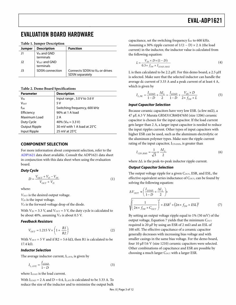
EVALUATION BOARD HARDWARE Table 1. Jumper Description Jumper Description Function J1 VIN and GND
terminals
J2 VOUT and GND terminals
J3 SDSN connection Connects SDSN to VIN or drives SDSN separately
Table 2. Demo Board Specifications Parameter Description VIN Input range , 3.0 V to 3.6 V VOUT 5 V fSW Switching frequency, 600 kHz Efficiency 90% at 1 A load Maximum Load 2 A Duty Cycle 40% (VIN = 3.3 V) Output Ripple 30 mV with 1 A load at 25°C Input Ripple 25 mV at 25°C
COMPONENT SELECTION For more information about component selection, refer to the ADP1621 data sheet available. Consult the ADP1621 data sheet in conjunction with this data sheet when using the evaluation board.
Duty Cycle
DOUT
INDOUT
VVVVV
D+−+
= (1)
where:
VOUT is the desired output voltage. VIN is the input voltage. VD is the forward-voltage drop of the diode.
With VIN = 3.3 V, and VOUT = 5 V, the duty cycle is calculated to be about 40%, assuming VD is about 0.5 V.
Feedback Resistors
⎟⎠⎞
⎜⎝⎛ +×=
R2R1VOUT 1V215.1 (2)
With VOUT = 5 V and if R2 = 5.6 kΩ, then R1 is calculated to be 17.4 kΩ.
Inductor Selection
The average inductor current, IL,AVE, is given by
DI
I LOADAVEL −
=1, (3)
where ILOAD is the load current.
With ILOAD = 2 A and D = 0.4, IL,AVE is calculated to be 3.33 A. To reduce the size of the inductor and to minimize the output bulk
capacitance, set the switching frequency fSW to 600 kHz. Assuming a 30% ripple current of 1/(1 − D) × 2 A (the load current) in the inductor, the inductor value is calculated from the following equation:
( )MAXLOADSW
IN
IfDDV
L,3.0
1××
−××= (4)
L is then calculated to be 2.2 μH. For this demo board, a 2.5 μH is selected. Make sure that the selected inductor can handle the average dc current of 3.33 A and a peak current of at least 4 A, which is given by
LfDV
DII
DI
ISW
INLOADLLOADPKL ××
×+
−=
Δ+
−=
2121, (5)
Input Capacitor Selection
Because ceramic capacitors have very low ESR. (a few mΩ), a 47 μF, 6.3 V Murata GRM31CR60J476M (size 1206) ceramic capacitor is chosen for the input capacitor. If the load current gets larger than 2 A, a larger input capacitor is needed to reduce the input ripples current. Other types of input capacitors with higher ESR can be used, such as the aluminum electrolytic or the aluminum polymer types. Make sure the ripple current rating of the input capacitor, ICIN,RMS, is greater than
231
,L
RMSCINI
IΔ
×= (6)
where ΔIL is the peak-to-peak inductor ripple current.
Output Capacitor Selection
The output voltage ripple for a given COUT, ESR, and ESL, the effective equivalent series inductance of COUT, can be found by solving the following equation:
×⎟⎠⎞
⎜⎝⎛ Δ
+−
≈Δ21
LLOADOUT
ID
IV
( )222
22
1 ESLfESRCf SW
OUTSW
××π++⎟⎟⎠
⎞⎜⎜⎝
⎛
××π (7)
By setting an output voltage ripple equal to 1% (50 mV) of the output voltage, Equation 7 yields that the minimum COUT required is 20 μF by using an ESR of 2 mΩ and an ESL of 100 nH. The effective capacitance of a ceramic capacitor generally decreases with increasing bias voltage and with smaller casings in the same bias voltage. For the demo board, four 10 μF/16 V (size 1210) ceramic capacitors were selected. Other combinations of capacitance and ESR are possible by choosing a much larger COUT with a larger ESR.
EVAL-ADP1621
Rev. 0 | Page 4 of 12
Diode Selection
The diode conducts the inductor current to the output capacitor and loads while the MOSFET is off. The average diode current is the load current,
LOADAVEDIODE II =, (8)
The rms diode current in continuous conduction mode is given by
DD
II LOAD
RMSDIODE −×−
= 11, (9)
where D is the duty cycle.
With a 2 A load, IDIODE,RMS is calculated to be 2.6 A. A Vishay SSA33L in a SMA package meets the dc current and thermal requirements.
MOSFET Selection
The power MOSFET must be chosen based on threshold voltage (VT), on resistance (RDSON), maximum voltage and current ratings, and gate charge. The RMS current through the MOSFET is given by the following equation:
DD
II LOAD
MOSFETRMS ×−
=1, (10)
where IRMS,MOSFET is calculated to be 2.1 A, assuming ILOAD is 2 A and D is 0.4.
The IRF7470 is a 40 V n-channel power MOSFET that meets the current and thermal requirements. It comes in an 8-lead SOIC package and offers low RDSON and gate charge. RDSON is 30 mΩ at VGS = 2.8 V and 15 mΩ at VGS = 4.5 V. This general-purpose MOSFET meets a wide range of output voltage and current requirements. An alternative to this part is the Vishay Si7883DP, a 20 V n-channel power MOSFET.
Loop Compensation
The location of the right hand plane (RHP) zero frequency is determined by the following equation:
( )L
RDf LOAD
RHPZ ×π×−=
21 2
, (11)
where:
fZ,RHP is the RHP zero frequency. RLOAD is the equivalent load resistance, or the output voltage divided by the load current.
To stabilize the regulator, ensure that the regulator crossover frequency is ≤1/5th of the RHP zero frequency and ≤1/15th of the switching frequency. With VOUT = 5 V at 2 A load, fZ,RHP is calculated to be 57.3 kHz.
For an initial practical design, set the crossover frequency fC to the lower frequency of
15SW
Cf
f = (12)
and
5,RHPZf
Cf = (13)
where:
fC is the crossover frequency. fSW is the switching frequency.
Equation 13 shows that fC is 40 kHz and is lower frequency than that of Equation 12. The loop compensation components are calculated to be RCOMP = 33 kΩ and CCOMP = 490 pF from Equation 14 and Equation 15, respectively. The final component values need to be tested and verified on the actual PCB.
RCOMP is given by
( ) mFB
OUTCSOUTCCOMP gDV
VRnCfR
×−××××××π
=1
2 (14)
where:
VFB = 1.215 V D = 0.4 gm = 300 μS RCS = 15 mΩ for the IRF7470 at VGS = 4.5 V VOUT = 5 V n = 9.5 (typically) COUT ≈ 40 μF fC = 40 kHz (fSW/15 = 60 kHz/15).
To fine-tune the RCOMP and CCOMP values on the evaluation board, run a step load, for example, from 0.2 A to 1 A, at the output and observe the output transient. If there is too much overshoot in the transient, increase RCOMP; if there is too much oscillation, increase CCOMP.
Once the compensation resistor RCOMP is known, set the zero formed by the resistor and compensation capacitor CCOMP to 1/4th of the crossover frequency, or
COMPCCOMP Rf
C××π
=2 (15)
A roll-off capacitor of C2 = 390 pF is also added on the demo board. A smaller C2 works fine.
Slope Compensation
The slope-compensation resistor RS = 142 Ω from the following equation:
( ) ( )LfI
ftVVVRR
SWPKSC
SWMINOFFINDOUTCSS ×××
×−×−+×>
,
,
21
(16)
where:
tOFF,MIN = 230 ns fSW = 600 kHz L = 2.5 μH ISC,PK = 70 μA.
EVAL-ADP1621
Rev. 0 | Page 5 of 12
Current Limit
The current limit in the ADP1621 limits the peak inductor current and is achieved by the COMP voltage clamp. The peak inductor current, IL,PK, is given by
CS
SWMINOFF
SPKSCZCTCOMPCLAMPCOMP
PKL RftDRI
nVV
I×−××
−−
= ,
,,,
,1
(17)
where:
VCOMP,CLAMP is the COMP clamp voltage (maximum 2.1 V). VCOMP,ZCT is the COMP zero-current threshold (typically 1.0 V). n is the current-sense amplifier gain (typically 9.5). ISC,PK is the peak slope-compensation current (typically 70 μA). RS is the slope-compensation resistor. D is the duty cycle. fSW is the switching frequency. tOFF,MIN is the minimum off time (typically 190 ns). RCS is the current-sense resistor.
The peak inductor current limit also limits the maximum load current at a given output voltage. The maximum load current, assuming continuous conduction mode (CCM) operation, is given by
( )×−= DI MAXLOAD 1,
⎟⎟⎟⎟⎟
⎠
⎞
⎜⎜⎜⎜⎜
⎝
⎛
×××
−×−××
−−
LfDV
RftDRI
nVV
SW
IN
CS
SWMINOFF
SPKSCZCTCOMPCLAMPCOMP
21 ,
,,,
(18)
where:
n = 9.5 VCOM,CLAMP = 2.1 V VCOMP,ZCT = 1.0 V.
The current limit, ILOAD,MAX, is calculated to be ~4 A for this demo board. Note that the diode SSA33L is not rated for continuous current operation at 4 A. The maximum load current for this demo board is designed for 2 A.
Note that the current limit in the ADP1621 is a soft current limit. When the inductor current reaches the IL,PK limit given in Equation 17, the duty cycle decreases, and the output voltage drops below the desired voltage. The IL,PK limit then increases in response to the smaller duty cycle, D. The larger the slope-compensation resistor (RS), the larger the effect on IL,PK for an incremental decrease in D. This behavior results in a soft current limit for the ADP1621. Use values of RS that are as close as possible to the calculated limit derived from Equation 16 to minimize the softness of the current limit while maintaining current-loop stability. If high-precision current limiting is required, consider inserting a fuse in series with the inductor.
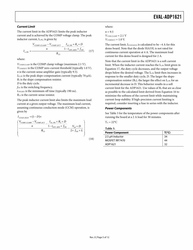
Power Components
See Table 3 for the temperature of the power components after running the board at a 2 A load for 30 minutes.
TA = 22°C
Table 3. Power Component T(°C) 2.5 μH Inductor 34 MOSFET IRF7470 44 ADP1621 32
EVAL-ADP1621
Rev. 0 | Page 6 of 12
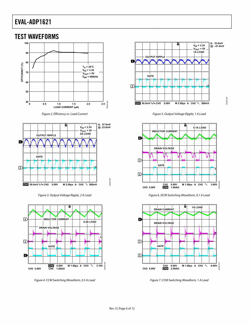
TEST WAVEFORMS
40
50
60
70
80
90
100
EFFI
CIE
NC
Y (%
)
LOAD CURRENT (µA)0 0.5 1.0 1.5 2.0 2.5
TA = 25°CVIN = 3.3VVOUT = 5VfSW = 600kHz
0635
8-00
2
Figure 2. Efficiency vs. Load Current
0635
8-00
3
CH1 50.0mV CH2 5.00V M 2.00µs A CH2 500mVBW
Δ: 57.0mV@: 23.0mV
2
1
VIN = 3.3VVOUT = 5V2A LOADOUTPUT RIPPLE
GATE
T
Figure 3. Output Voltage Ripple, 2 A Load
0635
8-00
4
4
2
CH3 5.00V CH4 1.00AΩ
3
0.5A LOAD
CH2 5.00V M 1.00µs A CH3 3.10V
GATE
DRAIN VOLTAGE
INDUCTOR CURRENT
T
Figure 4. CCM Switching Waveform, 0.5 A Load
0635
8-00
5
CH1 50.0mV CH2 5.00V M 2.00µs A CH2 500mVBW
2
1
Δ: 33.0mV@: –21.0mVVIN = 3.3V
VOUT = 5V1A LOAD
T
OUTPUT RIPPLE
GATE
Figure 5. Output Voltage Ripple, 1 A Load
0635
8-00
6
CH2 5.00V M 1.00µs A CH2 3.60V
2
4
CH3 5.00V CH4 1.00AΩ
3
DRAIN VOLTAGE
GATE
INDUCTOR CURRENT0.1A LOAD
T
Figure 6. DCM Switching Waveform, 0.1 A Load
0635
8-00
7
CH2 5.00V M 1.00µs A CH3 6.00V
2
4
T
CH3 5.00V CH4 2.00AΩ
3
DRAIN VOLTAGE
GATE
DRAIN CURRENT1A LOAD
Figure 7. CCM Switching Waveform, 1 A Load
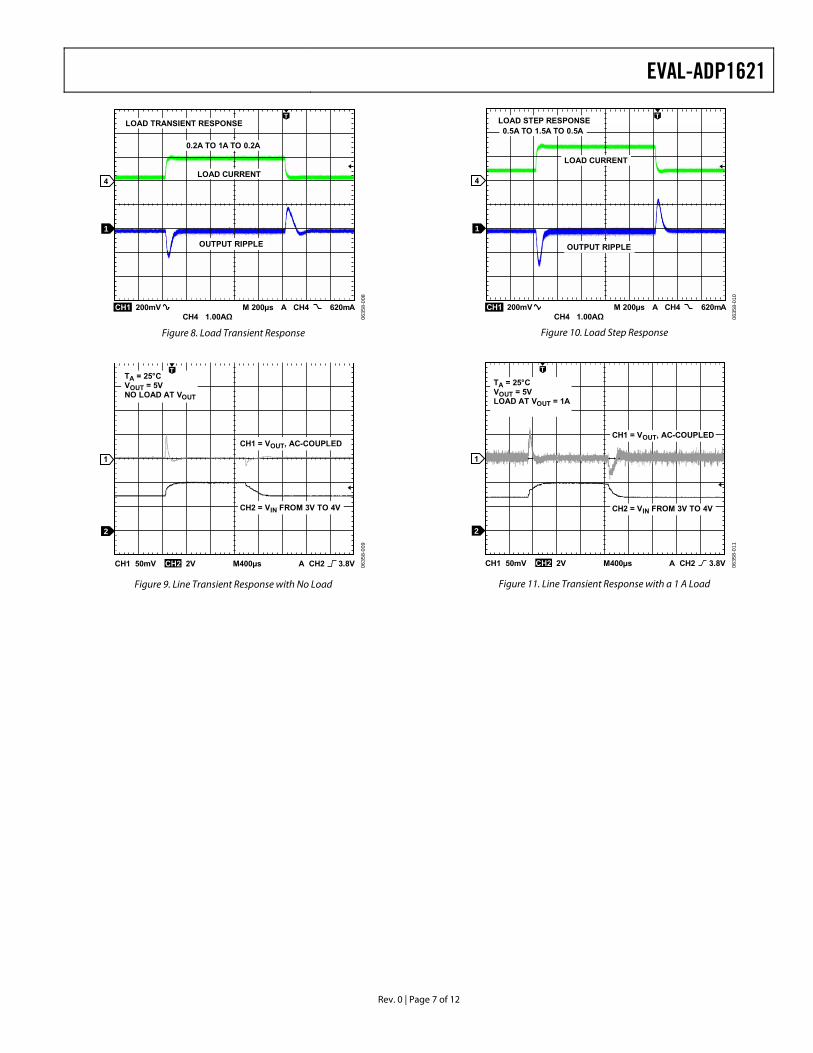
EVAL-ADP1621
Rev. 0 | Page 7 of 12
0635
8-01
0
CH1 200mV M 200µs A CH4 620mA CH4 1.00AΩ
4
1
T
LOAD CURRENT
OUTPUT RIPPLE
LOAD STEP RESPONSE0.5A TO 1.5A TO 0.5A
0635
8-00
8
CH1 200mV M 200µs A CH4 620mA CH4 1.00AΩ
4
1
T
LOAD CURRENT
OUTPUT RIPPLE
LOAD TRANSIENT RESPONSE
0.2A TO 1A TO 0.2A
Figure 10. Load Step Response Figure 8. Load Transient Response
CH1 50mV CH2 2V M400µs A CH2 3.8V
TA = 25°CVOUT = 5VLOAD AT VOUT = 1A
CH1 = VOUT, AC-COUPLED
CH2 = VIN FROM 3V TO 4V
0635
8-01
1
1
2
T
CH1 50mV CH2 2V M400µs A CH2 3.8V
TA = 25°CVOUT = 5VNO LOAD AT VOUT
CH1 = VOUT, AC-COUPLED
CH2 = VIN FROM 3V TO 4V
0635
8-00
9
1
2
T
Figure 11. Line Transient Response with a 1 A Load Figure 9. Line Transient Response with No Load
EVAL-ADP1621
Rev. 0 | Page 8 of 12
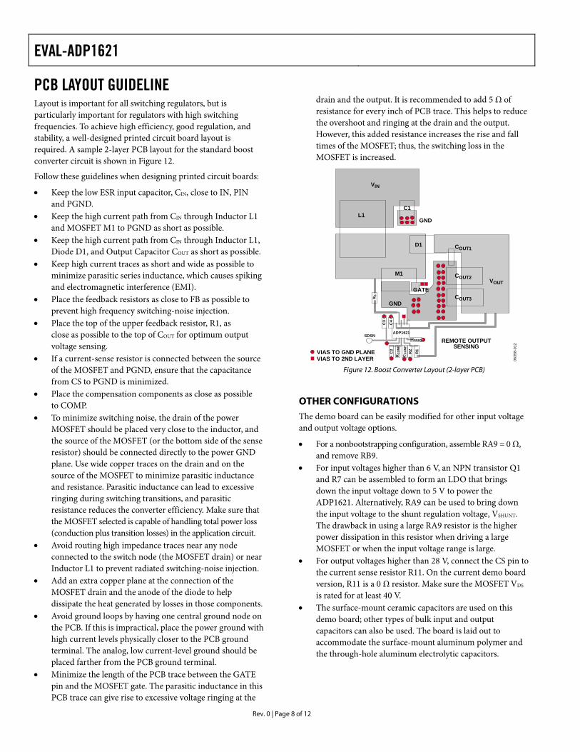
PCB LAYOUT GUIDELINELayout is important for all switching regulators, but is particularly important for regulators with high switching frequencies. To achieve high efficiency, good regulation, and stability, a well-designed printed circuit board layout is required. A sample 2-layer PCB layout for the standard boost converter circuit is shown in Figure 12.
Follow these guidelines when designing printed circuit boards:
• Keep the low ESR input capacitor, CIN, close to IN, PIN and PGND.
• Keep the high current path from CIN through Inductor L1 and MOSFET M1 to PGND as short as possible.
• Keep the high current path from CIN through Inductor L1, Diode D1, and Output Capacitor COUT as short as possible.
• Keep high current traces as short and wide as possible to minimize parasitic series inductance, which causes spiking and electromagnetic interference (EMI).
• Place the feedback resistors as close to FB as possible to prevent high frequency switching-noise injection.
• Place the top of the upper feedback resistor, R1, as close as possible to the top of COUT for optimum output voltage sensing.
• If a current-sense resistor is connected between the source of the MOSFET and PGND, ensure that the capacitance from CS to PGND is minimized.
• Place the compensation components as close as possible to COMP.
• To minimize switching noise, the drain of the power MOSFET should be placed very close to the inductor, and the source of the MOSFET (or the bottom side of the sense resistor) should be connected directly to the power GND plane. Use wide copper traces on the drain and on the source of the MOSFET to minimize parasitic inductance and resistance. Parasitic inductance can lead to excessive ringing during switching transitions, and parasitic resistance reduces the converter efficiency. Make sure that the MOSFET selected is capable of handling total power loss (conduction plus transition losses) in the application circuit.
• Avoid routing high impedance traces near any node connected to the switch node (the MOSFET drain) or near Inductor L1 to prevent radiated switching-noise injection.
• Add an extra copper plane at the connection of the MOSFET drain and the anode of the diode to help dissipate the heat generated by losses in those components.
• Avoid ground loops by having one central ground node on the PCB. If this is impractical, place the power ground with high current levels physically closer to the PCB ground terminal. The analog, low current-level ground should be placed farther from the PCB ground terminal.
• Minimize the length of the PCB trace between the GATE pin and the MOSFET gate. The parasitic inductance in this PCB trace can give rise to excessive voltage ringing at the
drain and the output. It is recommended to add 5 Ω of resistance for every inch of PCB trace. This helps to reduce the overshoot and ringing at the drain and the output. However, this added resistance increases the rise and fall times of the MOSFET; thus, the switching loss in the MOSFET is increased.
VIN
VIAS TO GND PLANEVIAS TO 2ND LAYER
REMOTE OUTPUTSENSING
L1GND
C1
GND
SDSNADP1621
C3
C2
R1
R2
C4
RFREQ
RC
OM
P
RS
CC
OM
P
GATE
D1
M1VOUT
COUT1
COUT2
COUT3
0635
8-01
2
Figure 12. Boost Converter Layout (2-layer PCB)
OTHER CONFIGURATIONS The demo board can be easily modified for other input voltage and output voltage options.
• For a nonbootstrapping configuration, assemble RA9 = 0 Ω, and remove RB9.
• For input voltages higher than 6 V, an NPN transistor Q1 and R7 can be assembled to form an LDO that brings down the input voltage down to 5 V to power the ADP1621. Alternatively, RA9 can be used to bring down the input voltage to the shunt regulation voltage, VSHUNT. The drawback in using a large RA9 resistor is the higher power dissipation in this resistor when driving a large MOSFET or when the input voltage range is large.
• For output voltages higher than 28 V, connect the CS pin to the current sense resistor R11. On the current demo board version, R11 is a 0 Ω resistor. Make sure the MOSFET VDS is rated for at least 40 V.
• The surface-mount ceramic capacitors are used on this demo board; other types of bulk input and output capacitors can also be used. The board is laid out to accommodate the surface-mount aluminum polymer and the through-hole aluminum electrolytic capacitors.
EVAL-ADP1621
Rev. 0 | Page 9 of 12
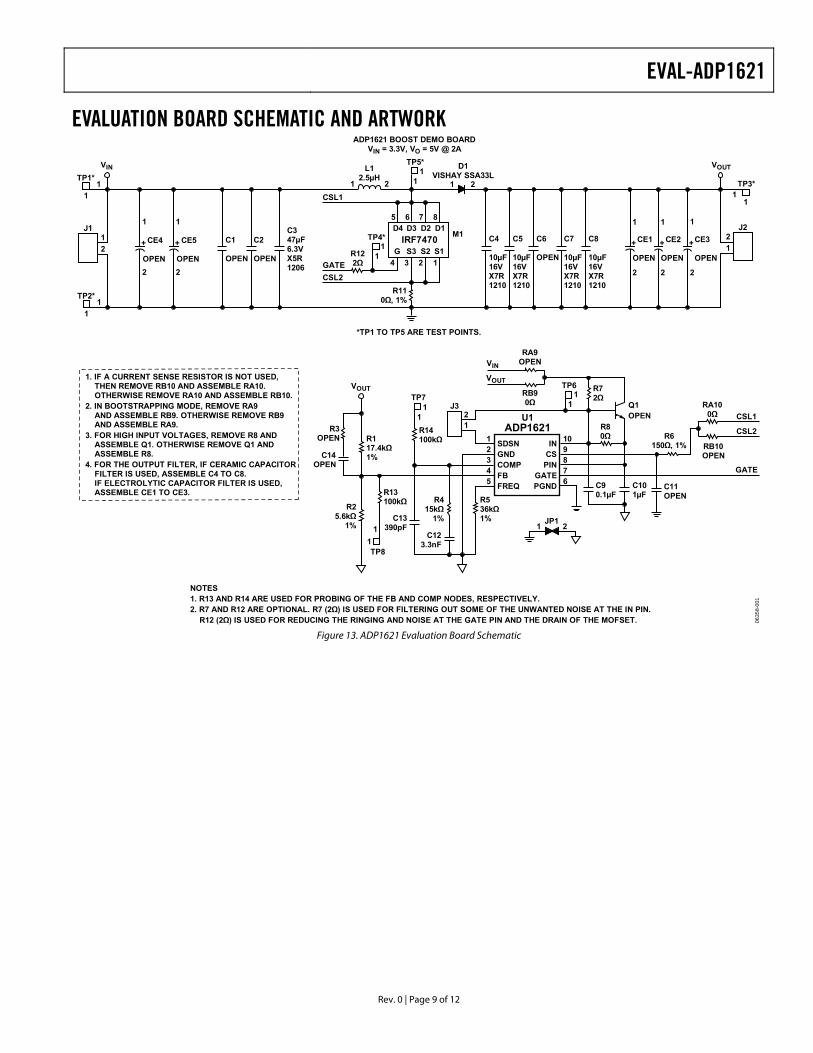
EVALUATION BOARD SCHEMATIC AND ARTWORK
0635
8-00
1
SDSNGNDCOMPFBFREQ
INCS
PINGATEPGND
U1ADP1621
R536kΩ1% JP11 2
R415kΩ
1%
C123.3nF
C13390pF
12345
TP7
21
J3
R14100kΩ
R13100kΩ
TP8
R25.6kΩ
1%
R117.4kΩ1%
R3OPEN
C14OPEN
VOUT
109876 C9
0.1µFC101µF
R80Ω
R72Ω
TP6
RA9OPEN
RB90Ω
VIN
VOUT
C11OPEN
R6150Ω, 1%
RA100Ω
RB10OPEN
CSL1
CSL2
GATE
Q1OPEN
111
1
11
1. IF A CURRENT SENSE RESISTOR IS NOT USED, THEN REMOVE RB10 AND ASSEMBLE RA10. OTHERWISE REMOVE RA10 AND ASSEMBLE RB10.2. IN BOOTSTRAPPING MODE, REMOVE RA9 AND ASSEMBLE RB9. OTHERWISE REMOVE RB9 AND ASSEMBLE RA9.3. FOR HIGH INPUT VOLTAGES, REMOVE R8 AND ASSEMBLE Q1. OTHERWISE REMOVE Q1 AND ASSEMBLE R8.4. FOR THE OUTPUT FILTER, IF CERAMIC CAPACITOR FILTER IS USED, ASSEMBLE C4 TO C8. IF ELECTROLYTIC CAPACITOR FILTER IS USED, ASSEMBLE CE1 TO CE3.
NOTES1. R13 AND R14 ARE USED FOR PROBING OF THE FB AND COMP NODES, RESPECTIVELY.2. R7 AND R12 ARE OPTIONAL. R7 (2Ω) IS USED FOR FILTERING OUT SOME OF THE UNWANTED NOISE AT THE IN PIN. R12 (2Ω) IS USED FOR REDUCING THE RINGING AND NOISE AT THE GATE PIN AND THE DRAIN OF THE MOFSET.
M1IRF7470
R110Ω, 1%
R122Ω
TP4*
GATECSL2
CSL1
TP5*L1
2.5µH1 2
D1VISHAY SSA33L
1 2
D4 D3 D2 D1
G S3 S2 S1
5 6 7 8
4 3 2 1
11
11
C347µF6.3VX5R1206
C2
OPEN
C1
OPEN
+ CE5
OPEN
+ CE4
OPEN
1
2
1
2
C6
OPEN
C5
10µF16VX7R1210
C4
10µF16VX7R1210
C8
10µF16VX7R1210
C7
10µF16VX7R1210
+ CE2
OPEN
+ CE1
OPEN
1
2
1
2
+CE3
OPEN
1
2
TP3*
11
VOUT
J2
12
J1
21
VINTP1*
11
TP2*
11
ADP1621 BOOST DEMO BOARDVIN = 3.3V, VO = 5V @ 2A
*TP1 TO TP5 ARE TEST POINTS.
Figure 13. ADP1621 Evaluation Board Schematic
EVAL-ADP1621
Rev. 0 | Page 10 of 12
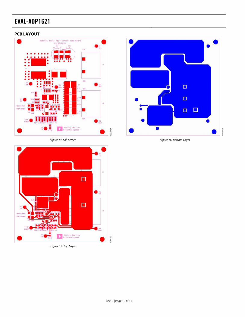
PCB LAYOUT
0635
8-01
6
0635
8-01
4
Figure 16. Bottom Layer Figure 14. Silk Screen
0635
8-01
5
Figure 15. Top Layer
EVAL-ADP1621
Rev. 0 | Page 11 of 12
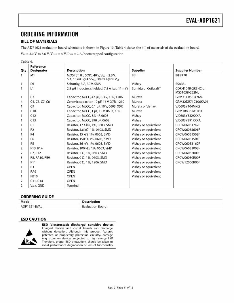
ORDERING INFORMATION BILL OF MATERIALS The ADP1621 evaluation board schematic is shown in Figure 13. Table 4 shows the bill of materials of the evaluation board.
VIN = 3.0 V to 3.6 V, VOUT = 5 V, IOUT = 2 A, bootstrapped configuration.
Table 4. Reference Designator Qty Description Supplier Supplier Number
1 M1 IRF IRF7470 MOSFET, 8 L SOIC, 40 V, VGS = 2.8 V, 5 A, 15 mΩ @ 4.5 VGS, 30 mΩ @2.8 VGS
1 D1 Schottky, 3 A, 30 V, SMA Vishay SSA33L 1 L1 2.5 μH inductor, shielded, 7.5 A Isat, 11 mΩ Sumida or Coilcraft® CDRH104R-2R5NC or
MSS1038-252NL 1 C3 Capacitor, MLCC, 47 μF, 6.3 V, X5R, 1206 Murata GRM31CR60J476M 4 C4, C5, C7, C8 Ceramic capacitor, 10 μF, 16 V, X7R, 1210 Murata GRM32DR71C106KA01 1 C9 Capacitor, MLCC, 0.1 μF, 10 V, 0603, X5R Murata or Vishay VJ0603Y104MXQ 1 C10 Capacitor, MLCC, 1 μF, 10 V, 0603, X5R Murata GRM188R61A105K 1 C12 Capacitor, MLCC, 3.3 nF, 0603 Vishay VJ0603Y332KXXA 1 C13 Capacitor, MLCC, 390 pF, 0603 Vishay VJ0603Y391KXXA 1 R1 Resistor, 17.4 kΩ, 1%, 0603, SMD Vishay or equivalent CRCW06031742F 1 R2 Resistor, 5.6 kΩ, 1%, 0603, SMD Vishay or equivalent CRCW06035601F 1 R4 Resistor, 15 kΩ, 1%, 0603, SMD Vishay or equivalent CRCW06031502F 1 R6 Resistor, 150 Ω, 1%, 0603, SMD Vishay or equivalent CRCW060315R1F 1 R5 Resistor, 36 kΩ, 1%, 0603, SMD Vishay or equivalent CRCW06033162F 2 R13, R14 Resistor, 100 kΩ, 1%, 0603, SMD Vishay or equivalent CRCW06031003F 2 R7, R12 Resistor, 2 Ω, 1%, 0603, SMD Vishay or equivalent CRCW06032R00F 3 R8, RA10, RB9 Resistor, 0 Ω, 1%, 0603, SMD Vishay or equivalent CRCW06030R00F 1 R11 Resistor, 0 Ω, 1%, 1206, SMD Vishay or equivalent CRCW12060R00F 1 R3 OPEN Vishay or equivalent 1 RA9 OPEN Vishay or equivalent 1 RB10 OPEN Vishay or equivalent 2 C11, C14 OPEN 2 VOUT, GND Terminal
ORDERING GUIDE Model Description ADP1621-EVAL Evaluation Board
ESD CAUTION

EVAL-ADP1621
Rev. 0 | Page 12 of 12
NOTES
©2006 Analog Devices, Inc. All rights reserved. Trademarks and registered trademarks are the property of their respective owners. EB06358-0-11/06(0)