Embed Size (px)
Citation preview

Evanescent Coupling Device Design forWaveguide-Integrated Group IV Photodetectors
The MIT Faculty has made this article openly available. Please share how this access benefits you. Your story matters.
Citation Donghwan Ahn, L.C. Kimerling, and J. Michel. “Evanescent CouplingDevice Design for Waveguide-Integrated Group IV Photodetectors.”Lightwave Technology, Journal of 28.23 (2010): 3387-3394. © 2010IEEE.
As Published http://dx.doi.org/10.1109/jlt.2010.2086433
Publisher Institute of Electrical and Electronics Engineers
Version Final published version
Citable link http://hdl.handle.net/1721.1/67499
Terms of Use Article is made available in accordance with the publisher'spolicy and may be subject to US copyright law. Please refer to thepublisher's site for terms of use.

JOURNAL OF LIGHTWAVE TECHNOLOGY, VOL. 28, NO. 23, DECEMBER 1, 2010 3387
Evanescent Coupling Device Design forWaveguide-Integrated Group IV Photodetectors
Donghwan Ahn, Member, IEEE, Lionel C. Kimerling, Senior Member, IEEE, and Jurgen Michel, Member, IEEE
Abstract—We have fabricated vertical p-i-n silicon photodetec-tors that are monolithically integrated with compact silicon-oxyni-tride channel waveguides. By comparing the evanescent couplingfrom low index-contrast waveguides and compact, high index-con-trast waveguides, the dependence of evanescent coupling behavioron the waveguide index and geometry designs was analyzed. Theeffects of fabrication variations in the coupling structure have beenstudied and it was found that an offsetting step in the waveguidecan help compensate for the mode mismatch at the transition in-terface from the input bus waveguide to the waveguide on top of thephotodetector. Finally, we present a design map, built by drawingthe evanescent coupling rate contour lines in the waveguide designspace, which well predicts the evanescent coupling trends.
Index Terms—Integrated optoelectronics, photodetectors,waveguides.
I. INTRODUCTION
S ILICON microphotonics has emerged with great interestrecently [1]–[3], due to its potential to enable large-scale
integration of photonic devices for applications such as low-costtelecommunication or on-chip optical interconnects. One of thekey elements for its success is the viable and efficient integrationof waveguide and high-performance photodetector.
Traditionally, waveguide-photodetector integration has beenprimarily focused on III-V compound semiconductor devices[4]–[7]. Only since 2007 have there been experimental reportsof waveguide-integrated germanium photodetectors [8]–[17].
In most III-V compound semiconductor-based waveguide-in-tegrated photodetectors [4]–[7], a bottom-waveguide-coupledstructure, where the evanescent-wave coupling occurs from abottom waveguide to an upper photodetector, has been a typicaldesign, as the waveguide and photodetector materials can be se-quentially grown by a heteroepitaxial process. The majority ofrecently-demonstrated Ge photodetectors integrated with a Siwaveguide also adopted this structure [9]–[13], [16]–[18] as thedirect epitaxy of germanium on Si can be utilized [19], [20].
Manuscript received May 01, 2010; revised August 13, 2010; acceptedAugust 30, 2010. Date of publication October 11, 2010; date of current versionNovember 24, 2010. This work was supported by the Defense AdvancedResearch Projects Agency’s (DARPA) EPIC Program supervised by Dr.Jagdeep Shah in the Microsysterms Technology Office (MTO) under ContractHR0011-05-C-0027.
D. Ahn was with Massachusetts Institute of Technology, Cambridge, MA02139 USA. He is now with Bell Laboratories, Alcatel-Lucent, Holmdel, NJ07733 USA.
L. C. Kimerling and J. Michel are with the Department of Materials Sci-ence and Engineering, Massachusetts Institute of Technology, Cambridge, MA02139 USA (e-mail: [email protected]).
Color versions of one or more of the figures in this paper are available onlineat http://ieeexplore.ieee.org.
Digital Object Identifier 10.1109/JLT.2010.2086433
On the other hand, a top-waveguide-coupled structure hasthe advantage of being flexible in choosing the waveguide ma-terial, unlike bottom-waveguide-coupled photodetector wherewaveguide material and substrate, on which the photodetector isepitaxially grown, have to be identical. A top-waveguide-cou-pled design also retains the general Si CMOS chip structurewhere active devices are fabricated on the substrate and the pas-sive interconnections are built in the upper levels. A top-wave-guide-coupled structure may fit better with the on-chip opticalinterconnection architectures where global optical interconnectsare envisioned to be located in or above the metal interconnectlevels [21], [22].
In our current work, we adopted a top-waveguide-coupledstructure and demonstrated the integrated structure of SiONchannel waveguides and Si photodetectors. There have beena few previous reports of Si photodetectors integrated withupper dielectric waveguides [23]–[26]. However, most of themexhibited slow evanescent coupling rates and amorphous [25]or polycrystalline [26] silicon detectors, which also sufferedfrom low responsivity and high bias voltage requirements. Inthis paper, we present crystalline p-i-n silicon photodetectorsintegrated with compact SiON channel waveguides, whichdemonstrated high coupling efficiency and high responsivitywith relatively small device size, due to high evanescent cou-pling rates.
A top-waveguide-integrated structure provides great flexi-bility in the materials choices and device designs. Therefore, itis critical to understand the coupling behavior dependency ondesign parameters and the resulting impact on photodetectorperformance, which were not addressed in previous studies[9]–[17], [23]–[26] as they reported on specific material anddesign choices. In this paper, we developed general designrules for waveguide-photodetector coupling by systematicallystudying the trend of change in the evanescent-wave couplingbehavior and device performance, as influenced by couplingstructure design and waveguide materials. The results willprovide useful information particularly for silicon micropho-tonics, where a large range of possible materials choices forwaveguides (SiO N –2.0), Si N , Si-richnitride , Si ) and photodetectors (Si, SiGe,and Ge) exist.
We furthermore developed a methodology that extracts keycoupling parameters such as coupling efficiency, coupling rate,and mode-matching parameters from the experimental measure-ment data as a function of photodetector coupling length, andstudied the change of such parameters as a result of waveguidedesign change. We also investigated mode-matching issues atthe entrance/exit interface between the photodetector and the
0733-8724/$26.00 © 2010 IEEE
3388 JOURNAL OF LIGHTWAVE TECHNOLOGY, VOL. 28, NO. 23, DECEMBER 1, 2010
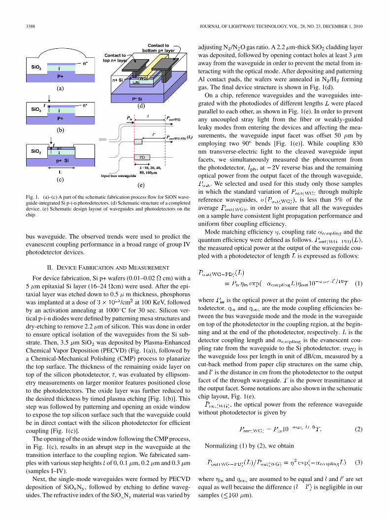
Fig. 1. (a)–(c) A part of the schematic fabrication process flow for SiON wave-guide-integrated Si p-i-n photodetectors. (d) Schematic structure of a completeddevice. (e) Schematic design layout of waveguides and photodetectors on thechip.
bus waveguide. The observed trends were used to predict theevanescent coupling performance in a broad range of group IVphotodetector devices.
II. DEVICE FABRICATION AND MEASUREMENT
For device fabrication, Si p+ wafers (0.01–0.02 cm) with a5 m epitaxial Si layer (16–24 cm) were used. After the epi-taxial layer was etched down to 0.5 m thickness, phosphoruswas implanted at a dose of /cm at 100 KeV, followedby an activation annealing at 1000 C for 30 sec. Silicon ver-tical p-i-n diodes were defined by patterning mesa structures anddry-etching to remove 2.2 m of silicon. This was done in orderto ensure optical isolation of the waveguides from the Si sub-strate. Then, 3.5 m SiO was deposited by Plasma-EnhancedChemical Vapor Deposition (PECVD) (Fig. 1(a)), followed bya Chemical-Mechanical Polishing (CMP) process to planarizethe top surface. The thickness of the remaining oxide layer ontop of the silicon photodetector, , was evaluated by ellipsom-etry measurements on larger monitor features positioned closeto the photodetectors. The oxide layer was further reduced tothe desired thickness by timed plasma etching [Fig. 1(b)]. Thisstep was followed by patterning and opening an oxide windowto expose the top silicon surface such that the waveguide couldbe in direct contact with the silicon photodetector for efficientcoupling [Fig. 1(c)].
The opening of the oxide window following the CMP process,in Fig. 1(c), results in an abrupt step in the waveguide at thetransition interface to the coupling region. We fabricated sam-ples with various step heights of 0, 0.1 m, 0.2 m and 0.3 m(samples I–IV).
Next, the single-mode waveguides were formed by PECVDdeposition of SiO N , followed by etching to define waveg-uides. The refractive index of the SiO N material was varied by
adjusting N /N O gas ratio. A 2.2 m-thick SiO cladding layerwas deposited, followed by opening contact holes at least 3 maway from the waveguide in order to prevent the metal from in-teracting with the optical mode. After depositing and patterningAl contact pads, the wafers were annealed in N /H forminggas. The final device structure is shown in Fig. 1(d).
On a chip, reference waveguides and the waveguides inte-grated with the photodiodes of different lengths were placedparallel to each other, as shown in Fig. 1(e). In order to preventany uncoupled stray light from the fiber or weakly-guidedleaky modes from entering the devices and affecting the mea-surements, the waveguide input facet was offset 50 m byemploying two 90 bends [Fig. 1(e)]. While coupling 830nm transverse-electric light to the cleaved waveguide inputfacets, we simultaneously measured the photocurrent fromthe photodetector, , at V reverse bias and the remainingoptical power from the output facet of the through waveguide,
. We selected and used for this study only those samplesin which the standard variation of through multiplereference waveguides, , is less than 5% of theaverage , in order to assure that all the waveguideson a sample have consistent light propagation performance anduniform fiber coupling efficiency.
Mode matching efficiency , coupling rate and thequantum efficiency were defined as follows. ,the measured optical power at the output of the waveguide cou-pled with a photodetector of length is expressed as follows:
(1)
where is the optical power at the point of entering the pho-todetector. and are the mode coupling efficiencies be-tween the bus waveguide mode and the mode in the waveguideon top of the photodetector in the coupling region, at the begin-ning and at the end of the photodetector, respectively. is thedetector coupling length and is the evanescent cou-pling rate from the waveguide to the Si photodetector. isthe waveguide loss per length in unit of dB/cm, measured by acut-back method from paper clip structures on the same chip,and is the distance in cm from the photodetector to the outputfacet of the through waveguide. is the power trasmittance atthe output facet. Some notations are also shown in the schematicchip layout, Fig. 1(e).
, the optical power from the reference waveguidewithout photodetector is given by
(2)
Normalizing (1) by (2), we obtain
(3)
where and are assumed to be equal and and are setequal as well because the difference is negligible in oursamples ( m).

AHN et al.: EVANESCENT COUPLING DEVICE DESIGN FOR WAVEGUIDE-INTEGRATED GROUP IV PHOTODETECTORS 3389
Fig. 2. (a) Normalized transmitted optical power and quantum efficiency vs.detector coupling length � from sample I (Table I). (b) Schematic of wave-guide photodetector coupling device structure and photon absorption process.(c) Intensity profile of scattered photons along the waveguide, taken from thetop-view CCD camera image of the sample.
Fig. 2(a) shows measurement data from sample I (a1.2 m 1.2 m waveguide with and a stepheight of m) in terms ofas a function of detector length . Five experimental datapoints were fitted to (3). The graph shows that incomingphotons from the input bus waveguide get coupled to themode in the waveguide on top of the photodetector with
% mode-matching efficiency and the optical powerin the waveguide on the photodetector decreases at a rate of
m due to the evanescent wave couplingto the Si photodetector.
We can also conclude that the total waveguide-to-photode-tector optical coupling efficiency, a measure that evaluates whatproportion of incoming photons from the input bus waveguideare successfully guided to the photodetector instead of beingscattered or lost to somewhere else, is well above 90%. Nearlyall photons that are coupled to the waveguide mode on top of thephotodetector will be coupled to the silicon pho-todetector via evanescent wave coupling in a sufficiently longphotodetector (e.g., )), and some portion
of the remaining 14% photons ) also can con-tribute to the photocurrent by being directly coupled to the Sidetector, as will be discussed further later.
The quantum efficiency is defined as follows:
(4)
The measured quantum efficiency data as a function ofdetector length are shown in Fig. 2(a). In determining afitting function, we need to consider that there are multiplepaths a photon can take until eventually being absorbed in theSi layer and that each path has a different dependence of thephotocurrent on the detector length . We define three couplingmechanisms.
Mechanism I: This mechanism occurs when the photonsin the input bus waveguide reaches the Si detector. Modematching conditions between the waveguide mode and Si radi-ation modes allow photons to couple directly into the Si layer.This mechanism also describes scattering into the Si layer dueto the abrupt effective index change in the bus waveguide.Contribution to photocurrent, resulting from Mechanism I,
can be expressed as follows:
(5)
where is the undetermined ratio of the photons coupled to sil-icon to the photons that did not couple to the waveguide modeon top of the photodetector. is the internal responsivity of thedetector resulting from this process. Since absorption is a func-tion of path length in silicon, is the function that increasesfrom zero and saturates at 1 with detector length . Since Mech-anism I consists of many different absorption paths, ,and should reflect the combined effect of each absorptionprocess.
Mechanism II: Evanescent wave coupling process. The lightthat remains in the waveguide on top of the photodetector willcouple to the Si photodetector at a constant rate. Therefore, thephotocurrent from Mechanism II can be written as
(6)
where is the responsivity of the photodetector at 830 nm.Mechanism III: At the end of the Si photodetector, the re-
maining light in the waveguide experiences a modal disconti-nuity because of the abrupt change in structures and effectiveindex. Part of the light that is still remaining in the waveguidecan be scattered back into the Si layer.
Contributions to photocurrent from Mechanism III should besignificantly smaller than from Mechanisms I and II. The pho-tocurrent due to Mechanism I levels off much more quickly withdetector length than the photocurrent due to Mechanism II, be-cause the coupling to silicon in Mechanism I occurs nearly in-stantly at the input interface of the photodetector and the absorp-tion length inside silicon in the lateral direction, , cannotexceed , which is about 14 m at 830 nm. Therefore, we

3390 JOURNAL OF LIGHTWAVE TECHNOLOGY, VOL. 28, NO. 23, DECEMBER 1, 2010
TABLE ISUMMARY OF DEVICE SAMPLE DESIGNS AND MEASURED/ANALYZED PERFORMANCE DATA
can create a simplified equation by assuming that the photocur-rent from Mechanism I is approximately constant. Therefore
(7)
The term represents the saturated quantum efficiencywhen the photodetector length is sufficiently large. In ad-dition, can be used as a parameter that indicateshow dominant Mechanism I is, compared to the other two cou-pling mechanisms, and in turn shows how large the mode-mis-match between the input bus waveguide and the waveguide onthe photodetector is. These parameters for sample A are shownin Fig. 2(a). We used various sample sets with three differentwaveguide designs and additional step height variations. Themeasured and fitted data are summarized in Table I.
III. EFFECT OF STEP HEIGHT VARIATION
As Fig. 2(c) shows, Mechanisms I and III contain photon scat-tering due to the mode-mismatch between input or output buswaveguide and the waveguide on top of the photodetector in thecoupling region. In general, it is desirable to minimize photonscattering in order to reduce optical energy loss and prevent car-rier generation due to scattered photons in nearby devices. Wetherefore studied the influence of the step height [see Fig. 1(c)]on the scattering loss. Comparison between samples with iden-tical waveguide design but varying step heights (samples I–IVin Table I) shows the maximum mode-matching efficiency pa-rameter for the sample with m (Sample II). More ap-parently, the value of the mode-mismatch indicator ,as defined in Fig. 2(a) and re-plotted as a function of step height
in Fig. 3, reaches a minimum when m. This resultshows that more optical power from the input bus waveguide iscoupled into the mode in the waveguide on the photodetector,when a 0.2 m step is intentionally introduced at the interfacewhere the bus waveguide reaches the photodetector.
We can analytically calculate and compare the mode profileof the waveguide in the input bus region and that in the photode-tector-coupled region, as shown in Fig. 4.
Fig. 3. Mode-mismatch indicator ���� � ��, as defined in Fig. 4, from thesamples with different step height �.
Fig. 4. The mode profiles calculated in a multilayer structure where the wave-guide material is in contact with the bottom oxide cladding layer (dashed line,� ) or silicon absorbing layer (solid line, � ). As an approximation, the 1Dmultilayer structure was obtained by applying the Effective Index Method (EIM)to 2D waveguide structure. The transfer matrix method with complex refractiveindexes [27] was used for mode calculations. The inset shows the change ofoverlap integral between � and � as a function of the mode offset �.
According to Fig. 4, the leaky mode in the waveguide onthe Si photodetector has zero electric field at the inter-face between waveguide core material and the underlying sil-icon and its overall position is shifted away from the silicon pho-todetector, increasing the mode-mismatch with the symmetricalmode profile of the input bus waveguide .

AHN et al.: EVANESCENT COUPLING DEVICE DESIGN FOR WAVEGUIDE-INTEGRATED GROUP IV PHOTODETECTORS 3391
Fig. 5. 3D FDTD side-section views of photon propagation in the couplingstructure where waveguide has (a) no step and (b) � � ��� �m abrupt step as itenters the coupling region.
The overlap integral between these two modes can be calcu-lated with the following equation:
(8)
Then, replacing with in the above equation,we can estimate the dependence of the mode overlap integral asa function of the mode offset . The inset of Fig. 4 shows thatthe mode offset of 0.23 m can increase the mode-matchingbetween the two modes by about 5.5%. This mode offset can beimplemented in the device fabrication process by introducing acontrolled step height in the waveguide at the transition to thecoupling region [Fig. 1(c)].
The experimental observations and analytical estimations ofthe coupling offset are also supported by optical simulations.3D finite-difference time-domain (FDTD) simulation results inFig. 5(a) show that the propagation mode in the waveguide ex-periences an upward shift as it enters the coupling region. Incontrast, optical simulation with a step of 0.2 m in the wave-guide as shown in Fig. 5(b) demonstrate that the light propaga-tion mode experiences less disruption as it enters the couplingregion and scattering losses are reduced.
This effect applies to a broad range of integrated pho-todetector designs, especially the ones in which CouplingMechanism II is important. The optimal step height in thephotodetector device with different design parameters (wave-length, refractive index, etc.) can be generally calculated in thesame way as described above.
IV. EVANESCENT COUPLING DESIGN MAP
The device sample sets presented in this paper had signifi-cant variations of the waveguide index-contrast
Fig. 6. (a) Measured (symbols) and fitted (lines) data of quantum efficiencyof waveguide-integrated photodetector as a function of detector couplinglength. Comparison between the device samples based on the same siliconphotodetector, but coupled with low �� vs. high �� waveguides, and thenon-waveguide-coupled device with surface-normal illumination is shown.Also, data from Ge photodetector coupled with silicon nitride waveguides(�� � ����, [8]), though measured at 1550 �m, demonstrates nice extensionof the trend to very high index-contrast regime. (b)–(c) Cross-section view ofoptical simulation, immediately (at 0.5 �m) after the coupling region to thephotodetector begins, for the device coupled with high �� ((b)) vs. low ��
((c)) waveguide.
), the main parameter of waveguide design, from low(samples I–IV in Table I) to relatively high values (samplesV, VI). The measured quantum efficiency data from varioussample sets as functions of waveguide-detector coupling lengthare drawn in Fig. 6(a).
A clear trend of quantum efficiency saturation dependencyon different waveguide designs is that, as the index-contrast
of single-mode waveguides increases, the quantum effi-ciency tends to saturate more quickly within shorter detectorcoupling length and the parameter , defined in(7) and Fig. 2(a), increases. Increasing value ofin higher waveguides indicates relative dominance ofcoupling Mechanism I, which is also verified from Fig. 6(b) incomparison to Fig. 6(c). Coupling Mechanism I is responsiblefor enhanced total quantum efficiency through direct opticalcoupling from the bus waveguide to the modes inside theSi photodetector and thus enables the high waveguideintegrated photodetector to achieve the efficiency well beyondthat of surface-illuminated photodetector devices. The detailedexplanation and supporting evidences for the physical back-ground for this trend were previously reported in [28].
The experimental results in this paper clearly show that thedifference in waveguide design, even if integrated with the sameSi photodetectors, significantly changes the evanescent couplingphenomenon and the overall device performances. Therefore itis worthwhile to generalize the observed trends in an extendeddesign map and understand key design factors in evanescentcoupling device design.
The two most significant design factors that are consideredin the waveguide design process would be 1) the choice ofwaveguide core material (SiO cladding is given in most groupIV photonic devices) and 2) the determination of waveguidegeometry and dimension. The first factor can be parameterized
3392 JOURNAL OF LIGHTWAVE TECHNOLOGY, VOL. 28, NO. 23, DECEMBER 1, 2010
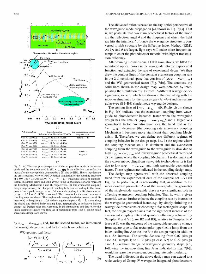
Fig. 7. (a) The ray-optics perspective of the propagation mode in the wave-guide and the notations used in (9). � is the effective core refractiveindex after the waveguide is converted to a 2D slab by EIM. Shown together arethe cross-sectional view of FDTD optical simulation of the coupling structureof a 0.9 �m� 0.9 �m SiON �� � ����� waveguide and a Si photode-tector. The dotted arrow and solid arrows in the Si photodetector area representthe Coupling Mechanism I and II, respectively. (b) The evanescent couplingdesign map showing the change of coupling behavior, according to the varia-tions of waveguide design. � � �� nm and coupling to a Si photodetector�� � ��� � ��� is assumed. The contours for the same evanescentcoupling rates are shown. The single-mode waveguide designs (near cut-off di-mensions) with square �� � �� and rectangular shape ���� � � move alongthe dotted and dashed index-scaling lines, respectively, as refractive indiceschange. (c) Design cases that were used in the simulations and that follow theindex-scaling of square-type (line A) or rectangular-type (line B) single modewaveguide designs are shown.
by and, for the second factor, we introducedthe waveguide geometrical factor, which we define as
WG geometrical factor
(9)
The above definition is based on the ray-optics perspective ofthe waveguide mode propagation [as shown in Fig. 7(a)]. Thatis, we postulate that two main geometrical factors of the modeare the reflection angel and the frequency at which the lightray hits the interface, , once the waveguide structure is con-verted to slab structure by the Effective Index Method (EIM).As and are larger, light rays will make more frequent at-tempt to enter the photodetector material with higher transmis-sion efficiency.
After running 3-dimensional FDTD simulations, we fitted themonitored optical power in the waveguide into the exponentialfunction and extracted the rate of exponential decay. We thendrew the contour lines of the constant evanescent coupling ratein the 2 dimensional space that consists ofand the WG geometrical factor [Fig. 7(b)]. The contours, thesolid lines shown in the design map, were obtained by inter-polating the simulation results from 16 different waveguide de-sign cases, some of which are shown in the map along with theindex-scaling lines for the square-type (A1–A4) and the rectan-gular-type (B1–B4) single-mode waveguide designs.
The contour lines of m shownin Fig. 7(b) indicate that the evanescent coupling from wave-guide to photodetector becomes faster when the waveguidedesign has the smaller and a larger WGgeometrical factor. We also have seen the trend that as the
decreases (the coupling rate increases), couplingMechanism I becomes more significant than coupling Mech-anism II. Therefore, we can define two different regimes ofcoupling behavior in the design map, i.e., 1) the regime wherethe coupling Mechanism II is dominant and the evanescentcoupling from the waveguide to the waveguide is slow due tohigh and low waveguide geometrical factor and2) the regime where the coupling Mechanism I is dominant andthe evanescent coupling from waveguide to photodetector is fastdue to low and high waveguide geometricalfactor. These regimes are indicated in the coupling design map.
The design map agrees well with the observed couplingtrend from the experimental data of the Sample set I–VI (inFig. 6). In particular, it is noteworthy that, in addition to theindex-contrast parameter of the waveguide, the geometryof the single-mode waveguide plays a very significant role inaffecting evanescent coupling behavior. That is, with a givenmaterial, we can further enhance the coupling rate by increasingthe waveguide geometrical factor, e.g., by simply shrinking thewaveguide dimensions or choosing a flat rectangular shape. Infact, the design map explains that the significant increase of theevanescent coupling rate and quantum efficiency achieved bySamples V and VI (case B2 and B3), relative to Samples I–IV(case A1), was the outcome of the waveguide geometry changefrom square-type to flat-rectangular type (i.e., a jump from theindex-scaling line A to the line B in the design map), in additionto a increase. The simple scaling from 0.07 (designcase A1, sample I) to 0.12 (design case A2) to 0.22 (designcase A3) without change of waveguide geometry shape [i.e.,following the index-scaling line A as indicated in Fig. 7(b)],would increase the evanescent coupling rate only modestly.
The trend indicated in the above design map can extend to awide variety of Group IV waveguide-integrated photodetectors

AHN et al.: EVANESCENT COUPLING DEVICE DESIGN FOR WAVEGUIDE-INTEGRATED GROUP IV PHOTODETECTORS 3393
Fig. 8. 3D FDTD side-section view of photon propagation in the couplingstructure where (a) 3.5 �m vs. (b) 0.4 �m thick Ge photodetector is placed onSi channel waveguide and (c) 0.8 �m thick Ge photodetector is placed on Si ribwaveguide structure [10]. Ge absorption coefficient of � � ������� �mat � � ���� nm was assumed for simulation.
and even beyond the shown 850 nm wavelength cases. For ex-ample, as we continue moving in the direction towards highand larger WG geometrical factor, one of the extreme experi-mental cases would be the sub-micron scale, Si channel wave-guide coupled to a Ge photodetector [11]–[13], [16]–[18], [29].Such structures have very low of 0.5 and avery high waveguide geometrical factor because of thehigh refractive index of the silicon waveguide core and the verysmall, flat rectangular single-mode waveguide dimensions (e.g.,500 nm (W) 200 nm (H)). Just as the above design map helpsus anticipate very fast, nearly Mechanism I dominant couplingfor such structures, the simulation in Fig. 8(a) shows the photonsfrom Si channel WG couple to Ge PD almost immediately at theonset of the detector coupling. In case of the thin-film Ge pho-todetector [i.e., (absorption length of Ge)], thecoupling to a Ge photodetector is still immediate at the onsetof the detector coupling, but, because a single pass of photonsinside Ge layer is not enough to absorb all the photons, the un-absorbed photons are reflected back into silicon. They continuepropagation while oscillating between the Si and Ge layer untilbeing fully absorbed (Fig. 8(b) [30]), extending the couplinglength to 10 m. This behavior was experimentally confirmedby our previous report on Ge photodetectors vertically coupledto Si channel waveguides [18], which showed that all photonswere coupled and absorbed within 5 m length (or within 20
m at longer wavelength beyond the Ge direct bandgap whereabsorption in Ge becomes less efficient).
Meanwhile, other research groups have strategically adoptedSi rib waveguides as their building blocks for silicon-based pho-tonic chips [10], [31], [32]. Single-mode rib waveguide designhas its effective index very close to the core refractive index,as nearly all of the waveguide mode is contained in the wave-guide core material, and has relatively large waveguide dimen-
sions. Such characteristics of Si rib waveguide design lead tovery small waveguide geometrical factors ( for the designused in [10], i.e., much smaller than any channel waveguide de-signs we considered in our experiments and simulations). Beingplaced at the left end of the design map (Fig. 7(b)), in opposi-tion to Si channel waveguide design, Si rib waveguides are ex-pected to have slow evanescent coupling rates when integratedto Ge photodetectors. In addition to our simulation result forsuch structure (Fig. 8(c)), the experimental report by Intel re-searchers [10] indicated their devices required the detector cou-pling length of about 100 m for full responsivity saturation.Their unique results, different from faster responsivity satura-tion within short coupling length in other Ge photodetectors in-tegrated Si channel waveguides, are well explained by the cou-pling behavior trend identified in our design map, Fig. 7.
V. CONCLUSION
We have demonstrated waveguide-integrated silicon photode-tectors that employ a top-to-bottom evanescent-wave couplingstructure. We achieved over 90% coupling efficiency from SiONwaveguides to Si photodetectors. We identified three differentcoupling mechanisms and investigated the impact of the couplingdevice design on the coupling mechanisms. A two-step processthat consists of 1) mode-coupling from a guided mode in theinput bus waveguide to a leaky mode in the waveguide on topof the photodetector and 2) gradual evanescent wave couplingfrom the waveguide into the photodetector, was a main cou-pling mechanism in the case of devices with low index-contrastwaveguides. Such designs with low index-contrast waveguideswith small waveguide geometrical factors will be useful forapplications like optical power taps, due to slower evanescentcoupling rates in the coupling regionandefficient mode-couplingat the entrance of the photodetector between input bus waveguideand the waveguide on top of the photodetector. We showed thatintentional introduction of a step in the input bus waveguide as itenters the Si photodetector further improves the mode-matchingefficiency between the input bus waveguide and the waveguideon top of the photodetector. The total quantum efficiency of theintegrated photodetector ( – % for the low index-contrastwaveguide) was limited by partial collectionofcarriers generatedby the evanescently coupled photons in the silicon photodetector( % quantum efficiency with 830nm surface-normal illumi-nation). In the case of high index-contrast waveguides with largewaveguide geometrical factor, coupling to the photodetectoroccurred mainly by mode matching of the input waveguide modeand radiation modes in the Si photodetector, leading to 78%quantum efficiency. The coupling structure designs with highindex-contrast waveguides may serve well for end-node pho-todetectors that require short coupling length for high bandwidth.
We built a design map, which maps out the key single-modewaveguide materials and geometrical design factors onto 2-di-mensional space and visualizes the trend of evanescent couplingbehavior change as a result of waveguide designs. In addition togood agreement with the trend found in different kinds of SiONwaveguide-integrated Si photodetector device sets we demon-strated in this paper, the design map well explains the evanes-cent coupling trend in a wide variety of group IV waveguide-in-tegrated photodetector.
3394 JOURNAL OF LIGHTWAVE TECHNOLOGY, VOL. 28, NO. 23, DECEMBER 1, 2010
REFERENCES
[1] L. C. Kimerling, L. D. Negro, S. Saini, Y. Yi, D. Ahn, S. Akiyama, D.Cannon, J. Liu, J. G. Sandland, D. Sparacin, J. Michel, K. Wada, and M.R. Watts, “Monolithic silicon microphotonics,” in Silicon Photonics,ser. Topics in Applied Physics, L. Pavesi and D. J. Lockwood, Eds.,1st ed. Berlin, Germany: Springer-Verlag, 2006, pp. 89–119, no. 94.
[2] R. Kirchain and L. Kimerling, “A roadmap for nanophotonics,” NatPhoton, vol. 1, no. 6, pp. 303–305, 2007.
[3] “Silicon photonics and photonic integrated circuits II,” in Proc. SPIE,G. C. Righini, Ed., May 2010, vol. 7719.
[4] M. Erman, P. Jarry, R. Gamonal, J.-L. Gentner, P. Stephan, and C.Guedon, “Monolithic integration of a GaInAs p-i-n photodiode andan optical waveguide: modeling and realization using chloride vaporphase epitaxy,” J. Lightw. Technol., vol. 6, no. 3, pp. 399–412, Mar.1988.
[5] R. Deri, W. Doldissen, R. Hawkins, R. Bhat, J. Soole, L. Schiavone, M.Seto, N. Andreadakis, Y. Silberberg, and M. Koza, “Efficient verticalcoupling of photodiodes to InGaAsP rib waveguides,” Appl. Phys. Lett.,vol. 58, no. 24, pp. 2749–2751, June 1991.
[6] J. Vinchant, F. Mallecot, D. Decoster, and J. Vilcot, “Photodetectorsmonolithically integrated with optical waveguides: Theoretical and ex-perimental study of absorbing layer effects,” Proc. Inst. Electr. Eng.—Optoelectron., vol. 136, no. 1, pp. 72–75, 1989.
[7] Y.-S. Wu, J.-W. Shi, J.-Y. Wu, F.-H. Huang, Y.-J. Chan, Y.-L. Huang,and R. Xuan, “High-performance evanescently edge coupled photodi-odes with partially p-doped photoabsorption layer at 1.55 �m wave-length,” IEEE Photon. Technol. Lett., vol. 17, no. 4, pp. 878–880, Apr.2005.
[8] D. Ahn, C.-Y. Hong, J. Liu, W. Giziewicz, M. Beals, L. Kimerling, J.Michel, J. Chen, and F. Kartner, “High performance, waveguide inte-grated Ge photodetectors,” Opt. Exp., vol. 15, no. 7, pp. 3916–3921,Apr. 2007.
[9] L. Vivien, M. Rouvicre, J. Fedeli, D. Marris-Morini, J. Damlencourt, J.Mangeney, P. Crozat, L. E. Melhaoui, E. Cassan, X. L. Roux, D. Pascal,and S. Laval, “High speed and high responsivity germanium photode-tector integrated in a silicon-on-insulator microwaveguide,” Opt. Exp.,vol. 15, pp. 9843–9848, 2007.
[10] T. Yin, R. Cohen, M. Morse, G. Sarid, Y. Chetrit, D. Rubin, and M.Paniccia, “31 GHz Ge nip waveguide photodetectors on silicon-on-in-sulator substrate,” Opt. Exp., vol. 15, no. 21, pp. 13965–13971, 2007.
[11] J. Wang, W. Y. Loh, K. T. Chua, H. Zang, Y. Z. Xiong, T. H. Loh, M.B. Yu, S. J. Lee, G.-Q. Lo, and D.-L. Kwong, “Evanescent- coupledGe p-i-n photodetectors on Si-waveguide with SEG-Ge and compara-tive study of lateral and vertical p-i-n configurations,” IEEE ElectronDevice Lett., vol. 29, no. 5, pp. 445–448, May 2008.
[12] L. Chen, P. Dong, and M. Lipson, “High performance germanium pho-todetectors integrated on submicron silicon waveguides by low tem-perature wafer bonding,” Opt. Exp., vol. 16, no. 15, pp. 11513–11518,2008.
[13] V. Sorianello, M. Balbi, L. Colace, G. Assanto, L. Socci, L. Bolla, G.Mutinati, and M. Romagnoli, “Guided-wave photodetectors in germa-nium on SOI optical chips,” Physica E, vol. 41, no. 6, pp. 1090–1093,2009.
[14] D. Feng, S. Liao, P. Dong, N.-N. Feng, H. Liang, D. Zheng, C.-C.Kung, J. Fong, R. Shafiiha, J. Cunningham, A. Krishnamoorthy, andM. Asghari, “High-speed Ge photodetector monolithically integratedwith large cross-section silicon-on-insulator waveguide,” Appl. Phys.Lett., vol. 95, no. 26, pp. 261105–3, Dec. 2009.
[15] S. Assefa, F. Xia, S. Bedell, Y. Zhang, T. Topuria, P. Rice, and Y.Vlasov, “CMOS-integrated high-speed MSM germanium waveguidephotodetector,” Opt. Exp., vol. 18, no. 5, pp. 4986–4999, 2010.
[16] K.-W. Ang, J. W. Ng, A. E.-J. Lim, M.-B. Yu, G.-Q. Lo, and D.-L.Kwong, “Waveguide-integrated Ge/Si avalanche photodetector with105 GHz gain-bandwidth product,” in Proc. OFC/NFOEC, 2010,Paper JWA36.
[17] Q. Fang, T.-Y. Liow, J. Song, K. Ang, M. Yu, G. Lo, and D.-L. Kwong,“WDM multi-channel silicon photonic receiver with 320 Gbps datatransmission capability,” Opt. Exp., vol. 18, no. 5, pp. 5106–5113,2010.
[18] J. Liu, D. Ahn, C. Y. Hong, D. Pan, S. Jongthammanurak, M. Beals,L. C. Kimerling, J. Michel, A. T. Pomerene, D. Carothers, C. Hill,M. Jaso, K. Y. Tu, Y. K. Chen, S. Patel, M. Rasras, D. M. Gill, andA. E. White, “Waveguide integrated Ge p-i-n photodetectors on a sil-icon-on-insulator platform,” in Proc. Opt. Valley of China Int. Symp.Optoelectron., 2006, pp. 1–4.
[19] H.-C. Luan, D. Lim, K. Lee, K. Chen, J. Sandland, K. Wada, and L.Kimerling, “High-quality Ge epilayers on Si with low threading-dis-location densities,” Appl. Phys. Lett., vol. 75, no. 19, pp. 2909–2911,Nov. 1999.
[20] Z. Huang, J. Oh, S. K. Banerjee, and J. C. Campbell, “Effectivenessof SiGe buffer layers in reducing dark currents of Ge-on-Si photode-tectors,” IEEE J. Quantum Electron., vol. 43, no. 3, pp. 238–242, Mar.2007.
[21] S. Tewksbury and L. Hornak, “Optical clock distribution in electronicsystems,” J. VLSI Signal Process., vol. 16, no. 2, pp. 225–246, June1997.
[22] V. Stenger and F. Beyette, “Design and analysis of an optical wave-guide tap for silicon CMOS circuits,” J. Lightw. Technol., vol. 20, no.2, pp. 277–284, Feb. 2002.
[23] S. Wunderlich, J. Schmidt, and J. Muller, “Integration of SiON waveg-uides and photodiodes on silicon substrates,” Appl. Opt., vol. 31, no.21, pp. 4186–4189, July 1992.
[24] U. Hilleringmann and K. Goser, “Optoelectronic system integration onsilicon: Waveguides, photodetectors, and VLSI CMOS circuits on onechip,” IEEE Trans. Electron Devices, vol. 42, no. 5, pp. 841–846, May1995.
[25] K. Kapser and P. Deimel, “Lateral coupling between a silicon-oxini-tride waveguide and an amorphous Si photodiode,” J. Appl. Phys., vol.71, no. 7, pp. 3614–3616, Apr. 1992.
[26] G. Yuan, R. Pownall, P. Nikkel, C. Thangaraj, T. Chen, and K.Lear, “Characterization of CMOS compatible waveguide-coupledleaky-mode photodetectors,” IEEE Photon. Technol. Lett., vol. 18, no.15, pp. 1657–1659, Aug. 2006.
[27] K. Schlereth and M. Tacke, “The complex propagation constant of mul-tilayer waveguides: An algorithm for a personal computer,” IEEE J.Quantum Electron., vol. 26, no. 4, pp. 627–630, Apr. 1990.
[28] D. Ahn, C.-Y. Hong, L. C. Kimerling, and J. Michel, “Coupling effi-ciency of monolithic, waveguide-integrated Si photodetectors,” Appl.Phys. Lett., vol. 94, no. 8, Jan. 2009, Art. ID 081108.
[29] J. Michel, J. Liu, D. Ahn, D. Sparacin, R. Sun, C. Hong, W. Giziewicz,M. Beals, L. Kimerling, A. Kopa, A. Apsel, M. Rasras, D. Gill, S. Patel,K. Tu, Y. Chen, A. White, A. Pomerene, D. Carothers, and M. Grove,“Advances in fully CMOS integrated photonic devices,” Proc. SPIE,vol. 6477, no. 1, pp. 64 770P–11, Feb. 2007.
[30] M. Rouviere, M. Halbwax, J. Cercus, E. Cassan, L. Vivien, D. Pascal,M. Heitzmann, J. Hartmann, and S. Laval, “Integration of germaniumwaveguide photodetectors for intrachip optical interconnects,” Opt.Eng., vol. 44, 2005, Art. ID 075402.
[31] A. Liu, H. Rong, R. Jones, O. Cohen, D. Hak, and M. Paniccia, “Op-tical amplification and lasing by stimulated Raman scattering in siliconwaveguides,” J. Lightw. Technol., vol. 24, no. 3, pp. 1440–1455, Mar.2006.
[32] B. Smith, D. Feng, H. Lei, D. Zheng, J. Fong, P. Zhou, and M. As-ghari, “Progress in manufactured silicon photonics,” in Proc. SPIE,Feb. 2007, vol. 6477, no. 1, Art. ID 647702.
Author biographies not included at authors’ request due to spaceconstraints.