Embed Size (px)
DESCRIPTION
wikipedia doc
Citation preview
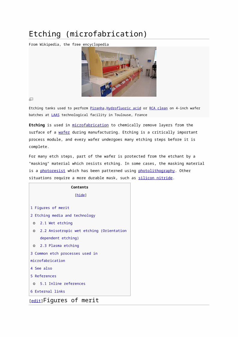
Etching (microfabrication)From Wikipedia, the free encyclopedia
Etching tanks used to perform Piranha,Hydrofluoric acid or RCA clean on 4-inch wafer batches at LAAS technological
facility in Toulouse, France
Etching is used in microfabrication to chemically remove layers from the surface of a wafer during
manufacturing. Etching is a critically important process module, and every wafer undergoes many etching
steps before it is complete.
For many etch steps, part of the wafer is protected from the etchant by a "masking" material which resists
etching. In some cases, the masking material is a photoresist which has been patterned
using photolithography. Other situations require a more durable mask, such as silicon nitride.
Contents
[hide]
1 Figures of merit
2 Etching media and technology
o 2.1 Wet etching
o 2.2 Anisotropic wet etching (Orientation dependent etching)
o 2.3 Plasma etching
3 Common etch processes used in microfabrication
4 See also
5 References
o 5.1 Inline references
6 External links
[edit]Figures of merit
If the etch is intended to make a cavity in a material, the depth of the cavity may be controlled
approximately using the etching time and the known etch rate. More often, though, etching must entirely
remove the top layer of a multilayer structure, without damaging the underlying or masking layers. The
etching system's ability to do this depends on the ratio of etch rates in the two materials (selectivity).

Some etches undercut the masking layer and form cavities with sloping sidewalls. The distance of
undercutting is called bias. Etchants with large bias are called isotropic, because they erode the substrate
equally in all directions. Modern processes greatly prefer anisotropic etches, because they produce sharp,
well-controlled features.
Selectivity
Yellow: layer to be removed; blue: layer to remain
1. A poorly selective etch removes the top layer, but also attacks
the underlying material.
2. A highly selective etch leaves the underlying material
unharmed.
Isotropy
Red: masking layer; yellow: layer to be removed
1. A perfectly isotropic etch produces round sidewalls.
2. A perfectly anisotropic etch produces vertical sidewalls.
[edit]Etching media and technology
The two fundamental types of etchants are liquid-phase ("wet") and plasma-phase ("dry"). Each of these
exists in several varieties.
[edit]Wet etching

Radiation hardened die of the 1886VE10microcontroller prior to metalization etching
Radiation hardened die of the 1886VE10microcontroller after a metalization etching process has been used
The first etching processes used liquid-phase ("wet") etchants. The wafer can be immersed in a bath of
etchant, which must be agitated to achieve good process control. For instance, buffered hydrofluoric
acid (BHF) is used commonly to etch silicon dioxide over a silicon substrate.
Different specialised etchants can be used to characterise the surface etched.
Wet etchants are usually isotropic, which leads to large bias when etching thick films. They also require the
disposal of large amounts of toxic waste. For these reasons, they are seldom used in state-of-the-art
processes. However, the photographic developer used for photoresist resembles wet etching.
As an alternative to immersion, single wafer machines use the Bernoulli principle to employ a gas (usually,
pure nitrogen) to cushion and protect one side of the wafer while etchant is applied to the other side. It can
be done to either the front side or back side. The etch chemistry is dispensed on the top side when in the
machine and the bottom side is not affected. This etch method is particularly effective just before "backend"
processing (BEOL), where wafers are normally very much thinner after wafer backgrinding, and very
sensitive to thermal or mechanical stress. Etching a thin layer of even a few micrometres will remove
microcracks produced during backgrinding resulting in the wafer having dramatically increased strength
and flexibility without breaking.
[edit]Anisotropic wet etching (Orientation dependent etching)

An anisotropic wet etch on a silicon wafer creates a cavity with a trapezoidal cross-section. The bottom of the cavity is a
{100} plane (see Miller indices), and the sides are {111} planes. The blue material is an etch mask, and the green
material is silicon.
Some wet etchants etch crystalline materials at very different rates depending upon which crystal face is
exposed. In single-crystal materials (e.g. silicon wafers), this effect can allow very high anisotropy, as
shown in the figure.
Several anisotropic wet etchants are available for silicon, all of them hot aqueous caustics. For
instance, potassium hydroxide (KOH) displays an etch rate selectivity 400 times higher in <100> crystal
directions than in <111> directions. EDP (an aqueous solution of ethylene diamine and pyrocatechol),
displays a <100>/<111> selectivity of 17X, does not etch silicon dioxide as KOH does, and also displays
high selectivity between lightly doped and heavily boron-doped (p-type) silicon. Use of these etchants on
wafers that already contain CMOS integrated circuits requires protecting the circuitry. KOH may introduce
mobile potassium ions into silicon dioxide, and EDP is highly corrosive and carcinogenic, so care is
required in their use.Tetramethylammonium hydroxide (TMAH) presents a safer alternative than EDP, with
a 37X selectivity between {100} and {111} planes in silicon.
Etching a (100) silicon surface through a rectangular hole in a masking material, for example a hole in a
layer of silicon nitride, creates a pit with flat sloping {111}-oriented sidewalls and a flat (100)-oriented
bottom. The {111}-oriented sidewalls have an angle to the surface of the wafer of:
If the etching is continued "to completion", i.e. until the flat bottom disappears, the pit becomes a
trench with a V-shaped cross section. If the original rectangle was a perfect square, the pit when
etched to completion displays a pyramidal shape.
The undercut, δ, under an edge of the masking material is given by:
,
where Rxxx is the etch rate in the <xxx> direction, T is the etch time, D is the etch depth and S is
the anisotropy of the material and etchant.
Different etchants have different anisotropies. Below is a table of common anisotropic etchants for
silicon:

EtchantOperating temp (°C)
R100 (μm/min) S=R100/R111 Mask materials
Ethylenediamine pyrocatechol
(EDP)[1]110 0.47 17 SiO2, Si3N4, Au, Cr, Ag, Cu
Potassium hydroxide/Isopropyl
alcohol(KOH/IPA)
50 1.0 400Si3N4, SiO2 (etches at
2.8 nm/min)
Tetramethylammonium hydroxide(TMAH)[2]
80 0.6 37 Si3N4, SiO2
[edit]Plasma etching

Simplified illustration of dry etching using positive photoresist during a photolithography process in
semiconductor microfabrication. Note: Not to scale.
Modern VLSI processes avoid wet etching, and use plasma etching instead. Plasma etchers can
operate in several modes by adjusting the parameters of the plasma. Ordinary plasma etching
operates between 0.1 and 5 Torr. (This unit of pressure, commonly used in vacuum engineering,
equals approximately 133.3pascals.) The plasma produces energetic free radicals,
neutrally charged, that react at the surface of the wafer. Since neutral particles attack the wafer
from all angles, this process is isotropic.

Plasma etching can be isotropic, i.e., exhibiting a lateral undercut rate on a patterned surface
approximately the same as its downward etch rate, or can be anisotropic, i.e., exhibiting a smaller
lateral undercut rate than its downward etch rate. Such anisotropy is maximized in deep reactive
ion etching. The use of the term anisotropy for plasma etching should not be conflated with the
use of the same term when referring to orientation-dependent etching.
The source gas for the plasma usually contains small molecules rich in chlorine or fluorine. For
instance, carbon tetrachloride (CCl4) etches silicon and aluminium,
and trifluoromethane etches silicon dioxide and silicon nitride. A plasma containing oxygen is used
to oxidize ("ash") photoresist and facilitate its removal.
Ion milling, or sputter etching, uses lower pressures, often as low as 10−4 Torr (10 mPa). It
bombards the wafer with energetic ions of noble gases, often Ar+, which knock atoms from the
substrate by transferring momentum. Because the etching is performed by ions, which approach
the wafer approximately from one direction, this process is highly anisotropic. On the other hand,
it tends to display poor selectivity. Reactive-ion etching (RIE) operates under conditions
intermediate between sputter and plasma etching (between 10−3 and 10−1 Torr). Deep reactive-ion
etching (DRIE) modifies the RIE technique to produce deep, narrow features.
[edit]Common etch processes used in microfabrication
Etchants for common microfabrication materials
Material to be etched
Wet etchants Plasma etchants
Aluminium (Al)
80% phosphoric acid (H3PO4) + 5% acetic acid+ 5% nitric acid (HNO3) + 10% water (H2O) at 35–45 °C[3]
Cl2, CCl4, SiCl4, BCl3[4]
Indium tin oxide [ITO] (In2O3:SnO2)
Hydrochloric acid (HCl) + nitric acid (HNO3) + water (H2O) (1:0.1:1) at 40 °C[5]
Chromium (Cr)
"Chrome etch": ceric ammonium
nitrate ((NH4)2Ce(NO3)6) + nitric
acid (HNO3)[6]
Hydrochloric acid (HCl)[6]
Gallium
Arsenide (GaAs)
Hydrochloric Acid (HCl)
Citric Acid diluted (C6H8O7 : H2O,
Cl 2, CCl4, SiCl4, BCl3, CCl2F2
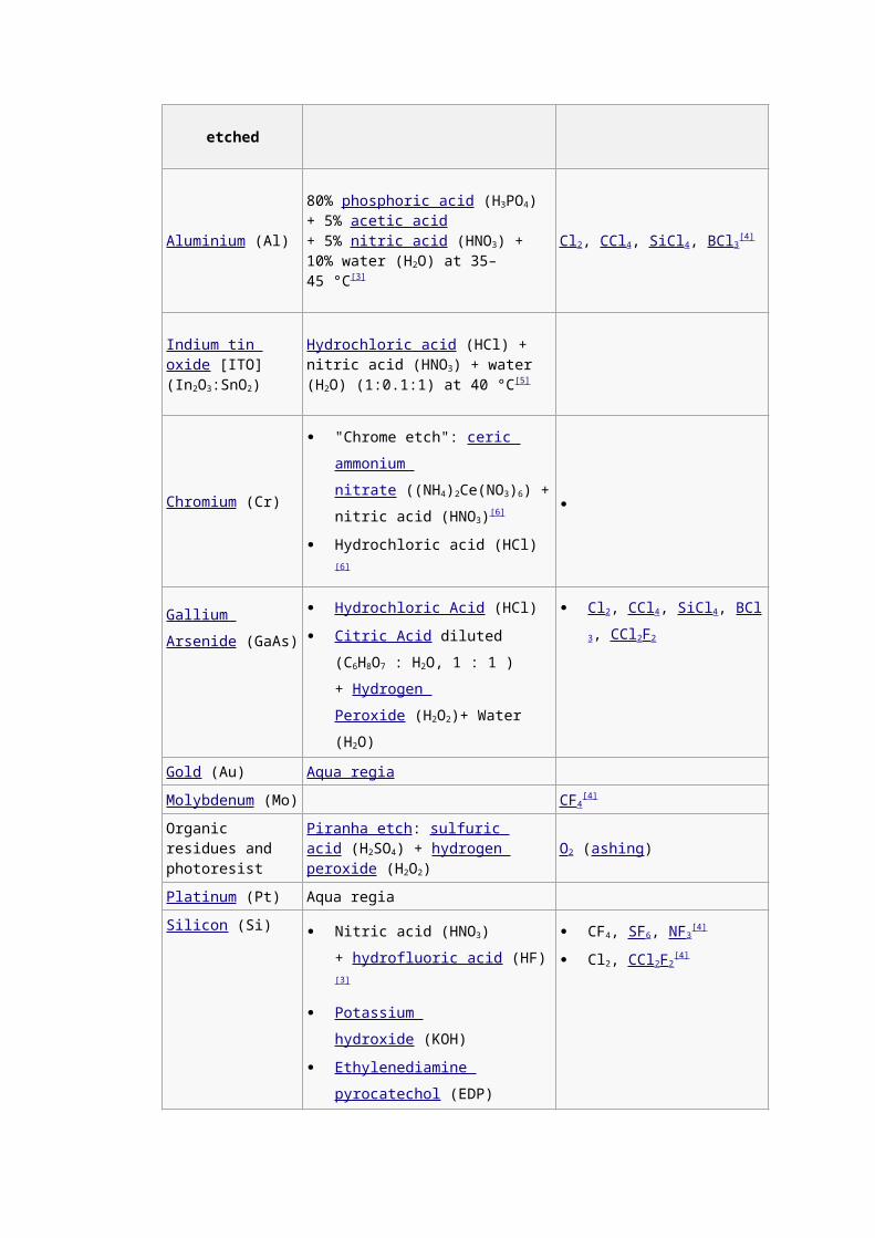
1 : 1 ) + Hydrogen Peroxide (H2O2)+
Water (H2O)
Gold (Au) Aqua regia
Molybdenum (Mo) CF4[4]
Organic residues and photoresist
Piranha etch: sulfuric acid (H2SO4) + hydrogen peroxide (H2O2)
O2 (ashing)
Platinum (Pt) Aqua regia
Silicon (Si)
Nitric acid (HNO3) + hydrofluoric
acid (HF)[3]
Potassium hydroxide (KOH)
Ethylenediamine
pyrocatechol (EDP)
Tetramethylammonium
hydroxide (TMAH)
CF4, SF6, NF3[4]
Cl2, CCl2F2[4]
Silicon dioxide (SiO2)
Hydrofluoric acid (HF)[3]
Buffered oxide
etch [BOE]: ammonium
fluoride (NH4F) and hydrofluoric
acid (HF)[3]
CF4, SF6, NF3[4]
Silicon nitride (Si3N4) 85% Phosphoric acid (H3PO4) at
180 °C[3] (Requires SiO2 etch mask)CF4, SF6, NF3,[4] CHF3
Tantalum (Ta) CF4[4]
Titanium (Ti) Hydrofluoric acid (HF)[3] BCl3[7]
Titanium nitride (TiN)
Nitric acid (HNO3) + hydrofluoric
acid (HF)
SC1
Buffered HF (bHF)
Tungsten (W)
Nitric acid (HNO3) + hydrofluoric
acid (HF)
Hydrogen Peroxide (H2O2)
CF 4[4]
SF 6[citation needed]
[edit]See also
Chemical-Mechanical Polishing
Ingot sawing
[edit]References

Jaeger, Richard C. (2002). "Lithography". Introduction to Microelectronic Fabrication (2nd
ed.). Upper Saddle River: Prentice Hall. ISBN 0-201-44494-1.
Ibid, "Processes for MicroElectroMechanical Systems (MEMS)"
[edit]Inline references
1. ̂ Finne, R.M.; Klein, D.L. (1967). "A Water-Amine-Complexing Agent System for Etching
Silicon". Journal of the Electrochemical Society 114: 965–70.
2. ̂ Shikida, M.; Sato, K.; Tokoro, K.; Uchikawa, D. (2000). "Surface morphology of
anisotropically etched single-crystal silicon". Journal of Micromechanical Microengineering 10:
522.
3. ^ a b c d e f Wolf, S.; R.N. Tauber (1986). Silicon Processing for the VLSI Era: Volume 1 -
Process Technology. Lattice Press. pp. 531–534. ISBN 0-961672-3-7.
4. ^ a b c d e f g h Wolf, S.; R.N. Tauber (1986). Silicon Processing for the VLSI Era: Volume 1 -
Process Technology. Lattice Press. p. 546. ISBN 0-961672-3-7.
5. ̂ Bahadur, Birendra (1990). Liquid Crystals: Applications and Uses vol.1. World Scientific.
p. 183. ISBN 981-02-2975-5.
6. ^ a b Walker, Perrin; William H. Tarn (1991). CRC Handbook of Metal Etchants. pp. 287–
291. ISBN 0-8493-3623-6.
7. ̂ Kohler, Michael (1999). Etching in Microsystem Technology. John Wiley & Son Ltd.
p. 329. ISBN 3-527-29561-5.
[edit]External links