Embed Size (px)
Citation preview

Department of Computer Engineering
College of Engineering
An-Najah National University
Smart Digital Pen
Prepared by :
Saif Marwan & Osama Nabulsi
Supervisor Name:
Dr. Loay Malhis
Academic Year:
2011 – 2012
1 | P a g e

Contents List
Abstraction …………………………………………………………. 4
1 Introduction …………………………………………………….. 51.1 Overview ……………………………………………………... 51.2 Existing Problems ………………………………………….... 51.3 Related Work ………………………………………………... 61.4 Motivation for Carrying out the Project ……………………6 1.5 Report Organization …………………………………………6
2 Methodology ……………………………………………………. 82.1 Building basic circuit for PIC18F4620 …………………….. 82.2 Building circuit for IR-Sensitive Camera …………………. 92.3 Create IR pen (IR Light Source) ……………....................... 132.4 Preparing SD Card and its circuit …………………………. 142.5 Preparing XBee wireless device and its configuration ……. 172.6 Programming parts ………………………………………….. 19
3 Results and Discussion …………………………………………. 254 Conclusions and Recommendations …………………………… 30
4.1 Conclusions ……………………………………………………304.2 Recommendations …………………………………………….31
5 References ……………………………………………………….. 326 Appendix ………………………………………………………… 33
2 | P a g e

List of FiguresFig.1 Basic circuit for PIC18F4620 ………………..………………………………………… 8
Fig.2 The PixArt IC Pin Assignment …………….………………………………………….. 10
Fig.3 How PixArt Camera looks …………………………………………………………..... 10
Fig.4 Wii Remote IR-sensor camera Test Circuit …………...……………………………….. 11
Fig.5 Photo of the actual circuit assembly for the IR-sensor camera ..……………………… 12
Fig.6 The shifter schematic circuit …..………………………………………………………. 13
Fig.7 IR-Pen Schematic ………………………………………………………………………. 13
Fig.8 IR Pen in real view …………..…………………………………………………………. 14
Fig.9 SD Card Pin-Outs …………………...………………………………………………….. 14
Fig.10 SD Card holder ………………………………….……………………………………. 15
Fig.11 Building Circuit for SD Card holder ………..………………………………………... 16
Fig.12 XBee Wireless device …………..…………………………………………………….. 17
Fig.13 XBee and XBee PRO Wireless devices ………………………...…………………….. 18
Fig.14 Pin configuration of XBee Series 1 802.15.4 and XBee pro. ..……………………….. 18
Fig.15 PixArt Camera footprint ….....……………………………………………………….. 27
Fig.16 IR-Sensitive Camera as a standalone device ………...……………………………….. 27
Fig.17 The Detailed System Block Diagram …….……………………………………….. 30
List of TablesTable 1 Pin-outs of the IR-Sensitive Camera …………………………………………….….. 11
Table 2 Sensitivity Blocks (1 and 2) …..……………………………………………………… 26
Table 3 Extended Mode Data Format ………………………………………………………… 26
3 | P a g e

Abstract
The development of digital pens is comparable to the invention of email. This technology has just as much potential to revolutionize the way we share information and conduct business. Some businesses have been using the electronically-enabled pens for mapping, surveying, filling out forms, and other business functions for the last few years, but consumers are just scratching the surface in understanding the multi-purpose functionality of these pens right now. Expect big developments in this technology in the next few years.
A digital pen is an input device which captures the handwriting or brush strokes of a user, converts handwritten analog information created using "pen and paper" into digital data, enabling the data to be utilized in various applications. For example, the writing data can be digitized and uploaded to a computer and displayed on its monitor. The data can then be interpreted by handwriting software and used in different applications or just as graphics.
Digital Pen captures what you write. So that you can see exactly what you're doing, a digital pen also has a conventional refill that leaves an ink trail, just like a normal pen. The ink trail is purely for your convenience: the computer doesn't "see" it or use it in any way. Every so often, you need to upload your writing to your computer.
In this documentation we will discuss all procedures that describe how we built a Smart Digital Pen by using special IR-Sensitive Camera that detect IR LED which is built inside pen itself.
4 | P a g e

1. Introduction
1.1 Overview
Today, time frames are shorter than ever. The focus is on faster, more accurate and more efficient processes—which lead to improved results. Managing information in handwritten forms and hard-copy documents remains an essential task for many businesses and institutions, but is often a slow, inefficient process. In fact, a recent study from Anoto found that 86% of companies are still using paper-based forms for business data capture.
In order to improve the way businesses currently capture handwritten information, there are many ideas to provide the Digital Pen Printing Solution, which allows you to transfer handwritten notations into the original electronic document and save it .
Electronic pens are useful for college students, journalists and business people. Many pens are marketed for use in the educational environment, but Live scribe, manufacturer of the Smart pen, says that 70 percent of their customer base uses the computerized pens for business-related purposes. The pens are also fun for children.
The main objective of this project is to make a sample of smart digital pen, which describe the same functionality of the original digital pen that are marketed in the world, but by using available simple tools.
1.2 Existing Problems
Most of old versions of digital pens use a special paper in order to keep tracking for the position of head of the pen. But in our project, we can use that digital pen at any ordinary paper and also at any tools for writing in the region which the camera can detect it.
5 | P a g e

By using the new versions of digital pens, although we don't need a special paper but these digital pens use special sensors and complicated circuits, are built inside them. By the way, in our project we used simple available tools, to build our smart digital pen.
As a result, our application with its features came to provide the same targets and functionality of the original digital pen, and also we can use it in different ways.
1.3 Related Work
As we said above, there are many companies build and create digital pens and always trying to develop a lot of features for that products.
But products like digital pens need more specific and accurately tools, and it is great to build tools with the same functionality and features outside special factories and without special microcontrollers.
1.4 Motivation for Carrying out the Project
This is our Graduation Project, so we hope to carry out our project in best possible condition, in order to do something express our gratitude to our university and enhance the confidence of our doctors and teachers and make them proud of us.
Also, supervisors always follow up and encourage us, and this is another reason to work on project’s success.
1.5 Report Organization
This document discuss the functionality of our project included the features in each part of it. In addition, we will summarize all the results that we got it in this project.
6 | P a g e

We will find that in our document, contents for each section as follow :
Methodology Section : we will describe the methods used to establish facts and ideas for this project.
Results and Discussion Section : we will turn to discuss the parts of creating the “Smart Digital Pen” step by step, include problems which we met them, and how we solved these problems to get the best outputs possible. Conclusions and Recommendations section : we will find our recommendations and conclusions about this project, and how we can develop this product in order to use it commonly in different working life.
7 | P a g e

2. Methodology
The steps that were carried out for implementing the project are :
Building basic circuit for PIC18F4620. Building circuit for IR-Sensitive Camera. Create IR pen (IR Light Source). Preparing SD Card and its circuit. Preparing XBee wireless device and its configuration. Programming parts.
2.1 Building basic circuit for PIC18F4620 :
At the first step of our graduation project which used PIC18F4620, we built basic circuit for that PIC in order to use it as a basic part in any applications implement by PIC devices.
And we built this basic circuit as the following :
Fig.1 Basic circuit for PIC18F4620
8 | P a g e

2.2 Building circuit for IR-Sensitive Camera:
This is the most important part in our project, we use PixArt CMOS sensor consists of two functional parts:
1. The actual sensing part, were up to four IR points can be detected at the same time.
2. The internal processor part, which is responsible of translating the location of the IR points to correct x,y coordinates and size value (which gives a parameter indicating the distance of the IR point from the cameras position).
Other Specifications:
• 8 pins (4x2)
• Operates with 3.3V.
• 25 MHz clock.
• I²C (Inter-Integrated Circuit) Bus communication. (400 KHz fast with slave address 0xB0).
• Field of View is about 33 degrees horizontally and 23 degrees vertically.
• 3 sensitivity modes.
Since this chip evolved from the incorporation of two companies (Nintendo and PixArt) there is no public datasheet, all the information gathered are from various engineering researches and individual contributions.
Initialization and Sensitivity Modes :
The chip must be enabled by certain instruction formats, which will leave it in one of three states:
1. On, but no data is being taken.
2. On, and data is being taken at half sensitivity.
3. On, and data is being taken at full sensitivity.
9 | P a g e

The data output format will differ according to these states, but can still be categorized in three modes:
1. Basic. (10 bytes , 5 bytes for each pair, with a total of 4 dots “two pairs”)
2. Extended. (12 bytes, 3 bytes for each dot, with a total of 4 dots)
3. Full. (36 bytes, 9 bytes for each dot, with a total of 4 dots)
The main difference between each mode is the number of bytes being transmitted for each IR dot, and whether the rough size value for each dot is required or not (We used the extended mode for our approach).
The Pin assignment and the actual packaging for the camera chip:
Fig.2 The PixArt IC Pin Assignment
And the following figure describes how the PixArt Camera looks like, after we got it from original Wii Mote device.
Fig.3 How PixArt Camera looks
10 | P a g e

Pin-outs:
Pin # Description1 pulled up to +3.3 V
2 , 3 Grounded4 not connected5 Serial Clock. (I²C Bus)6 Serial Data Line. (I²C Bus)7 Components clock. (25 MHz)8 Active low Reset (can be pulled up to
Vcc)
Table 1 Pin-outs of the IR-Sensitive Camera
Another note before jumping to the next section, is that the communication with the camera chip will be through I²C bus protocol, which is a master/slave architecture were all devices are connected together by two signals : serial clock (SCL) (Pin 5) and serial data (SDA) (Pin 6).
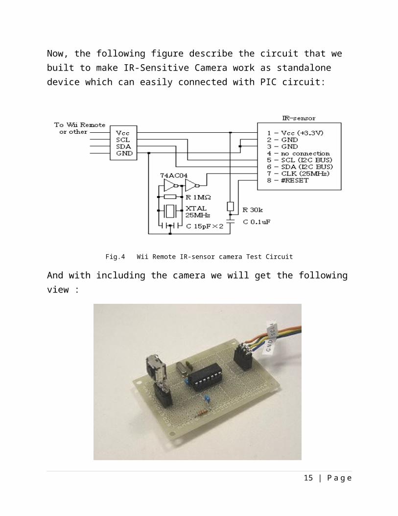
Now, the following figure describe the circuit that we built to make IR-Sensitive Camera work as standalone device which can easily connected with PIC circuit:
Fig.4 Wii Remote IR-sensor camera Test Circuit
11 | P a g e

And with including the camera we will get the following view :
Fig.5 Photo of the actual circuit assembly for the IR-sensor camera
But here we met a problem that voltage level difference between the PIC and the IR-Camera, since the first operates correctly at 5V and the camera at 3.3V. Both the SDA and SCL lines from both sides should be pulled up to Vdd, but since we have two levels (5V and 3.3V) we decided to pull them up to 3.3V; since the IR-Camera’s pins are not tolerant to 5 volts.
So, to solve this problem we built a bi-directional level shifter N-Channel MOSFET circuit between the PIC (5V device) and the Camera (3.3V device) as recommended by PHILLIPS (which by the way established the protocols of I²C communication).
12 | P a g e

Fig.6 The shifter schematic circuit
2.3 Create IR pen (IR Light Source) :
An IR LED is the simplest way for generating a reasonable IR light source; of course this LED is attached to a regular pen and triggered via a momentary switch button for an easier usage.
Fig.7 IR-Pen Schematic
13 | P a g e

And in the real view, we got the following pen built with IR circuit together :
Fig.8 IR Pen in real view
2.4 Preparing SD Card and its circuit :
SD Cards (Secure Digital Cards) are quite popular these days for things like digital camera's, video camera's, mp3 players and mobile phones. Now we will have one in our project ! The main advantages are: small size, large data storage capability, speed, cost. It has flash storage that does not require power to hold data.
SD Card has 2 data transfer types "SD Bus" and "SPI Bus". Most PIC's have an SPI port. The "SD Bus" is faster, however uses more pins. We will be using SPI in our circuit.
Fig.9 SD Card Pin-Outs
14 | P a g e
These SD Cards are 3.3v devices, therefore a 5v to 3v conversion is needed between the PIC and the SD card. We will use resistors to do the conversion, however there are many other methods.
Build a SD Card Slot :
Before we can build our circuit, we will need to find an SD card slot that can plug into our breadboard. We took one out of a broken digital camera and placed it on some blank breadboard and soldered on some pins. Here are some images of my SD card holder:
Fig.10 SD Card holder
15 | P a g e

Build the circuit :
Follow this schematic for PIC18F4620, check the pin-outs for the SPI bus. The pin-outs of our PIC will show SDI, SDO, SCL and SS. The pin SS is the chip select pin, we can use any pin for it but the others must stay the same.
Fig.11 Building Circuit for SD Card holder
16 | P a g e

2.5 Preparing XBee wireless device and its configuration :
XBee is a wireless communication device that uses ZigBee protocol. ZigBee is a specification for a suite of high level communication protocols using small, low-power digital radios based on the IEEE 802.15.4 standard for wireless personal area networks (WPANs), such as wireless headphones connecting with cell phones via short-range radio. The technology defined by the ZigBee specification is intended to be simpler and less expensive than other WPANs, such as Bluetooth. ZigBee is targeted at radio-frequency (RF) applications that require a low data rate, long battery life, and secure networking.
Fig.12 XBee Wireless device
It operates with 3.3V and uses 50mA. Some XBee's pins can be set as Analog Input, Digital Input, Digital Output, or Analog Output (PWM). The numbers of pins are up to seven channels of analog input, nine channels of digital I/O and two channels of PWM. This means we do not need microcontroller to send sensor input to our computer.
In the same way, XBee and XBee-PRO 802.15.4 OEM RF modules are embedded solutions providing wireless end-point connectivity to devices. These modules use also the IEEE 802.15.4 networking protocol for fast point-to-multipoint or peer-to-peer networking. They are designed for high-throughput applications requiring low latency and predictable communication timing.
17 | P a g e

Fig.13 XBee and XBee PRO Wireless devices
These devices have the following characteristics:
No configuration needed for out-of-the-box RF communications. Common XBee footprint for a variety of RF modules. Fast 250 kbps RF data rate to the end node. 2.4 GHz for worldwide deployment. Sleep modes supported for extended battery life.
Fig.14 Pin configuration of XBee Series 1 802.15.4 and XBee pro.
18 | P a g e

2.6 Programming parts :
Theory of Operation:
• The PIC (master device) issues a start condition, hence the camera chip (slave) starts listening on the serial line to see if it is the one concerned (by checking the address sent by the master and comparing it with its own)
• A read/write operation is specified accordingly by the PIC (master)
• The PIC (master) starts transmitting and waits for an acknowledgement from the camera chip (slave). Usually the transmitter sends 8-bits of data and the receiver replies with a one bit ACK (I²C standards).
• The PIC (master) issues a stop condition when the communication is complete.
This operation is valid when the PIC is issuing a write command (hence sending instructions to initialize the camera), or when it is issuing a read command (when it is reading the data coordinates form the camera).
After filling the data buffers with the x, y coordinates, they get directed from the D+, D- pins of the PIC to the enablement software on the PC host through a USB connector.
PixArt IR-Camera Interfacing :
The original Bread Board was modified with this design and the whole board was tested for the following:
• Send the camera’s initialization sequence and wait for an ACK from the camera.
• Build C-code by defining a READ-IR command on the PIC side that is triggered by a C# application on the PC side, and send the result for further visual testing to the PC side.
The result at this stage was three integers representing x,y coordinates and the blob size (s), in the following order:
• If no IR source is present x = 0, y = 0, s = 0
• Else one of the three values would be not equal to zero
19 | P a g e

The second test was more on the PC-side (C# application), were the program was set to send an IR-READ request on an interval of 300 ms (done by setting a counter with an interval of 300) and the x,y result was used to move a red circle on a black background, which seemed as a visual representation of the IR light source on the move, hence it would act and change position in the same manner as we apply an action on the IR source.
This proved that the x,y coordinates obtained are not noise signals, but on the contrary they present valid and correct IR source position based on the camera’s field of view.
This program prototype is used for debugging reasons, in order to find out the camera’s FOV on a certain surface and at a specific distance.
The hardware part to this stage was stable, and the work now was to be shifted to the Enablement software part, before combining the two.
SD Card Software :
With the use of the SD card lib (sd_card.jal) and a sample file 18f4620a_sd_card.jal, we can easily put one in our own circuit for mass data storage! we will find these files in the lib & sample directories of our jallib installation.
Now compile and program pic with 18f4620a_sd_card.jal from our jallib samples directory.
Then we have compiled it, burn the .hex file to our PIC.
Understand and modify the code :
We are just going to quickly go over some of the key points we need to know about SD cards. Open the sample file with an editor if you have not done so already.
The code in the sample file may change, therefore it may be different then what we see here. The sample file we have downloaded will always be tested and correct.
20 | P a g e

Include the chip
Specify the PIC we wish to use as well as our clock frequency
include 18f4620a
--
pragma target OSC HS -- HS crystal or resonator
pragma target clock 20_000_000 -- oscillator frequency
--
pragma target WDT disabled
pragma target LVP disabled
Disable all analog pins and wait for power to stabilize
enable_digital_io() -- disable all analog pins if any
_usec_delay (100_000) -- wait for power to stabilize
Setup serial port and choose baud rate 115200
-- setup part for communication
const serial_hw_baudrate = 115200 -- set the baud rate
include serial_hardware
serial_hw_init()
21 | P a g e

Include the print library
include print -- include the print library
Setup SPI Settings - The data transfer bus.
Here we may change the chip select pin "pin_SS" and "pin_SS_direction" to another pin. SDI, SDO and SCK must stay the same for the SPI hardware library.
We may notice that we are not defining/aliasing pins sdi, sdo and sck. We do not need to define them with a line like "alias pin_sdo is pin_c5" because they are set within the PIC and cannot be changed. If we use the SPI hardware library, we must use the SPI hardware pins. We only need to define their direction like this "pin_sdo_direction = output".
We may also choose the SPI rate. According to the SPI hardware library, we can use SPI_RATE_FOSC_4 SPI_RATE_FOSC_16, SPI_RATE_FOSC_64 or SPI_RATE_TMR. The fastest is FOSC_4 (oscillator frequency / 4). For the fastest speeds, it is a good idea to keep your SD Card as close to the PIC as possible.
include spi_master_hw -- includes the spi library
-- define spi inputs/outputs
pin_sdi_direction = input -- spi input
pin_sdo_direction = output -- spi output
pin_sck_direction = output -- spi clock
--
22 | P a g e

spi_init(SPI_MODE_11,SPI_RATE_FOSC_4) -- init spi, choose mode and speed
alias sd_chip_select is pin_a5
alias sd_chip_select_direction is pin_a5_direction
sd_chip_select_direction = output
Setup the SD Card library and settings
Select SD card settings & Include the library file, then initialize the SD card.
Some SD cards may require a 10ms (or more) delay every time you stop writing to the SD card, we can choose whether or not to have this delay. If we are doing many small writes and are worried about speed, we may set SD_DELAY_AFTER_WRITE to "FALSE".
-- setup the sd card
const bit SD_ALWAYS_SET_SPI_MODE = TRUE
const bit SD_DELAY_AFTER_WRITE = TRUE
include sd_card -- include the sd card idle hard disk library
sd_init() -- initialize startup settings
-- procedure for sending 80 "-----------------" via serial port
procedure seperator() is
serial_hw_data = 13
serial_hw_data = 10
const byte str3[] = "--------------------------------------------------------------------------------"
print_string(serial_hw_data, str3)
23 | P a g e

print_crlf(serial_hw_data)
end procedure
It is always a good idea to send something to the serial port so we know the circuit is alive. Let's send "Hard Disk Sample Started"
-- Send something to the serial port
seperator() -- send "----" via serial port
var byte start_string[] = "SD CARD SAMPLE STARTED"
print_string(serial_hw_data,start_string)
Declare some user variables
-- variables for the sample
var word step1
var byte data
C# Application Software :
Finally, we implemented simple C# application program in order to see output coordinates that sent by IR Pen and convert them to meaningful data.
So, we created an application that reads these data coordinates and draws point for each coordinate, and all these points will create for us digital handwriting.
In addition, this application has some features that allows for user to do some editing on the handwriting output.
24 | P a g e

3. Results and Discussion By this section, we will discuss briefly about our demo for this project.
All the communication taking place at this stage is over the SDA line of the I²C bus, were the PIC Microcontroller acts as the master and the camera chip acts as the only slave connected to the bus lines (SCL,SDA).
In order to make the interface compatible as possible with the modern PIC compilers, dynamic link libraries, and port drivers we decided to clone the schematics of this commercial board and produce our home-made copy with the essential hardware parts needed to achieve our communication and initialization goals.
What are the advantages of doing this?
• Making use of the C#.NET classes that were developed by Microchip to establish basic send receive commands/data between the PC and PIC.
• Using the Microchip-supplied driver mpusbapi.dll which enables the PC to define the board as a USB device that it can later relate to.
• Enabling the hardware developer to use vast Microchip middleware’s, Boot-loaders, debuggers and already existing examples whether on the PC side or on the PIC side.
Initialization and Sensitivity Modes :
Send 0x04 to Output Report 0x13
Send 0x04 to Output Report 0x1a
Write 0x08 to register 0xb00030
Write Sensitivity Block 1 to registers at 0xb00000
Write Sensitivity Block 2 to registers at 0xb0001a
25 | P a g e

Write Mode Number to register 0xb00033 (Mode number: basic =1, extended =3, full =5)
Write 0x08 to register 0xb00030 (again)
Block1 Block200 00 00 00 00 00 90 00 c0 40 0002 00 00 71 01 00 aa 00 64 63 0300 00 00 00 00 00 90 00 41 40 0002 00 00 71 01 00 64 00 fe fd 0502 00 00 71 01 00 96 00 b4 b3 0402 00 00 71 01 00 aa 00 64 63 0302 00 00 71 01 00 c8 00 36 35 0302 00 00 71 01 00 72 00 20 1f 03
Table 2 Sensitivity Blocks (1 and 2)
Data Output Formats from the IR-Camera Extended Mode :
BitByte 7 6 5 4 3 2 1 0
0 X[7:0]1 Y[7:0]2 Y[9:8] X[9:8] S[3:0]
Table 3 Extended Mode Data Format
Now, we will convert to talk about problems and difficulties that we met during our works in this project, and how we dealt with them.
26 | P a g e

Difficulties of Hardware development :
Problem: IR-Camera’s pins are hard to plug in the holes of a regular breadboard (pins are small and too close); since the IC itself doesn’t follow the typical DIP pins that are usually used for breadboard prototyping.
Fig.15 PixArt Camera footprint
Solution: solder the pins with the tip of a thin serial cable, and attach connectors to the other side, to sit correctly on the breadboard, and finally welded these wires to pins socket in order to make it fixed as a standalone device, and flexible to move in and out from the circuit.
Fig.16 IR-Sensitive Camera as a standalone device
27 | P a g e

Problem: the SDA lines keep reading 0xFF (“255” a permanent logic high) from the pins of the IR-Camera.
Problem diagnoses: voltage level difference between the PIC and the IR-Camera, since the first operates correctly at 5V and the camera at 3.3V. Both the SDA and SCL lines from both sides should be pulled up to Vdd, but since we have two levels (5V and 3.3V) we decided to pull them up to 3.3V; since the IR-Camera’s pins are not tolerant to 5 volts.
Initial Solution: change the standard I²C pull-up resistors from 4.7K to 1.5 K.
Result: SDA lines keeps reading 0xFF
Final solution: built a bi-directional level shifter N-Channel MOSFET circuit between the PIC (5V device) and the Camera (3.3V device) as recommended by PHILLIPS (which by the way established the protocols of I²C communication).
Problem: stops sending data (freezes) after working for 2-3 minutes.
Problem diagnoses: I²C slave (IR-Camera) locks the I²C bus after sending the data, hence the master (PIC) can’t get the upper hand and keeps looping endlessly.
Solution: made sure that the slave left the bus by sending a negative acknowledgement form the master’s side telling it that no more data is needed for this round of sampling.
Last two lines of the reading routine:
SendNack();
SendStop();
28 | P a g e

Problem: first full system demo wasn’t satisfying since the sampling rate was too slow to cope with the IR stimulus.
Initial problem diagnoses: the translation of the spatial coordinates to actual screen sized coordinates (a matrix multiplication operation) is taking a long time at the PC-side.
Initial solution: migrating few mathematical processes to the PIC’s-side and optimizing the translation operation.
Result: problem wasn’t solved.
Secondary solution: changed the usb endpoint time interval from 32-ms to 1-ms reporting in the usb descriptor header file (usbdsc.h).
Result: the performance of the sampling rate definition improved, but still wasn’t perfect.
Final solution: changed the logic used for emulating the IR stimulus.
29 | P a g e

4. Conclusions and Recommendations
4.1 Conclusions
The Digital Pen Printing Solution allows you to:
Make information available quickly and easily Boost operational efficiencies Reduce costly errors Aid in compliance Free up valuable resources
By this project, we created a model from the smart digital pen that simulates the basic functions for original one.
So, IR-Camera captures movement of IR-LED Pen and transfers these to PC, in which the enablement software utilizes the movement toward drawing points with X-Y coordinates relative to surface`s borders, then can that digital handwriting used for interactive applications.
On the other hand, The Input of the system is the IR-light emitted from the customized IR-PEN, this light is detected by the IR-Sensing unit (in PixArt Camera) and is later converted by the internal processor of the camera to equivalent x,y coordinates, which are passed to the PIC microcontroller and from there to the PC for additional processing to create digital handwriting behavior.
Fig.17 The Detailed System Block Diagram
30 | P a g e

Finally, we used XBee wireless device as an additional feature to our project, which by using this feature we can make synchronization between IR-Pen and our C# application. In other world, by using XBee wireless and it's configuration with our project, we can easily writing by IR-Pen and see the result directly in our C# application, and get traditional copy by ordinary paper, and digital copy by our project at the same time.
4.2 Recommendations
Digital pens will likely be a social revolution. Technology today provides for electronic writing devices that are comparable to the regular ink pens we are so familiar with. Handwriting in digital form allows for quick and convenient transmittal of messages to friends and colleagues.
In our project, we recommend to complete our implementation for the SD card with our project, in order to add more huge storage for PIC memory, that allows for storing more and more data when we use this project as portable project.
Also, we looking forward to develop our software application to make it able to edit the output digital handwriting as any documents application, more than editing we achieved. So, this make that project more user friendly and can fix any mistakes that may be done during handwriting.
By few words we can say that:
• There are many creative ideas that can be implemented in the system even after finishing the project as graduation project; this gives the Smart Digital Pen the real opportunity to be commercial product later because it offers low cost solutions for educational centers in Arab world.
• Beside Education, software can be developed to benefit from the hardware to form a platform of usage in other fields as business, meeting, and marketing.
• Testing is more powerful than traditional debugging mode, because it is not only used to locate defects and correct them it also offers validation and reliability measurement.
31 | P a g e

5. References
http://translate.google.com/translate?u=http%3A%2F%2Fwww.kako.com%2Fneta%2F2007-001%2F2007-001.html&hl=en&ie=UTF-8&sl=ja&tl=en
http://www.instructables.com/id/Wii-Remote-IR-Camera-Hack/ http://www.explainthatstuff.com/digitalpens.html http://digital-pen-review.toptenreviews.com/ http://www.okidata.com/mkt/html/nf/PS_Digital-Pen-Overview.html http://justanotherlanguage.org/book/export/html/151 http://wiibrew.org/wiki/Wiimote http://www.digi.com/products/wireless-wired-embedded-solutions/zigbee-rf-
modules/point-multipoint-rfmodules/xbee-series1-module#overview http://www.kobakant.at/DIY/?p=1215 http://www.libelium.com/squidbee/index.php?
title=How_to_set_XBee_parameters
32 | P a g e

6. Appendix
All materials and instruments including programming and software part, also all hardware devices that we used to build our project, you can find them by our graduation project demo "Smart Digital Pen".
33 | P a g e


![OpenMP - IPSltodi.est.ips.pt/aabreu/openMP.pdf · #pragma omp sections [clause ...] newline {#pragma omp section newline structured_block #pragma omp section newline structured_block}](https://img.pdfslide.us/doc/110x75/5e752997f76299646930422c/openmp-pragma-omp-sections-clause-newline-pragma-omp-section-newline.jpg)