Embed Size (px)
Citation preview
Contents:
Chapter1 : Introduction1.1 Bridge Characteristics…………………………………..……………………1
1.2 The idea of the project…………………………………………………..…...2
1.3 Mathematical analysis………………………………………………….….…3
Chapter2: Triggering the thyristor 2.1 Thyristor turn on and I-V Characteristics…………..……………….…..…6
2.2 Thyristor Triggering Circuit……………………………………………..…112.3 Zero Crossing Detector Triggering Circuit…………………………………….…15
Chapter 3 : Building the Bridge 3.1 Thyristor (TIC 116) ……………..…………………………………….…..…25
3.2 The circuit operation………………………………………………….…...…26
3.3 Triggering transportation……………………………………………………28
3.4 The complete circuit of the project…………………………………….…….34
Chapter 4 : Investigation about the input and output characteristics4.1 investigation input and output characteristics of pure resistive load……...46
4.2 investigation input and output characteristics of R-L load……………..…50
4.3 DC motor speed control……..……………………………………………...…63
4.4 investigation about the improvement of the grid current……………...……67
Chapter 5: Discussion and conclusion………………………………………………………….…73
I
LIST OF FIGURES
FIGURE 1: THE SINGLE PHASE BRIDGE RECTIFIER......................................4FIGURE 2: SINGLE PHASE UPS.....................................................................4FIGURE 3: THE WAVE FORMS FOR CONTINUOUS OPERATIONS:...................6FIGURE 4: THYRISTOR CONSTRUCTION.......................................................9FIGURE 5: LAYER DIAGRAM OF THYRISTOR.............................................10FIGURE 6: IV- CHARACTERISTICS.............................................................12FIGURE 7: ASTABLE MULTIVIBRATOR CIRCUIT DIAGRAM USING THE 555
TIMER.................................................................................................14FIGURE 8: MONOSTABLE MULTIVIBRATOR CIRCUIT DIAGRAM USING THE
555 TIMER..........................................................................................15FIGURE 9: UNIJUNCTION TRANSISTOR RELAXATION OSCILLATOR AND
WAVEFORMS. OSCILLATOR DRIVES SCR............................................16FIGURE 10: PULSE TRANSFORMER............................................................17FIGURE 11: ZERO CROSS DETECTOR TRIGGERING CIRCUIT.......................18FIGURE 12: INPUT VOLTAGE OF ZERO CROSS DETECTION........................20FIGURE 13: OUTPUT VOLTAGE OF ZERO CROSS DETECTION....................20FIGURE 14: PIC CHIP................................................................................21FIGURE 15: PIC BASIC CIRCUIT................................................................22FIGURE 16: PRINTED CIRCUIT BOARD OF THE PIC BASIC CIRCUIT............23FIGURE 17: FLOW CHART FOR TRIGGERING THYRISTOR...........................24FIGURE 18: TRIGGERING AT 0°.................................................................26FIGURE 19: TRIGGERING AT 30°...............................................................26FIGURE 20: TRIGGERING AT 45°...............................................................27FIGURE 21: TRIGGERING AT 90°...............................................................27FIGURE 22: TRIGGERING AT 120°.............................................................27FIGURE 23: TYRISTOR TIC 116................................................................28FIGURE 24: DIRECT CONNECTION BETWEEN THE PIC AND THE BRIDGE..32FIGURE 25: TRIAC PHOTO COUPLER (MOS 3020).....................................32FIGURE 26: MAKE CONNECTION BETWEEN PIC AND BRIDGE BY USING
MOS 3020..........................................................................................34FIGURE 27: MAKE CONNECTION BETWEEN PIC AND BRIDGE BY USING
PHOTO COUPLER BETWEEN ANODE AND GATE....................................34FIGURE 28: TRANSISTOR PHOTO ISOLATOR (4N25)...................................35FIGURE 29: MAKE CONNECTION BETWEEN PIC AND BRIDGE BY USING
TRANSISTOR PHOTO ISOLATOR (4N25)................................................36
II
FIGURE 30: THE COMPLETE CIRCUIT OF THE PROJECT..............................37FIGURE 31: PRINTED CIRCUIT BOARD OF COMPLETE CIRCUIT...................39FIGURE 32: OUTPUT VOLTAGE FORM AT R=16, Α = ZERO°......................50FIGURE 33: OUTPUT VOLTAGE FORM AT R=16, Α = 45°..........................50FIGURE 34: OUTPUT VOLTAGE FORM AT R=16, Α = 90°..........................50FIGURE 35: OUTPUT VOLTAGE FORM AT R=16, Α = 135°........................51FIGURE 36: INPUT CURRENT FORM AT R=16, Α = ZERO°.........................51FIGURE 37: INPUT CURRENT FORM AT R=16, Α = 45°.............................52FIGURE 38: INPUT CURRENT FORM AT R=16, Α = 90°.............................52FIGURE 39: INPUT CURRENT FORM AT R=16, Α = 135°...........................52FIGURE 40: OUTPUT VOLTAGE FORM AT Ф= 53.9°, Α = ZERO°................53FIGURE 41: OUTPUT VOLTAGE FORM AT Ф= 53.9°, Α = 45°....................54FIGURE 42: OUTPUT VOLTAGE FORM AT Ф= 53.9°, Α = 90°....................54FIGURE 43: OUTPUT VOLTAGE FORM AT Ф= 53.9°, Α = 135°..................54FIGURE 44: INPUT CURRENT FORM AT Ф= 53.9°, Α = ZERO°...................55FIGURE 45: INPUT CURRENT FORM AT Ф= 53.9°, Α = 45°.......................55FIGURE 46: INPUT CURRENT FORM AT Ф= 53.9°, Α = 90°.......................55FIGURE 47: INPUT CURRENT FORM AT Ф= 53.9°, Α = 135°.....................56FIGURE 48: OUTPUT VOLTAGE FORM AT Ф= 74.73°, Α= ZERO°...............57FIGURE 49: OUTPUT VOLTAGE FORM AT Ф= 74.73°, Α= 45°...................57FIGURE 50: OUTPUT VOLTAGE FORM AT Ф= 74.73°, Α= 90°...................57FIGURE 51: OUTPUT VOLTAGE FORM AT Ф= 74.73°, Α= 135°.................58FIGURE 52: INPUT CURRENT FORM AT Ф= 74.73°, Α = ZERO°.................58FIGURE 53: INPUT CURRENT FORM AT Ф= 74.73°, Α = 45°.....................58FIGURE 54: INPUT CURRENT FORM AT Ф= 74.73°, Α = 90°.....................59FIGURE 55: INPUT CURRENT FORM AT Ф= 74.73°, Α = 135°...................59FIGURE 56: OUTPUT VOLTAGE FORM AT Ф= 78.06°, Α= ZERO°...............60FIGURE 57: OUTPUT VOLTAGE FORM AT Ф= 78.06°, Α= 45°...................60FIGURE 58: OUTPUT VOLTAGE FORM AT Ф= 78.06°, Α= 90°...................60FIGURE 59: OUTPUT VOLTAGE FORM AT Ф= 78.06°, Α= 135°.................61FIGURE 60: INPUT CURRENT FORM AT Ф= 78.06°, Α = ZERO°.................61FIGURE 61: INPUT CURRENT FORM AT Ф= 78.06°, Α = 45°.....................61FIGURE 62: INPUT CURRENT FORM AT Ф= 78.06°, Α = 90°.....................62FIGURE 63: INPUT CURRENT FORM AT Ф= 78.06°, Α = 135°...................62FIGURE 64: OUTPUT VOLTAGE FORM AT Ф= 83.61°, Α= ZERO°...............63FIGURE 65: OUTPUT VOLTAGE FORM AT Ф= 83.61°, Α= 45°...................63FIGURE 66: OUTPUT VOLTAGE FORM AT Ф= 83.61°, Α= 90°...................63
III
FIGURE 67: OUTPUT VOLTAGE FORM AT Ф= 83.61°, Α= 135°................64FIGURE 68: INPUT CURRENT FORM AT Ф= 83.61°, Α = ZERO°.................64FIGURE 69: INPUT CURRENT FORM AT Ф= 83.61°, Α = 45°.....................64FIGURE 70: INPUT CURRENT FORM AT Ф= 83.61°, Α = 90°.....................65FIGURE 71: INPUT CURRENT FORM AT Ф= 83.61°, Α = 135°...................65FIGURE 72: EQUIVALENT CIRCUIT OF THE DC MOTOR CONNECTED TO
THE SINGLE PHASE BRIDGE.................................................................66FIGURE 73: OUTPUT VOLTAGE OF DC MOTOR AT Α= ZERO°...................66FIGURE 74: OUTPUT VOLTAGE OF DC MOTOR AT Α= 45°........................67FIGURE 75: OUTPUT VOLTAGE OF DC MOTOR AT Α= 90°........................67FIGURE 76: OUTPUT VOLTAGE OF DC MOTOR AT Α= ZERO°...................67FIGURE 77: THE INPUT CURRENT OF DC MOTOR Α = ZERO°....................68FIGURE 78: THE INPUT CURRENT OF DC MOTOR Α =45°.........................68FIGURE 79: THE INPUT CURRENT OF DC MOTOR Α = 90°........................68FIGURE 80: THE INPUT CURRENT OF DC MOTOR Α =135°.......................69FIGURE 81: THE INPUT CURRENT WAVEFORMS AFTER FILTERING AT FC=
398 HZ................................................................................................74FIGURE 82: THE INPUT CURRENT WAVEFORMS AFTER FILTERING AT FC=
159 HZ................................................................................................74FIGURE 83: THE INPUT CURRENT WAVEFORMS AFTER FILTERING AT FC=
79 HZ..................................................................................................74FIGURE 84: THE INPUT CURRENT WAVEFORMS AFTER FILTERING AT FC=
53 HZ..................................................................................................75
IV
LIST OF TABLES
TABLE 1: IV- CHARACTERISTICS OF THYRISTOR......................................12TABLE 2: CHARACTERISTICS TRIAC PHOTO COUPLER (MOS 3020)..........34TABLE 3: CHARACTERISTICS TRANSISTOR PHOTO ISOLATOR (4N25).......36TABLE 4: VODC, IINP, AND IODC AT VINP= 20V, R= 16Ω AND DIFFERENT
FIRING ANGLES...................................................................................54TABLE 5: VODC, IINP, AND IODC AT VINP= 20V, Ф= 53.9°AND
DIFFERENT FIRING ANGLES.................................................................57TABLE 6: VODC, IINP, AND IODC AT VINP= 20V, Ф= 74.73°AND
DIFFERENT FIRING ANGLES.................................................................60TABLE 7: VODC, IINP, AND IODC AT VINP= 20V, Ф= 78.06°AND
DIFFERENT FIRING ANGLES.................................................................63TABLE 8: VODC, IINP, AND IODC AT VINP= 20V, Ф= 83.61°AND
DIFFERENT FIRING ANGLES.................................................................66TABLE 9: VALUES FOR L AND C FOR RESONANCE CIRCUIT.....................73
V
Chapter One: Introduction1.1 Bridge Characteristics:
Figure 1: The single phase bridge Rectifier
Single phase bridge rectifier has many characteristics and applications which make it widely used in the industrial applications and these characteristics can be summarized in the following points:a-.Two quadrant operation is possible.b-The thyristors are triggered at an interval of p .c-It is also used to control the speed of DC motors.d-This circuit is widely used in dual converters (ups) as battery charger.
Figure 2: Single phase ups
1

f-It can be used in continuous mode depend on the firing angle.
1.2 The idea of the project:
Is to build a single phase full controlled bridge rectifier ,use it to supply different types of load and to make investigations about the improvement of its grid current.
2
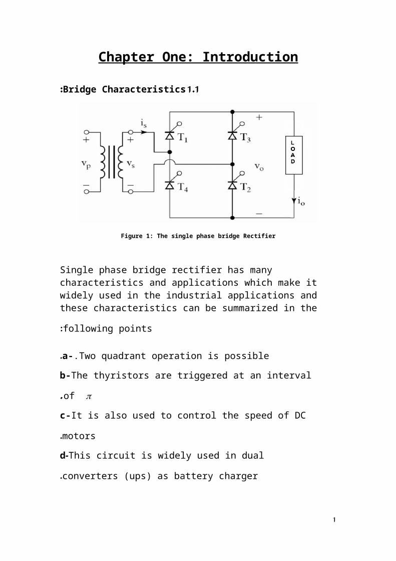
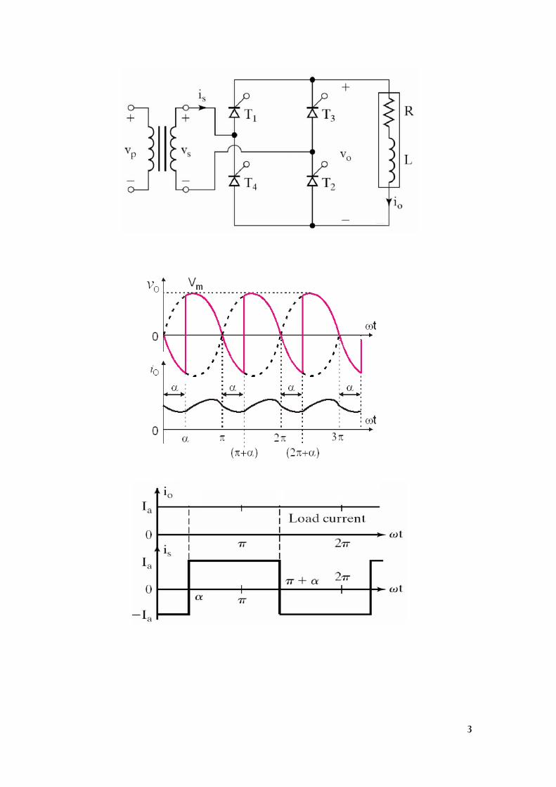
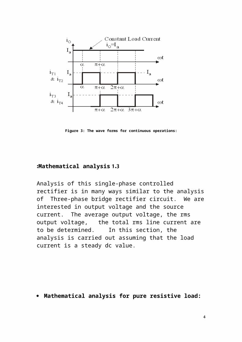
Figure 3: The wave forms for continuous operations:
1.3 Mathematical analysis:
Analysis of this single-phase controlled rectifier is in many ways similar to the analysis of Three-phase bridge rectifier circuit. We are interested in output voltage and the source current. The average output voltage, the rms output voltage, the total rms line current are to be determined. In this section, the analysis is carried out assuming that the load current is a steady dc value.
3

Mathematical analysis for pure resistive load:
Vdc= 1× 22 π ∫
0
π
Vm×sin(ωt) . dωt
Vdc =2Vmπ
Vdc=0.636Vm.
Idc =2Vmπ R
Vdrms=√ 1×22π ∫
0
π
(Vm× sin ( ωt ))2 . d ωt
Vdrms=0.707m.
Idrms=Vm√2 R
FF=VdrmsVdc
=111%
RF=2√ FF2−1= 48.17%
Isrms= Idrms
Pac= Vdrms× Irms
= Vm22 R
Pdc =4 Vm2π 2R
=PdcPacή
= 81%.
TUF =Pdc
(VA ) s
)VA(s= Vs×Is
Vs =Vm√2
Is= Idrms
4
= Vm√2 R
TUF= 81%.
Mathematical analysis for RL load:
Vdc= 1× 22 π ∫
0
π
Vm×sin(ωt) . dωt
Vdc =2Vmπ
Vdc=0.636Vm.
Idc =2Vmπ R
Vdrms=√ 1×22π ∫
0
π
(Vm× sin ( ωt ))2 . d ωt
Vdrms=0.707m.
Idrms= Idc = Is
FF=VdrmsVdc
=111%
RF=2√ FF2−1
= 48.17%
Pac= Vdrms× Idc
Pdc= Vdc× Idc
=PdcPacή
= 90%
TUF =Pdc
(VA ) s
)VA(s= Vs×Is
Vs =Vm√2
5
Is= Idc
= 2Vmπ R
Chapter two: Triggering operation2.1 Thyristor turn on and I-V Characteristics :
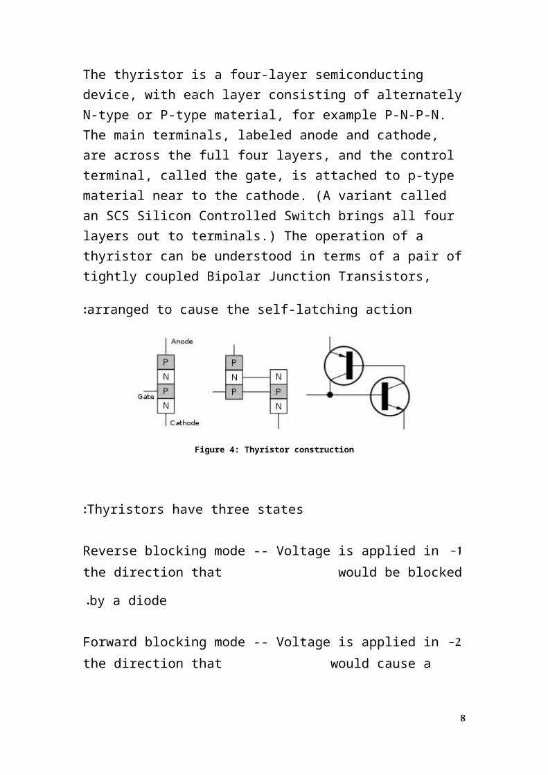
The thyristor is a four-layer semiconducting device, with each layer consisting of alternately N-type or P-type material, for example P-N-P-N. The main terminals, labeled anode and cathode, are across the full four layers, and the control terminal, called the gate, is attached to p-type material near to the cathode. (A variant called an SCS Silicon Controlled Switch brings all four layers out to terminals.) The operation of a thyristor can be understood in terms of a pair of tightly coupled Bipolar Junction Transistors, arranged to cause the self-latching action:
Figure 4: Thyristor construction
Thyristors have three states:
1 -Reverse blocking mode -- Voltage is applied in the direction that would be blocked by a diode .
2 -Forward blocking mode -- Voltage is applied in the direction that would cause a diode to conduct, but the thyristor has not yet been triggered into conduction .
3 -Forward conducting mode -- The thyristor has been triggered into conduction and will remain conducting until the forward current drops
below a threshold value known as the "holding current "
6

Function of the gate terminal:
The thyristor has three p-n junctions (serially named J1, J2, J3 from the anode).
Figure 5: Layer diagram of thyristor
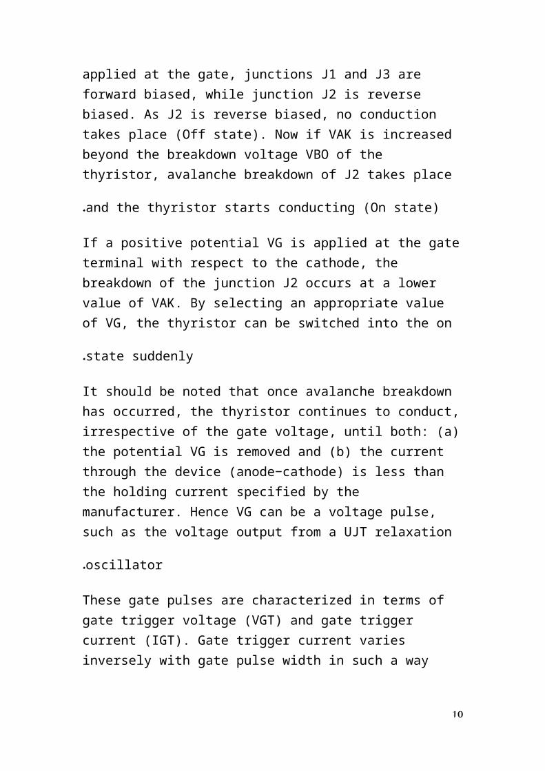
When the anode is at a positive potential VAK with respect to the cathode with no voltage applied at the gate, junctions J1 and J3 are forward biased, while junction J2 is reverse biased. As J2 is reverse biased, no conduction takes place (Off state). Now if VAK is increased beyond the breakdown voltage VBO of the thyristor, avalanche breakdown of J2 takes place and the thyristor starts conducting (On state).
If a positive potential VG is applied at the gate terminal with respect to the cathode, the breakdown of the junction J2 occurs at a lower value of VAK. By selecting an appropriate value of VG, the thyristor can be switched into the on state suddenly.
It should be noted that once avalanche breakdown has occurred, the thyristor continues to conduct, irrespective of the gate voltage, until both: (a) the potential VG is removed and (b) the current through the device (anode−cathode) is less than the holding current specified by the manufacturer. Hence VG can be a voltage pulse, such as the voltage output from a UJT relaxation oscillator.
7

These gate pulses are characterized in terms of gate trigger voltage (VGT) and gate trigger current (IGT). Gate trigger current varies inversely with gate pulse width in such a way that it is evident that there is a minimum gate charge required to trigger the thyristor.
Switching characteristics:
A thyristor is turn on by increasing the anode current .this can be accomplished in one of the following ways:
1-light.
2- high voltage.
dv/dt.-3
4-gate current.
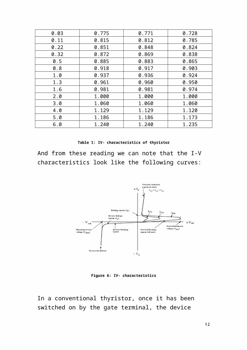
We use the gate current method to turn on the thyristor which we decided to work on (TIC116) which has the datasheet at the end of this report and to study it's I-V characteristics by the following circuit:
From this circuit we have the following readings:
VAK(VG=10v)VAK(VG=6.5v)VAK(VG=3.5v)IT0.6320.7150.7360.010.7280.7710.7750.030.7850.8120.8150.110.8240.8480.8510.220.8380.8690.8720.320.8650.8830.8850.50.9030.9170.9180.80.9240.9360.9371.00.9500.9600.9611.3
8

0.9740.9810.9811.61.0001.0001.0002.01.0601.0601.0603.01.1201.1291.1294.01.1731.1861.1865.01.2351.2401.2406.0
Table 1: IV- characteristics of thyristor
And from these reading we can note that the I-V characteristics look like the following curves:
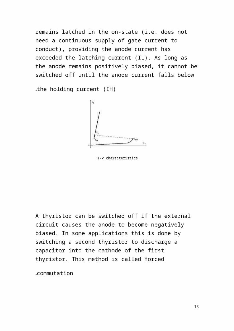
Figure 6: IV- characteristics
In a conventional thyristor, once it has been switched on by the gate terminal, the device remains latched in the on-state (i.e. does not need a continuous supply of gate current to conduct), providing the anode current has exceeded the latching current (IL). As long as the anode remains positively biased, it cannot be switched off until the anode current falls below the holding current (IH).
9
I-V characteristics:
A thyristor can be switched off if the external circuit causes the anode to become negatively biased. In some applications this is done by switching a second thyristor to discharge a capacitor into the cathode of the first thyristor. This method is called forced commutation.
After a thyristor has been switched off by forced commutation, a finite time delay must have elapsed before the anode can be positively biased in the off-state. This minimum delay is called the circuit commutated turn off time (tQ). Attempting to positively bias the anode within this time causes the thyristor to be self-triggered by the remaining charge carriers (holes and electrons) that have not yet recombined.
For applications with frequencies higher than the domestic AC mains supply (e.g. 50 Hz or 60 Hz), thyristors with lower values of tQ are required. Such fast thyristors are made by diffusing into the silicon heavy metals ions such as gold or platinum which act as charge combination centres. Alternatively, fast thyristors may be made by neutron irradiation of the silicon.
10

2.2 :Thyristor Triggering Circuit
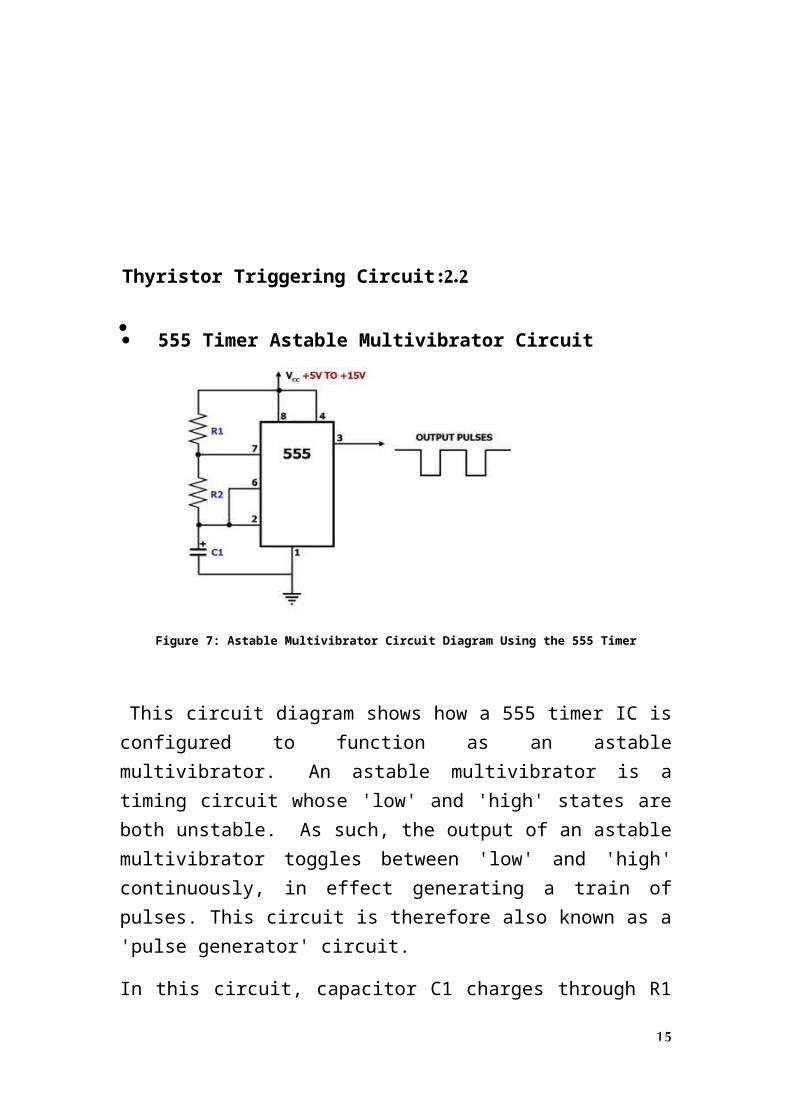
555 Timer Astable Multivibrator Circuit
Figure 7: Astable Multivibrator Circuit Diagram Using the 555 Timer
This circuit diagram shows how a 555 timer IC is configured to function as an astable multivibrator. An astable multivibrator is a timing circuit whose 'low' and 'high' states are both unstable. As such, the output of an astable multivibrator toggles between 'low' and 'high' continuously, in effect generating a train of pulses. This circuit is therefore also known as a 'pulse generator' circuit.
In this circuit, capacitor C1 charges through R1 and R2, eventually building up enough voltage to trigger an internal comparator to toggle the
11
output flip-flop. Once toggled, the flip-flop discharges C1 through R2 into pin 7, which is the discharge pin. When C1's voltage becomes low enough, another internal comparator is triggered to toggle the output flip-flop. This once again allows C1 to charge up through R1 and R2 and the cycle starts all over again.
C1's charge-up time t1 is given by: t1 = 0.693(R1+R2)C1.
C1's discharge time t2 is given by: t2 = 0.693(R2)C1.
Thus, the total period of one cycle is t1+t2 = 0.693 C1(R1+2R2).
The frequency f of the output wave is the reciprocal of this period, and is therefore given by:
f = 1.44/(C1(R1+2R2)), wherein f is in Hz if R1 and R2 are in megaohms and C1 is in microfarads.
555 Timer Monostable Multivibrator Circuit
Figure 8: Monostable Multivibrator Circuit Diagram Using the 555 Timer
This circuit diagram shows how a 555 timer IC is configured to function as a basic monostable multivibrator. A monostable multivibrator is a timing circuit that changes state once triggered, but returns to its original state after a certain time delay. It got its name from the fact that only one of its output states is stable. It is
12

also known as a 'one-shot'. In this circuit, a negative pulse applied at pin 2 triggers an internal flip-flop that turns off pin 7's discharge transistor, allowing C1 to charge up through R1. At the same time, the flip-flop brings the output (pin 3) level to 'high'. When capacitor C1 as charged up to about 2/3 Vcc, the flip-flop is triggered once again, this time making the pin 3 output 'low' and turning on pin 7's discharge transistor, which discharges C1 to ground. This circuit, in effect, produces a pulse at pin 3 whose width t is just the product of R1 and C1, i.e., t=R1C1. The reset pin, which may be used to reset the timing cycle by pulling it momentarily low, should be tied to the Vcc if it will not be used.
Unijunction Transistor Relaxation Oscillator
Figure 9: Unijunction transistor relaxation oscillator and waveforms. Oscillator drives SCR
During capacitor discharge through the E-B1 saturation resistance, a pulse may be seen on the external B1 and B2 load resistors, Figure above. The load resistor at B1 needs to be low to not affect the discharge time. The external resistor at B2 is optional. It may be replaced by a short circuit. The approximate frequency is given by 1/f = T = RC. A more accurate expression for frequency is given in Figure above .
The charging resistor RE must fall within certain limits. It must be small enough to allow IP to flow based on the VBB supply less VP. It must be
13
large enough to supply IV based on the VBB supply less VV. [MHW] The equations and an example for a 2n2647:
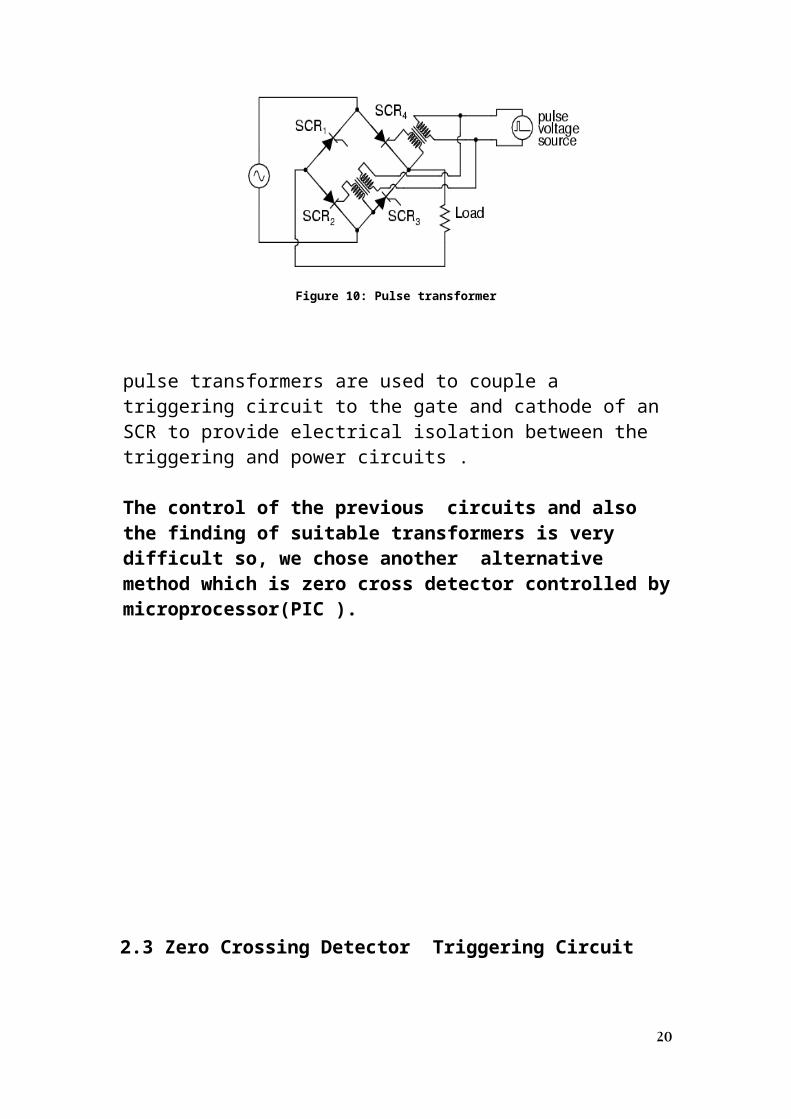
Pulse transformer:
All the previous circuits are used as a pulse generators and cannot be used to trigger the thyristors immediately so, we need to use pulse transformers in order to achieve a correct trigger for the thyristors as shown in the following figure .
Figure 10: Pulse transformer
pulse transformers are used to couple a triggering circuit to the gate and cathode of an SCR to provide electrical isolation between the triggering and power circuits .
14
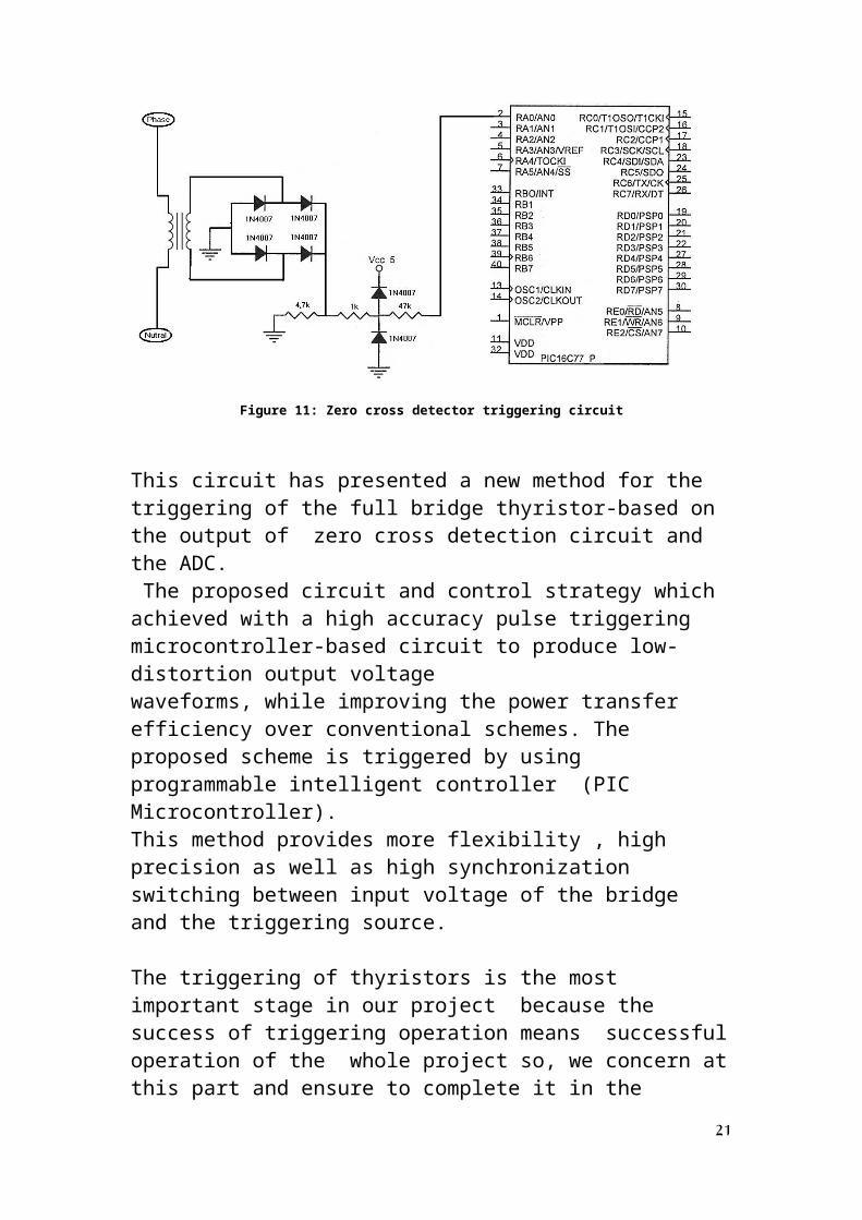
The control of the previous circuits and also the finding of suitable transformers is very difficult so, we chose another alternative method which is zero cross detector controlled by microprocessor(PIC ).
2.3 Zero Crossing Detector Triggering Circuit
Figure 11: Zero cross detector triggering circuit
This circuit has presented a new method for the triggering of the full bridge thyristor-based on the output of zero cross detection circuit and the ADC. The proposed circuit and control strategy which achieved with a high accuracy pulse triggering microcontroller-based circuit to produce low-distortion output voltage
15

waveforms, while improving the power transfer efficiency over conventional schemes. The proposed scheme is triggered by using programmable intelligent controller (PIC Microcontroller). This method provides more flexibility , high precision as well as high synchronization switching between input voltage of the bridge and the triggering source.
The triggering of thyristors is the most important stage in our project because the success of triggering operation means successful operation of the whole project so, we concern at this part and ensure to complete it in the correct way by dividing the work into several steps:
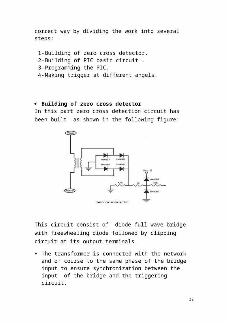
1- Building of zero cross detector.2- Building of PIC basic circuit .3- Programming the PIC.4- Making trigger at different angels.
Building of zero cross detectorIn this part zero cross detection circuit has been built as shown in the following figure:
This circuit consist of diode full wave bridge with freewheeling diode followed by clipping circuit at its output terminals.
16
The transformer is connected with the network and of course to the same phase of the bridge input to ensure synchronization between the input of the bridge and the triggering circuit.
The diode bridge is use to rectify the transformer output voltage and to convert the input of the PIC from ac voltage to dc voltage because the PIC cannot deal with the ac voltage .
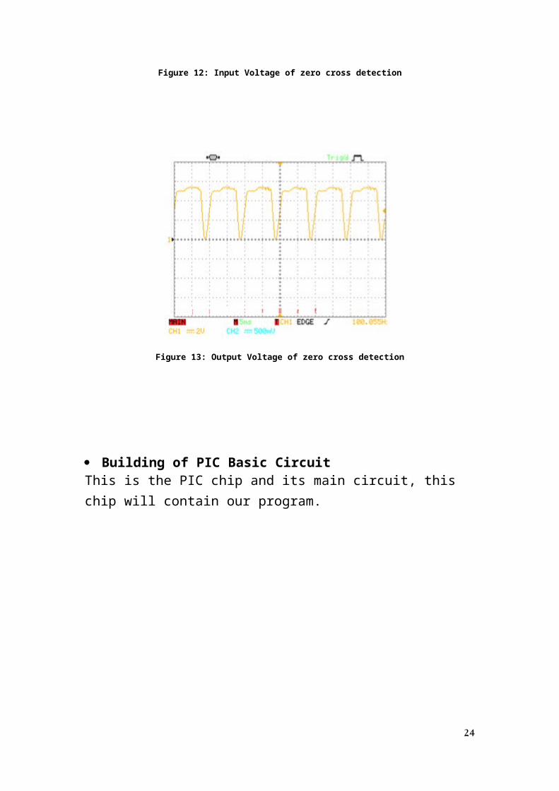
The freewheeling diode is used to ensure removing of the negative voltage.
The clipping circuit her prevent the PIC input from increasing above Vcc.
The input and output of this circuit are shown in the following figures :
Figure 12: Input Voltage of zero cross detection
17
Figure 13: Output Voltage of zero cross detection
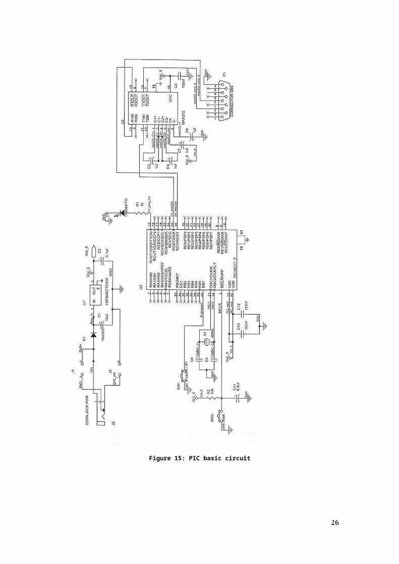
Building of PIC Basic CircuitThis is the PIC chip and its main circuit, this chip will contain our program.
18
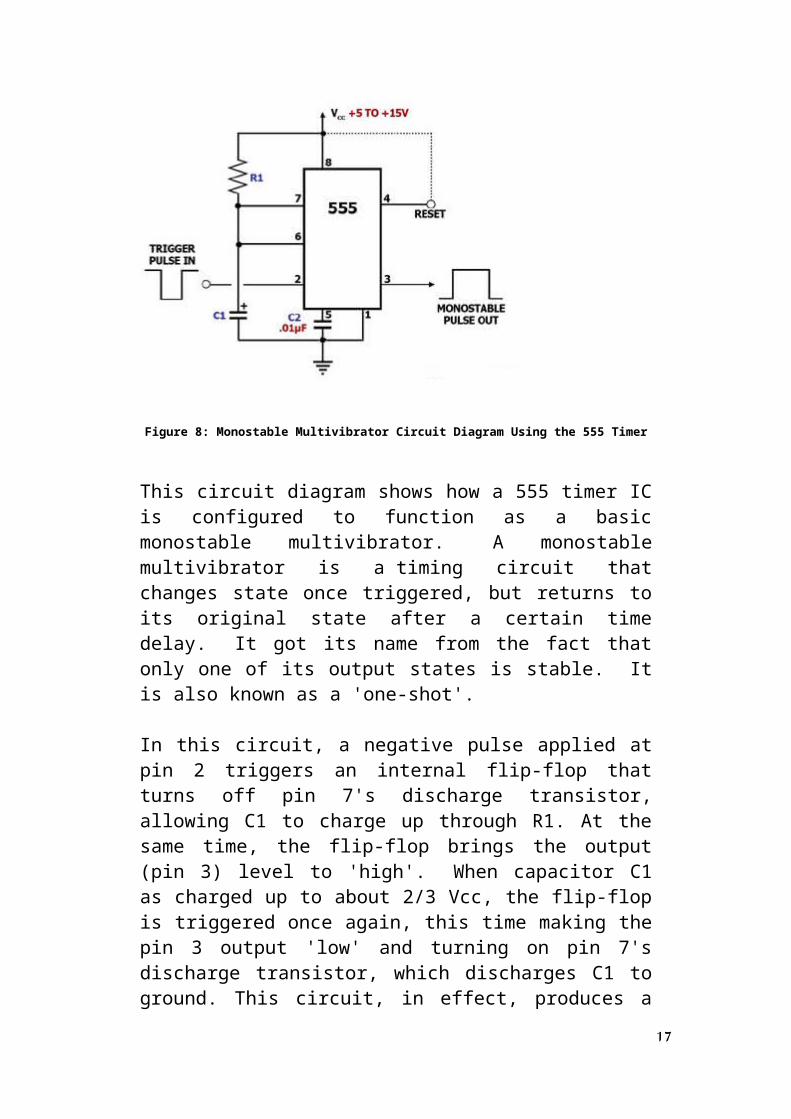
Figure 14: PIC chip
After building the zero cross detection circuit the PIC basic circuit will be built as shown in the following figure:
19
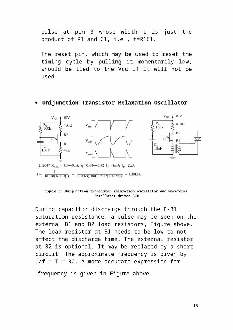
Figure 15: PIC basic circuit
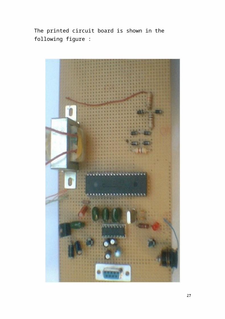
The printed circuit board is shown in the following figure :
20
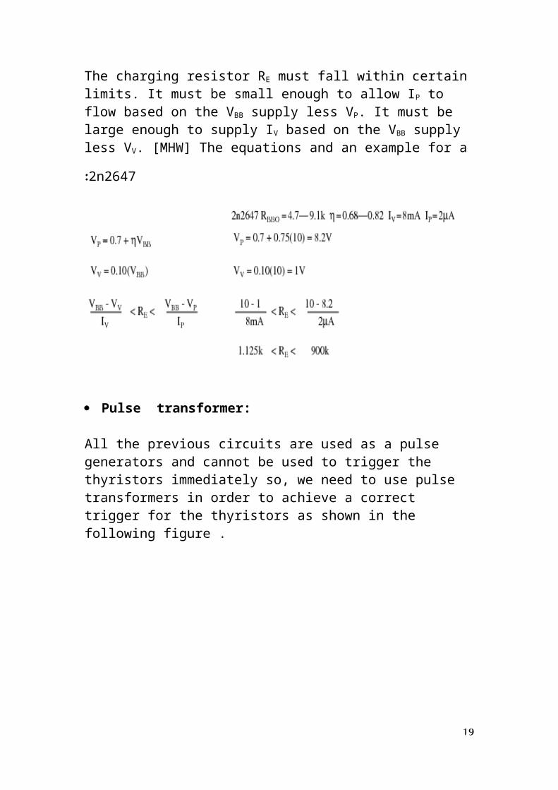
Figure 16: printed circuit board of the PIC basic circuit
Programming the PICThe principle of this circuit is to read the voltage value from the output of the rectifier after clipping and convert it to digital by the
21
ADC in the PIC then compare it with zero to make the time when of zero crossing as reference for the triggering.
The flow chart for programming:
Figure 17: Flow chart for triggering thyristor
Now the basic program for triggering one thyristor is written as the following:
#include "C:\Documents and Settings\Administrator\Desktop\single\1phase.h"
22
void main()
int16 value1,value2;
setup_adc_ports(AN0);
setup_adc(ADC_CLOCK_DIV_2);
setup_psp(PSP_DISABLED);
setup_spi(FALSE);
setup_timer_0(RTCC_INTERNAL);
setup_wdt(WDT_18MS);
setup_timer_1(T1_DISABLED);
setup_timer_2(T2_DISABLED,0,1);
setup_comparator(NC_NC_NC_NC);
setup_vref(VREF_LOW|-2);
while(true)
value1=read_adc();
if((value1>=10) & (value1<=40)) //this is adc vaule to find the zero
value2=read_adc();
if (value2>=value1)
delay_us(0000); //this delay control the delay time
output_high(pin_d1);
delay_us(500);
output_low(pin_d1);
restart_wdt();
restart_wdt();
restart_wdt();
restart_wdt();
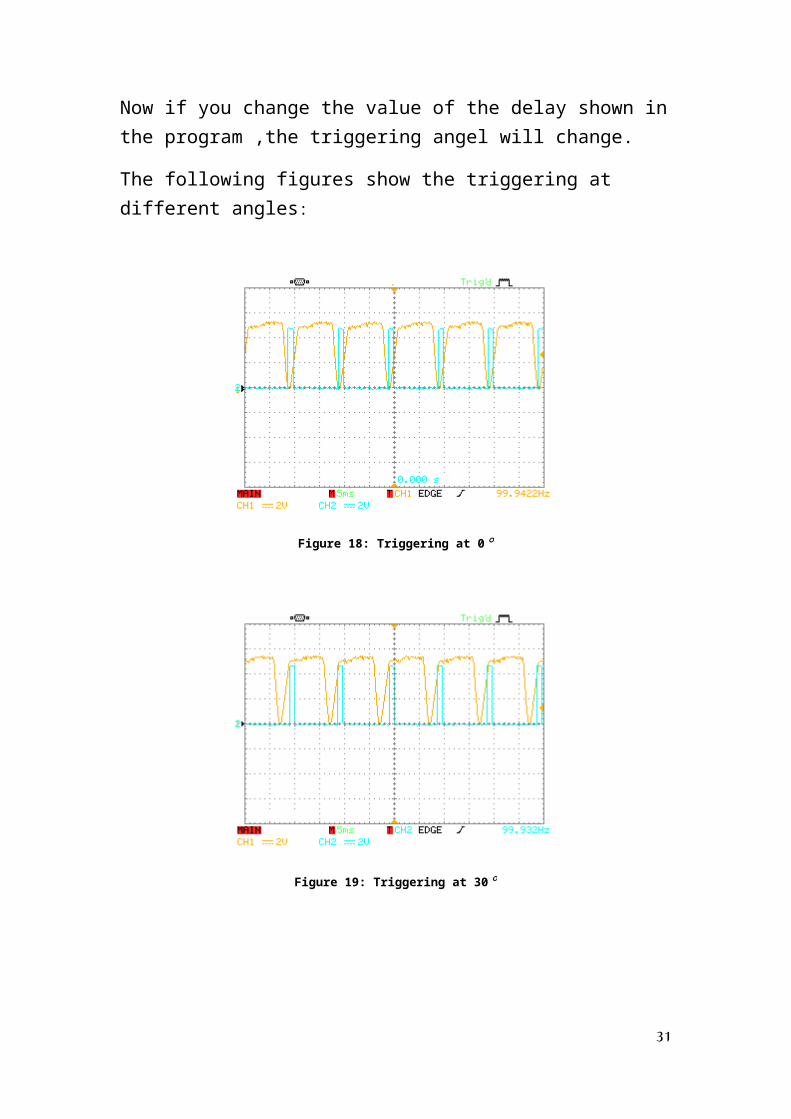
Making trigger at different angels.Now if you change the value of the delay shown in the program ,the triggering angel will change.
23
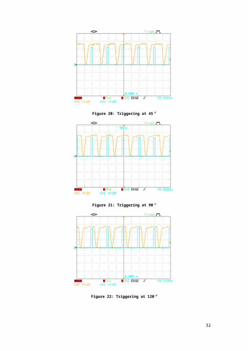
The following figures show the triggering at different angles:
Figure 18: Triggering at 0°
Figure 19: Triggering at 30°
24
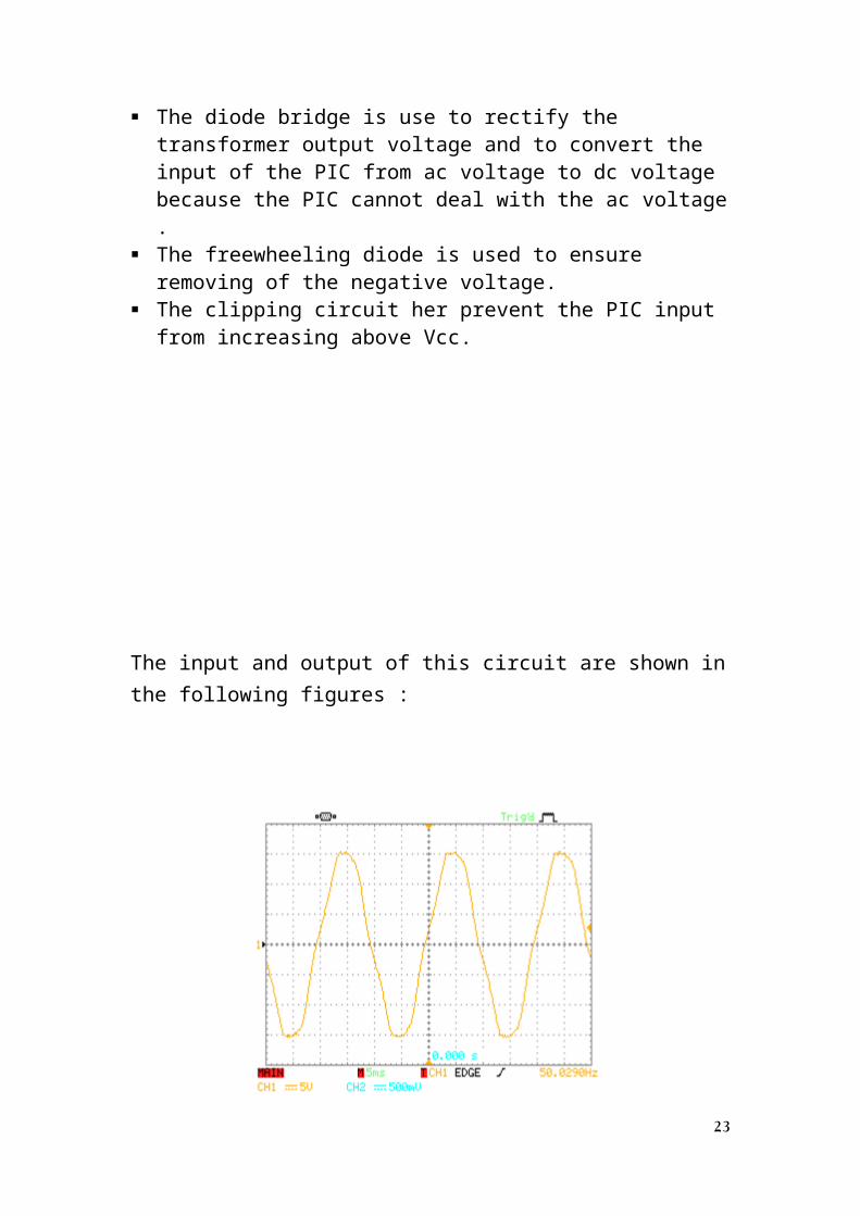
Figure 20: Triggering at 45°
Figure 21: Triggering at 90°
Figure 22: Triggering at 120°
25
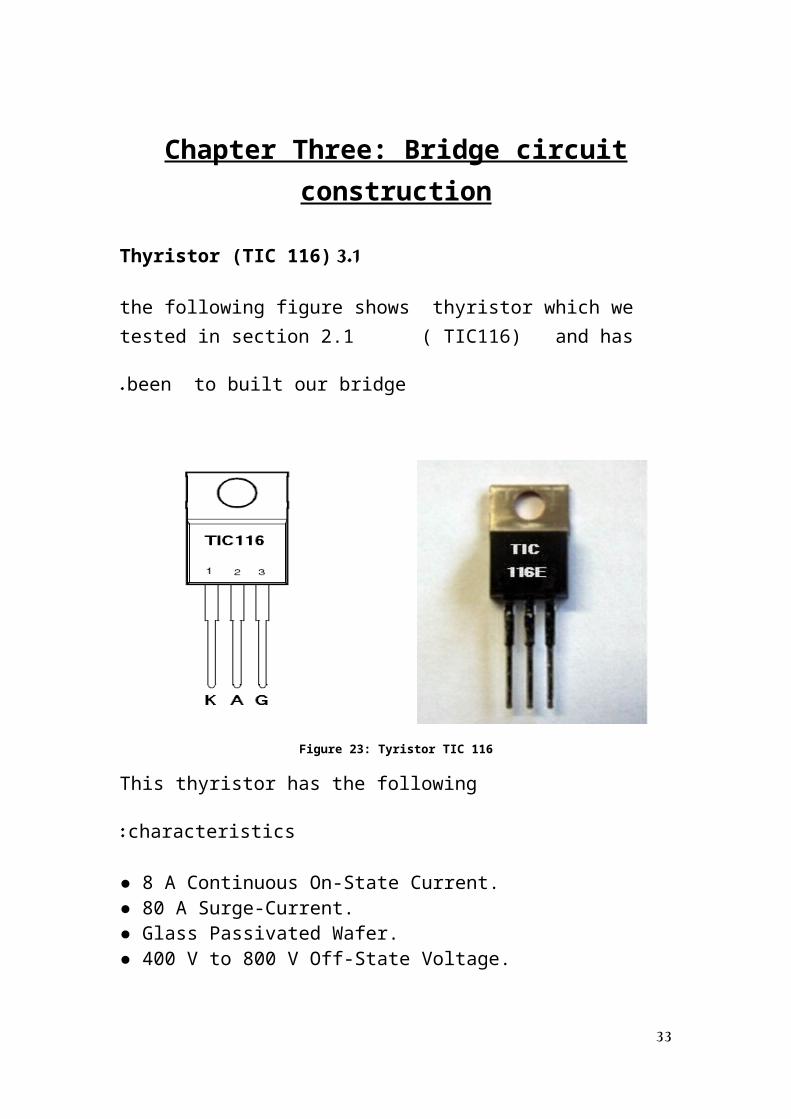
Chapter Three: Bridge circuit construction3.1 Thyristor (TIC 116)
the following figure shows thyristor which we tested in section 2.1 ( TIC116) and has been to built our bridge.
Figure 23: Tyristor TIC 116
This thyristor has the following characteristics:
8 A Continuous On-State Current. 80 A Surge-Current. Glass Passivated Wafer. 400 V to 800 V Off-State Voltage.
Max IGT of 20 mA.
Again for more details you can return to the datasheet at the appendix.
Notes:
1 -8 amps continuous on-state current is depending on the load to be
supplied at the output of the bridge ( Idrms=Vdrms
R ).
2- 400 V to 800V off-state voltage to limit the peak inverse voltage of the thyristor (PIV=2√3Vm).
3 - Max IGT this value is to chose the gate current depending on the I-V curves .
26

3.2 The circuit operation:
3.2.1 Single-phase fully- controlled bridge rectifier circuit with a resistive load:
This section describes the operation of a single-phase fully- controlled bridge rectifier circuit with a resistive load. The operation of this circuit can be understood more easily when the load is purely resistive. The analysis in this page is based on the assumption that the SCRs are ideal controlled switches. It means that when the SCRs are ON, the ON-state voltage drops are zero. In the OFF- state, the leakage current is assumed to be zero. The main purpose of the fully-controlled bridge rectifier circuit is to provide a variable dc voltage from an ac source.
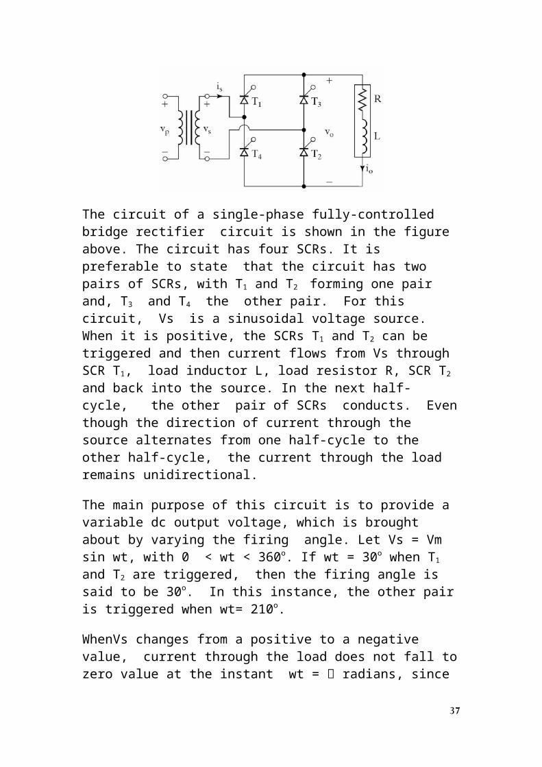
The circuit of a single-phase fully-controlled bridge rectifier circuit is shown in the figure above. The circuit has four SCRs. It is preferable to state that the circuit has two pairs of SCRs, with T1 and T2 forming one pair and, T3 and T4 the other pair. For this circuit, the source is marked as vs and it is a sinusoidal voltage source. When it is positive, SCRs T1 and T2 can be triggered and then current flows from vs through SCR T1, load resistor R, SCR T2 and back into the source. In the next half-cycle, the other pair of SCRs conducts. Even though the direction of current through the source alternates from one half-cycle to the other half-cycle, the current through the load remains unidirectional.
The main purpose of this circuit is to provide a variable dc output voltage, which is brought about by varying the firing angle. LetVs = Vm Sin wt, with 0 < wt < 360o. If wt = 30o when T1 and T2 are triggered, then the firing angle is said to be 30o. In this instance, the other pair is triggered when wt = 210o.
27
When Vs changes from a positive to a negative value, the current through the load becomes zero at the instant wt = radians, since the load is purely resistive and the SCRs cease to conduct. After that there is no current flow till the other pair is triggered. Hence the conduction or current flow through the load is discontinuous.
3.2.2 single-phase fully- controlled bridge rectifier circuit with a load consisting of both a resistor and an inductor in series:
This section describes the operation of a single-phase fully- controlled bridge rectifier circuit with a load consisting of both a resistor and an inductor in series. The analysis in this page is based on the assumption that the SCRs are ideal controlled switches. The main purpose of the fully-controlled bridge rectifier circuit is to provide a variable dc voltage from an ac source.
The circuit of a single-phase fully-controlled bridge rectifier circuit is shown in the figure above. The circuit has four SCRs. It is preferable to state that the circuit has two pairs of SCRs, with T1 and T2 forming one pair and, T3 and T4 the other pair. For this circuit, Vs is a sinusoidal voltage source. When it is positive, the SCRs T1 and T2 can be triggered and then current flows from Vs through SCR T1, load inductor L, load resistor R, SCR T2 and back into the source. In the next half-cycle, the other pair of SCRs conducts. Even though the direction of current through the source alternates from one half-cycle to the other half-cycle, the current through the load remains unidirectional.
The main purpose of this circuit is to provide a variable dc output voltage, which is brought about by varying the firing angle. Let Vs = Vm sin wt, with 0 < wt < 360o. If wt = 30o when T1 and T2 are triggered, then the firing angle is said to be 30o. In this instance, the other pair is triggered when wt= 210o.
28
WhenVs changes from a positive to a negative value, current through the load does not fall to zero value at the instant wt = radians, since the load contains an inductor and the SCRs continue to conduct, with the inductor acting as a source. When the current through an inductor is falling, the voltage across it changes sign compared with the sign that exists when its current is rising. When the current through the inductor is falling, its voltage is such that the inductor delivers power to the load resistor, feeds back some power to the ac source under certain conditions and keeps the SCRs in conduction forward-biased. If the firing angle is less than the load angle, the energy stored in the inductor is sufficient to maintain conduction till the next pair of SCRs is triggered. When the firing angle is greater than the load angle, the current through the load becomes zero and the conduction through the load becomes discontinuous. Usually the description of this circuit is based on the assumption that the load inductance is sufficiently large to keep the load current continuous and ripple-free.
3.3 Triggering transportation:
Now our project is divided into two parts the first part consists of the control part (the zero cross and the PIC) and the second part consists of the thyristors bridge ,then we need to connect the two parts by using a suitable interface.
We built several circuits in order to make this connection , one of them worked properly, but the others failed, at this section we will explain those methods.
The failure methods:
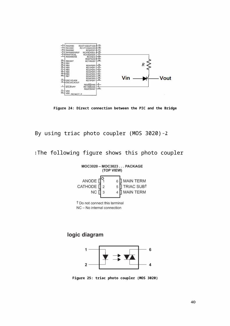
1 -Directly connection between the PIC and the Bridge:In this method we connect the gate of the thyristor to a high output pin of the PIC through resistor and the anode to a low output pin of the PIC , there are two problems here the first one is that the resistance between the PIC pins is very small at high input voltage, the second is that the gate of the thyristor is connected to its cathode by a small resistance this mean that the input voltage of the bridge is connected to the PIC pins, as a result the PIC damaged because the PIC can not stand with any voltage higher than 5 volt.
29

The following figure shows the connection of this method:
Figure 24: Direct connection between the PIC and the Bridge
2 -By using triac photo coupler (MOS 3020)
The following figure shows this photo coupler:
Figure 25: triac photo coupler (MOS 3020)
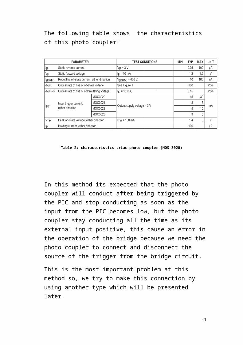
The following table shows the characteristics of this photo coupler:
30
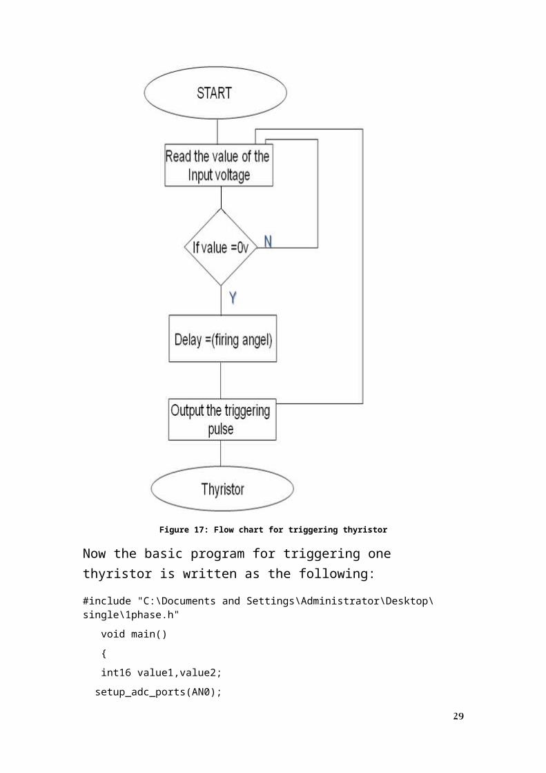
Table 2: characteristics triac photo coupler (MOS 3020)
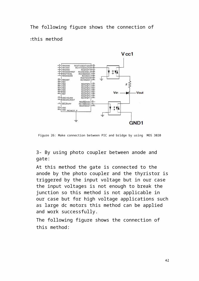
In this method its expected that the photo coupler will conduct after being triggered by the PIC and stop conducting as soon as the input from the PIC becomes low, but the photo coupler stay conducting all the time as its external input positive, this cause an error in the operation of the bridge because we need the photo coupler to connect and disconnect the source of the trigger from the bridge circuit.
This is the most important problem at this method so, we try to make this connection by using another type which will be presented later.
The following figure shows the connection of this method:
31

Figure 26: Make connection between PIC and bridge by using MOS 3020
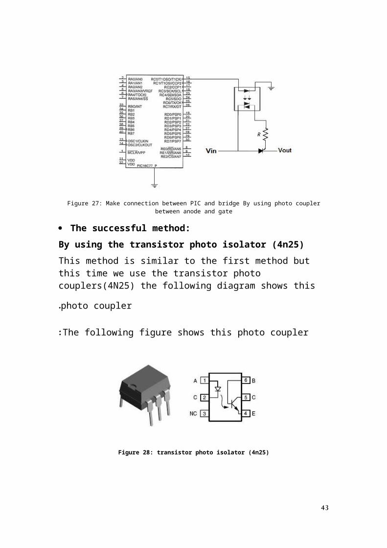
3- By using photo coupler between anode and gate:At this method the gate is connected to the anode by the photo coupler and the thyristor is triggered by the input voltage but in our case the input voltages is not enough to break the junction so this method is not applicable in our case but for high voltage applications such as large dc motors this method can be applied and work successfully.The following figure shows the connection of this method:
Figure 27: Make connection between PIC and bridge By using photo coupler between anode and gate
32
The successful method: By using the transistor photo isolator (4n25)This method is similar to the first method but this time we use the transistor photo couplers(4N25) the following diagram shows this photo coupler.The following figure shows this photo coupler:
Figure 28: transistor photo isolator (4n25)
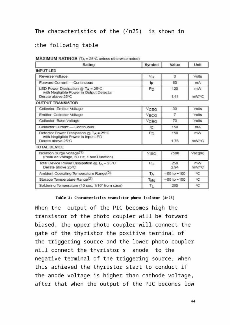
The characteristics of the (4n25) is shown in the following table:
Table 3: Characteristics transistor photo isolator (4n25)
33
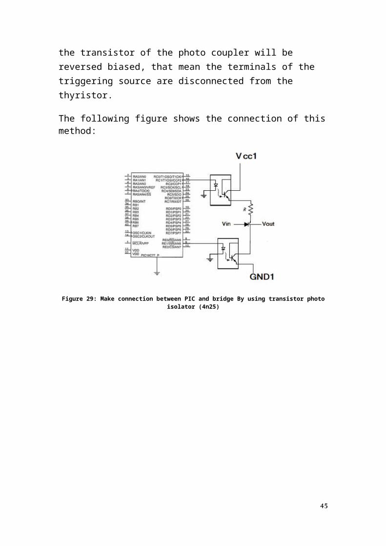
When the output of the PIC becomes high the transistor of the photo coupler will be forward biased, the upper photo coupler will connect the gate of the thyristor the positive terminal of the triggering source and the lower photo coupler will connect the thyristor's anode to the negative terminal of the triggering source, when this achieved the thyristor start to conduct if the anode voltage is higher than cathode voltage, after that when the output of the PIC becomes low the transistor of the photo coupler will be reversed biased, that mean the terminals of the triggering source are disconnected from the thyristor.
The following figure shows the connection of this method:
Figure 29: Make connection between PIC and bridge By using transistor photo isolator (4n25)
34
3.4 The complete circuit of the project:The following figure shows the complete circuit of our project:
Figure 30: The complete circuit of the project
35
The printed circuit board of our complete circuit is shown in the following figures :
36
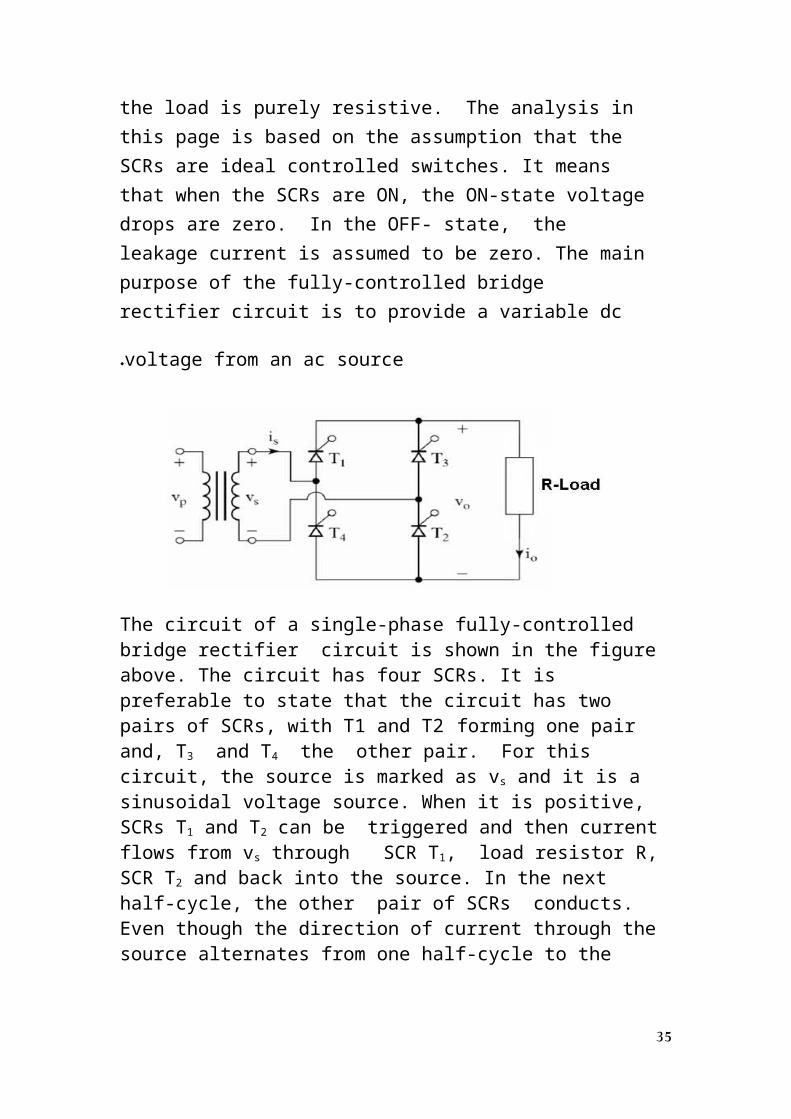
Figure 31: printed circuit board of complete circuit
37
The complete code for triggering all thyristors:
#include "C:\Documents and Settings\Administrator\Desktop\single phase\1phase2.h"
void main()
int16 value1,value2;
int16 value3=5;
setup_adc_ports(AN0);
setup_adc(ADC_CLOCK_DIV_2);
setup_psp(PSP_DISABLED);
setup_spi(FALSE);
setup_timer_0(RTCC_INTERNAL);setup_wdt(WDT_18MS);
setup_timer_1(T1_DISABLED);
setup_timer_2(T2_DISABLED,0,1);
setup_comparator(NC_NC_NC_NC);
setup_vref(FALSE);
while(true)
if( input(PIN_B0) )
value3=0;
if( input(PIN_B1) )
value3=45;
if( input(PIN_B2) )
value3=90;
if( input(PIN_B3) )
value3=135;
38
while(value3==0)
value1=read_adc();
if((value1>=20) & (value1<=60))
value2=read_adc();
if (value2>value1)
delay_us(0000);
output_high(pin_d1);
output_high(pin_d2);
output_high(pin_d4);
output_high(pin_d5);
delay_us(1500);
output_low(pin_d1);
output_low(pin_d2);
output_low(pin_d4);
output_low(pin_d5);
delay_us(8500);
output_high(pin_d4);
output_high(pin_d0);
output_high(pin_d7);
output_high(pin_d6);
39
delay_us(500);
output_low(pin_d4);
output_low(pin_d0);
output_low(pin_d7);
output_low(pin_d6);
if( input(PIN_B0) )
value3=0;
if( input(PIN_B1) )
value3=45;
if( input(PIN_B2) )
value3=90;
if( input(PIN_B3) )
value3=135;
restart_wdt();
restart_wdt();
restart_wdt();
while(value3==45)
value1=read_adc();
if((value1>=20) & (value1<=60))
value2=read_adc();
if (value2>value1)
40

delay_us(2500);
output_high(pin_d1);
output_high(pin_d2);
output_high(pin_d4);
output_high(pin_d5);
delay_us(500);
output_low(pin_d1);
output_low(pin_d2);
output_low(pin_d4);
output_low(pin_d5);
delay_us(9500);
output_high(pin_d4);
output_high(pin_d0);
output_high(pin_d7);
output_high(pin_d6);
delay_us(500);
output_low(pin_d4);
output_low(pin_d0);
output_low(pin_d7);
output_low(pin_d6);
if( input(PIN_B0) )
value3=0;
41
if( input(PIN_B1) )
value3=45;
if( input(PIN_B2) )
value3=90;
if( input(PIN_B3) )
value3=135;
restart_wdt();
restart_wdt();
restart_wdt();
while(value3==90)
value1=read_adc();
if((value1>=20) & (value1<=60))
value2=read_adc();
if (value2>value1)
delay_us(5000);
output_high(pin_d1);
output_high(pin_d2);
output_high(pin_d4);
output_high(pin_d5);
42
delay_us(500);
output_low(pin_d1);
output_low(pin_d2);
output_low(pin_d4);
output_low(pin_d5);
delay_us(9500);
output_high(pin_d4);
output_high(pin_d0);
output_high(pin_d7);
output_high(pin_d6);
delay_us(500);
output_low(pin_d4);
output_low(pin_d0);
output_low(pin_d7);
output_low(pin_d6);
if( input(PIN_B0) )
value3=0;
if( input(PIN_B1) )
value3=45;
if( input(PIN_B2) )
value3=90;
if( input(PIN_B3) )
value3=135;
43
restart_wdt();
restart_wdt();
restart_wdt();
while(value3==135)
value1=read_adc();
if((value1>=20) & (value1<=60))
value2=read_adc();
if (value2>value1)
delay_us(7500);
output_high(pin_d1);
output_high(pin_d2);
output_high(pin_d4);
output_high(pin_d5);
delay_us(500);
output_low(pin_d1);
output_low(pin_d2);
output_low(pin_d4);
output_low(pin_d5);
44
delay_us(9500);
output_high(pin_d4);
output_high(pin_d0);
output_high(pin_d7);
output_high(pin_d6);
delay_us(500);
output_low(pin_d4);
output_low(pin_d0);
output_low(pin_d7);
output_low(pin_d6);
if( input(PIN_B0) )
value3=0;
if( input(PIN_B1) )
value3=45;
if( input(PIN_B2) )
value3=90;
if( input(PIN_B3) )
value3=135;
restart_wdt();
restart_wdt();
restart_wdt();
45
restart_wdt();
restart_wdt();
46
Chapter Four: Investigation about the input and output characteristics:
After finishing the project hardware, the circuit input and output will to be tested under several loads and different firing angels.This stage is divided into different parts:
1- Pure resistive load.2- R-L load.3- DC motor speed control.4- Filtering the grid current.
4.1 :investigation input and output characteristics of pure resistive load:
In this section we apply resistive load on the output of the bridge and we get the waveforms from the oscilloscope, the output voltage and input
current at different firing angle will be shown in the following figures:
following figures show the output voltage at different firing angle, input voltage (Vin)= 20 v and R= 16Ω:
47
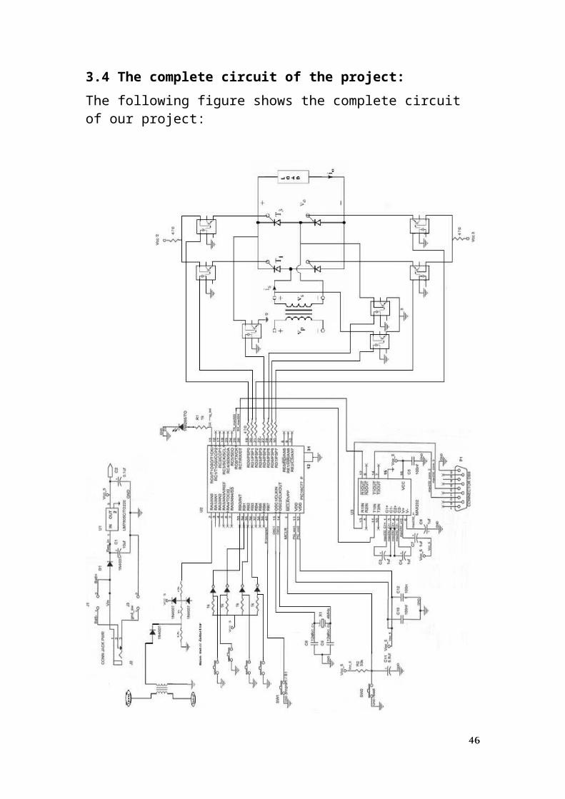
Figure 32: Output voltage form at R=16, α = zero°
Figure 33: Output voltage form at R=16, α = 45°
Figure 34: Output voltage form at R=16, α = 90°
48
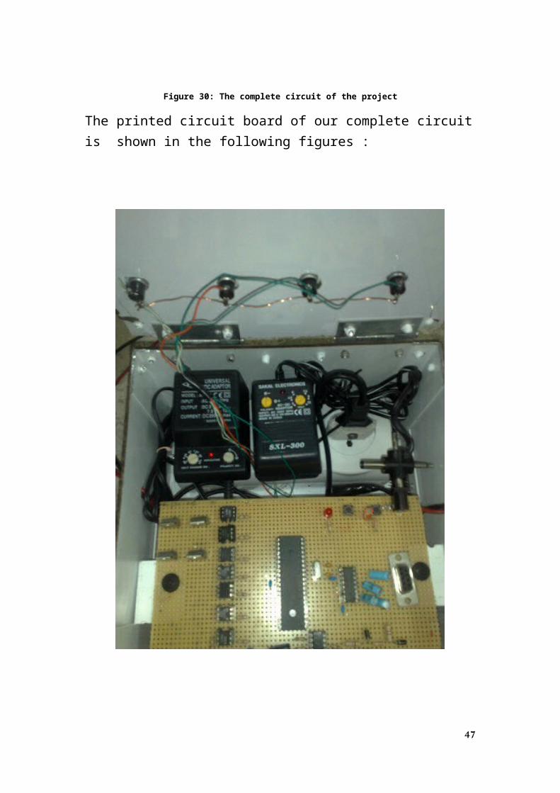
Figure 35: Output voltage form at R=16, α = 135°
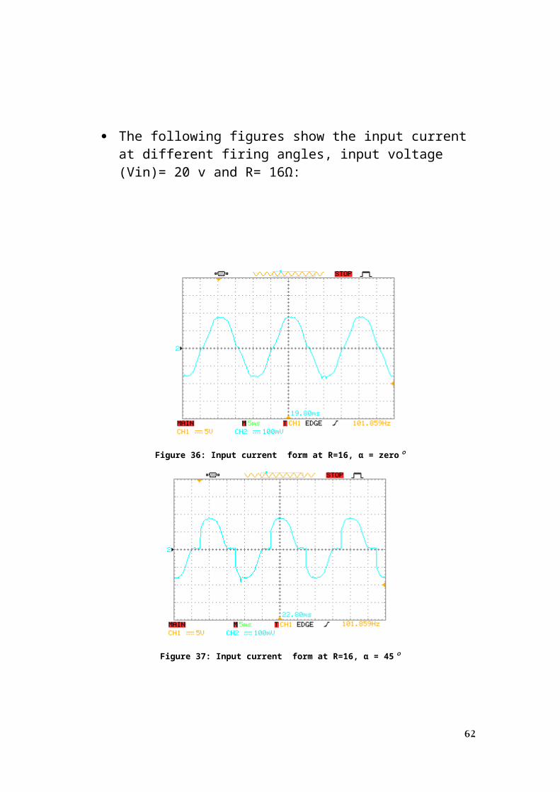
The following figures show the input current at different firing angles, input voltage (Vin)= 20 v and R= 16Ω:
Figure 36: Input current form at R=16, α = zero°
49
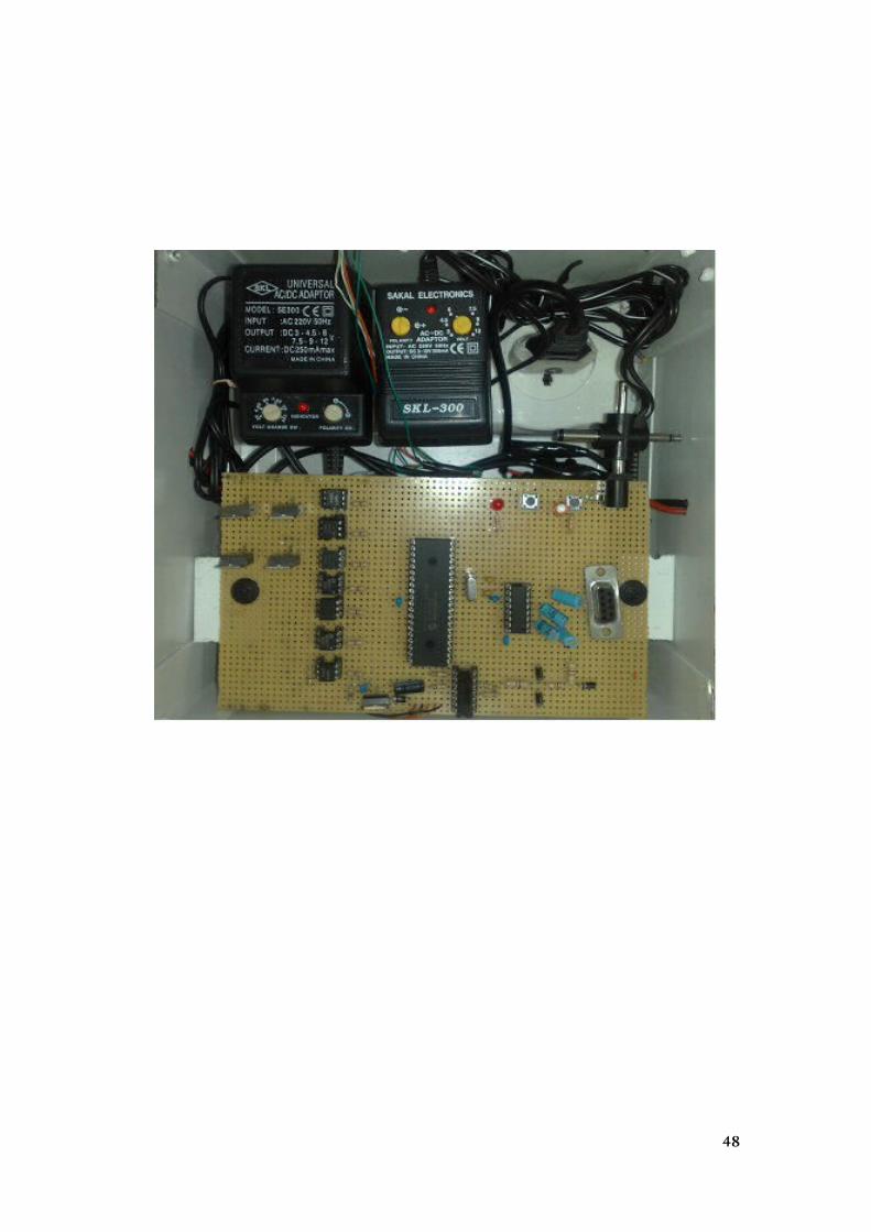
Figure 37: Input current form at R=16, α = 45°
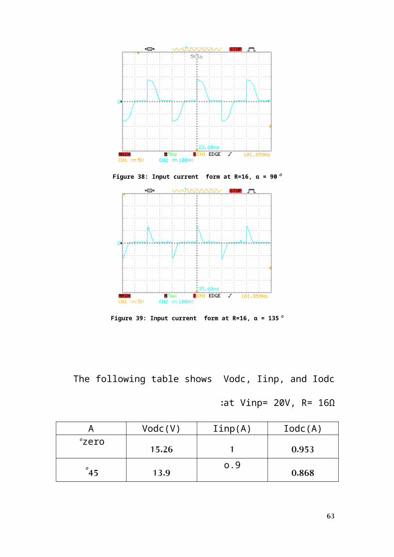
Figure 38: Input current form at R=16, α = 90°
Figure 39: Input current form at R=16, α = 135°
50

The following table shows Vodc, Iinp, and Iodc at Vinp= 20V, R= 16Ω:
Α Vodc(V) Iinp(A) Iodc(A)zero° 15.26 1 0.95345° 13.9 o.9 0.86890° 8.33 0.76 0.520135° 2.5 0.35 0.156
Table 4: Vodc, Iinp, and Iodc at Vinp= 20V, R= 16Ω and different firing angles
4.2: investigation input and output characteristics of R-L load:
In this section we apply R-L load on the output of the bridge and we get the waveforms from the oscilloscope, the output voltage and input current
at different firing angle will be shown in the following figures: The following figures show the output voltage at different firing
angle, input voltage (Vin)= 20v, L=70mh and R= 16Ω, Ф= 53.9°:
Figure 40: Output voltage form at Ф= 53.9°, α = zero°
51

Figure 41: Output voltage form at Ф= 53.9°, α = 45°
Figure 42: Output voltage form at Ф= 53.9°, α = 90°
Figure 43: Output voltage form at Ф= 53.9°, α = 135°
52

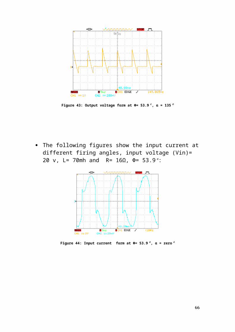
The following figures show the input current at different firing angles, input voltage (Vin)= 20 v, L= 70mh and R= 16Ω, Ф= 53.9°:
Figure 44: Input current form at Ф= 53.9°, α = zero°
Figure 45: Input current form at Ф= 53.9°, α = 45°
Figure 46: Input current form at Ф= 53.9°, α = 90°
53

Figure 47: Input current form at Ф= 53.9°, α = 135°
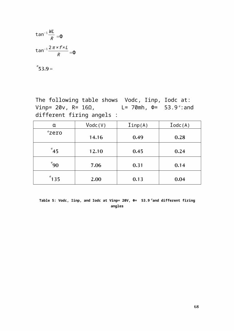
If R= 16Ω and L= 70mh then the load angle can be calculated as a following:
Ф =tan−1 WLR
Ф =tan−1 2 π × f × LR
= 53.9°
The following table shows Vodc, Iinp, Iodc at: Vinp= 20v, R= 16Ω, L= 70mh, Ф= 53.9°:and different firing angels :
α Vodc(V) Iinp(A) Iodc(A)zero° 14.16 0.49 0.2845° 12.10 0.45 0.2490° 7.06 0.31 0.14135° 2.00 0.13 0.04
Table 5: Vodc, Iinp, and Iodc at Vinp= 20V, Ф= 53.9°and different firing angles
54

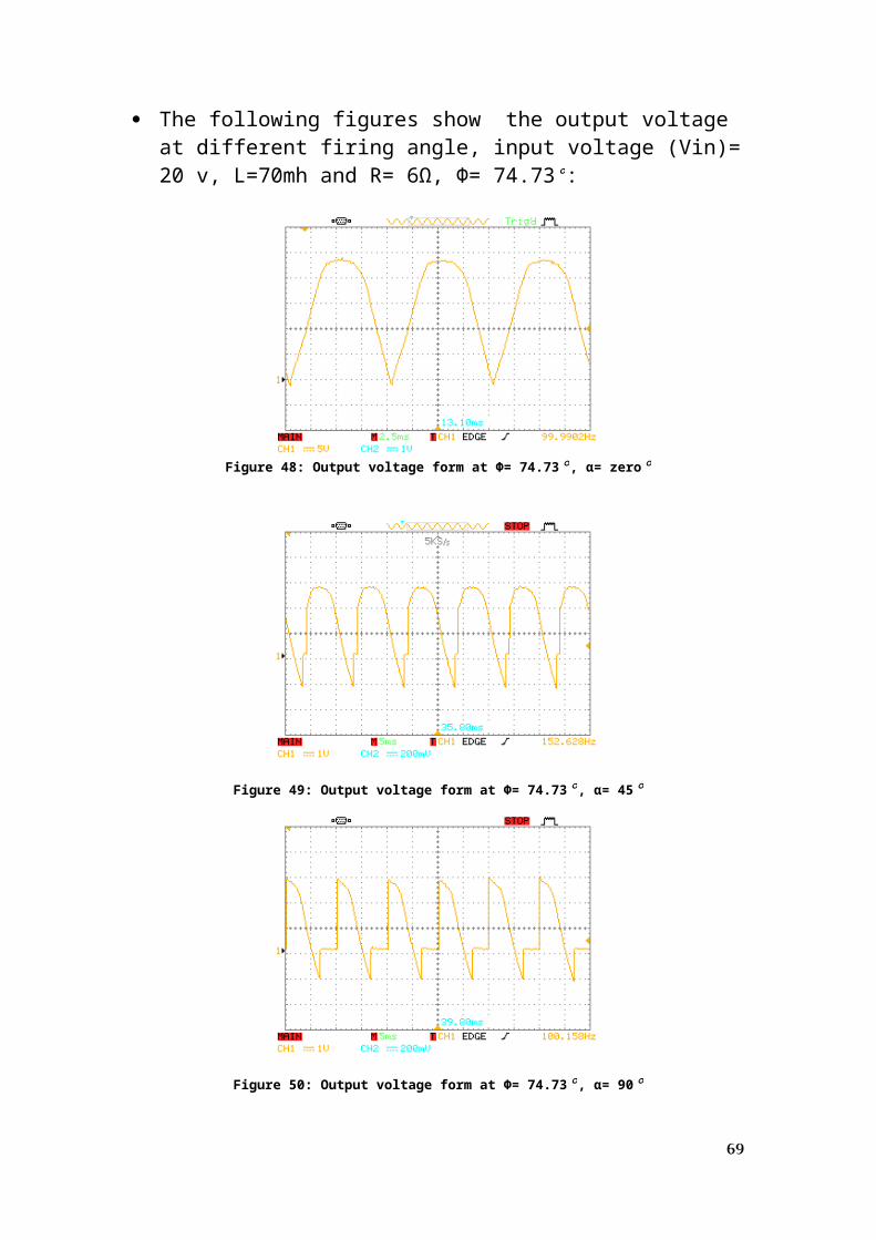
The following figures show the output voltage at different firing angle, input voltage (Vin)= 20 v, L=70mh and R= 6Ω, Ф= 74.73°:
Figure 48: Output voltage form at Ф= 74.73°, α= zero°
Figure 49: Output voltage form at Ф= 74.73°, α= 45°
Figure 50: Output voltage form at Ф= 74.73°, α= 90°
55

Figure 51: Output voltage form at Ф= 74.73°, α= 135°
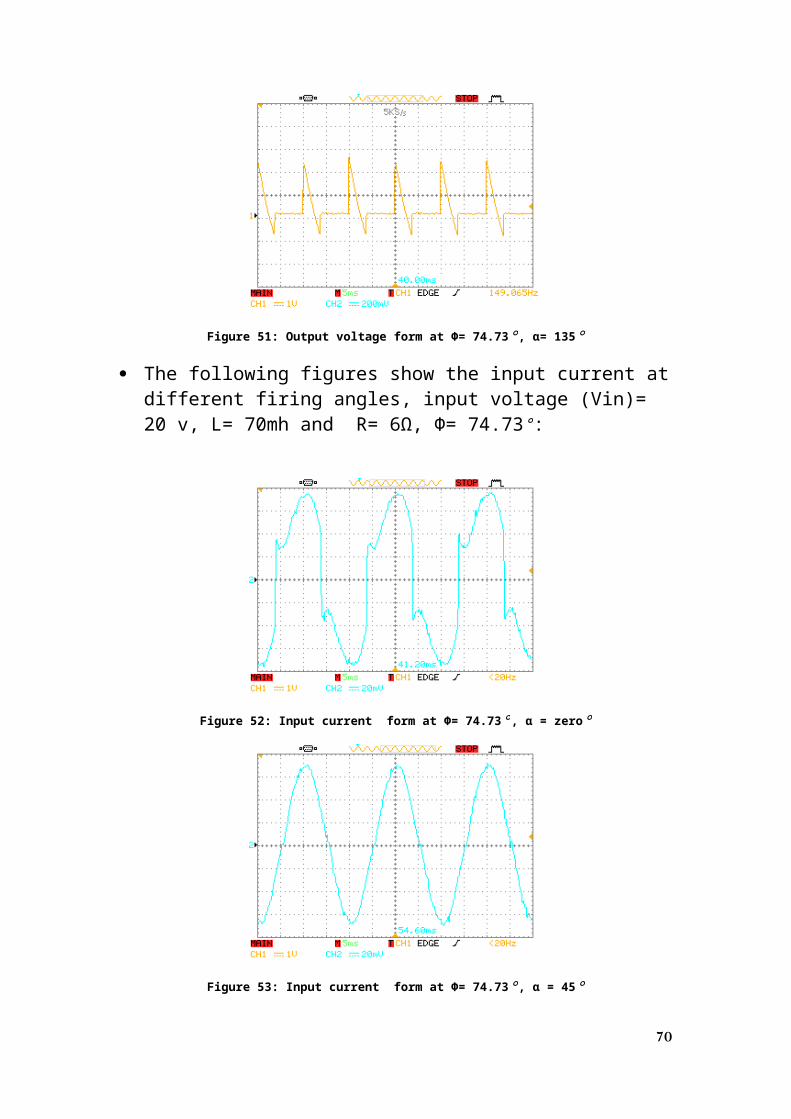
The following figures show the input current at different firing angles, input voltage (Vin)= 20 v, L= 70mh and R= 6Ω, Ф= 74.73°:
Figure 52: Input current form at Ф= 74.73°, α = zero°
Figure 53: Input current form at Ф= 74.73°, α = 45°
56

Figure 54: Input current form at Ф= 74.73°, α = 90°
Figure 55: Input current form at Ф= 74.73°, α = 135°
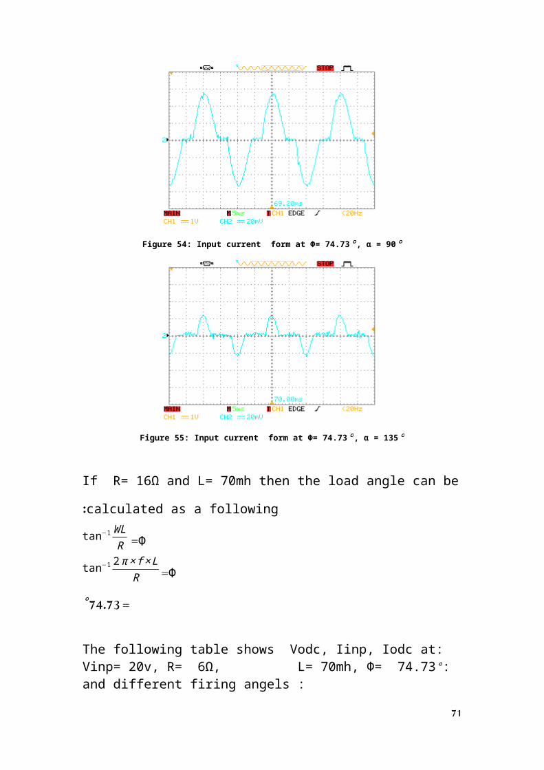
If R= 16Ω and L= 70mh then the load angle can be calculated as a following:
Ф =tan−1 WLR
Ф =tan−1 2 π × f × LR
= 74.73°
The following table shows Vodc, Iinp, Iodc at: Vinp= 20v, R= 6Ω, L= 70mh, Ф= 74.73°: and different firing angels :
Α Vodc(V) Iinp(A) Iodc(A)zero° 13.46 0.48 0.3445° 10.59 0.41 0.2690° 5.97 0.28 0.15135° 1.51 0.12 0.037
57

Table 6: Vodc, Iinp, and Iodc at Vinp= 20V, Ф= 74.73°and different firing angles
The following figures show the output voltage at different firing angle, input voltage (Vin)= 20 v, L=241mh and R= 16Ω, Ф= 78.06° :
Figure 56: Output voltage form at Ф= 78.06°, α= zero°
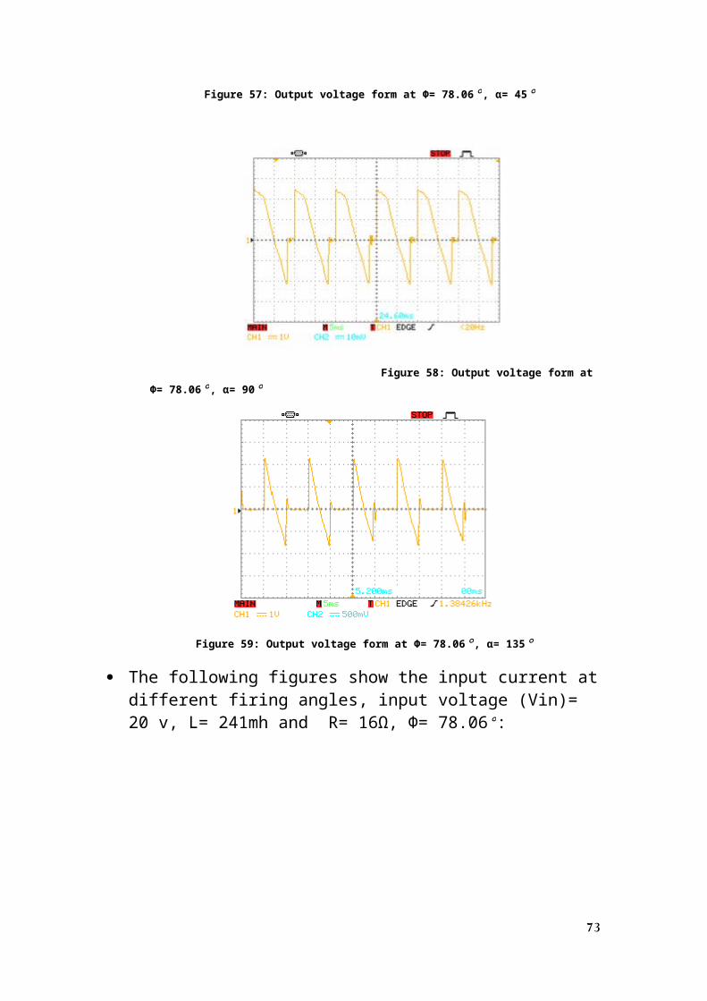
Figure 57: Output voltage form at Ф= 78.06°, α= 45°
58

Figure 58: Output voltage form at Ф= 78.06°, α= 90°
Figure 59: Output voltage form at Ф= 78.06°, α= 135°
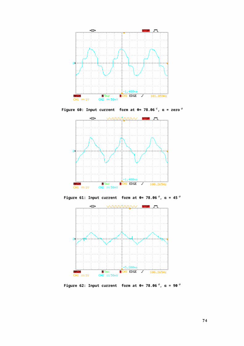
The following figures show the input current at different firing angles, input voltage (Vin)= 20 v, L= 241mh and R= 16Ω, Ф= 78.06°:
Figure 60: Input current form at Ф= 78.06°, α = zero°
59

Figure 61: Input current form at Ф= 78.06°, α = 45°
Figure 62: Input current form at Ф= 78.06°, α = 90°
Figure 63: Input current form at Ф= 78.06°, α = 135°
If R= 16Ω and L= 241mh then the load angle can be calculated as a following:
Ф =tan−1 WLR
Ф =tan−1 2 π × f × LR
= 78.06°
The following table shows Vodc, Iinp, Iodc at: Vinp= 20v, R= 16Ω, L= 241mh, Ф= 78.06° and different firing angels:
Α Vodc(V) Iinp(A) Iodc(A)zero° 13.1 0.52 0.1545° 10.4 0.42 0.1190° 5.1 0.20 0.06135° 0.83 0.06 0.008
60

Table 7: Vodc, Iinp, and Iodc at Vinp= 20V, Ф= 78.06°and different firing angles
The following figures show the output voltage at different firing angle, input voltage (Vin)= 20 v, L=455mh and R= 16Ω, Ф= 83.61°:
Figure 64: Output voltage form at Ф= 83.61°, α= zero°
Figure 65: Output voltage form at Ф= 83.61°, α= 45°
61
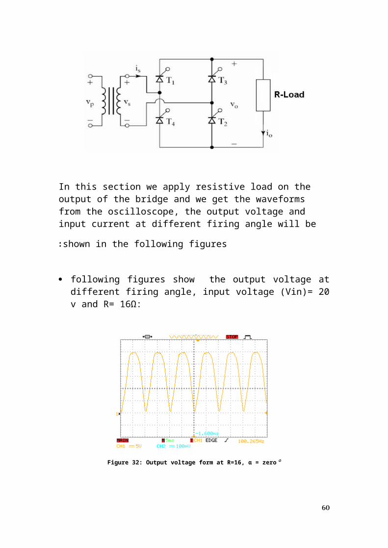
Figure 66: Output voltage form at Ф= 83.61°, α= 90°
Figure 67: Output voltage form at Ф= 83.61°, α= 135°
The following figures show the input current at different firing angles, input voltage (Vin)= 20 v, L= 455 mh and R= 16Ω, Ф= 83.61°:
Figure 68: Input current form at Ф= 83.61°, α = zero°
62
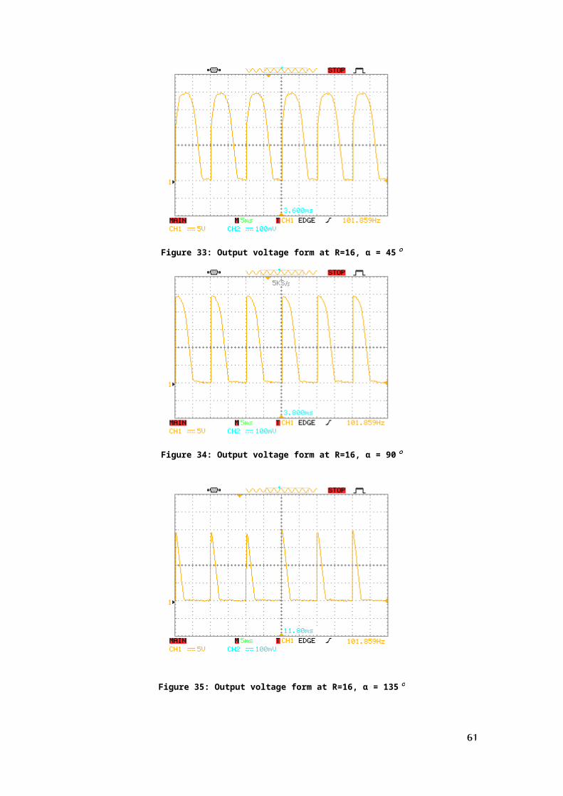
Figure 69: Input current form at Ф= 83.61°, α = 45°
Figure 70: Input current form at Ф= 83.61°, α = 90°
Figure 71: Input current form at Ф= 83.61°, α = 135°
If R= 16Ω and L= 455mh then the load angle can be calculated as a following:
Ф =tan−1 WLR
63
Ф =tan−1 2 π × f × LR
= Ф= 83.61°
The following table shows Vodc, Iinp, Iodc at: Vinp= 22v, R= 16Ω, L= 455mh, Ф= 83.61°:and different firing angels :
Α Vodc(V) Iinp(A) Iodc(A)zero° 12.30 0.2 0.08245° 10.16 0.16 0.06790° 3.7 0.09 0.024135° 0.80 0.05 0.005
Table 8: Vodc, Iinp, and Iodc at Vinp= 20V, Ф= 83.61°and different firing angles
4.3: DC motor speed control:
The single phase bridge also can be used to control the speed of DC motor by changing the value of output voltages and this can be achieved by changing the firing angel.
The following diagram shows the equivalent circuit of the DC motor connected to the single phase bridge :
Figure 72: equivalent circuit of the DC motor connected to the single phase bridge
can be noted that the equivalent circuit of the DC motor consist of resistor, inductor and battery, the battery affects the form of output and input current. This deference is shown in the following figures:
64
The following figures show the output voltage of DC motor:
Figure 73: output voltage of DC motor at α= zero°
Figure 74: output voltage of DC motor at α= 45°
Figure 75: output voltage of DC motor at α= 90°
65
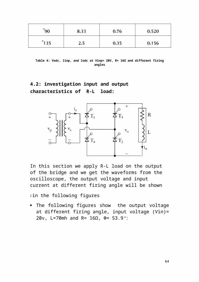
Figure 76: output voltage of DC motor at α= zero°
The following figures show the input current of DC motor:
Figure 77: the input current of DC motor α = zero°
66
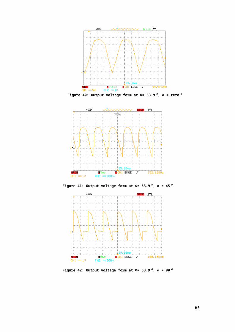
Figure 78: the input current of DC motor α =45°
Figure 79: the input current of DC motor α = 90°
Figure 80: the input current of DC motor α =135°
67
From these figures we can notice that the value of the output voltage and the speed of DC motor increase as we reduce the firing angel and , and this method could be used to control the speed of DC motor in different appliances.
4.4 investigation about the improvement of the grid current:From the previous sections we note that the input current of the bridge at different load contains a lot of high harmonics component , this components have very bad effects on AC machines like motors, transformers that connect to the network supply the bridge, also the communication devices around the bridge so, at this section the input current will be improved by using filter on the input side of the rectifier.
The first step at this stage is to analyze the input current by using Fourier analysis as following:
68
Ip(t)= Idc + ∑n=1
∞
an cosnwt+bn sin wnt
Ipdc= 12 π ∫
α
α +π
Iadwt−¿ ∫α+π
α+2 π
Iadwt ¿
= zero.
an= 1π ¿
an= −4 Ianπ sin nα , for n= 1,3,5….
an= zero , for n= 2,4,6…..
bn= 1π ¿
bn= 4 Ianπ cos nα , for n= 1,3,5….
bn= zero , for n= 2,4,6…..
Ip(t)= ∑n=1,3,5. .
∞
√2 In sin(nwt+Ф n)
√2In = √an2+bn2
In= √( 4 Ianπ
sin nα )2
+( 4 Ianπ
cos nα)2
√2
69
In= 4 Ia
√2 nπ
= 2√2 Ianπ
I1= 2√2π Ia
= 0.9 Ia rms value of the fundamental wave (50Hz).
Ip(t) = 4 Iaπ sin (wt−α ) + 4 Ia
3 π sin (3 wt−3 α ) + 4 Ia5 π sin (5 wt−5 α ) …..
Harmonic in power electronic circuit is given by the following equation:
Hi = Kp ∓ 1
K= 1,2,3…
P= pulse number.
In our circuit P=2 so:
Hi = 3,5,7,9….
Fhp = 150,250,350,450…..
To remove these harmonics an LC resonance circuit will be used.
The following figure shows the connection of this circuit to our bridge:
70
The cut off frequency of this circuit is given by the following equation:
f = 12π √LC
at least we want to remove the harmonic which have 350 and 450 Hz so, and from this equation we find the values of capacitors after making the values of inductors and frequencies constant.the following table shows this values:
CfL4813.6 μf350 Hz43 μh
2912 μf450 Hz43 μh207 μf350 Hz1 mh125 μf450 Hz1 mh
121.7 μf350 Hz1.7 mh73.65 μf450 Hz1.7 mh33.3 μf350 Hz6.2 mh20.2 μf450 Hz6.2 mh25.8 μf350 Hz8 mh15.6 μf450 Hz8 mh18.8 μf350 Hz11 mh
11.38 μf450 Hz11 mh3.9 μf350 Hz53 mh2.3 μf450 Hz53 mh
0.41 μf350 Hz500 mh0.25 μf450 Hz500 mh
Table 9: Values for L and C for resonance circuit
71
Practically these values are not available in our market because we need to use non polar capacitor with high capacity and high voltages, also we face problems in finding the suitable value of inductors.
At this stage we use the closest available values of inductors and polar capacitors to achieve this improvement , but the result was in contracts of our expectation and the input current become worst.
After we faille to improve the input current by using the previous circuit, we try to achieve this improvement by using low pass filter circuit .
The following figure shows the connection of this circuit to our bridge:
The cut off frequency of this circuit is given by the following equation:
f = 1RC
the following table shows the values of cut off frequency at specified value of R and C:
Cut off frequencyCR398 Hz400 μf1Ω159 Hz1000 μf1Ω79 Hz2000 μf1Ω53 Hz3000 μf1Ω
Table 10: Values for R,C and cut of frequency for low pass filter
72
The input current waveforms after filtering are shown in the following figures:
Figure 81: The input current waveforms after filtering at Fc= 398 Hz
Figure 82: The input current waveforms after filtering at Fc= 159 Hz
Figure 83: The input current waveforms after filtering at Fc= 79 Hz
73
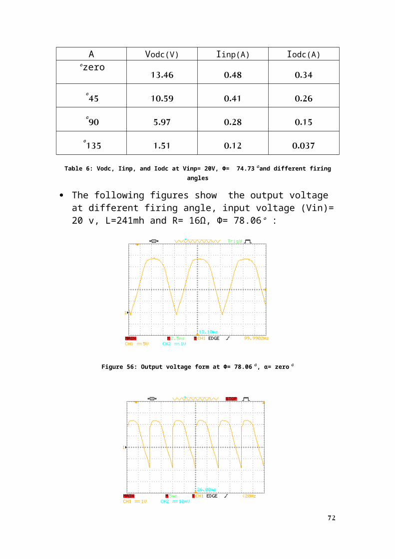
Figure 84: The input current waveforms after filtering at Fc= 53 Hz
Note: applying this type of filtering will produce the same shape of input current whatever the type of the load or the triggering angel because the capacitor block all the high frequencies.
We can notice now that the input current becomes more sinusoidal and more stable as we reduce the cut off frequency and be closer to the fundamental frequency .
74
Chapter five: Discussion and conclusion
In this chapter the benefits, results and application of our project will be discussed, also suggestion of improvements could take place in the future. Applications:
Single phase full wave bridge rectifier controlled by microprocessor has been built, this circuit could be used as: 1- Power electronic lab unit 2- DC motor speed controller 3- Battery charger 4- Part of uninterrupted power system(UPS).
Benefits:
1- Improve our skills in designing electronic circuits and interfaces by using the simple electronic components (resistors, capacitors, transformers and diods), and more complicated components like photo couplers.
2- Learn how to use the measurement devices and how to take accurate measurement by using multimeter and oscilloscope .
3- Have a basic idea about how to use microprocessor (PIC), building its basic and program it successfully.
4- Have a good acknowledgment about the basic power electronics component (thyristor).
5- Understanding the concepts of power electronic like triggering (firing angel), thyristor turn on, thyristor I-V characteristics, load angel, input and output waveforms.
Future suggestions :
1- Varying the firing angle of the thyristor of this circuit by using potentiometer (this need high level of calibration for the thyristor firing angle with the PIC analog to digital by programming ).
2- Using this circuit in industrial application but for huge applications the thyristor should be changed to be more suitable and stand with high currents.
3- Use this circuit to build a complete uninterrupted power system ( UPS) .
75
76