Embed Size (px)
Citation preview
eng_4625_labs_2004.doc 1 4625 Labs Rev E: Boyd Blackwell
ENGN4625 Power Engineering Laboratory: 2004 AC DC (1) DC-DC Motor Drives Power Quality Protection,Fuses Jul31, Aug 7, 14 notes due 19
2nd Sept 6%
Aug 21,8 Sep 4th Report due 912th Sept 11%
Sept 11, Oct 9 notes due 1621th Oct 6% Quiz on 10th
Sept 18 Report due 14th October 9%
16 Oct sheet on day. 3%
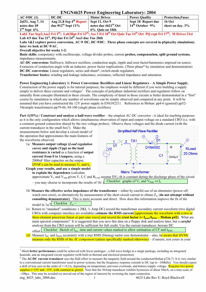
Lab1 Tue Sep2;Ass2 Fri 5th; Lab2Rpt Fri 12th; Ass 3 Fri 10th Oct Quiz Tue 14th Oct PQ rept Fri 17th; M Drives 21st Lab 4/5 due Tue 21st, PQ due Fri 24th Ass3 due Tue 28th Labs 1&2 explore power conversion, AC DC, DC DC. Three phase concepts are covered in pSpice(by simulation). later we look at DC AC. Overall objective list weeks 1-2: Basic skills: competency with oscilloscope, voltage divider probes, current probes, compensation, split ground systems, impedance measurements. AC-DC conversion: Halfwave, fullwave rectifiers, conduction angle, ripple and crest factor/harmonics imposed on source. Extension of conduction angle with an inductor, power factor implications. (Three phase* by simulation and demonstration) DC-DC conversion: Linear regulators, series and shunt*, switch-mode regulators. Transformer basics: winding and leakage inductance, resistance, reflected impedance and saturation. Power Engineering Laboratory 1: Power Conversion: Rectifiers and Linear Regulators – A Simple Power Supply. Construction of the power supply is for tutorial purposes; the emphasis would be different if you were building a supply simply to deliver these currents and voltages1. The concepts of polyphase industrial rectifiers and regulators follow on naturally from concepts illustrated in these circuits. The complexity of detail in those circuits is better demonstrated in a “first” course by simulation in which any number of waveforms can be simply observed and compared at any point. It will be assumed that you have constructed the 12V power supply in ENGN2211. References in Mohan: pp4-6 (general) pp52-54(simple transformers) pp79-86, 94-100 (single phase rectifiers) Part 1(35%) / Construct and analyse a half-wave rectifier – the simplest AC-DC convertor - is ideal for teaching purposes as it is the only configuration which allows simultaneous observation of input and output voltage on a standard CRO (i.e. with a common ground connection shared by the two voltage probes). Observe these voltages and the diode current (with the current transducer in the small box2). Make the measurements below and develop a circuit model of the operation that approximates the main features of the waveforms observed.
1a/ Measure output voltage (Load regulation curve) and ripple (Vpp) as the load resistance is varied as a function of output current from 0 to 1Ampere, using a 2000uF filter capacitor on the output. DVM’s can be used to measure VL and IL.
Graph your results, and use a simple model to explain the dependence (calculate approximate VL and Vripp given V, f, C and RLoad, assume DVC/dt is constant during the discharge phase of the circuit
– you may choose to incorporate the results of 1b/.)
1b/ Measure the effective series impedance of the transformer – either by careful use of an ohmmeter (power off, watch zero error), or alternatively by measurement of the short circuit current to obtain Zsc (do not attempt without consulting demonstrator). This is more accurate and direct. How does this information improve the fit of the
model in 1a/? 1c/ Return to “standard” conditions: ( 20Ω, ½ Amp DC) record the transformer secondary current waveform (two digital
CROs with computer interface are available) estimate the RMS current [approximate the waveform with a two or three element piecewise linear or part sine wave] and record the crest factor (= Ipeak/IRMS – Mohan p42). What are main spectral components? It is suggested that you save this data on a floppy disk and analyse later, but a careful analysis from the CRO screen will be sufficient for full credit. Use the current transducer, beware DC
offset. 1d/ Measure IDC and IRMS accurately with a true RMS (Hameg) meter (see demonstrator – also, be aware that DVMs
measure only the RMS of the AC component (unless specifically marked otherwise) – if unsure, test yours in your
1 Much better performance could be achieved with fewer packages - a full wave bridge in a single package, including an integrated heatsink, and an integrated circuit regulator (with built-in thermal and electrical protection) 2 The AC/DC current transducer uses the Hall effect to measure the magnetic field around the conductor(Mohan p726,7) It is very similar to a conventional current transformer used in power systems, but the frequency response extends to DC (up to ~100kHz). You should expect a drift of true zero in the order of +/-0.2A, depending on temperature, previous overloads, and battery/supply voltage. Requires two power supplies (+15V and –15V, with common to green). Note that the 50Amp transducer exhibits hysteresis of about 50mA, on a time scale of ~100µs. This may be avoided (or moved out of the region of interest) by reversing the input connection
Checklist: Sketch of Isec, time and current values marked to allow estimation of CF and IRMS
Checklist: Zsc =
Checklist: graphs of VL and VRipp vs IL
+
2000µF
eng_4625_labs_2004.doc 2 4625 Labs Rev E: Boyd Blackwell
output load circuit which provides you with a known DC current) and compare with your estimate, then calculate the dissipation in the diode rectifier (using a linear3 or exponential model for the diodes – for a linear model, Vd = Vo+ IdRd, power = VDIDC + Rd × IRMS
2, assume VD ~0.7V, and the transformer secondary(assuming its resistance is the same as at DC). The RMS method requires the use of the linear diode model. To use the exponential diode model, you must either digitize the waveforms, or approximate them, typically by a partial sine wave (parts 1&2) or a
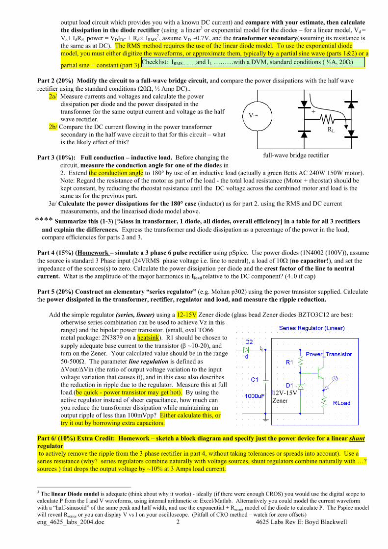
partial sine + constant (part 3). Part 2 (20%) Modify the circuit to a full-wave bridge circuit, and compare the power dissipations with the half wave rectifier using the standard conditions (20Ω, ½ Amp DC)..
2a/ Measure currents and voltages and calculate the power dissipation per diode and the power dissipated in the transformer for the same output current and voltage as the half wave rectifier.
2b/ Compare the DC current flowing in the power transformer secondary in the half wave circuit to that for this circuit – what is the likely effect of this?
Part 3 (10%): Full conduction – inductive load. Before changing the
circuit, measure the conduction angle for one of the diodes in 2. Extend the conduction angle to 180° by use of an inductive load (actually a green Betts AC 240W 150W motor). Note: Regard the resistance of the motor as part of the load - the total load resistance (Motor + rheostat) should be kept constant, by reducing the rheostat resistance until the DC voltage across the combined motor and load is the same as for the previous part.
3a/ Calculate the power dissipations for the 180° case (inductor) as for part 2. using the RMS and DC current measurements, and the linearised diode model above.
**** Summarize this (1-3) [%loss in transformer, 1 diode, all diodes, overall efficiency] in a table for all 3 rectifiers and explain the differences. Express the transformer and diode dissipation as a percentage of the power in the load, compare efficiencies for parts 2 and 3.
Part 4 (15%) (Homework – simulate a 3 phase 6 pulse rectifier using pSpice. Use power diodes (1N4002 (100V)), assume the source is standard 3 Phase input (24VRMS phase voltage i.e. line to neutral), a load of 10Ω (no capacitor!), and set the impedance of the sources(s) to zero. Calculate the power dissipation per diode and the crest factor of the line to neutral current. What is the amplitude of the major harmonics in Iload relative to the DC component? (4..0 if cap) Part 5 (20%) Construct an elementary “series regulator” (e.g. Mohan p302) using the power transistor supplied. Calculate the power dissipated in the transformer, rectifier, regulator and load, and measure the ripple reduction.
Add the simple regulator (series, linear) using a 12-15V Zener diode (glass bead Zener diodes BZTO3C12 are best: otherwise series combination can be used to achieve Vz in this range) and the bipolar power transistor. (small, oval TO66 metal package: 2N3879 on a heatsink). R1 should be chosen to supply adequate base current to the transistor (β ~10-20), and turn on the Zener. Your calculated value should be in the range 50-500Ω. The parameter line regulation is defined as ∆Vout/∆Vin (the ratio of output voltage variation to the input voltage variation that causes it), and in this case also describes the reduction in ripple due to the regulator. Measure this at full load.(be quick - power transistor may get hot). By using the active regulator instead of sheer capacitance, how much can you reduce the transformer dissipation while maintaining an output ripple of less than 100mVpp? Either calculate this, or try it out by borrowing extra capacitors.
Part 6/ (10%) Extra Credit: Homework – sketch a block diagram and specify just the power device for a linear shunt regulator to actively remove the ripple from the 3 phase rectifier in part 4, without taking tolerances or spreads into account). Use a series resistance (why? series regulators combine naturally with voltage sources, shunt regulators combine naturally with …? sources ) that drops the output voltage by ~10% at 3 Amps load current. 3 The linear Diode model is adequate (think about why it works) - ideally (if there were enough CROS) you would use the digital scope to calculate P from the I and V waveforms, using internal arithmetic or Excel/Matlab. Alternatively you could model the current waveform with a “half-sinusoid” of the same peak and half width, and use the exponential + Rseries model of the diode to calculate P. The Pspice model will reveal Rseries or you can display V vs I on your oscilloscope. (Pitfall of CRO method – watch for zero offsets)
Checklist: IRMS…… …and IL ………with a DVM, standard conditions ( ½A, 20Ω)
12V-15V Zener
full-wave bridge rectifier
V~RL
+

eng_4625_labs_2004.doc 3 4625 Labs Rev E: Boyd Blackwell
Required Components: 24Vac transformer(largeGreen Box “Betts” 24V10Amp supply), 4 ea 1Amp power diodes, 1-4 × 1000µF electrolytic, 20-100Ω 100W rheostat, 2N3879 on Heatsink***, 15-20V 0.5Watt Zener (put two in series to achieve V and P). DC Current transducer*** *** not in self service boxes
Laboratory Reports Two reports are to be written up “formally”. The rest are either lab. notebook style, or sheets to be filled in. Formal reports Length: Maximum 7 pages 12pt type. If Graphs and figures are attached separately, they count as 1/3 page each graph/figure. Figures: No requirement or extra marks for computer drawn graphs/figures, but in either form, they must be reasonably neat. Content: Abstract, introduction and conclusion should be brief and to the point. Good presentation, analysis and discussion of results is more important. Numbering: Use the lab handout numbering to make it clear which part you are answering, Most frequent loss of marks is omission of a part of the work. I recommend that you show me your report when it is close to completion, to check for glaring errors.
eng_4625_labs_2004.doc 4 4625 Labs Rev E: Boyd Blackwell
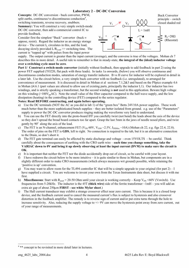
Laboratory 2 – DC-DC Conversion Concepts: DC-DC conversion - buck convertor, PWM, split earths, continuous/vs discontinuous conduction4, switching transients, reverse recovery, snubbers. Summary: You will construct a very simple switch-mode DC-DC converter, then add a commercial control IC to provide feedback. Consider first the simplest “Buck” convertor (buck ≡ oppose, resist). Regard the inductor as an energy storage device – The current IL circulates in this, and the load, decaying slowly provided L/RLoad >> switching time. The current is “topped up” with pulses from the input power supply. The output current is greater than the input current (average), and the converse is true of the voltages. Mohan ch 7 describes this in more detail. A useful rule to remember is that in steady-state, the integral of the (ideal) inductor voltage over a switching cycle must be zero. Part 1/ Construct a switch-mode convertor (initially without feedback, then upgrade to add feedback in part 2) using the power FET supplied (TO220, flat pack with three leads). In tasks 1a onwards, (below) you will observe continuous and discontinuous conduction modes, saturation of energy transfer inductor. B vs H curve for inductor will be explored in detail in a later lab. Use the circuit below, a very simple buck convertor with no feedback (i.e. unregulated), re-arranged for convenience of measurement. It is discussed in detail in Mohan et al sections 7.1,2&3 and based on the PSpice example 4.6 in Mohan §4.6.1 (part values are altered to allow use of existing parts, principally the inductor L1). Our inductor has two windings, and is strictly speaking a transformer, but the second winding is not used in this application. Beware high voltage on this winding (>100VppAC). Note the small value of the filter capacitor compared to the half-wave supply, and the low dissipation (heating) in the controlling device (FET) compared to the series regulator. Notes: Read BEFORE constructing, and again before operating. a) Use the DC terminals (NOT the AC as you did in lab 1) of the “green box” Betts 24V10A power supplies. These work
much better than the more sophisticated bench supplies – they are better isolated from ground. e.g. use of the “Parameters” supply to power the DC-DC convertor produces ringing making the waveforms very hard to understand.
b) You can use the FET directly into the proto-board IFF you carefully twist (not bend) the leads about the axis of the device so they don’t spread the bread board contacts too far apart. Grasp the last 5mm in the jaws of needle nosed pliers, and twist gently by 90ο along the axis of the lead.
c) The FET is an N-channel, enhancement FET (VDS 60V, VGS0 ~2.5V, IDSMax ~10A) (Mohan ch 22, e.g. figs 22.4, 22.8). The order of pins on the FET is GDS, left to right. No connection is required to the tab, but it is an alternative connection to the Drain, so don’t short it.
d) The FET gate terminal can easily be affected by static discharge and voltage - even 15VOLTS – be careful. Think carefully about the consequences of earthing with the CRO earth wire – each time you change something, take the VARIAC down to 0V and bring it up slowly observing at least the input current (DVM) to make sure the circuit is OK.
e) It is important that neither the FET nor the diode accidentally drop out of circuit, so be careful with your layout. f) I have redrawn the circuit below to be more intuitive – it is quite similar to those in Mohan, but components are in a
slightly different order to make CRO measurements (which always measures wrt ground) possible, while retaining the ‘positive is up’ convention.
g) You may want to allow room for the TL494 controller IC that will be a simple upgrade to your original (for part 2) – I have supplied a circuit. You are welcome to invent your own from the Texas Instruments data sheet, but discuss it with me first.
h) Miscellaneous: Start with Rsnub = 20-50 Ohm until your circuit is working correctly – Keep VDS <60V (Vswitch). Use frequencies from 5-20kHz. The inductor is the 45T (thick wire) side of the ferrite transformer ~1mH – you will add an extra air gap of about 250µm FIRST - see white Mylar sheet.)
i) The Hall current transducer may exhibit a strange crossover effect near zero current. This is because it is a closed loop device, and the feedback current used to cancel the measured current’s flux is subject to hysteresis and also crossover distortion in the feedback amplifier. The remedy is to reverse sign of current and/or put extra turns through the hole to increase sensitivity. Also, reducing the supply voltage to +/- 9V can move the hysteresis point away from zero current, out of your range of measurements.
4 ** concept to be revisited in more detail later in lectures.
V2
L = 1mH
RL=20Ω(Rheostat)I1 IL
V1
+
Buck Convertorprinciple – switchclosed shaded red
I1
VD
eng_4625_labs_2004.doc 5 4625 Labs Rev E: Boyd Blackwell
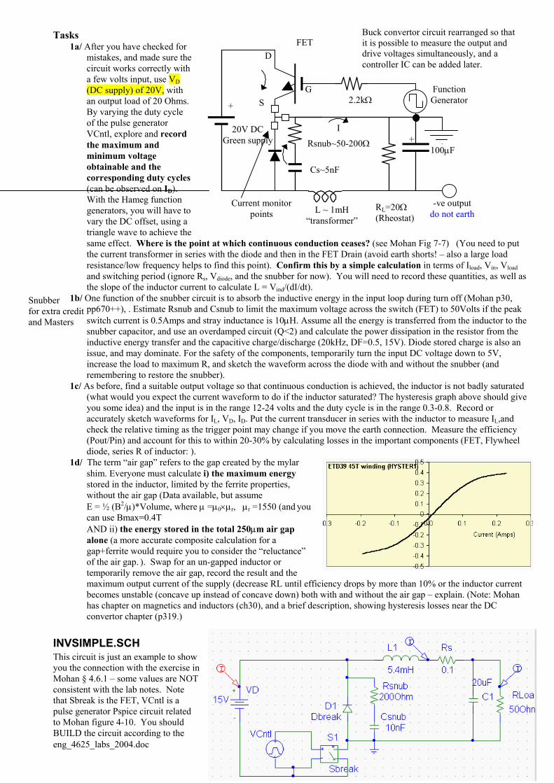
Tasks 1a/ After you have checked for
mistakes, and made sure the circuit works correctly with a few volts input, use VD (DC supply) of 20V, with an output load of 20 Ohms. By varying the duty cycle of the pulse generator VCntl, explore and record the maximum and minimum voltage obtainable and the corresponding duty cycles (can be observed on ID). With the Hameg function generators, you will have to vary the DC offset, using a triangle wave to achieve the same effect. Where is the point at which continuous conduction ceases? (see Mohan Fig 7-7) (You need to put the current transformer in series with the diode and then in the FET Drain (avoid earth shorts! – also a large load resistance/low frequency helps to find this point). Confirm this by a simple calculation in terms of Iload, Vin, Vload and switching period (ignore Rs, Vdiode, and the snubber for now). You will need to record these quantities, as well as the slope of the inductor current to calculate L = Vind/(dI/dt).
1b/ One function of the snubber circuit is to absorb the inductive energy in the input loop during turn off (Mohan p30, pp670++), . Estimate Rsnub and Csnub to limit the maximum voltage across the switch (FET) to 50Volts if the peak switch current is 0.5Amps and stray inductance is 10µH. Assume all the energy is transferred from the inductor to the snubber capacitor, and use an overdamped circuit (Q<2) and calculate the power dissipation in the resistor from the inductive energy transfer and the capacitive charge/discharge (20kHz, DF=0.5, 15V). Diode stored charge is also an issue, and may dominate. For the safety of the components, temporarily turn the input DC voltage down to 5V, increase the load to maximum R, and sketch the waveform across the diode with and without the snubber (and remembering to restore the snubber).
1c/ As before, find a suitable output voltage so that continuous conduction is achieved, the inductor is not badly saturated (what would you expect the current waveform to do if the inductor saturated? The hysteresis graph above should give you some idea) and the input is in the range 12-24 volts and the duty cycle is in the range 0.3-0.8. Record or accurately sketch waveforms for IL, VD, ID. Put the current transducer in series with the inductor to measure IL,and check the relative timing as the trigger point may change if you move the earth connection. Measure the efficiency (Pout/Pin) and account for this to within 20-30% by calculating losses in the important components (FET, Flywheel diode, series R of inductor: ).
1d/ The term “air gap” refers to the gap created by the mylar shim. Everyone must calculate i) the maximum energy stored in the inductor, limited by the ferrite properties, without the air gap (Data available, but assume E = ½ (B2/µ)*Volume, where µ =µ0×µr, µr =1550 (and you can use Bmax=0.4T AND ii) the energy stored in the total 250µm air gap alone (a more accurate composite calculation for a gap+ferrite would require you to consider the “reluctance” of the air gap. ). Swap for an un-gapped inductor or temporarily remove the air gap, record the result and the maximum output current of the supply (decrease RL until efficiency drops by more than 10% or the inductor current becomes unstable (concave up instead of concave down) both with and without the air gap – explain. (Note: Mohan has chapter on magnetics and inductors (ch30), and a brief description, showing hysteresis losses near the DC convertor chapter (p319.)
INVSIMPLE.SCH This circuit is just an example to show you the connection with the exercise in Mohan § 4.6.1 – some values are NOT consistent with the lab notes. Note that Sbreak is the FET, VCntl is a pulse generator Pspice circuit related to Mohan figure 4-10. You should BUILD the circuit according to the
FET
RL=20Ω(Rheostat)
I20V DCGreen supply
-ve outputdo not earth
100µF
L ~ 1mH“transformer”
Cs~5nF
Rsnub~50-200Ω
2.2kΩ
Current monitorpoints
+
G
D
S
+
Buck convertor circuit rearranged so thatit is possible to measure the output anddrive voltages simultaneously, and acontroller IC can be added later.
FunctionGenerator
Snubber for extra credit and Masters
eng_4625_labs_2004.doc 6 4625 Labs Rev E: Boyd Blackwell
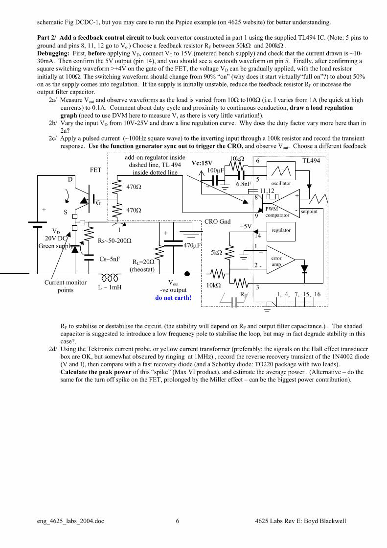
schematic Fig DCDC-1, but you may care to run the Pspice example (on 4625 website) for better understanding. Part 2/ Add a feedback control circuit to buck convertor constructed in part 1 using the supplied TL494 IC. (Note: 5 pins to ground and pins 8, 11, 12 go to Vc.) Choose a feedback resistor RF between 50kΩ and 200kΩ . Debugging: First, before applying VD, connect VC to 15V (metered bench supply) and check that the current drawn is ~10-30mA. Then confirm the 5V output (pin 14), and you should see a sawtooth waveform on pin 5. Finally, after confirming a square switching waveform >+4V on the gate of the FET, the voltage VD can be gradually applied, with the load resistor initially at 100Ω. The switching waveform should change from 90% “on” (why does it start virtually“full on”?) to about 50% on as the supply comes into regulation. If the supply is initially unstable, reduce the feedback resistor RF or increase the output filter capacitor.
2a/ Measure Vout and observe waveforms as the load is varied from 10Ω to100Ω (i.e. I varies from 1A (be quick at high currents) to 0.1A. Comment about duty cycle and proximity to continuous conduction, draw a load regulation graph (need to use DVM here to measure V, as there is very little variation!).
2b/ Vary the input VD from 10V-25V and draw a line regulation curve. Why does the duty factor vary more here than in 2a?
2c/ Apply a pulsed current (~100Hz square wave) to the inverting input through a 100k resistor and record the transient response. Use the function generator sync out to trigger the CRO, and observe Vout. Choose a different feedback
RF to stabilise or destabilise the circuit. (the stability will depend on RF and output filter capacitance.) . The shaded capacitor is suggested to introduce a low frequency pole to stabilise the loop, but may in fact degrade stability in this case?.
2d/ Using the Tektronix current probe, or yellow current transformer (preferably: the signals on the Hall effect transducer box are OK, but somewhat obscured by ringing at 1MHz) , record the reverse recovery transient of the 1N4002 diode (V and I), then compare with a fast recovery diode (and a Schottky diode: TO220 package with two leads). Calculate the peak power of this “spike” (Max VI product), and estimate the average power . (Alternative – do the same for the turn off spike on the FET, prolonged by the Miller effect – can be the biggest power contribution).
FET
RL=20Ω(rheostat)
IVD20V DC
Green supply
Vout-ve output
do not earth!
470µF
CRO Gnd
L ~ 1mH
Cs~5nF
Rs~50-200Ω
10kΩRF
5kΩ
setpoint
+
-
TL494
+
-
6.8nF
10kΩ 6
5
8
9
141
2
3
oscillator
PWMcomparator
erroramp
11,12
Vc:15V
470Ω
1, 4, 7, 15, 16
regulator+5V
Current monitorpoints
+G
D
S
add-on regulator insidedashed line, TL 494
inside dotted line
+
100µF
+470Ω

eng_4625_labs_2004.doc 7 4625 Labs Rev E: Boyd Blackwell
Part 3/ Model a feedback-controlled “phase controlled rectifier” with pSpice. Specifications: (Some of the specs (V, number of phases) are chosen to allow use of the evaluation/student version of pSpice) Input voltage:– 24V amplitude5, TWO phase (0, 180ο) Output Load: 10Ω
a/ 10% Create a two phase voltage controlled circuit to allow the output to vary between 0.4A and 1A ( 4V and 10V DC). This may be achieved by using a comparator (we will actually use a voltage-controlled voltage source) to create a firing delay α which is controlled by an applied voltage (VC). This can be achieved by connecting the input AC voltage to one comparator input, and the reference voltage of VC to the other. The comparator output can then trigger the SCR, if connected to the gate terminal by a current limiting resistor, say 1kΩ. This is similar to the threshold method as used internally in the IC (TL494) in part 2, but using the input AC source instead of a sawtooth ramp used by the TL494.
Use a series L-R filter to smooth the output, not an RC filter as before. Choose L to make the ripple at full output < 10%p-p (in current). Record output voltage and % ripple (across the load resistor) for both maximum output(1A) , and minimum output (0.4Ampere), noting also the control voltage required. (Ignore switching transients (spikes) in calculating the ripple). Some hints are given below.
Extra credit: b) +10%Replace the control voltage by a feedback amplifier, making sure that the output voltage sampling circuit has enough low pass filtering so that the firing angle does not vary wildly as a result of ripple voltage appearing in the feedback loop. (You will run into the node limit here again with the student edition unless you use a voltage controlled voltage source instead of an op amp). Even this runs into the limit with a 2 resistor low pass filter!) Choose 3 different feedback gains (say 1,10,100) and measure the load regulation by changing the load resistance by 10% and noting the change in output current (averaged to remove ripple). Express your answer in %Ichange/%R change. Alter the feedback parameters (gain up, filter higher in frequency) until the output shows signs of becoming unstable, and describe the final result, and the values chosen.
Notes/Hints: We are interested here in the power electronics and control aspects of the output of this circuit, so we will use a simplified or ‘conceptual’ drive circuit. This technique is used often in simulations, and saves getting bogged down in detail, and avoids running into the limits of student pSpice. Instead of a real comparator to determine switching times, we can use a “voltage controlled voltage source”, which has a lower component count, requires no external power, its output is electrically isolated from the input, and it behaves ideally. 1. To obtain the maximum control range, the sine wave applied to the comparator would normally be delayed, but that is not
required in this problem (that is why I specified a minimum of 0.4Amp/4V, corresponding to not quite fully phased back. Therefore, if you do not use a delay, achieving the lower limit of current will require a control voltage quite close to the input amplitude, because the switching occurs quite close to the peak of the sine wave.
2. Use two VSIN sources phased to give 180 degrees phase difference. SCR’s 2N1595 can be used. The comparator should be a voltage-controlled voltage source “E” in pSpice. Keep the gain small – 10-100. You can do the compulsory part of this with 11 components: 3R, 1L, 2SCR, 2VSIN 2E, 1V.
3. You should keep the output circuit in continuous conduction mode by choice of suitably large L, otherwise you may have trouble in achieving the lower limit of current.
4. You should organise the circuit so that the same control or threshold voltage VC can be used for both phases. As noted above, the advantage of the voltage-controlled voltage source is that the input and output circuits are isolated.
5. This two-phase circuit is only a small extrapolation from a three or six phase circuit, the one exception being that a two phase circuit can only achieve continuous conduction with an inductive load; three or more phases have overlap between positive half cycles, so continuous conduction can be achieved without the inductor.
6. Don’t worry about switching spikes – you can ‘snub’ them with snubber components, but don’t do this until you are finished adding other components to the circuit, as you may hit the student pSpice limit.
5 The student pSpice SCR is a 50V device, 2N1595. The pSpice model of this device is quite detailed, even in the student version, so if more than 2 are used, the node count limit of pSpice is exceeded. Full versions of pSpice have no trouble with 3 phase or 3 phase six pulse, but to keep things simple, full credit will be given for a 2 phase 2 pulse system, for those not using the full version (most).
New concept: Phase controlled rectifiers (Mohan p121, §2.3 of Basic Switching circuits (KAWalshe) ) are a combination of rectifier and switch mode regulator. This scheme is usually implemented using silicon controlled rectifiers (SCR) otherwise known as thyristors. This is the most common scheme for power conversion in existing equipment and remains the most rugged and powerful option for new designs.

eng_4625_labs_2004.doc 8 4625 Labs Rev E: Boyd Blackwell
See also http://wwwrsphysse.anu.edu.au/~bdb112/engn4625
Power Quality Laboratory Aim: Investigate the effect of various loads on the mains power system by examining the current drawn. The load is typically non-linear, generating Fourier components other than 50Hz, and is time-varying. Power quality criteria applicable to a load include power factor (note full definition below) , generation of harmonics and noise, and voltage dips. Warning! 1/ This lab is only to be performed in the physical presence of Boyd Blackwell or Keith Walshe. Violators will get zero marks and worse! 2/ NEVER connect to the mains except using approved plugs – the voltage is lethal (240V)! The plugpack voltage transformer and the “extension lead with current transformer” are the only connections you should make. Duration 3 hrs max. in lab Writeup – “full report”, including computer processed waveforms. Maximum of 7 equivalent 12pt pages including figures. (full page diagrams count as 1/3 page) Test loads: choose in advance (by email) A/ Computer monitor - observe in standby mode and at full power. B/ 80Watt Fluorescent industrial light assembly – Power factor correction is switchable – observe with and without PF Corr. (Mohan p453, Fluro article on PQT website) C/ Induction motor start up, PF variation with load using the Eddy-Current Dynamometer. (Betts motor, 150W/1500RPM, 240VAC) (Mohan ch14, KAW notes and Cogdell ch. 17) D/ Electric drill (Read up on SCR/Triac phase controllers). Waveforms at low and high speed, and transient at start up. (Loads below (E&F) can be operated successfully from low voltage AC (24V green supply), and the usual CRO probes and Hall current transducer should be used) E&F/ TRIAC phase controlled light dimmer (to be connected to the large load rheostat ONLY at 28V – this provides a current large enough to observe clearly: Note DO NOT CONNECT THE BARE WIRES TO MAINS) ( measurements as for D). Note that you should think about how the device works as you make the observations, and you will formally write about this in part 5.
Measuring Equipment The plugpacks are voltage transformers (VTs) with a ratio 20:1. They are trimmed by a resistive divider (1.91kΩ:12.1kΩ) to be within 1% of that ratio, and they have a very small effect on phase (~3-5°, which is largely compensated by a similar shift in the CTs) The current transformers (CTs) are mounted on a very short extension lead to avoid access to mains wiring. Their calibration is fine-tuned by a resistor (~124Ω±1%) to be 10A/Volt, with a phase shift (at 50Hz) of 3-5°. (As supplied, they are calibrated 4V≡5Amp, intended to be mounted in a PLC or relay-based control system. The small resistor increases their L/R time thereby reducing the phase shift from the ~7° as supplied.) The oscilloscopes (CROs) can calculate Fourier Spectra and instantaneous power (Math function Ch1× Ch2) and average this (“quick measure” function). It is convenient to enter the probe sensitivities so that the units displayed are meaningful.

eng_4625_labs_2004.doc 9 4625 Labs Rev E: Boyd Blackwell
Notes: The Agilent CROs record screen images (TIFFs) and data (CSV) separately. If you want to analyse the data further (say with excel or matlab), then be sure you get both forms. Because only 2000 points of data are saved to disk, be sure you choose them well (ideally 2 cycles, if you don’t plan to use windowing (make sure that you have passed exactly two cycles to the FT routine), or 6-10 cycles if you plan to window the data in the FT step (so that you don’t need to worry about the exact number of cycles). Hold any button down to see ‘help’. The Fluke CROS record also record images and data separately, but there data files are not limited to 2000 points, and can be easily re-displayed as a screen image if a real screen image is not available. The downside of these is the screens are more “dotty”, and the interface is less like a normal CRO than the Agilent. The Agilent CROS record directly to floppy, The Flukes need to be read out into Boyd’s laptop, then copied to floppy. Make sure you have .CSV data files unless you have access to FlukeView software.

eng_4625_labs_2004.doc 10 4625 Labs Rev E: Boyd Blackwell
Tasks 0/ Become familiar with the Fourier transform feature of the CRO using a function generator. In particular, be sure you can relate the RMS measured from the time trace with the harmonic component measurements from the spectrum of a sinusoid. 1/ Obtain a voltage trace AND the spectrum of the voltage using the digital CRO and voltage transformer (VT). Consider only harmonics above 1% of the fundamental amplitude, and check that your settings are OK, by confirming that the ratios of two low order harmonics at two different time base settings remain the same. You should use either an exact integral number of cycles, or use a smoothly (i.e. non-rectangular) windowed sample of 10-20 cycles – otherwise the sampling window will create sidebands which will interfere with other peaks. Record the harmonic amplitudes, and calculate the total relative power in harmonics. This step is necessary because the incoming mains is not ideal. You will interpret these spectra in part 5. You fill in the shaded cells by calculation. Harmonic dB RMS voltage(V) Power rel. to fund. Repeat for the CURRENT drawn by your load. (both trace and spectrum) . This is the crux of the observation. You may need to ignore harmonics less than 3% of the fundamental as there is likely to be a richer spectrum here. Harmonic dB RMS Current(A) Power rel. to fund. 2/ Power factor.
“Phase Lag”
IRMS I1 VRMS P Avg
DPF (cos φ)
PF Mohan
PF (CRO)
P Peak
P min
Comment
“normal”
“other” We wish to quantify the efficiency of this load – a load that takes high peak currents is less efficient (e.g. it causes more heating in the distribution wiring, transformers etc) than one that draws a steady current (analogous to simple power factor for simple sine wave excitation. Mohan defines the generalised power factor
PF = IS1/IS × DPF where DPF (displacement power factor, refers to displacement in time) is the linear power factor (cosφ) and IS1/IS is the ratio of the fundamental RMS current to the whole RMS current. (This is in effect the RMS current drawn by the actual load)/(RMS current required to transfer the same power if the load was ideal and resistive). As a first cut, record the phase shift of the current w.r.t voltage, but this is only rough for non-sinusoidal waveforms. The formal power factor is obtained approximately (assuming V is sinusoidal) by measuring PAverage/( IRMSVRMS). Record these raw quantities in the table ( phase lag, IRMS VRMS and PAaverage). For completeness, also record I1 (fundamental RMS) and the peak and trough (may be negative) of the instantaneous power. 3/ Document and discuss variations in power factor generally, and in particular with phase angle (D,E&F), with load (C, E&F) and with PF correction (B). For A, consider the effectiveness of standby mode. 4/ Document (record V and I traces) and discuss start up transients. When there is both in ‘inrush’ and an acceleration transient (e.g. motor, drill) discuss both. Is the startup transient an issue for this device? e.g. does it lower the mains voltage by more than a few percent? 5/ In each case deduce the contents of the electronic box from the current waveforms. Explain what particular features of the waveform influenced your reasoning. Did the waveform vary with time, if so why and what does the variation tell you about the load. (you can refer to the answer for 4 after a brief statement, rather than repeating the detail). 5b/ Discuss the relative DC, 2nd, 3rd, 4th and 5th harmonic current amplitudes (c.f. fundamental) in relation to the assumed electronic circuit, and Mohan Table 18-2 for ISC/I1 < 20. (Note: the DC component is not too obvious, as these probes are AC only.) 6/ What improvements could be made to the power quality of your device, and by what means?
eng_4625_labs_2004.doc 11 4625 Labs Rev E: Boyd Blackwell
Protection devices: Lab 4 (3Hrs) Current Protection
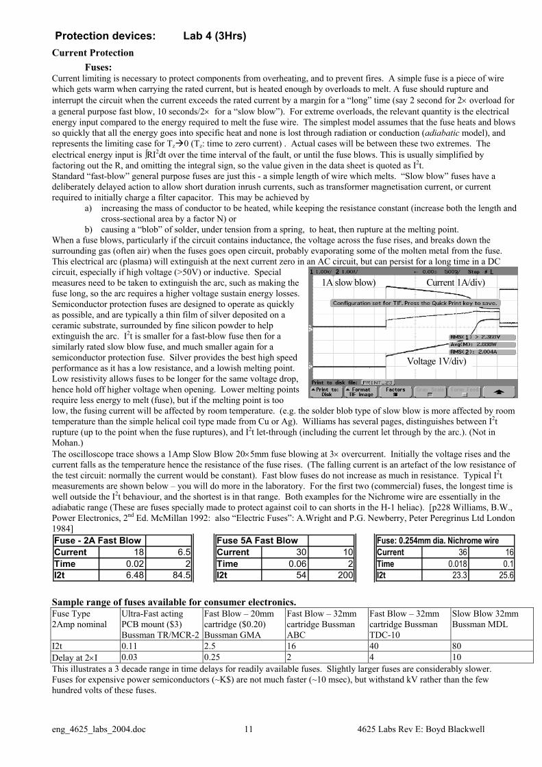
Fuses: Current limiting is necessary to protect components from overheating, and to prevent fires. A simple fuse is a piece of wire which gets warm when carrying the rated current, but is heated enough by overloads to melt. A fuse should rupture and interrupt the circuit when the current exceeds the rated current by a margin for a “long” time (say 2 second for 2× overload for a general purpose fast blow, 10 seconds/2× for a “slow blow”). For extreme overloads, the relevant quantity is the electrical energy input compared to the energy required to melt the fuse wire. The simplest model assumes that the fuse heats and blows so quickly that all the energy goes into specific heat and none is lost through radiation or conduction (adiabatic model), and represents the limiting case for Tz 0 (Tz: time to zero current) . Actual cases will be between these two extremes. The electrical energy input is ∫RI2dt over the time interval of the fault, or until the fuse blows. This is usually simplified by factoring out the R, and omitting the integral sign, so the value given in the data sheet is quoted as I2t. Standard “fast-blow” general purpose fuses are just this - a simple length of wire which melts. “Slow blow” fuses have a deliberately delayed action to allow short duration inrush currents, such as transformer magnetisation current, or current required to initially charge a filter capacitor. This may be achieved by
a) increasing the mass of conductor to be heated, while keeping the resistance constant (increase both the length and cross-sectional area by a factor N) or
b) causing a “blob” of solder, under tension from a spring, to heat, then rupture at the melting point. When a fuse blows, particularly if the circuit contains inductance, the voltage across the fuse rises, and breaks down the surrounding gas (often air) when the fuses goes open circuit, probably evaporating some of the molten metal from the fuse. This electrical arc (plasma) will extinguish at the next current zero in an AC circuit, but can persist for a long time in a DC circuit, especially if high voltage (>50V) or inductive. Special measures need to be taken to extinguish the arc, such as making the fuse long, so the arc requires a higher voltage sustain energy losses. Semiconductor protection fuses are designed to operate as quickly as possible, and are typically a thin film of silver deposited on a ceramic substrate, surrounded by fine silicon powder to help extinguish the arc. I2t is smaller for a fast-blow fuse then for a similarly rated slow blow fuse, and much smaller again for a semiconductor protection fuse. Silver provides the best high speed performance as it has a low resistance, and a lowish melting point. Low resistivity allows fuses to be longer for the same voltage drop, hence hold off higher voltage when opening. Lower melting points require less energy to melt (fuse), but if the melting point is too low, the fusing current will be affected by room temperature. (e.g. the solder blob type of slow blow is more affected by room temperature than the simple helical coil type made from Cu or Ag). Williams has several pages, distinguishes between I2t rupture (up to the point when the fuse ruptures), and I2t let-through (including the current let through by the arc.). (Not in Mohan.) The oscilloscope trace shows a 1Amp Slow Blow 20×5mm fuse blowing at 3× overcurrent. Initially the voltage rises and the current falls as the temperature hence the resistance of the fuse rises. (The falling current is an artefact of the low resistance of the test circuit: normally the current would be constant). Fast blow fuses do not increase as much in resistance. Typical I2t measurements are shown below – you will do more in the laboratory. For the first two (commercial) fuses, the longest time is well outside the I2t behaviour, and the shortest is in that range. Both examples for the Nichrome wire are essentially in the adiabatic range (These are fuses specially made to protect against coil to can shorts in the H-1 heliac). [p228 Williams, B.W., Power Electronics, 2nd Ed. McMillan 1992: also “Electric Fuses”: A.Wright and P.G. Newberry, Peter Peregrinus Ltd London 1984] Fuse - 2A Fast Blow Fuse 5A Fast Blow Fuse: 0.254mm dia. Nichrome wireCurrent 18 6.5 Current 30 10 Current 36 16Time 0.02 2 Time 0.06 2 Time 0.018 0.1I2t 6.48 84.5 I2t 54 200 I2t 23.3 25.6 Sample range of fuses available for consumer electronics. Fuse Type 2Amp nominal
Ultra-Fast acting PCB mount ($3) Bussman TR/MCR-2
Fast Blow – 20mm cartridge ($0.20) Bussman GMA
Fast Blow – 32mm cartridge Bussman ABC
Fast Blow – 32mm cartridge Bussman TDC-10
Slow Blow 32mm Bussman MDL
I2t 0.11 2.5 16 40 80 Delay at 2×I 0.03 0.25 2 4 10 This illustrates a 3 decade range in time delays for readily available fuses. Slightly larger fuses are considerably slower. Fuses for expensive power semiconductors (~K$) are not much faster (~10 msec), but withstand kV rather than the few hundred volts of these fuses.
Voltage 1V/div)
Current 1A/div)1A slow blow)
eng_4625_labs_2004.doc 12 4625 Labs Rev E: Boyd Blackwell
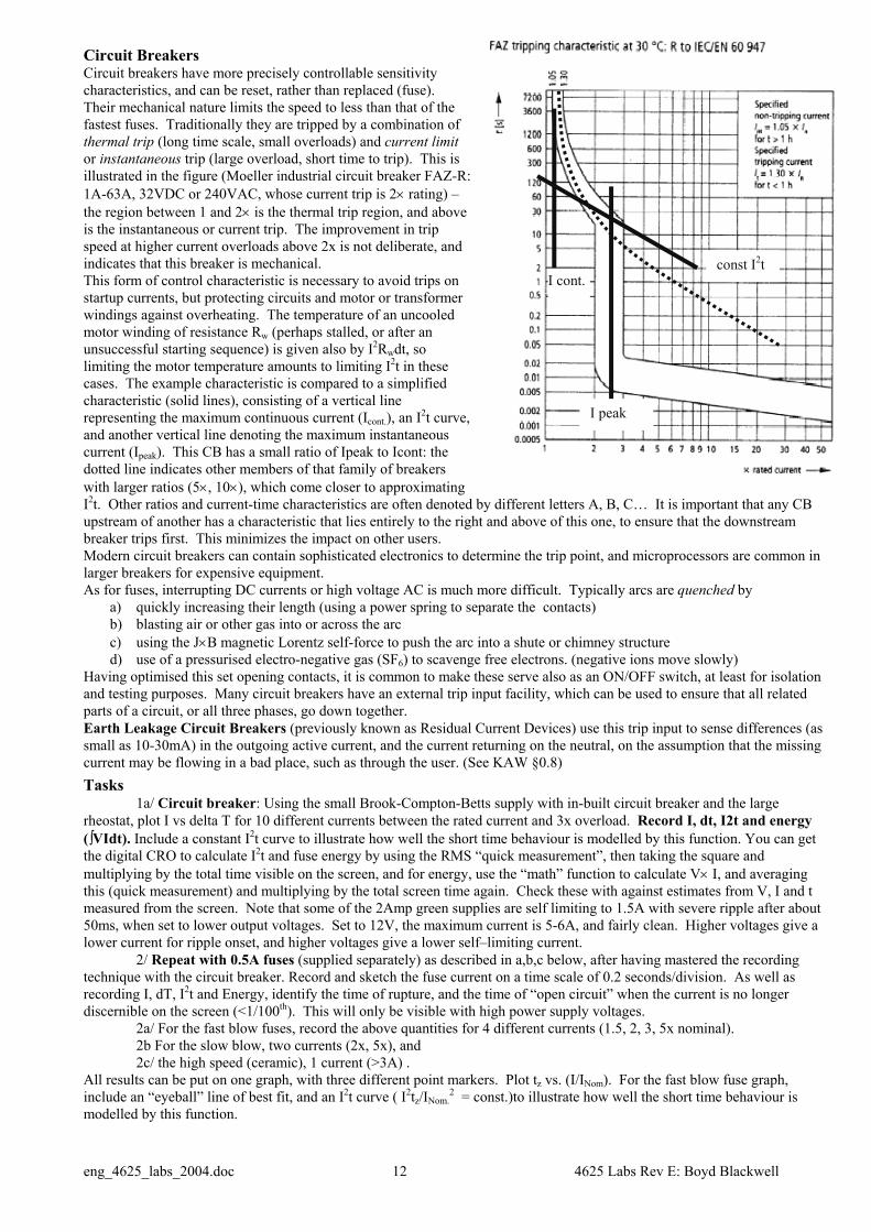
Circuit Breakers Circuit breakers have more precisely controllable sensitivity characteristics, and can be reset, rather than replaced (fuse). Their mechanical nature limits the speed to less than that of the fastest fuses. Traditionally they are tripped by a combination of thermal trip (long time scale, small overloads) and current limit or instantaneous trip (large overload, short time to trip). This is illustrated in the figure (Moeller industrial circuit breaker FAZ-R: 1A-63A, 32VDC or 240VAC, whose current trip is 2× rating) – the region between 1 and 2× is the thermal trip region, and above is the instantaneous or current trip. The improvement in trip speed at higher current overloads above 2x is not deliberate, and indicates that this breaker is mechanical. This form of control characteristic is necessary to avoid trips on startup currents, but protecting circuits and motor or transformer windings against overheating. The temperature of an uncooled motor winding of resistance Rw (perhaps stalled, or after an unsuccessful starting sequence) is given also by I2Rwdt, so limiting the motor temperature amounts to limiting I2t in these cases. The example characteristic is compared to a simplified characteristic (solid lines), consisting of a vertical line representing the maximum continuous current (Icont.), an I2t curve, and another vertical line denoting the maximum instantaneous current (Ipeak). This CB has a small ratio of Ipeak to Icont: the dotted line indicates other members of that family of breakers with larger ratios (5×, 10×), which come closer to approximating I2t. Other ratios and current-time characteristics are often denoted by different letters A, B, C… It is important that any CB upstream of another has a characteristic that lies entirely to the right and above of this one, to ensure that the downstream breaker trips first. This minimizes the impact on other users. Modern circuit breakers can contain sophisticated electronics to determine the trip point, and microprocessors are common in larger breakers for expensive equipment. As for fuses, interrupting DC currents or high voltage AC is much more difficult. Typically arcs are quenched by
a) quickly increasing their length (using a power spring to separate the contacts) b) blasting air or other gas into or across the arc c) using the J×B magnetic Lorentz self-force to push the arc into a shute or chimney structure d) use of a pressurised electro-negative gas (SF6) to scavenge free electrons. (negative ions move slowly)
Having optimised this set opening contacts, it is common to make these serve also as an ON/OFF switch, at least for isolation and testing purposes. Many circuit breakers have an external trip input facility, which can be used to ensure that all related parts of a circuit, or all three phases, go down together. Earth Leakage Circuit Breakers (previously known as Residual Current Devices) use this trip input to sense differences (as small as 10-30mA) in the outgoing active current, and the current returning on the neutral, on the assumption that the missing current may be flowing in a bad place, such as through the user. (See KAW §0.8) Tasks
1a/ Circuit breaker: Using the small Brook-Compton-Betts supply with in-built circuit breaker and the large rheostat, plot I vs delta T for 10 different currents between the rated current and 3x overload. Record I, dt, I2t and energy (∫VIdt). Include a constant I2t curve to illustrate how well the short time behaviour is modelled by this function. You can get the digital CRO to calculate I2t and fuse energy by using the RMS “quick measurement”, then taking the square and multiplying by the total time visible on the screen, and for energy, use the “math” function to calculate V× I, and averaging this (quick measurement) and multiplying by the total screen time again. Check these with against estimates from V, I and t measured from the screen. Note that some of the 2Amp green supplies are self limiting to 1.5A with severe ripple after about 50ms, when set to lower output voltages. Set to 12V, the maximum current is 5-6A, and fairly clean. Higher voltages give a lower current for ripple onset, and higher voltages give a lower self–limiting current.
2/ Repeat with 0.5A fuses (supplied separately) as described in a,b,c below, after having mastered the recording technique with the circuit breaker. Record and sketch the fuse current on a time scale of 0.2 seconds/division. As well as recording I, dT, I2t and Energy, identify the time of rupture, and the time of “open circuit” when the current is no longer discernible on the screen (<1/100th). This will only be visible with high power supply voltages.
2a/ For the fast blow fuses, record the above quantities for 4 different currents (1.5, 2, 3, 5x nominal). 2b For the slow blow, two currents (2x, 5x), and 2c/ the high speed (ceramic), 1 current (>3A) .
All results can be put on one graph, with three different point markers. Plot tz vs. (I/INom). For the fast blow fuse graph, include an “eyeball” line of best fit, and an I2t curve ( I2tz/INom.
2 = const.)to illustrate how well the short time behaviour is modelled by this function.
const I2t
I peak
I cont.
eng_4625_labs_2004.doc 13 4625 Labs Rev E: Boyd Blackwell
Voltage Protection Current limit protection often aims to protect the supply or the supply wiring from overheating, so an opening the faulty circuit is the appropriate action (e.g. fuse). In contrast, most voltage protection (VP) devices act in shunt, as we are protecting the device, not the supply (hence the name “surge divertor”). Also, in many cases, the designer of voltage protection is assuming that there will be an overcurrent protection device somewhere “upstream”, which will trip when the shunt protection activates, as the result of significant increases in the total current. Most VP devices are quite fast (~<µs), so operation time is not the primary concern. Instead, energy absorption and current limits are the most interesting parameters. The Zener or avalanche diode have a very sharp and repeatable turn on, but have the lowest energy and current capability. For varistors, I is approximately described by a power law
I/Io=(V/Vo)α where α is 4-25 (SiC low α, ZnOx+extra high α) A Zener can have an equivalent α as high as 35. (KAW:Motors§2.3.1 uses “b” instead of α). The spark gap offers additional protection in that its “on” voltage drops, reducing the voltage across the protected device. This is how it rates highest in current, although Si-C Varistors rate highest in energy. The spark gap’s two state behaviour can be a problem – it could continue to conduct after the fault is cleared. [KAW: Motors… § 2.3.1Williams p238] Device Timescale Energy limit Current Limit Zener diodes ns low (to 50kW peak power) Moderate Varistors (Metal Oxide) ns high >100A (φ 20mm, pulsed) Varistors (Silicon Carbide) ns highest High Spark Gap µs high Highest
Task 3a/ Compare the V-I characteristic of a Zener diode (the highest voltage you can find), 27V Varistor and 90V spark
gap (actually a “gas discharge tube”). The power law exponent α (“softness or hardness”) of the V-I characteristic may be quantified by taking the ratio of the logs of the current and voltage ratios when the current drops from the maximum attainable to 1/10 of that. Does your measured varistor α value identify its type? This exponent may only be roughly estimated for the non-varistor devices. The difference from the nominal value is simple for the Zener diode; one reading should be sufficient. For the spark gap, take a few readings, and take the worst case error. For the varistor, take the voltage at the maximum current allowed by the curve tracer. Device “Leakage” current at
Vnom*0.9 (Amps) α
log(I2/I1)/ log(V2/V1) Difference from nominal value (%)
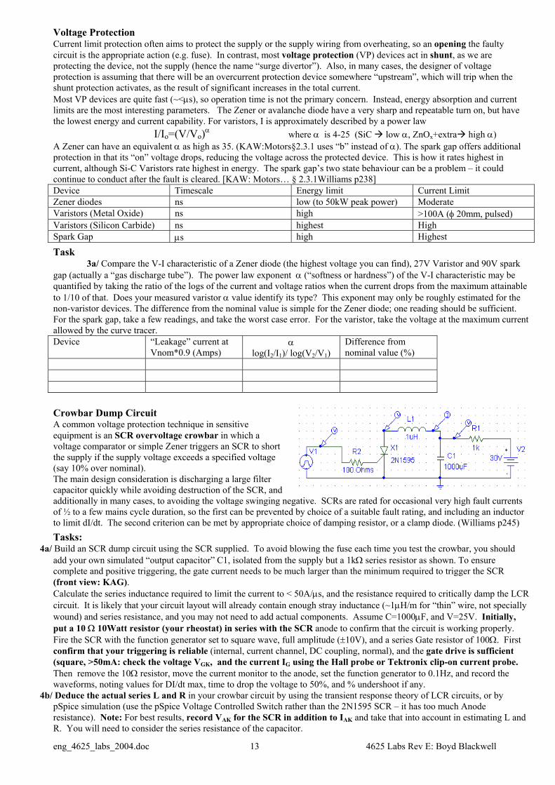
Crowbar Dump Circuit A common voltage protection technique in sensitive equipment is an SCR overvoltage crowbar in which a voltage comparator or simple Zener triggers an SCR to short the supply if the supply voltage exceeds a specified voltage (say 10% over nominal). The main design consideration is discharging a large filter capacitor quickly while avoiding destruction of the SCR, and additionally in many cases, to avoiding the voltage swinging negative. SCRs are rated for occasional very high fault currents of ½ to a few mains cycle duration, so the first can be prevented by choice of a suitable fault rating, and including an inductor to limit dI/dt. The second criterion can be met by appropriate choice of damping resistor, or a clamp diode. (Williams p245) Tasks:
4a/ Build an SCR dump circuit using the SCR supplied. To avoid blowing the fuse each time you test the crowbar, you should add your own simulated “output capacitor” C1, isolated from the supply but a 1kΩ series resistor as shown. To ensure complete and positive triggering, the gate current needs to be much larger than the minimum required to trigger the SCR (front view: KAG). Calculate the series inductance required to limit the current to < 50A/µs, and the resistance required to critically damp the LCR circuit. It is likely that your circuit layout will already contain enough stray inductance (~1µH/m for “thin” wire, not specially wound) and series resistance, and you may not need to add actual components. Assume C=1000µF, and V=25V. Initially, put a 10 Ω 10Watt resistor (your rheostat) in series with the SCR anode to confirm that the circuit is working properly. Fire the SCR with the function generator set to square wave, full amplitude (±10V), and a series Gate resistor of 100Ω. First confirm that your triggering is reliable (internal, current channel, DC coupling, normal), and the gate drive is sufficient (square, >50mA: check the voltage VGK, and the current IG using the Hall probe or Tektronix clip-on current probe. Then remove the 10Ω resistor, move the current monitor to the anode, set the function generator to 0.1Hz, and record the waveforms, noting values for DI/dt max, time to drop the voltage to 50%, and % undershoot if any.
4b/ Deduce the actual series L and R in your crowbar circuit by using the transient response theory of LCR circuits, or by pSpice simulation (use the pSpice Voltage Controlled Switch rather than the 2N1595 SCR – it has too much Anode resistance). Note: For best results, record VAK for the SCR in addition to IAK and take that into account in estimating L and R. You will need to consider the series resistance of the capacitor.
eng_4625_labs_2004.doc 14 4625 Labs Rev E: Boyd Blackwell
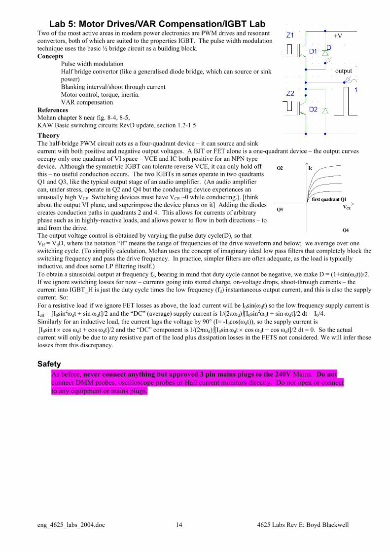
Ic
VCE
first quadrant Q1
Q2
Q3
Q4
Lab 5: Motor Drives/VAR Compensation/IGBT Lab Two of the most active areas in modern power electronics are PWM drives and resonant convertors, both of which are suited to the properties IGBT. The pulse width modulation technique uses the basic ½ bridge circuit as a building block. Concepts
Pulse width modulation Half bridge convertor (like a generalised diode bridge, which can source or sink power) Blanking interval/shoot through current Motor control, torque, inertia. VAR compensation
References Mohan chapter 8 near fig. 8-4, 8-5, KAW Basic switching circuits RevD update, section 1.2-1.5 Theory The half-bridge PWM circuit acts as a four-quadrant device – it can source and sink current with both positive and negative output voltages. A BJT or FET alone is a one-quadrant device – the output curves occupy only one quadrant of VI space – VCE and IC both positive for an NPN type device. Although the symmetric IGBT can tolerate reverse VCE, it can only hold off this – no useful conduction occurs. The two IGBTs in series operate in two quadrants Q1 and Q3, like the typical output stage of an audio amplifier. (An audio amplifier can, under stress, operate in Q2 and Q4 but the conducting device experiences an unusually high VCE. Switching devices must have VCE ~0 while conducting.). [think about the output VI plane, and superimpose the device planes on it] Adding the diodes creates conduction paths in quadrants 2 and 4. This allows for currents of arbitrary phase such as in highly-reactive loads, and allows power to flow in both directions – to and from the drive. The output voltage control is obtained by varying the pulse duty cycle(D), so that Vlf = VdD, where the notation “lf” means the range of frequencies of the drive waveform and below; we average over one switching cycle. (To simplify calculation, Mohan uses the concept of imaginary ideal low pass filters that completely block the switching frequency and pass the drive frequency. In practice, simpler filters are often adequate, as the load is typically inductive, and does some LP filtering itself.) To obtain a sinusoidal output at frequency fd, bearing in mind that duty cycle cannot be negative, we make D = (1+sin(ωdt))/2. If we ignore switching losses for now – currents going into stored charge, on-voltage drops, shoot-through currents – the current into IGBT_H is just the duty cycle times the low frequency (fd) instantaneous output current, and this is also the supply current. So: For a resistive load if we ignore FET losses as above, the load current will be I0sin(ωdt) so the low frequency supply current is Idlf = [I0sin2ωdt + sin ωdt]/2 and the “DC” (average) supply current is 1/(2πωd)∫[I0sin2ωdt + sin ωdt]/2 dt = I0/4. Similarly for an inductive load, the current lags the voltage by 90° (I= -I0cos(ωdt)), so the supply current is [I0sin t × cos ωdt + cos ωdt]/2 and the “DC” component is 1/(2πωd)∫[I0sin ωdt × cos ωdt + cos ωdt]/2 dt = 0. So the actual current will only be due to any resistive part of the load plus dissipation losses in the FETS not considered. We will infer those losses from this discrepancy.
Safety As before, never connect anything but approved 3 pin mains plugs to the 240V Mains. Do not connect DMM probes, oscilloscope probes or Hall current monitors directly. Do not open or connect to any equipment or mains plugs.
+V
output

eng_4625_labs_2004.doc 15 4625 Labs Rev E: Boyd Blackwell
1/ Betts 240V variable speed drive6 The Betts variable speed drive is a properly engineered drive, based on slightly older technology (large high voltage BJTs). You will study it here to observe some of the features that are not implemented the simple IGBT drive you will construct in 2. 1a/ For reference, without the Betts supply, obtain the speed (if available), current (RMS and peak) and average power vs Torque of the Betts 150W Motor using the mains voltage and current monitors, and the Eddy Current Dynamometer for at least five different values of Torque. What is the maximum torque obtainable before the motor starts slipping cycles (“cogging”)? Torque (no
coupler) 0
Speed IRMS IPeak Real Power 1b/ Plug the motor, complete with mains current and voltage monitors into the output socket of the Betts variable frequency drive. Observe the voltage and current waveforms with the speed control midway (best at 50Hz as per 1c). The block diagram is like Mohan fig 8.1 and the voltage waveform is a PWM waveform – How many discrete voltage levels are employed? Does the switching frequency vary with the drive frequency? (synchronous PWM). Observe and record the number of pulses in one output cycle (counting gives a rough guide, but measuring the frequency ratio is best because you may miss small pulses. To get the frequency ratio, use the rising or falling edge, whichever remains stationary during PWM. Measure the time between that edge of two pulses separated by at least 9 other pulses. You may find it easier to monitor the 3 phase 24V outputs from the 4mm sockets. For the drive frequency, put the current signal through a two pole RC filter with a cutoff around 200Hz, and measure the frequency to better than 0.5%. You will use the filter again in part 2). Note: The frequency spectrum, at least for drive frequencies < 50Hz, is very similar to the result for vl-l in KAW. This is probably because the 3-level output is obtained by connecting between 2 2-level phase outputs. Are the guidelines in Mohan 8.2.1.1/8.2.1.2 observed? Repeat for the highest drive speed to check. 1c/ Set the variable frequency to 50Hz (set the period to by close to 20ms, then fine ttune the speed until a stationary display is obtained when using the “external/line” trigger source) and using the same torque values as in 1a, record two points on the curve of 1a, and the maximum torque before cogging occurs – how do they compare? (RMS current, peak current and average power for a given torque). Torque ………
(50Hz, Direct drive)
………. (50Hz, Betts)
……… (Direct )
………….. (50Hz Betts)
Speed IRMS IPeak Real Power 1d) Record Maximum Torque and IRMS, Power and Filtered Voltage for Lowest, 50Hz and Highest Drive Speed fDrive (Direct) 50Hz,
Betts f_low Betts
f_high Betts
Max Torque Speed IRMS VRMS Filtered Real Power Comment on the results in 1c/d Why is the torque lower at 50Hz?
Why does the voltage vary – what should it do? Is the RMS current significantly affected by the drive waveform? How about the voltage? Why does the motor seem less responsive (two reasons – one may be deliberate)?
6 this form is all that is required for a “short-form prac” (/3% total marks). More e.g. graphs is required for the long form.+part 2
eng_4625_labs_2004.doc 16 4625 Labs Rev E: Boyd Blackwell
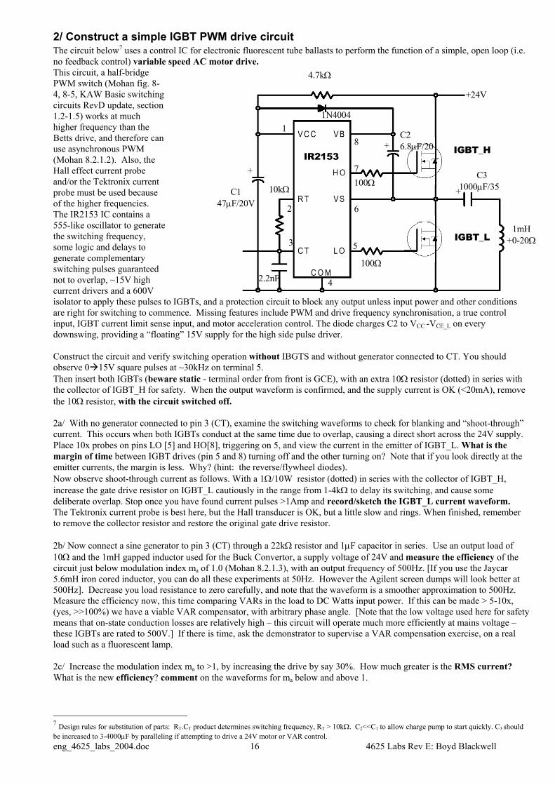
2/ Construct a simple IGBT PWM drive circuit The circuit below7 uses a control IC for electronic fluorescent tube ballasts to perform the function of a simple, open loop (i.e. no feedback control) variable speed AC motor drive. This circuit, a half-bridge PWM switch (Mohan fig. 8-4, 8-5, KAW Basic switching circuits RevD update, section 1.2-1.5) works at much higher frequency than the Betts drive, and therefore can use asynchronous PWM (Mohan 8.2.1.2). Also, the Hall effect current probe and/or the Tektronix current probe must be used because of the higher frequencies. The IR2153 IC contains a 555-like oscillator to generate the switching frequency, some logic and delays to generate complementary switching pulses guaranteed not to overlap, ~15V high current drivers and a 600V isolator to apply these pulses to IGBTs, and a protection circuit to block any output unless input power and other conditions are right for switching to commence. Missing features include PWM and drive frequency synchronisation, a true control input, IGBT current limit sense input, and motor acceleration control. The diode charges C2 to VCC -VCE_L on every downswing, providing a “floating” 15V supply for the high side pulse driver. Construct the circuit and verify switching operation without IBGTS and without generator connected to CT. You should observe 0 15V square pulses at ~30kHz on terminal 5. Then insert both IGBTs (beware static - terminal order from front is GCE), with an extra 10Ω resistor (dotted) in series with the collector of IGBT_H for safety. When the output waveform is confirmed, and the supply current is OK (<20mA), remove the 10Ω resistor, with the circuit switched off. 2a/ With no generator connected to pin 3 (CT), examine the switching waveforms to check for blanking and “shoot-through” current. This occurs when both IGBTs conduct at the same time due to overlap, causing a direct short across the 24V supply. Place 10x probes on pins LO [5] and HO[8], triggering on 5, and view the current in the emitter of IGBT_L. What is the margin of time between IGBT drives (pin 5 and 8) turning off and the other turning on? Note that if you look directly at the emitter currents, the margin is less. Why? (hint: the reverse/flywheel diodes). Now observe shoot-through current as follows. With a 1Ω/10W resistor (dotted) in series with the collector of IGBT_H, increase the gate drive resistor on IGBT_L cautiously in the range from 1-4kΩ to delay its switching, and cause some deliberate overlap. Stop once you have found current pulses >1Amp and record/sketch the IGBT_L current waveform. The Tektronix current probe is best here, but the Hall transducer is OK, but a little slow and rings. When finished, remember to remove the collector resistor and restore the original gate drive resistor. 2b/ Now connect a sine generator to pin 3 (CT) through a 22kΩ resistor and 1µF capacitor in series. Use an output load of 10Ω and the 1mH gapped inductor used for the Buck Convertor, a supply voltage of 24V and measure the efficiency of the circuit just below modulation index ma of 1.0 (Mohan 8.2.1.3), with an output frequency of 500Hz. [If you use the Jaycar 5.6mH iron cored inductor, you can do all these experiments at 50Hz. However the Agilent screen dumps will look better at 500Hz]. Decrease you load resistance to zero carefully, and note that the waveform is a smoother approximation to 500Hz. Measure the efficiency now, this time comparing VARs in the load to DC Watts input power. If this can be made > 5-10x, (yes, >>100%) we have a viable VAR compensator, with arbitrary phase angle. [Note that the low voltage used here for safety means that on-state conduction losses are relatively high – this circuit will operate much more efficiently at mains voltage – these IGBTs are rated to 500V.] If there is time, ask the demonstrator to supervise a VAR compensation exercise, on a real load such as a fluorescent lamp. 2c/ Increase the modulation index ma to >1, by increasing the drive by say 30%. How much greater is the RMS current? What is the new efficiency? comment on the waveforms for ma below and above 1.
7 Design rules for substitution of parts: RT.CT product determines switching frequency, RT > 10kΩ. C2<<C1 to allow charge pump to start quickly. C3 should be increased to 3-4000µF by paralleling if attempting to drive a 24V motor or VAR control.
+24V
4.7kΩ
10kΩ
100Ω
100Ω
1N4004
C26.8µF/20
C147µF/20V
2.2nF
C31000µF/35
1mH+0-20Ω
IR2153IGBT_H
IGBT_L
1
4
2
3
6
8
7
5
+
+
+

eng_4625_labs_2004.doc 17 4625 Labs Rev E: Boyd Blackwell
2d/ If the input is driven too hard, the circuit will perform a fast, orderly shutdown. Try to capture this on the oscilloscope. The criterion used in this chip is that VCT < 1/6 VCC. 3/ Power Dissipation Measurement by Thermal Substitution For FETs, the On-state losses are very low, so the switching loss often dominates. We can estimate on state conduction loss if the voltage and current are almost constant, but the switching voltages and currents change very quickly in time. It is difficult to measure this power; we need simultaneous measurements of V and I over the switch time, and a means of calculating the product (VI) and integrating or averaging it. A much simpler and more fundamental approach is to measure the temperature of the device, apply a DC current so that the temperature is the same, then calculate the DC power from DVM measurements of V and I. The temperature can be measured with better than 1°C resolution with the LM335 device. With a current of around 2mA, the device produces 10mV/K as a Zener, so 300K should be 3.0V. A good plan is to inject a variable bias voltage around 2-5V through a ~Megohm bias resistor into the Gate circuit so that it controls the drain current (IDS) when inverter drive is removed. Pin 5 in the IR2153 circuit would be a good place. Then remove drive for a few seconds at a time, and adjust the bias voltage until the temperature change is minimal. Finally, measure the voltage drop and the FET current in this DC bias condition and calculate power.
eng_4625_labs_2004.doc 18 4625 Labs Rev E: Boyd Blackwell
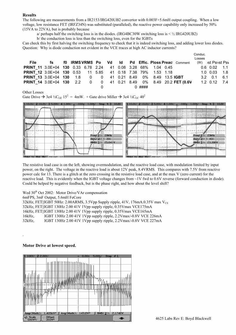
Results The following are measurements from a IR2153/IRG420UB2 convertor with 0.003F+5.6mH output coupling. When a low voltage, low resistance FET (IRFZ34N) was substituted (paralleled), the reactive power capability only increased by 50% (15VA to 22VA), but is probably because
a/ perhaps half the switching loss is in the diodes. (IRG4BC30W switching loss is < ½ IRG420UB2) b/ the conduction loss is less than the switching loss, even for the IGBTs
Can check this by first halving the switching frequency to check that it is indeed switching loss, and adding lower loss diodes. Question: Why is diode conduction not evident in the VCE traces at high AC inductor currents?
File fs f0 IRMS VRMS Po Vd Id Pd Effic. Ploss Preact Comment
Conduc. Losses
(W) est Pswest PswPRINT_11 3.0E+04 130 0.33 6.78 2.24 41 0.08 3.28 68% 1.04 0.45 0.6 0.02 1.1PRINT_12 3.0E+04 130 0.53 11 5.85 41 0.18 7.38 79% 1.53 1.18 1.0 0.03 1.8PRINT_13 3.0E+04 130 1.8 0 0 41 0.21 8.49 0% 8.49 13.5 IGBT 3.2 0.1 6.1PRINT_14 3.0E+04 130 2.2 0 0 41 0.21 8.49 0% 8.49 20.2 FET (0.6V 1.2 0.12 7.4
0 0 ####Other Losses Gate Drive 3e4 ½CGE 152 = 4mW. + Gate drive Miller 3e4 ½CGC 402
The resistive load case is on the left, showing overmodulation, and the reactive load case, with modulation limited by input power, on the right. The voltage in the reactive load is about 12V peak, 8.4VRMS. This compares with 7.5V from reactive power calc for 13. There is a glitch at the zero crossing in the resistive load case, and at the max V (zero current) for the reactive load. This is evidently when the IGBT voltage changes from ~1V fwd to 0.6V reverse (forward conduction in diode). Could be helped by negative feedback, but is the phase right, and how about the level shift? Wed 30th Oct 2002: Motor Drive/VAr compensation 6mFPS, 3mF Output, 5.6mH FeCore 32kHz, FET||IGBT 50Hz: 2.00ARMS, 3.5Vpp Supply ripple, 41V, 176mA.0.35V max VCE 32kHz, FET||IGBT 130Hz 2.00 41V 1Vpp supply ripple, 0.35Vmax VCE175mA 16kHz, FET||IGBT 130Hz 2.00 41V 1Vpp supply ripple, 0.35Vmax VCE165mA 16kHz, IGBT 130Hz 2.00 41V 1Vpp supply ripple, 2.2Vmax/-0.8V VCE 226mA 32kHz, IGBT 130Hz 2.00 41V 1Vpp supply ripple, 2.2Vmax/-0.8V VCE 227mA . Motor Drive at lowest speed.
eng_4625_labs_2004.doc 19 4625 Labs Rev E: Boyd Blackwell
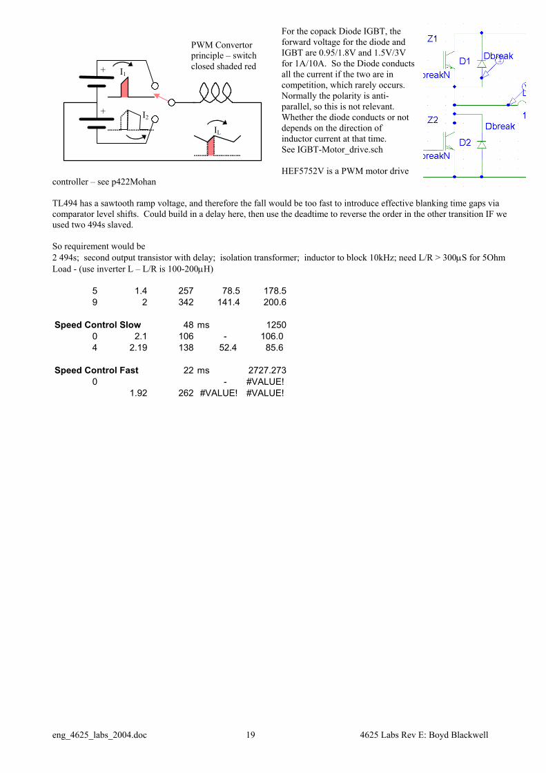
For the copack Diode IGBT, the forward voltage for the diode and IGBT are 0.95/1.8V and 1.5V/3V for 1A/10A. So the Diode conducts all the current if the two are in competition, which rarely occurs. Normally the polarity is anti-parallel, so this is not relevant. Whether the diode conducts or not depends on the direction of inductor current at that time. See IGBT-Motor_drive.sch HEF5752V is a PWM motor drive
controller – see p422Mohan TL494 has a sawtooth ramp voltage, and therefore the fall would be too fast to introduce effective blanking time gaps via comparator level shifts. Could build in a delay here, then use the deadtime to reverse the order in the other transition IF we used two 494s slaved. So requirement would be 2 494s; second output transistor with delay; isolation transformer; inductor to block 10kHz; need L/R > 300µS for 5Ohm Load - (use inverter L – L/R is 100-200µH)
5 1.4 257 78.5 178.59 2 342 141.4 200.6
Speed Control Slow 48 ms 12500 2.1 106 - 106.0 4 2.19 138 52.4 85.6
Speed Control Fast 22 ms 2727.273
0 - #VALUE! 1.92 262 #VALUE! #VALUE!
+
+ I2
I1
PWM Convertor principle – switch closed shaded red
IL

eng_4625_labs_2004.doc 20 4625 Labs Rev E: Boyd Blackwell
Laboratory Reports Two reports are to be written up “formally”. The rest are either lab. notebook style, or sheets to be filled in. Formal reports Length: Maximum 7 pages 12pt type. If Graphs and figures are attached separately, they count as 1/3 page each graph/figure. Figures: No requirement or extra marks for computer drawn graphs/figures, but in either form, they must be reasonably neat. Content: Abstract, introduction and conclusion should be brief and to the point. Good presentation, analysis and discussion of results is more important. Numbering: Use the lab handout numbering to make it clear which part you are answering, Most frequent loss of marks is omission of a part of the work. I recommend that you show me your report when it is close to completion, to check for glaring errors.
Comments on Reports Most frequent loss of marks 1/ not doing a part that is required 2/ Results wacky (not just a little bit out) 3/ too much effort on introduction, abstract, conclusion at the expense of statement and discussion of results. Abstracts etc are OK, but are not required, and were sometimes too long. Rule of thumb – if you feel that what you are saying is so general that it really doesn’t say much at all, then don’t say it. Stick with my numbering scheme (e.g. part2a is FW) please, or at least refer to it, to make marking easier No penalty for grouping all together into intro/method/results/conclusion, but certainly lab 1 was better done one subject at a time, and you didn’t need all of these sections for many of the parts. Most frequent mistakes in Lab 1 no equation for vripple or vload no discussion of effect of transformer Z 1d/ no RMS estimation, or used Ipeak/√2] No spectrum 2/a I did not think of this at the time (so no penalty), but IRMS for the transformer must be √2 × IRMS (diode, AC+DC), as the transformer current is “two copies: of one diode current pulse. Think of the definition of RMS as to how it is √2 – nothing to do with peak to RMS ratio this time!. Also, those of you who took the diode current pulse to be a half cycle of 100Hz, the RMS, by the same logic, is 1/√4 = ½ that of a full 50Hz cycle, not ¼. Why did I say AC+DC RMS of the diode above? (yes, the DC component is zero in the Itrans, but) RMS formally includes both AC and DC! Try it in pSpice if you don’t believe me. RMS is best done 3. Power in load needs to include resistance of inductor. 4 Wrong Spectrum (asked for I (Vsource) not load or diode) – but no penalty as I can see my notes are ambiguous 5 No power analysis, Transformer power = 7W – wrong – way too high – maybe this was the power from the DC supply. General Power dissipation in resistor (not power across resistor) Voltage across is fine Power out of transformer ~20W, power loss in transformer ~0.5W. Many people had > ½ page discussion for each section, most did not help much. 3 or 4 were very good, and got extra marks, but even so , 1 of those lost the marks again later on something he did not have time to complete. To do In your discussion of Quiz solutions DC Motor vs AC Motor Exam: 2½ Hours, 5 of 7 short answers, 3 or 5 other questions, one double-side a4 page like the sample exam. The laboratory related component of the exam is around 25% of the total mark, but there is no point in trying to putting any your results on the a4 sheet – an understanding of the work is what is important.
Hints for Fuses and Power Quality Labs I have mentioned these to all groups in the lab, but I put them up on the web in case any of these were missed. Fuses Lab: • A simpler way to present the results is to put them all (all fuses and circuit breaker) on one log-log graph, similar to the
graph given, with t on the y axis and I/Inominal on the x axis. (I nominal for the circuit breaker is 2Amps, most fuses 0.5A, except some were 1A, including the fast ceramic.
Itrans Idiode

eng_4625_labs_2004.doc 21 4625 Labs Rev E: Boyd Blackwell
• If done this way, you don’t have to plot I2t: you can instead draw a straight line of slope –2; this will be a graph of constant I2t.
• The time to zero I refer to is the time from the beginning of the pulse to the current zero, and is typically the same as time to rupture.
Power Quality • This lab is the work of two people. You must acknowledge data “borrowed” from others, briefly explaining why. • Make it clear which load you describe. • The third row of the current and voltage table was labelled Relative voltage or current – it should have read
RMS voltage(V) and RMS Current(A) respectively. The fourth column is still relative - Power rel. to fund. • Replace “normal” and “other” with the specific conditions for your load • Question 2: The two forms for PF given should both be evaluated, tabulated and the values compared. They are two ways
of measuring the same thing, the general PF. The first is straight out of Mohan, but relies on a phase angle of a non-sinusoid. The second is an explicit evaluation of power used relative to the equivalent power the distribution systems could have delivered into an ideal, linear resistive load for the same heating effect on transformers, transmission lines and other distribution components. It requires a digital CRO or similar to evaluate, but does not assume anything about phase. I used the notation of Mohan p42 in the first expression, so IS ≡ IRMS and IS1 = RMS value of fundamental current. (references to “converting fundamental amplitude to RMS” are irrelevant this year, as the CRO’s both refer their dB values to unity RMS values directly 1ARMS, 1VRMS).
• Question 5b - The table of harmonic current distortion maximum values I was referring to in Mohan is on p486 – use the top line. (Isc/I1 < 20)
• You should be able to deduce the equivalent series inductance and resistance (of the induction motor and the uncompensated fluorescent light – not the drill) from V/I = Z = R + jωL.