Embed Size (px)
Citation preview

ENGLINKS.CA
Academic Support Service of the
Engineering Society of Queen’s
University
ELEC 271 Review Created by Madeline Van Der Paelt

i
Hi there! Just some thoughts to get you started…
I created this review package to help ECE students understand ELEC 271, but I am not perfect. So please
use this as a reference to freshen up on material, but study from more than just this! These are just
some summarized notes and brief explanations. For more depth and detail, consult a TA or the
professor. All of the solutions and examples are correct to the best of my knowledge, but they may not
be perfect. My biggest tips are to ask your lab TA’s for help, study from old finals and actually do your
labs. If you understand the labs, you’re golden.
Good luck!
Ps. The textbook actually has some good examples and diagrams too.
Madeline Van Der Paelt. Sci 17
Contents Hi there! ......................................................................................................................................................... i
A Quick VHDL Tutorial… ................................................................................................................................ 1
Boolean Algebra ............................................................................................................................................ 1
Things to know .......................................................................................................................................... 1
Boolean Algebra Properties ...................................................................................................................... 1
Sum of Products (SOP) .............................................................................................................................. 1
Product of Sums (POS) .............................................................................................................................. 1
Minterms and Maxterms .......................................................................................................................... 2
Karnaugh Maps ......................................................................................................................................... 2
Implicants .............................................................................................................................................. 2
How to use it: ........................................................................................................................................ 3
Drawing Logic Networks ........................................................................................................................... 4
De Morgan’s Theorem .............................................................................................................................. 4
Transistors, NAND and NOR .......................................................................................................................... 4
Things to know .......................................................................................................................................... 4
Transistors: ................................................................................................................................................ 5
Optimization ................................................................................................................................................. 5
Things to know .......................................................................................................................................... 5
FPGA’s ........................................................................................................................................................... 6

ii
Things to know .......................................................................................................................................... 6
Look-Up Tables .......................................................................................................................................... 6
Drawing a 2-input LUT .............................................................................................................................. 6
Boolean Algebra ........................................................................................................................................ 7
Combinational Circuits .................................................................................................................................. 7
Things to know .......................................................................................................................................... 7
Multiplexers .............................................................................................................................................. 7
Encoders/Decoders ................................................................................................................................... 8
Number Representation and Arithmetic ...................................................................................................... 8
Things to know .......................................................................................................................................... 8
Binary ........................................................................................................................................................ 8
Adders ....................................................................................................................................................... 9
Latches and Flip-Flops ................................................................................................................................. 10
Things to know ........................................................................................................................................ 10
Latches .................................................................................................................................................... 10
NOR Based SR Latch ................................................................................................................................ 10
NAND Only SR Latch ................................................................................................................................ 10
Gated D Latch .......................................................................................................................................... 11
Clear, Preset and Load Enable ................................................................................................................ 11
Timing Diagrams ..................................................................................................................................... 11
VHDL Implementation............................................................................................................................. 13
Sequential Circuits and State Machines...................................................................................................... 14
Things to know ........................................................................................................................................ 14
Design Steps ............................................................................................................................................ 14
State Diagram.......................................................................................................................................... 14
State Table .............................................................................................................................................. 15
Minimization of States (Partitioning) ...................................................................................................... 16
Moore and Mealy.................................................................................................................................... 17
Next State Logic ...................................................................................................................................... 17
Output Logic ............................................................................................................................................ 17
VHDL Implementation............................................................................................................................. 18
References .................................................................................................................................................. 19
1
A Quick VHDL Tutorial… At a minimum an entity and an architecture usually need to be defined. Think of the entity like an object
of sorts. Within the entity you must define the port mapping – basically what are the inputs/outputs and
their types. “Std_logic” is used as the type in the examples below, however you may also use things like
“std_logic_vector(3 downto 0)” in labs. When you are referencing or assigning a signal that is of type
“std_logic”, the value should be surrounded by single quotes (ex. q <= ‘0’). When referencing or
assigning a signal that is a “std_logic_vector” the value should be surrounded by double quotes. The
architecture is like the “main” with other processes defined within it. You must always have a being and
end statement.
Boolean Algebra
Things to know Boolean algebra properties
Sum of products VS Product of Sums
How to generate and use a Karnaugh Map
How to draw logic networks
De Morgan’s Theorem (and other operations)
Boolean Algebra Properties Refer to the formula sheet that the professor most likely made you fill out in class. There are too many
to go through them all in detail here. Know how to use the formulas to simplify or expand a given
equation. The key to manipulating these problems is practice. Do them over and over until you are
comfortable with them. The rules of Boolean algebra are explained really well on Electronics-Tutorials
[1]. A link to the webpage is available with the reference at the end of this document.
Sum of Products (SOP) Minterms are combined with an “or” operation (+)
Equation will use the symbol Σ
Represented with “1” in a Karnaugh Map
0’s complemented when creating simplified equation
Tip: Sum of products – think addition, which uses the same symbol
Ex. f(x, y, z) = Σ(m0, m2, m3)
Product of Sums (POS) Maxterms are combined with an “and” operation (●)
Equation will use the symbol Π
Represented with “0” in a Karnaugh Map
1’s complemented when creating simplified equation
Tip: Product of sums – think multiplication, which uses the same symbol
Ex. f(x, y, z) = Π(m1, m4, m5, m6, m7)

2
Minterms and Maxterms 1. Make a truth table for the number of variables. Ex. 3 variable truth table in Table 1.
2. Identify minterms
3. If it isn’t a minterm then it has to be a maxterm!
Table 1: Three variable truth table (inputs only)
Term x y z
0 0 0 0
1 0 0 1
2 0 1 0
3 0 1 1
4 1 0 0
5 1 0 1
6 1 1 0
7 1 1 1
Karnaugh Maps Very useful to simplify logic networks!
Usually 3 or 4 variables.
o 3 – use 2 rows, 4 columns
o 4 – use 4 rows, 4 columns
o 5 – use two 4 variable tables side by side. Left uses fifth variable = 0, right = 1. See your
professor’s notes for more if this comes up for a lab.
The map should be set up as follows for a 4 variable problem. Note the order of the labels
(black) and the min/max terms (purple).
00 01 11 10
00 0 1 3 2
01 4 5 7 6
11 12 13 15 14
10 8 9 11 10
Implicants
Implicant = product terms for one or more valuations where the output is 1
Prime Implicant = an implicant that cannot be combined with any other implicant
Least-cost expression = a subset of prime implicants
Don’t cares = can be a 1 or a 0, whichever is preferable, allowing you to make larger groupings
and further simplify the expression
In other words…
Let’s say you’re doing a SOP (swap 1 for 0 in a POS). When you group the 1’s in the Karnaugh map, each
grouping is called an implicant. Then each grouping that contains a unique element (a 1 not covered by
another group) is a prime implicant – the only way to include that value. The least cost expression, is
made up of the smallest set of prime implicants that covers all values.

3
wx yz wx yz
How to use it: 1. Draw the grid as described above.
2. Fill minterms with 1’s or maxterms with 0’s and any don’t cares with d’s
3. Circle the largest power of 2 groups. (Groups of 2, 4, 8, 16…) Note the four corners can be
grouped or the outside edges!
4. Look at a grouping, see which variable(s) change and which stay the same. Create terms
a. For POS: create a sum term using the unchanging variables. Complement the 1’s.
b. For SOP: create a product term using the unchanging variables. Complement the 0’s.
5. Create the equation
a. For POS: join terms with an “and”
b. For SOP: join terms with an “or”
Ex. Sum of Products for 𝑓(𝑤, 𝑥, 𝑦, 𝑧) = ∑(𝑚1, 𝑚2, 𝑚5, 𝑚7, 𝑚10, 𝑚15)
a) Fill in minterms b) circle groups
With help placing the minterms, refer to the sample mapping above.
There are 4 implicants or groupings, however only 3 of them are prime. The orange group contains a 1
at 0001, which is not covered by another group and is therefore prime. The blue group contains a 1 at
1111 which is not covered by another group, and so it is prime. Both 1’s in the purple group are uniquely
covered by that group so it too is prime. The red group contains only 1’s covered by the blue and orange
groups, and nothing unique, so it is not prime.
Looking at the placement of the 1’s in the orange group, the column does not change (y and z are
unchanging) and between the rows, w remains a 0 while x changes. The unchanging variables are w=0,
y=0 and z=1. It is a SOP so we make product terms and sum them and we invert the 0’s. The product
term for this group is �̅� ∙ �̅� ∙ 𝑧 or �̅��̅�𝑧.
In the blue group y=1, z=1 and x=1 are unchanging, so we get 𝑥𝑧𝑦. In the purple group, x=0, y= 1, and
z=0 are unchanging, which makes �̅�𝑦𝑧̅
For the final equation, make a sum of the product terms… 𝑓(𝑤, 𝑥, 𝑦, 𝑧) = �̅��̅�𝑧 + 𝑥𝑧𝑦 + �̅�𝑦𝑧̅
00 01 11 10
00 1 1
01 1 1
11 1
10 1
00 01 11 10
00 1 1
01 1 1
11 1
10 1

4
Drawing Logic Networks Canonical = original, un-simplified equation. (Usually larger and uglier than the simplified
network)
Know the symbols…
Figure 1: Standard logic gates [2]
De Morgan’s Theorem Key: Swap the connecting sign and invert the variables
Examples:
𝑎 ∙ 𝑏̅̅ ̅̅ ̅̅ = �̅� + �̅�
𝑎 + 𝑏̅̅ ̅̅ ̅̅ ̅ = 𝑎 ̅ ∙ �̅�
�̅� + 𝑏̅̅ ̅̅ ̅̅ ̅ = 𝑎�̅�
𝑎𝑏 + 𝑐𝑑̅̅ ̅̅ ̅̅ ̅̅ ̅̅ = 𝑎𝑏̅̅ ̅ ∙ 𝑐𝑑̅̅ ̅ This can use De Morgan’s again! 𝑎𝑏̅̅ ̅ ∙ 𝑐𝑑̅̅ ̅ = (�̅� + �̅�) ∙ (𝑐̅ + �̅�)
Transistors, NAND and NOR
Things to know NAND and NOR Gates effectively invert the output of an “and” or “or” operation respectively
NMOS, PMOS and CMOS transistors
o How to generate each
o How they work together

5
Transistors: 1. Draw NMOS
a. “or” = parallel (this path or the other)
b. “and” = series (you have to go through both)
2. Draw PMOS - opposite
a. “or” = series
b. “and” = parallel
c. Note: uses the inverter (---o|) See sample question for clarification.
3. Draw CMOS
a. Place the PMOS on top and the NMOS underneath.
4. Fill in the chart if required.
a. NMOS – low = off, high = on
b. PMOS – low = on, high = off.
c. Output – trace the “on” transistors. If the path goes “dead” before hitting VDD and is
alive leading to ground then it is low. If the live path goes to VDD it is high.
TIP: NMOS is the most natural (intuitive) so remember it, and know that PMOS is the exact opposite.
Ex. 𝑓(𝑥, 𝑦, 𝑧) = 𝑥(𝑦 + 𝑧)̅̅ ̅̅ ̅̅ ̅̅ ̅̅ ̅
Optimization
Things to know Optimization = Karnaugh maps, go back to question 1.

6
FPGA’s
Things to know Look-Up Tables
Boolean Algebra
Look-Up Tables Contain storage cells for 1 or 0 outputs, corresponding to the outputs of a truth table.
To figure out how many LUT’s are needed to directly implement a function, the easiest way is to
make groups of inputs and operations.
Ex. How many LUT’s are needed to directly implement 𝑓(𝑎, 𝑏, 𝑐, 𝑑) = �̅�𝑏 + 𝑏𝑐𝑑 + 𝑎𝑑 using 2-
input look up tables?
�̅�𝑏 = �̅� ∙ 𝑏 The “and” of two inputs would need 1 LUT
𝑎𝑑 = 𝑎 ∙ 𝑑 Again, 1 LUT to “and” two inputs
𝑏𝑐𝑑 = 𝑏 ∙ 𝑐 ∙ 𝑑 = (𝑏 ∙ 𝑐) ∙ 𝑑 1 LUT to for b “and” c, and 1 LUT to “and” the output with d
We need 2 more LUT’s to cover the two “or” operations
TOTAL: 6 LUT’s
TIP: I find it easiest to write out the equation, and draw the groupings as follows…
Drawing a 2-input LUT 1. Draw 2 input truth table
2. Draw 1 column with 4 rows next to the truth table and evaluate the expression given
3. Draw 2 flip-flops next to the truth table, and a third connecting the first two.
4. Draw the appropriate connections
Ex.1 Draw the direct implementation of the first product term for 𝑓(𝑎, 𝑏, 𝑐, 𝑑) = �̅�𝑏 + 𝑏𝑐𝑑 + 𝑎𝑑.
Note: The highlighted terms are those used to evaluate the
equation and produce the outputs in the boxes.
�̅� 𝑎 𝑏
1 0 0 1 0 1 0 1 0 0 1 1
0 1
0 1
0 1
�̅�𝑏
0 1 0 0
1 2 3 4
5 6
𝑓(𝑎, 𝑏, 𝑐, 𝑑) = �̅�𝑏 + 𝑏𝑐𝑑 + 𝑎𝑑
Steps: 1 2 3&4
7
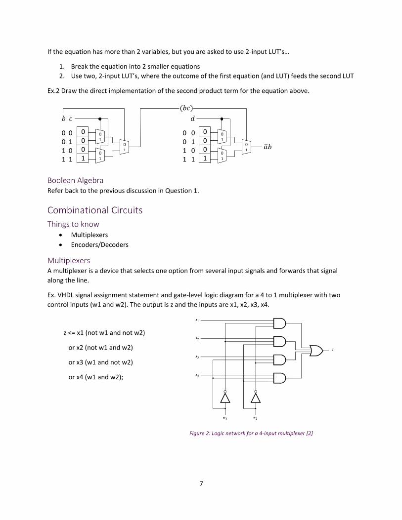
If the equation has more than 2 variables, but you are asked to use 2-input LUT’s…
1. Break the equation into 2 smaller equations
2. Use two, 2-input LUT’s, where the outcome of the first equation (and LUT) feeds the second LUT
Ex.2 Draw the direct implementation of the second product term for the equation above.
Boolean Algebra Refer back to the previous discussion in Question 1.
Combinational Circuits
Things to know Multiplexers
Encoders/Decoders
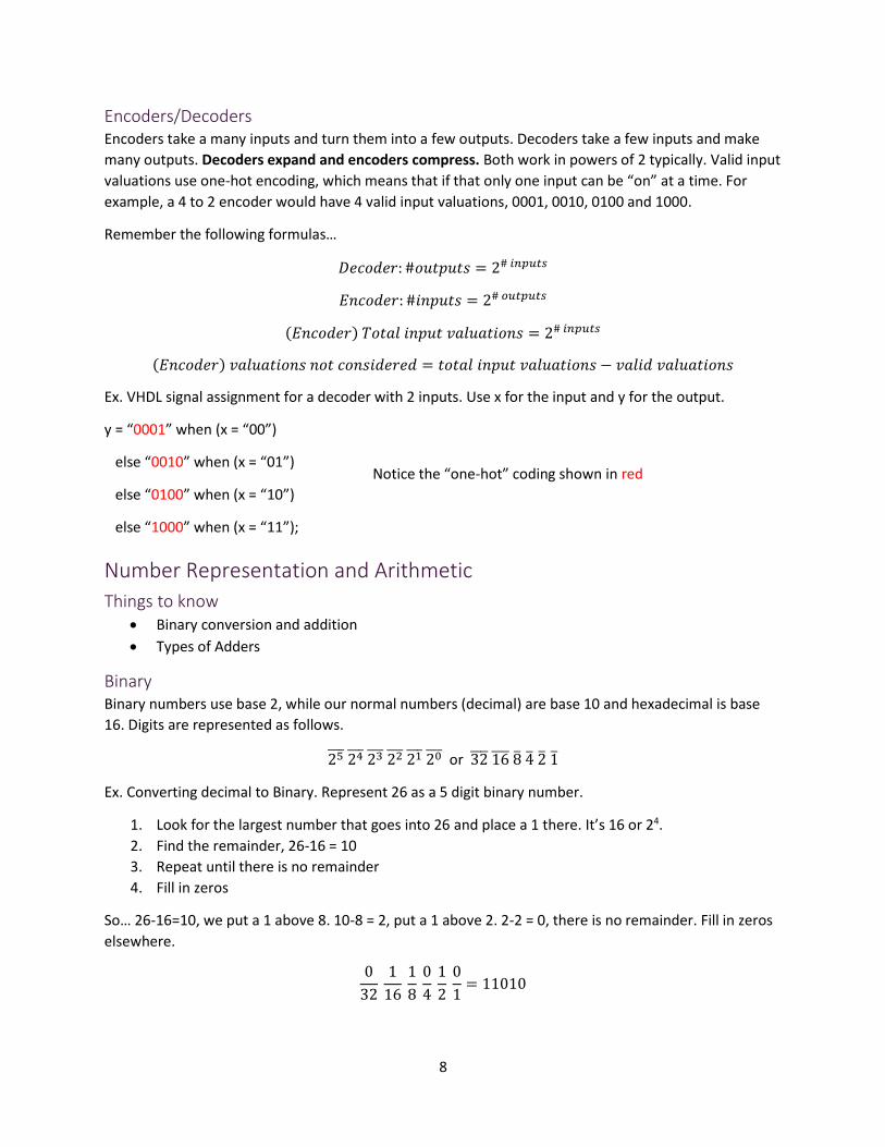
Multiplexers A multiplexer is a device that selects one option from several input signals and forwards that signal
along the line.
Ex. VHDL signal assignment statement and gate-level logic diagram for a 4 to 1 multiplexer with two
control inputs (w1 and w2). The output is z and the inputs are x1, x2, x3, x4.
Figure 2: Logic network for a 4-input multiplexer [2]
𝑏 𝑐
0 0 0 1 1 0 1 1
0 1
0 1
0 1
0 0 0 1
𝑑
0 0 0 1 1 0 1 1
0 1
0 1
0 1
�̅�𝑏
(𝑏𝑐)
0 0 0 1
z <= x1 (not w1 and not w2)
or x2 (not w1 and w2)
or x3 (w1 and not w2)
or x4 (w1 and w2);
8
Encoders/Decoders Encoders take a many inputs and turn them into a few outputs. Decoders take a few inputs and make
many outputs. Decoders expand and encoders compress. Both work in powers of 2 typically. Valid input
valuations use one-hot encoding, which means that if that only one input can be “on” at a time. For
example, a 4 to 2 encoder would have 4 valid input valuations, 0001, 0010, 0100 and 1000.
Remember the following formulas…
𝐷𝑒𝑐𝑜𝑑𝑒𝑟: #𝑜𝑢𝑡𝑝𝑢𝑡𝑠 = 2# 𝑖𝑛𝑝𝑢𝑡𝑠
𝐸𝑛𝑐𝑜𝑑𝑒𝑟: #𝑖𝑛𝑝𝑢𝑡𝑠 = 2# 𝑜𝑢𝑡𝑝𝑢𝑡𝑠
(𝐸𝑛𝑐𝑜𝑑𝑒𝑟) 𝑇𝑜𝑡𝑎𝑙 𝑖𝑛𝑝𝑢𝑡 𝑣𝑎𝑙𝑢𝑎𝑡𝑖𝑜𝑛𝑠 = 2# 𝑖𝑛𝑝𝑢𝑡𝑠
(𝐸𝑛𝑐𝑜𝑑𝑒𝑟) 𝑣𝑎𝑙𝑢𝑎𝑡𝑖𝑜𝑛𝑠 𝑛𝑜𝑡 𝑐𝑜𝑛𝑠𝑖𝑑𝑒𝑟𝑒𝑑 = 𝑡𝑜𝑡𝑎𝑙 𝑖𝑛𝑝𝑢𝑡 𝑣𝑎𝑙𝑢𝑎𝑡𝑖𝑜𝑛𝑠 − 𝑣𝑎𝑙𝑖𝑑 𝑣𝑎𝑙𝑢𝑎𝑡𝑖𝑜𝑛𝑠
Ex. VHDL signal assignment for a decoder with 2 inputs. Use x for the input and y for the output.
y = “0001” when (x = “00”)
else “0010” when (x = “01”)
else “0100” when (x = “10”)
else “1000” when (x = “11”);
Number Representation and Arithmetic
Things to know Binary conversion and addition
Types of Adders
Binary Binary numbers use base 2, while our normal numbers (decimal) are base 10 and hexadecimal is base
16. Digits are represented as follows.
25̅̅ ̅ 24̅̅ ̅ 23̅̅ ̅ 22̅̅ ̅ 21̅̅ ̅ 20̅̅ ̅ or 32̅̅̅̅ 16̅̅̅̅ 8̅ 4̅ 2̅ 1̅
Ex. Converting decimal to Binary. Represent 26 as a 5 digit binary number.
1. Look for the largest number that goes into 26 and place a 1 there. It’s 16 or 24.
2. Find the remainder, 26-16 = 10
3. Repeat until there is no remainder
4. Fill in zeros
So… 26-16=10, we put a 1 above 8. 10-8 = 2, put a 1 above 2. 2-2 = 0, there is no remainder. Fill in zeros
elsewhere.
0
32
1
16 1
8 0
4 1
2 0
1= 11010
Notice the “one-hot” coding shown in red

9
Ex. Binary addition. Add 12 and 26 in binary.
From the previous example, 26 = 11010 in binary. Using the same method, 12 is represented as 01100.
1. Set up the equation
11010+01100
?
2. Perform addition. 0+0 = 00 (no carry), 0+1 = 01 (no carry), 1+1 = 10 (or 2, carry the 1)
11010+01100 ? ? ? ? 0
11010+01100 ? ? ?10
11010+01100 ? ?110
1 11010+01100 ?0110
11010+01100 100110
3. Convert result from binary to decimal to check answer
100110 = 32+4+2 = 38
12+26 = 38
Adders Half Adder - has 2 single bit inputs (the numbers being added) and 2 outputs (sum and carry)
Full Adder – 3 single bit inputs (the 2 numbers being added and a carry in), and 2 outputs (sum
and carry out)
Ripple-Carry Adder – a collection of full adders used to add 2 multi-bit numbers. Each output
carry becomes the input carry for the next adder.
Fast Adder or Carry-Lookahead Adder– similar to a ripple carry in that it is for 2 multi-bit
numbers and uses multiple full adders. However, it splits up the operations into 2 functions to
speed up the operation.
o Propagate: propagates the carry from the previous stage. 𝑝𝑖 = 𝑥𝑖 + 𝑦𝑖
o Generate: generates the carry for the current stage. 𝑔𝑖 = 𝑥𝑖𝑦𝑖
o 𝑐𝑖+1 = 𝑥𝑖𝑦𝑖 + (𝑥𝑖 + 𝑦𝑖)𝑐𝑖 = 𝑔𝑖 + 𝑝𝑖𝑐𝑖
o 𝑠𝑖 = 𝑐𝑖⨁𝑥𝑖⨁𝑦𝑖
o Logic levels
1. Produce all 𝑝𝑖 and 𝑔𝑖 values
2. Perform “and” of 𝑝𝑖 and 𝑐𝑖−1
3. Produce 𝑐𝑖 values; “or” 𝑔𝑖 and the output of step 2.
4. Produce 𝑠𝑖 values
10
Latches and Flip-Flops
Things to know NOR vs NAND gated SR Latches
Gated D Latch
𝐶𝑙𝑒𝑎𝑟̅̅ ̅̅ ̅̅ ̅̅ , 𝑃𝑟𝑒𝑠𝑒𝑡̅̅ ̅̅ ̅̅ ̅̅ ̅ and 𝐿𝑜𝑎𝑑 𝐸𝑛𝑎𝑏𝑙𝑒
Timing diagrams
VHDL flip-flop implementation
Latches Latches are often controlled using a clock signal (clk). When clk = 0, S’ and R’ = 0, and there can be no
change to the state of the latch. When clk = 1, S’ and R’ follow S and R respectively which determine if
there is a change.
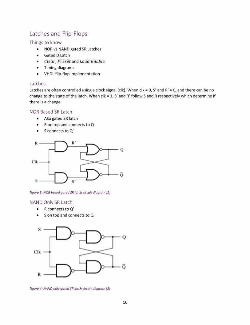
NOR Based SR Latch Aka gated SR latch
R on top and connects to Q
S connects to Q’
Figure 3: NOR based gated SR latch circuit diagram [2]
NAND Only SR Latch R connects to Q’
S on top and connects to Q
Figure 4: NAND only gated SR latch circuit diagram [2]
11
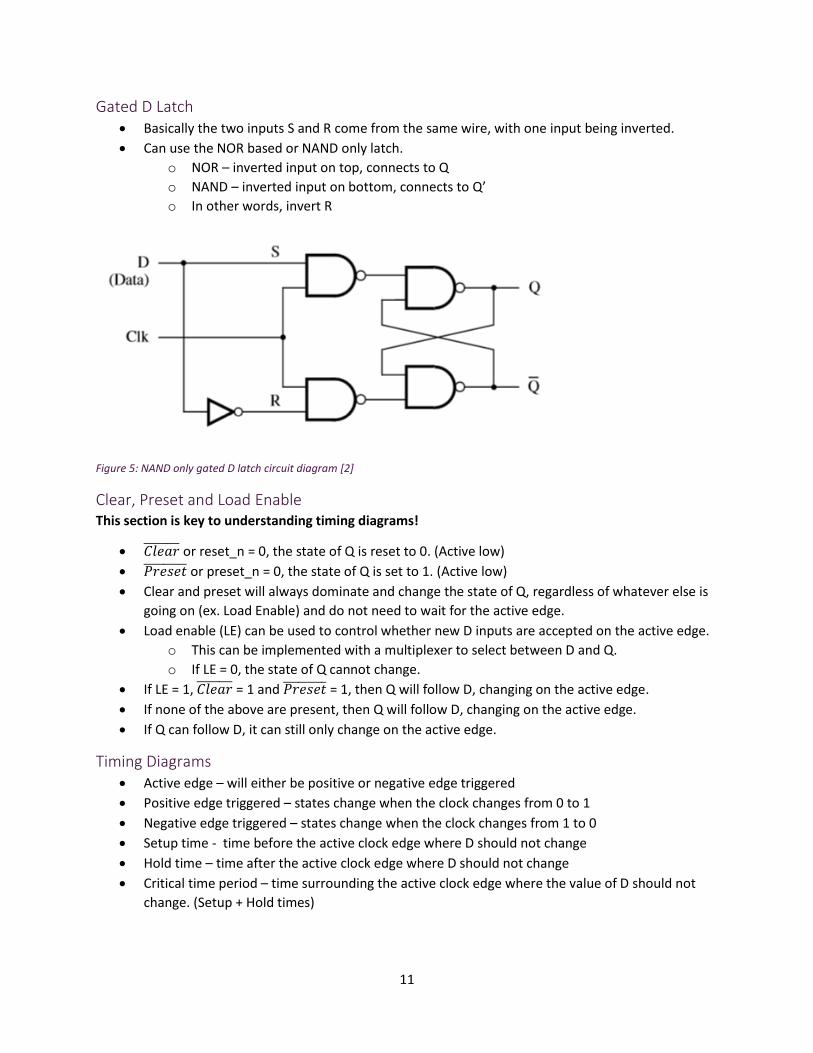
Gated D Latch Basically the two inputs S and R come from the same wire, with one input being inverted.
Can use the NOR based or NAND only latch.
o NOR – inverted input on top, connects to Q
o NAND – inverted input on bottom, connects to Q’
o In other words, invert R
Figure 5: NAND only gated D latch circuit diagram [2]
Clear, Preset and Load Enable This section is key to understanding timing diagrams!
𝐶𝑙𝑒𝑎𝑟̅̅ ̅̅ ̅̅ ̅̅ or reset_n = 0, the state of Q is reset to 0. (Active low)
𝑃𝑟𝑒𝑠𝑒𝑡̅̅ ̅̅ ̅̅ ̅̅ ̅ or preset_n = 0, the state of Q is set to 1. (Active low)
Clear and preset will always dominate and change the state of Q, regardless of whatever else is
going on (ex. Load Enable) and do not need to wait for the active edge.
Load enable (LE) can be used to control whether new D inputs are accepted on the active edge.
o This can be implemented with a multiplexer to select between D and Q.
o If LE = 0, the state of Q cannot change.
If LE = 1, 𝐶𝑙𝑒𝑎𝑟̅̅ ̅̅ ̅̅ ̅̅ = 1 and 𝑃𝑟𝑒𝑠𝑒𝑡̅̅ ̅̅ ̅̅ ̅̅ ̅ = 1, then Q will follow D, changing on the active edge.
If none of the above are present, then Q will follow D, changing on the active edge.
If Q can follow D, it can still only change on the active edge.
Timing Diagrams Active edge – will either be positive or negative edge triggered
Positive edge triggered – states change when the clock changes from 0 to 1
Negative edge triggered – states change when the clock changes from 1 to 0
Setup time - time before the active clock edge where D should not change
Hold time – time after the active clock edge where D should not change
Critical time period – time surrounding the active clock edge where the value of D should not
change. (Setup + Hold times)

12
Ex. Timing diagram for a positive edge triggered D flip flop which has an asynchronous active low reset
and preset, and a load enable input.
Figure 6: Completed timing diagram [3]
(Blue) Preset_n = 0, so Q is 0. Then preset_n = 1 and LE = 0 so Q cannot change and is stuck at 0, then LE
= 1 and preset_n and reset_n = 1, so Q can follow D, but not until the positive edge.
(Orange) Q can follow D, but at the positive edge (where blue meets orange) D = 0 so Q is still 0. D
moves to 1 on, but the change is not detected until the next positive edge (where orange meets purple).
(Purple) Q can follow D (LE = reset_n = preset_n = 1) and D = 1, so Q is now 1. LE is then turned off, so Q
will not follow D on the next edge and is stuck at 1.
(Green) reset_n = 0, which forces Q to 0.
Between the dashed yellow lines is the hold time, and between the dark blue dashed lines is the setup
time. The critical time period contains both the setup and hold times.

13
VHDL Implementation The following code shows examples of gated D flip flop definitions with different capabilities. Reset and
preset are implemented in the same manner, but with different values in the “if statement” and for q.
Note that these are examples of a positive edge triggered flip flop, as they check that clock is 1. A
negative edge triggered flip flop would require that the clock were 0.
entity my_dff is port(d, clk : IN std_logic; q : OUT std_logic); end entity; architecture behaviour of my_dff is begin my_dff : process(clk) begin if (clk’event and clk = ’1’) then q <= d; end if; end process; end architecture;
entity my_dff is port(d, clk, reset_n : IN std_logic; q : OUT std_logic); end entity; architecture behaviour of my_dff is begin my_dff : process(clk, reset_n) begin if (reset_n = ‘0’) then q <= ‘0’; elsif (clk’event and clk = ’1’) then q <= d; end if; end process; end architecture;
entity my_dff is port(d, clk, le : IN std_logic; q : OUT std_logic); end entity; architecture behaviour of my_dff is begin my_dff : process(clk) begin if (clk’event and clk = ’1’) then if (le = ‘1’) then q <= d; end if; end if; end process; end architecture;
a) Basic flip flop b) Flip flop with reset capability c) Flip flop with load enable

14
Sequential Circuits and State Machines
Things to know What are they?
Design steps
Moore Vs. Mealy
Partitioning
State diagram tables
Generating optimized logical expressions
VHDL implementation
In a sequential circuit, the outputs depend on the previous behavior. A state machine uses a sequential
circuit to complete a task; moving through it step by step. Most likely there will be a lab that deals with
this topic, and you will see the effect. An example would be making the lights on the DE0 board light up
one by one and then go out in the reverse order.
Design Steps 1. State Diagram
2. State Table and State Assignment
3. Minimization
4. Select Type – Moore or Mealy
5. Next-State Logic
6. Output Logic
7. Implement Circuit
State Diagram A state diagram is a graphical representation of the states and their transitions. A circular node is used
to represent a state, and an arched arrow to show transitions. To be properly labeled, each node must
contain a unique state label and all outputs generated by the state with their value. Transitions should
be labeled with any conditions required for the transition to occur.
To generate a state diagram
1. Identify the number of states required and the transitions between them
2. Identify the initial/reset state
3. Draw nodes
4. Draw transition connections
5. Label all nodes and transitions appropriately
15
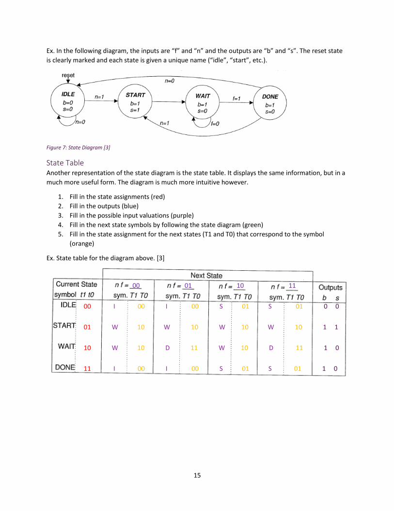
Ex. In the following diagram, the inputs are “f” and “n” and the outputs are “b” and “s”. The reset state
is clearly marked and each state is given a unique name (“idle”, “start”, etc.).
Figure 7: State Diagram [3]
State Table Another representation of the state diagram is the state table. It displays the same information, but in a
much more useful form. The diagram is much more intuitive however.
1. Fill in the state assignments (red)
2. Fill in the outputs (blue)
3. Fill in the possible input valuations (purple)
4. Fill in the next state symbols by following the state diagram (green)
5. Fill in the state assignment for the next states (T1 and T0) that correspond to the symbol
(orange)
Ex. State table for the diagram above. [3]
00 I 00 I 00 S 01 S 01 0 0
01 W 10 W 10 W 10 W 10 1 1
10 W 10 D 11 W 10 D 11 1 0
11 I 00 I 00 S 01 S 01 1 0
00 01 10 11

16
Minimization of States (Partitioning) The idea of partitioning is to see if any of the states are equivalent and therefore redundant. If they are functionally equivalent, then one of them can be taken out of the system, and the state machine can be minimized (More useful with systems larger than those likely to be on the exam) Algorithm: Partition 1: Assume all equivalent Partition 2: Separate based on outputs -if output is the same --> keep in same block -if output is different --> separate into new block Partition 3: Separate based on next state -if next state is the same for all input evaluations --> keep together in block -else --> separate into a new block Partition 4+: Repeat 3 until nothing changes further. Ex. See question 8a) on the ELEC 271 2012 final exam P1: (ISWD) P2: (I)(S)(WD) -W and D both have b=1 and s=0 as their outputs, I and S are unique and are
therefore in their own partitions P3: (I)(S)(W)(D) -D has a next state of I if n=0 or S if n=1, W has a next state of D if f=1 or W if
f=0. These do not match at all and therefore D and W are not equivalent --> separate them.
Tip: If none of the states have the same outputs (within the bubbles), then no work is needed, it cannot be minimized!
17
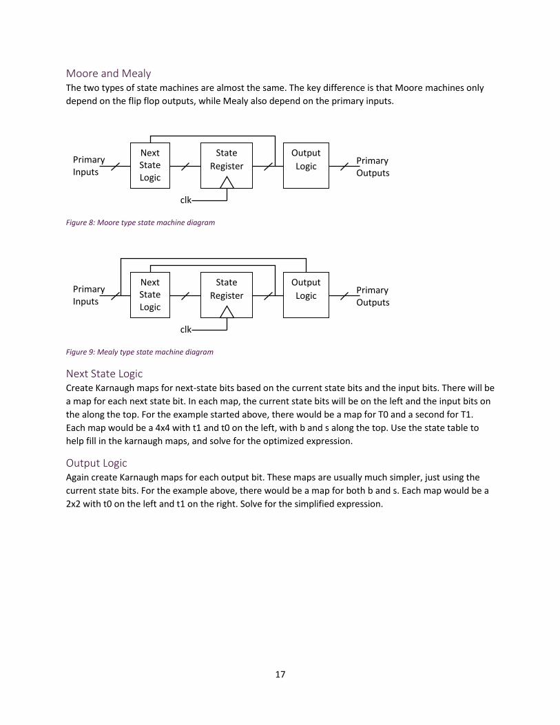
Moore and Mealy The two types of state machines are almost the same. The key difference is that Moore machines only
depend on the flip flop outputs, while Mealy also depend on the primary inputs.
Figure 8: Moore type state machine diagram
Figure 9: Mealy type state machine diagram
Next State Logic Create Karnaugh maps for next-state bits based on the current state bits and the input bits. There will be
a map for each next state bit. In each map, the current state bits will be on the left and the input bits on
the along the top. For the example started above, there would be a map for T0 and a second for T1.
Each map would be a 4x4 with t1 and t0 on the left, with b and s along the top. Use the state table to
help fill in the karnaugh maps, and solve for the optimized expression.
Output Logic Again create Karnaugh maps for each output bit. These maps are usually much simpler, just using the
current state bits. For the example above, there would be a map for both b and s. Each map would be a
2x2 with t0 on the left and t1 on the right. Solve for the simplified expression.
Output
Logic
Next State Logic
State
Register Primary Inputs
Primary Outputs
clk
Output
Logic
Next State Logic
State
Register Primary Inputs
Primary Outputs
clk
18
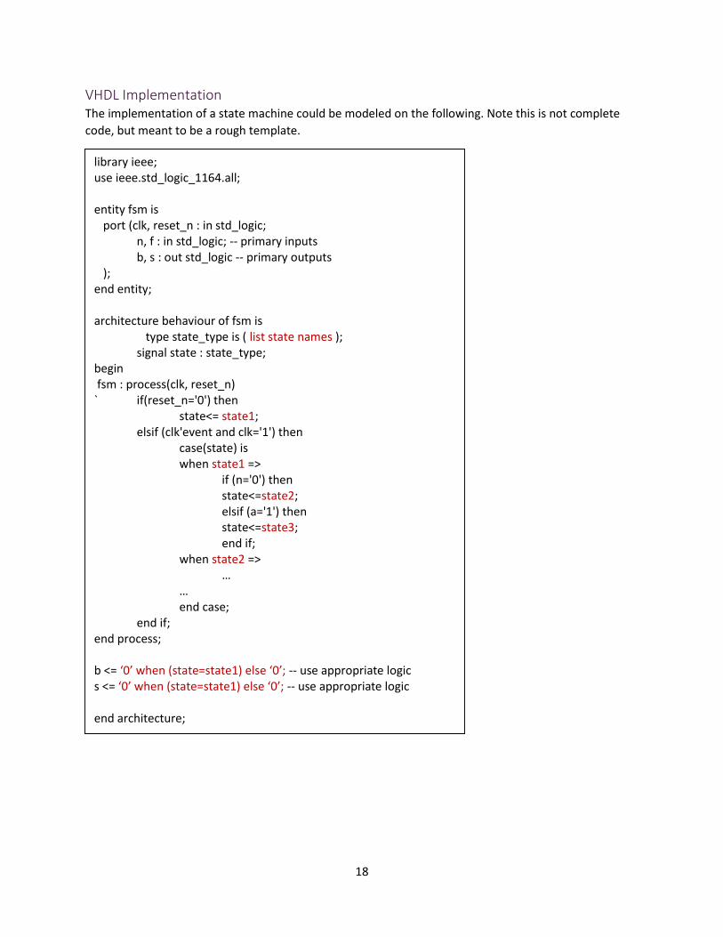
VHDL Implementation The implementation of a state machine could be modeled on the following. Note this is not complete
code, but meant to be a rough template.
library ieee; use ieee.std_logic_1164.all; entity fsm is port (clk, reset_n : in std_logic; n, f : in std_logic; -- primary inputs b, s : out std_logic -- primary outputs ); end entity; architecture behaviour of fsm is
type state_type is ( list state names ); signal state : state_type; begin fsm : process(clk, reset_n) ` if(reset_n='0') then state<= state1; elsif (clk'event and clk='1') then case(state) is when state1 => if (n='0') then state<=state2; elsif (a='1') then state<=state3; end if; when state2 => … … end case; end if; end process; b <= ‘0’ when (state=state1) else ‘0’; -- use appropriate logic s <= ‘0’ when (state=state1) else ‘0’; -- use appropriate logic end architecture;

19
References
[1] Electronics Tutorials, "Laws of Boolean Algebra," Aspen Core, 2016. [Online]. Available:
http://www.electronics-tutorials.ws/boolean/bool_6.html. [Accessed 05 07 2016].
[2] N. Manjikian, C. Hamacher, Z. Vranesic and S. Zaky, Computer Organization and Embedded Systems,
New York: McGraw-Hill, 2012.
[3] N. Manjikian, "Queen's University Exam Bank," 17 12 2012. [Online]. [Accessed 12 08 2016].