Embed Size (px)
Citation preview

Title Engineering Prototype Report for EP-54 – 2.75 W Charger/Adapter Using LNK520P (LinkSwitch)
Specification 85-265 VAC Input, 5.5 V, 500 mA, 2.75 W Output
Application Low Cost Charger / Adapter
Author Power Integrations Applications Department
Document Number EPR-54
Date 07-May-2004
Revision 1.1
Summary and Features
• Low cost, low component count battery charger/adapter – replaces linear transformer based solutions
• Optimized switching characteristics and low-side configuration of LNK520 minimizes EMI - Achieves greater than 10 dBµV margin to composite conducted limits - No Y1 safety capacitor required for EMI compliance - Ultra-low earth leakage current, <5 µA
• Small low cost EE16 transformer - Provision for EE13 transformer for smaller size
• Approximate constant voltage, constant current (CV/CC) primary sensed output characteristic
• Efficiency greater than 65% across all line/load conditions
Power Integrations
5245 Hellyer Avenue, San Jose, CA 95138 USA. Tel: +1 408 414 9200 Fax: +1 408 414 9201
www.powerint.com
The products and applications illustrated herein (including circuits external to the products and transformer construction) may be covered by one or more U.S. and foreign patents or potentially by pending U.S. and foreign patent applications assigned to Power Integrations. A complete list of Power Integrations’ patents may be found at www.powerint.com.

EPR-54 – LinkSwitch 2.75 W Low Cost Charger / Adapter 07-May-2004
Table Of Contents 1 Introduction.................................................................................................................4 2 Power Supply Specification ........................................................................................5 3 Schematic...................................................................................................................6 4 Circuit Description ......................................................................................................7
4.1 Input EMI Filtering ...............................................................................................7 4.2 LinkSwitch Primary and Output Feedback...........................................................7 4.3 Output Rectification .............................................................................................9
5 PCB Layout ................................................................................................................9 6 Bill Of Materials ........................................................................................................10 7 Transformer Specification.........................................................................................11
7.1 Electrical Diagram .............................................................................................11 7.2 Electrical Specifications.....................................................................................11 7.3 Materials............................................................................................................12 7.4 Transformer Build Diagram ...............................................................................13 7.5 Transformer Construction..................................................................................15 7.6 Transformer Bobbing Drawing...........................................................................16
8 Performance Data ....................................................................................................17 8.1 Efficiency ...........................................................................................................17 8.2 No-load Input Power..........................................................................................18 8.3 Regulation .........................................................................................................19
8.3.1 Line and Load ............................................................................................19 8.4 Thermal Performance........................................................................................20
9 Waveforms ...............................................................................................................22 9.1 Drain Voltage and Current, Normal Operation...................................................22 9.2 Output Voltage Start-up Profile (Battery Load) ..................................................22 9.3 Drain Voltage and Current Start-up Profile ........................................................23 9.4 Load Transient Response (75% to 100% Load Step) .......................................24 9.5 Output Ripple Measurements............................................................................25
9.5.1 Ripple Measurement Technique ................................................................25 9.5.2 Ripple Measurement Results .....................................................................26
10 Conducted EMI .....................................................................................................27 11 Appendix A: EE16 Simple Construction................................................................29
11.1 Introduction........................................................................................................29 11.2 Schematic..........................................................................................................29 11.3 Bill of Materials ..................................................................................................29 11.4 Transformer Specification..................................................................................31
11.4.1 Transformer Winding..................................................................................31 11.4.2 Electrical Specifications..............................................................................31 11.4.3 Transformer Build Diagram ........................................................................32
11.5 Performance Data .............................................................................................32 11.5.1 Efficiency....................................................................................................33 11.5.2 Line and Load Regulation ..........................................................................34
11.6 Conducted EMI..................................................................................................34 12 Revision History ................................................................................................36
Page 2 of 40
Power Integrations Tel: +1 408 414 9200 Fax: +1 408 414 9201www.powerint.com

07-May-2004 EPR-54 – LinkSwitch 2.75 W Low Cost Charger / Adapter
Important Note: Although this board is designed to satisfy safety isolation requirements, the engineering prototype has not been agency approved. Therefore, all testing should be performed using an isolation transformer to provide the AC input to the prototype board.
Page 3 of 40
Power IntegrationsTel: +1 408 414 9200 Fax: +1 408 414 9201
www.powerint.com

EPR-54 – LinkSwitch 2.75 W Low Cost Charger / Adapter 07-May-2004
1 Introduction This document is an engineering report describing a 5.5 V, 500 mA charger/adapter power supply. The power supply utilizes the LinkSwitch LNK520 device, optimized for bias winding feedback. The LinkSwitch integrates a 700 V MOSFET, PWM controller, start-up, thermal shut-down, and fault protection circuitry. This power supply is a cost effective replacement of linear transformer based power supplies with the additional features of universal input range and high energy efficiency. Compared to the LNK500, the optimized switching characteristics of the LNK520 and the low-side configuration provides improved EMI performance and less variation in EMI performance from design to design. The document contains the power supply specification, schematic, bill of materials, transformer documentation, printed circuit layout, and performance data.
Figure 1 – Populated Circuit Board Photograph.
An alternate design utilizing simplified EE16 transformer construction is presented. See Appendix A for schematic, construction details and performance curves.
Page 4 of 40
Power Integrations Tel: +1 408 414 9200 Fax: +1 408 414 9201www.powerint.com

07-May-2004 EPR-54 – LinkSwitch 2.75 W Low Cost Charger / Adapter
2 Power Supply Specification Description Symbol Min Typ Max Units Comment
Input Voltage VIN 85 265 VAC 2 Wire – no protective ground. Frequency fLINE 47 50/60 64 Hz No-load Input Power 0.3 W Measured at 230 VAC + 10%
Output Output Voltage VOUT 5.0 5.5 6 V ± 20% (at peak power point) Output Ripple (resistive load) VRIPPLE(R) 300 mV Resistive load (peak power) Output Ripple (battery load) VRIPPLE(B) 150 mV Battery load (peak power) Output Current IOUT 375 500 625 mA ± 25% (at peak power point ) Output Envelope See figure 3
Total Output Power
Continuous Output Power POUT 2.06 2.75 3.43 W
Efficiency η 65 % Measured at POUT (2.75 W), 25 oC
Environmental
Conducted EMI Meets CISPR22B / EN55022B No Y1 Safety Capacitor
Safety Designed to meet IEC950/UL1950 Class II
Surge 2 kV 1.2/50 µs surge, IEC 1000-4-5,
Series Impedance: Differential Mode: 2 Ω Common Mode: 12 Ω
Surge 2 kV 100 kHz ring wave, 500 A short circuit current, differential and
common mode
Ambient Temperature TAMB 0 40 oC In provided enclosure, free convection, sea level
Table 1 - EP54 Power Supply Specification.
Figure 2- EP54 Output Characteristic Specification.
Page 5 of 40
Power IntegrationsTel: +1 408 414 9200 Fax: +1 408 414 9201
www.powerint.com

EPR-54 – LinkSwitch 2.75 W Low Cost Charger / Adapter 07-May-2004
Note: EP-54 is designed for a battery load. If a resistive or electronic load is used the supply may fail to start up at full load. This is normal. To ensure startup into a resistive load, increase the value of C5 to 1 µF (see circuit description for more information).
3 Schematic
Figure 3 – Schematic.
Page 6 of 40
Power Integrations Tel: +1 408 414 9200 Fax: +1 408 414 9201www.powerint.com

07-May-2004 EPR-54 – LinkSwitch 2.75 W Low Cost Charger / Adapter
4 Circuit Description The circuit schematic shown in Figure 3 shows a design that provides a constant voltage / constant current (CV/CC) output characteristic from a universal input voltage range of 85 VAC-265 VAC. This design delivers 2.75 W with nominal peak power point voltage of 5.5 V and a current of 500 mA. The overall operating envelope is shown in Figure 10. The unit provides a CC operating range of ±25% over a case internal temperature range of 25 °C to 65 °C, and a transformer primary inductance tolerance of ±10%. Appendix A details the performance of a simplified EE16 transformer without using foil in the construction. This may be a more attractive design for some magnetics vendors but does result in a slight degradation in the CV regulation. See Appendix A for schematic, transformer construction and performance curves. The PCB layout includes provisions to allow a transformer based on an EE13 bobbin to be fitted. An EE16 core size was selected for this design based on feedback that this is generally the lowest cost core size.
4.1 Input Stage and EMI Filtering The bridge rectifier, D1-D4, rectifies the AC input and is smoothed by C1 and C2, with inductor L1 forming a π-filter to attenuate differential mode conducted EMI. Resistor RF1 is a fusible, flame proof type, providing protection from primary-side short circuits and line surges and provides additional differential EMI filtering. The switching frequency of 42 kHz allows such a simple EMI filter to be used without the need for a Y capacitor while still meeting international EMI standards. It is recommended that RF1 be of wire wound construction to withstand input current surges while the input capacitor charges (metal film type are not recommended), and be compliant with safety flammability hazard requirements. Please consult your safety agency representative for requirements specific to your end-use application. Capacitors C1 and C2 are sized to maintain a minimum DC voltage of around 90 V at the minimum AC input voltage. Their ESR should also be as low as possible to reduce differential mode EMI generation. The value of L1 is selected to give acceptable differential mode EMI attenuation with a current rating to meet the RMS input current at low line (or acceptable temperature rise). Conducted emissions in this design are compliant with EN55022B / CISPR 22B and FCC B limits with no input Y1 safety capacitor.
4.2 LinkSwitch Primary and Output Feedback The LNK520P contains the necessary functions to implement start-up and auto-restart (output protection) operation, output constant voltage (CV) and constant-current (CC) control.
Page 7 of 40
Power IntegrationsTel: +1 408 414 9200 Fax: +1 408 414 9201
www.powerint.com

EPR-54 – LinkSwitch 2.75 W Low Cost Charger / Adapter 07-May-2004
When power is applied, high voltage DC appears at the DRAIN pin of LinkSwitch (U1). The CONTROL pin capacitor C5 is then charged through a switched high voltage current source connected internally between the DRAIN and CONTROL pins. When the CONTROL pin reaches approximately 5.6 V relative to the SOURCE pin, the internal current source is turned off. The internal control circuitry is activated and the high voltage MOSFET starts to switch, using the energy in C5 to power the IC. Once the output has reached regulation, PWM control maintains CV regulation by indirectly sensing the output winding voltage. Ideally the DC output voltage is equal to the bias voltage plus the forward drop of D6B multiplied by the transformer secondary winding to bias winding turns ratio minus the forward drop of D7. However, leakage inductance causes errors that vary with load, causing the output voltage to rise at no-load. To give the best regulation, the bias and secondary windings should be physically close to each other in the transformer. Diode D6B rectifies the output of the bias winding, which is then smoothed by C3 to provide a DC voltage to be fed to the CONTROL pin via R4. Resistor R3 is added to filter noise due to leakage inductance. The value of R4 is set such that, at the peak power point, where the output is still in CV regulation, the CONTROL pin current is approximately 2.2 mA. As the output load is increased, the peak power point (defined by 0.5 × L × I2 × f) is exceeded. The output voltage and therefore primary side bias voltage reduce. The reduction in the bias voltage results in a proportional reduction of CONTROL pin current, which lowers the internal LinkSwitch current limit (current limit control). Constant current (CC) operation controls secondary-side output current by reducing the primary-side current limit. The current limit reduction characteristic has been optimized to maintain an approximate constant output current as the output voltage and bias voltage is reduced. If the load is increased further and the CONTROL pin current falls below approximately 0.8 mA, the CONTROL pin capacitor C5 will discharge and LinkSwitch will enter auto-restart operation. Current limit control removes the need for any secondary-side current sensing components (sense resistor, transistor, optocoupler and associated components). Removing the secondary sense circuit dramatically improves efficiency, giving the associated benefit of reduced enclosure size. Diode D5, C4, R1, and R2 form the primary clamp network. This limits the peak DRAIN voltage due to leakage inductance. Resistor R2 allows the use of a slow, low cost rectifier diode by limiting the reverse current through D5 when U1 turns on. The selection of a slow diode improves radiated EMI and also improves CV regulation, especially at no load.
Page 8 of 40
Power Integrations Tel: +1 408 414 9200 Fax: +1 408 414 9201www.powerint.com

07-May-2004 EPR-54 – LinkSwitch 2.75 W Low Cost Charger / Adapter
4.3 Output Rectification Output rectification is provided by Schottky diode D7. The low forward voltage provides high efficiency across the operating range. Low ESR capacitor C6 achieves minimum output ripple and maximizes operating efficiency.
5 PCB Layout
Figure 4 – EP-54 Printed Circuit Board Layout and Dimensions (0.001 inches)
(note: C7, R5 and R6 are not populated).
Page 9 of 40
Power IntegrationsTel: +1 408 414 9200 Fax: +1 408 414 9201
www.powerint.com

EPR-54 – LinkSwitch 2.75 W Low Cost Charger / Adapter 07-May-2004
6 Bill Of Materials Item Qty Reference Description (Type) P/N, Type Manufacturer 1 1 U1 LinkSwitch LNK520P Power Integrations 2 2 C1, C2 4.7 µF, 400 V (SHD Series)
4.7 µF, 380 V 380VB4R7M8X11C 380VB4R7M8X11L
Sam Young UCC
3 1 C3 1 µF, 50 V, general purpose ECA-1HHG010 Panasonic (or generic) 4 1 C4 330 pF, 1000 V, Ceramic ECK-D3A331KBP Panasonic (or generic) 5 1 C5 220 nF, 50 V, Ceramic Generic 6 1 C6 330 µF, 16 V, 117 mΩ EEU-FC1C331 Panasonic 7 4 D1-4 Rectifier 1 A, 600 V 1N4005, Diodes, Inc. (or generic) 8 1 D5 Rectifier Glass Passivated
1 A, 600 V 1N4007GP, Generic
9 1 D6B 1 A, 600 V, Fast recovery, trr = 200 ns
1N4937 Diodes, Inc. (or generic)
10 1 D7 1 A, 60 V Schottky 11DQ06 International Rectifier (or generic)
11 1 J1 Jumper, 24 AWG, bare (location D6A)
Any
12 1 L1 1.0 mH, 150 mA SBCP-47HY102B Tokin 13 1 RF1 8.2 Ω Fusible CRF0414 253-4/8R2, 5% Vitrohm 14 1 R1 390 kΩ, ¼ W, 5% Any 15 1 R2 100 Ω, 5%, ¼ W Any 16 1 R3 15 Ω, 5%, ½ W Any 17 1 R4 6.81 kΩ (1%), ¼ W Any 18 1 T1 Custom EE16 LSLA40319B-1 L.S.E.
http://www.lishin.com
Page 10 of 40
Power Integrations Tel: +1 408 414 9200 Fax: +1 408 414 9201www.powerint.com

07-May-2004 EPR-54 – LinkSwitch 2.75 W Low Cost Charger / Adapter
7 Transformer Specification Note: To correctly center the output voltage over a junction temperature of 25 °C to 65 °C (approx ambient 0 °C to 40 °C), the design software and design methodology may produce a slightly different transformer design than the one shown here.
7.1 Electrical Diagram
26Sh
1
11
3Shield WDG #1 7
WDG #2 WDG #4
7.2 Electrical Specifica
Electrical Strength Primary Inductance Resonant Frequency
Primary Leakage Inductanc
Page 11 of 40
Primary
T #31 AWG ield & Bias
4
5
00T #32 AWG
2
WDG #3
Figure 5 – Transformer Electrical Diagram
tions
1 second, 60 Hz, from Pins 1-5 to PinPins 1-2, all other windings open, mea100 kHz, 0.4 VRMS Pins 1-2, all other windings open
e Pins 1-2, with Pins 6-7 shorted, meas100 kHz, 0.4 VRMS
Tel: +1 408 414 9
Secondary
33T #32 AWG
68T #30 T.I.W
.
s 6-10 3000 VAC sured at 2.52 mH, +/-10%
400 kHz (Min.) ured at 80 µH (Max.)
Power Integrations
200 Fax: +1 408 414 9201www.powerint.com

EPR-54 – LinkSwitch 2.75 W Low Cost Charger / Adapter 07-May-2004
7.3 Materials
Item Description [1] Core: EE16, PC40EE16 TDK – ALG 252 nH/T2 [2] Bobbin: Horizontal 10 pin (see Section 7.6) [3] Magnet Wire: #32 AWG, Please see note on next page
[4] Foil: Tape Wrapped Copper Foil, 7. 5 mm +/-0.1 mm wide by 0.05 mm/2 mil thick, 35 mm +/- 0.5 mm length – see additional drawing
[5] Triple Insulated Wire: #30 AWG [6] Magnet Wire: #31 AWG, Please see note on next page [7] Tape: 3M 1298 Polyester Film (white) 322 mils (8.2 mm) wide by 2.2 mils thick [8] Tape: 3M 1298 Polyester Film (white) 291 mils (7.4 mm) wide by 2.2 mils thick [9] Tape: 3M 1298 Polyester Film (white) 586 mils (14.9 mm) wide by 2.2 mils thick [10] Tape: 3M 1298 Polyester Film (white) 196 mils (5.0 mm) wide by 2.2 mils thick [11] Barrier Tape: 2.0 mm wide, 0.15 mm thick, Please see the note on the next page [12] Barrier Tape: 2.25 mm wide, 0.15 mm thick, Please see the note on the next page [13] Glue AV118
Note: The transformer is an integral part of the EMI performance of this design. Changes to the transformer, even very minor, may have significant impact on both conducted and radiated EMI. More specific guidance is given below when attempting to repeat this transformer design.
1. Wire gauge selection for core cancellation, secondary and bias windings • The outside diameter of the wire can vary slightly due to variations in the insulation
thickness although the bare copper area diameter is same. • Changing the wire gauge is acceptable to account for overall wire diameter
differences. The wire gauge/size should be selected such that with the specified number of turns the winding completely fills one complete layer.
• The bias winding can have the number of turns varied by up to 2 turns to make a complete layer if necessary but it is preferred to keep the turns as specified.
• Winding information with wire gauge used should be indicated on sample report. 2. Primary winding
• Use the same wire gauge/size as used for the core cancellation winding. 3. Barrier tape
• Transformer vendors may have different thickness of barrier tape. • If the thickness is different, please make the height of the barrier tape the same or
slightly higher than wire thickness used for that winding.
Page 12 of 40
Power Integrations Tel: +1 408 414 9200 Fax: +1 408 414 9201www.powerint.com

07-May-2004 EPR-54 – LinkSwitch 2.75 W Low Cost Charger / Adapter
7.4 Transformer Build Diagram
Wrapped Copper Foil
6Secondary #30 TIW 8T
7
4
Shield & Bias #31 26T
5
4 2 layer Tape
2 layer Tape
2.0 mm Barrier Tape 4 layer each
1st layer: 14T
2.0 mm Barrier Tape 4 Layers
2.25 mm Barrier Tape 4 Layers
2
1
3
Sheild #32 33T
1 layer Tape
4 layer Tape
KEY: = =
Page 13
1
Figure 6a – Transformer Build Diagram.
Electrical phasing
Mechanical start; reversed winding direction or same winding direction with bobbin rotated.
of 40 Power Integrations
Tel: +1 408 414 9200 Fax: +1 408 414 9201www.powerint.com

EPR-54 – LinkSwitch 2.75 W Low Cost Charger / Adapter 07-May-2004
35 mm +/- 0.5 mm
41 mm +/- 0.5 mm
14.9 mm 7.5 mm +/- 0.1 mm
Solder at center, Same height as wire
Magnet wire, Item [3] Tape Item [9]
0.05 mm Thick Copper Foil
Fold
Figure 6b – Foil Construction Diagram.
Page 14 of 40
Power Integrations Tel: +1 408 414 9200 Fax: +1 408 414 9201www.powerint.com

07-May-2004 EPR-54 – LinkSwitch 2.75 W Low Cost Charger / Adapter
7.5 Transformer Construction
Bobbin Preparation Pull Pin 8-10 on bobbin [2] to provide polarization. Set bobbin with pins 1-5 on right hand side.
Shield Winding #1 Start at Pin 1. Wind 33 turns of item [3] from right to left in 1 layer across the entire width of the bobbin.
Basic Insulation Temporarily terminate wire on left hand side of bobbin. Apply 1 layer of tape item [7].
Terminate Shield Winding #1
Terminate item [3] on pin 3. Cut pin 3 below termination to prevent contact with pcb trace.
Basic Insulation (continued)
Apply an additional 3 layers of tape item [7].
Primary Winding #2
Start at pin 2. Wind 100 turns of item [3] in 3 layers, plus 3 to 5 additional turns. Wind uniformly across the entire width of the bobbin with no empty space or gaps in any layer. Finish at pin 1.
Foil Shield
Assemble and apply foil shield [4] starting 3 mm from bottom side of bobbin [2]; such that foil termination wire aligns with pin 4. Insert the foil shield assembly [4] beneath a 10-15 mm long piece of tape (to hold in place). Wrap beneath 1 layer item [7] and terminate foil at pin 4.
Margin Tape Apply 4 layers of item [11] on both sides of the bobbin ensuring no space to either bobbin wall.
Bobbin Preparation Change the bobbin [2] orientation with pins 6-10 on right hand side. Maintain same spindle rotation direction.
Secondary Winding #3
Temporarily start at pin 1. Wind 8 turns item [5] in 1 layer from left to right. Wind uniformly across the entire width of the bobbin with no empty space or gaps in the layer. Finish at pin 7. Remove start from pin 1 and reattach to pin 6.
Basic Insulation Apply 2 layers tape item [7].
Margin Tape L and R
Apply 4 layers of item [11] on left side of the bobbin ensuring no space to bobbin wall. Apply 4 layers of item [12] on right side of the bobbin ensuring no space to bobbin wall.
Bias Winding #4
Start at pin 4. Wind 14 turns item [6] from left to right. Wind uniformly across the entire width of the bobbin with no empty space or gaps in the layer.
Basic Insulation Apply 1 layer of tape item [6], maintaining bias winding exit at edge of margin tape barrier.
Bias Winding #4 (continued)
Continue winding item [6] from right to left. Wind a total of 26 turns item [6]. Finish on pin 5.
Outer Insulation
Apply 2 layers of tape item [7].
Final Assembly Assemble and secure core halves with item [12]. Dip varnish and cure (do not vacuum impregnate).
Page 15 of 40
Power IntegrationsTel: +1 408 414 9200 Fax: +1 408 414 9201
www.powerint.com

EPR-54 – LinkSwitch 2.75 W Low Cost Charger / Adapter 07-May-2004
7.6 Transformer Bobbin Drawing
Page 16 of 40
Power Integrations Tel: +1 408 414 9200 Fax: +1 408 414 9201www.powerint.com

07-May-2004 EPR-54 – LinkSwitch 2.75 W Low Cost Charger / Adapter
8 Performance Data All measurements performed at room temperature, 60 Hz input frequency. Output voltage was measured at the end of the DC output cable. Input power was measured with a Yokogawa WT120 power meter.
8.1 Efficiency Efficiency at Full Load - 0.5A(measured at end of cable)
50%
55%
60%
65%
70%
75%
80%
0 50 100 150 200 250 300
Input Voltage (VAC)
Effic
ienc
y (%
)
Figure 7 - Efficiency vs. Input Voltage, Room Temperature, 60 Hz.
Efficiency vs. Output Current(measured at end of cable)
50%
55%
60%
65%
70%
75%
80%
0 0.1 0.2 0.3 0.4 0.5 0.6
Load Current (A)
Effic
ienc
y (%
)
85 VAC115 VAC190 VAC230 VAC265 VAC
Figure 8 - Efficiency vs. Output Load, Room Temperature, 60Hz.
Page 17 of 40
Power IntegrationsTel: +1 408 414 9200 Fax: +1 408 414 9201
www.powerint.com

EPR-54 – LinkSwitch 2.75 W Low Cost Charger / Adapter 07-May-2004
8.2 No-load Input Power
No-Load Pow
0
0.1
0.2
0.3
0.4
0 50 100 150 200 250 300
Input Voltage (VAC)
Inpu
t Pow
er (W
)
e r Consumption
Figure 9 - Zero Load Input Power vs. Input Line Voltage, Room Temperature, 60 Hz.
Page 18 of 40
Power Integrations Tel: +1 408 414 9200 Fax: +1 408 414 9201www.powerint.com

07-May-2004 EPR-54 – LinkSwitch 2.75 W Low Cost Charger / Adapter
8.3 8.3 Regulation
8.3.1 Line and Load
V/I Characteristics(measured at end of cable)
0
1
2
3
4
5
6
7
8
9
10
11
0 0.1 0.2 0.3 0.4 0.5 0.6 0.7
Load Current (A)
Out
put V
olta
ge (V
DC
)
85 VAC115 VAC190 VAC230 VAC265 VAC
Figure 10 – Load Regulation, Room Temperature, 50 Hz.
Page 19 of 40
Power IntegrationsTel: +1 408 414 9200 Fax: +1 408 414 9201
www.powerint.com

EPR-54 – LinkSwitch 2.75 W Low Cost Charger / Adapter 07-May-2004
8.4 Thermal Performance The thermal images provide detail of the power supply operating component temperatures. The images were recorded after operating the unit for 12 hours at 85 VAC with an output load of 0.5 A at the maximum power point. This provides worst-case temperature rise on the LinkSwitch device. The top image details component temperatures of the assembly with the case removed. Hotspots are visible at LinkSwitch and output diode locations, which reached 53 °C and 66 °C, respectively. Operating within the closed case generated an internal temperature rise of +15 °C. This additional temperature rise gives a maximum LinkSwitch and output diode case temperatures of 68 °C and 81 °C at 24 °C ambient and 93 °C and 106 °C at 50 °C ambient. These results are well within acceptable operating limits.
Page 20 of 40
Power Integrations Tel: +1 408 414 9200 Fax: +1 408 414 9201www.powerint.com

07-May-2004 EPR-54 – LinkSwitch 2.75 W Low Cost Charger / Adapter
LinkSwitch
Lin
Page 21
Output Diode, D7
k
o
Output Diode, D7
Switch
Figure 11 – Thermal Image Measurements of Board and Sealed Adapter, 85 VAC, 5.5 V at 0.5 A, 23 ˚C external ambient.
f 40 Power Integrations
Tel: +1 408 414 9200 Fax: +1 408 414 9201www.powerint.com

EPR-54 – LinkSwitch 2.75 W Low Cost Charger / Adapter 07-May-2004
9 Waveforms 9.1 Drain Voltage and Current, Normal Operation
Figure 12 - 85 VAC, Full Load.
Upper: IDRAIN, 0.1 A / div. Lower: VDRAIN, 100 V, 5 µs / div.
Figure 13 - 265 VAC, Full Load. Upper: IDRAIN, 0.1 A / div. Lower: VDRAIN, 200 V / div, 5 µs / div.
9.2 Output Voltage Start-up Profile (Battery Load) The power supply was started up into an output load simulating a battery. Resistor RLOAD was reduced and confirmed start-up at voltages to 3 V. The battery model included series resistor value of 2.5 Ω (RLOAD) and internal capacitor resistance of 0.5 Ω (RINT_RES). The cable resistance RCABLE was set to zero as the load was attached to the end of the actual output cable.
Figure 14 – Battery load model.
Page 22 of 40
Power Integrations Tel: +1 408 414 9200 Fax: +1 408 414 9201www.powerint.com

07-May-2004 EPR-54 – LinkSwitch 2.75 W Low Cost Charger / Adapter
Figure 15 - Start-up Profile, 85 VAC. 0.5 V, 100 ms / div.
Figure 16 - Start-up Profile, 265 VAC. 0.5 V, 100 ms / div.
9.3 Drain Voltage and Current Start-up Profile
Figure 17 - 85 VAC Input and Maximum Load. Upper: IDRAIN, 0.1 A / div. Lower: VDRAIN, 100 V & 1 ms / div.
Figure 18 - 265 VAC Input and Maximum Load. Upper: IDRAIN, 0.1 A / div. Lower: VDRAIN, 200 V & 1 ms / div.
Page 23 of 40
Power IntegrationsTel: +1 408 414 9200 Fax: +1 408 414 9201
www.powerint.com
EPR-54 – LinkSwitch 2.75 W Low Cost Charger / Adapter 07-May-2004
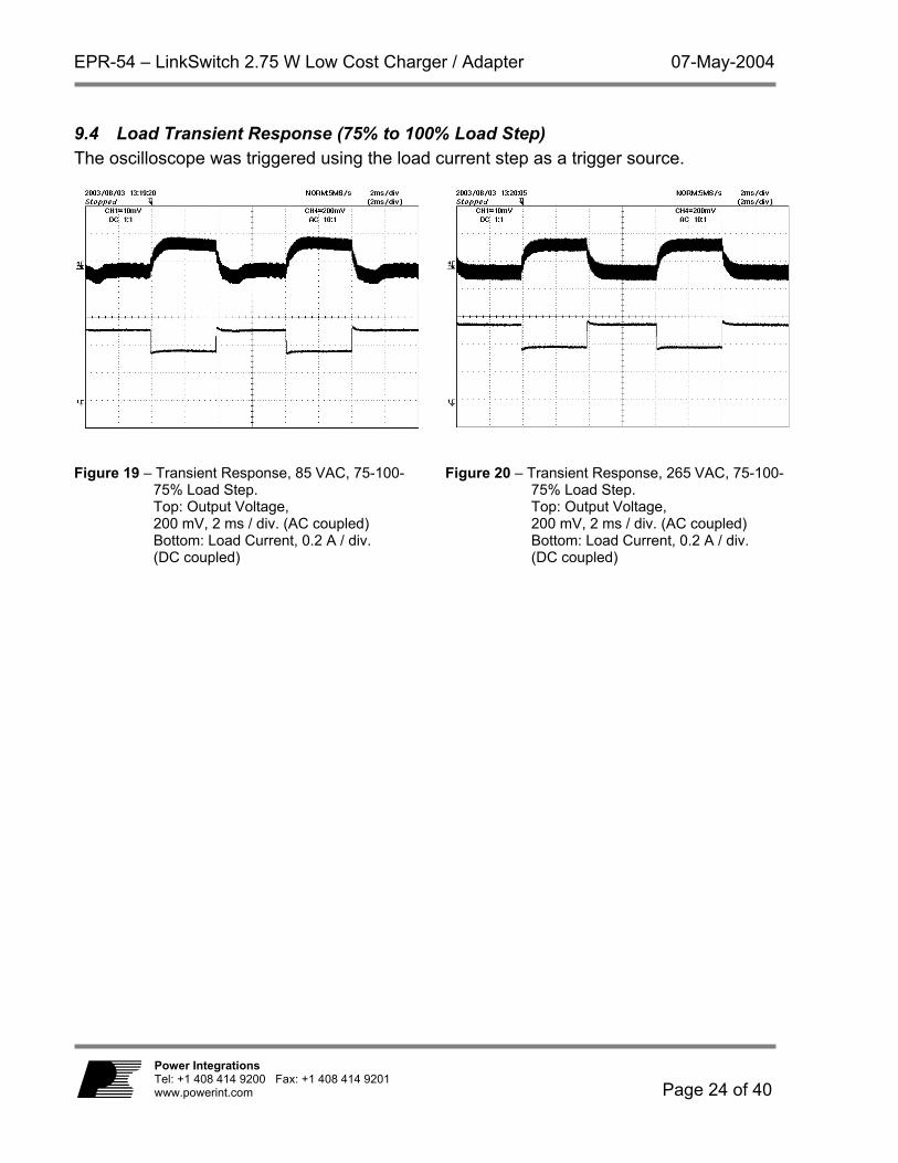
9.4 Load Transient Response (75% to 100% Load Step) The oscilloscope was triggered using the load current step as a trigger source.
Figure 19 – Transient Response, 85 VAC, 75-100-75% Load Step. Top: Output Voltage, 200 mV, 2 ms / div. (AC coupled) Bottom: Load Current, 0.2 A / div. (DC coupled)
Figure 20 – Transient Response, 265 VAC, 75-100-75% Load Step. Top: Output Voltage, 200 mV, 2 ms / div. (AC coupled) Bottom: Load Current, 0.2 A / div. (DC coupled)
Page 24 of 40
Power Integrations Tel: +1 408 414 9200 Fax: +1 408 414 9201www.powerint.com

07-May-2004 EPR-54 – LinkSwitch 2.75 W Low Cost Charger / Adapter
9.5 Output Ripple Measurements
9.5.1 Ripple Measurement Technique For DC output ripple measurements, a modified oscilloscope test probe must be utilized in order to reduce spurious signals due to pickup. Details of the probe modification are provided in Figure 21 and Figure 22. The 5125BA probe adapter is affixed with two capacitors tied in parallel across the probe tip. The capacitors include one (1) 0.1 µF/50 V ceramic type and one (1) 1.0 µF/50 V aluminum electrolytic. The aluminum electrolytic type capacitor is polarized, so proper polarity across DC outputs must be maintained (see below).
Probe Ground
Probe Tip
Figure 21 - Oscilloscope Probe Prepared for Ripple Measurement (End Cap and Ground Lead Removed).
Figure 22 - Oscilloscope Probe with Probe Master 5125BA BNC Adapter (Modified with Wires for Probe
Ground for Ripple Measurement, and Two Parallel Decoupling Capacitors Added).
Page 25 of 40
Power IntegrationsTel: +1 408 414 9200 Fax: +1 408 414 9201
www.powerint.com

EPR-54 – LinkSwitch 2.75 W Low Cost Charger / Adapter 07-May-2004
9.5.2 Ripple Measurement Results All measurements were made with ripple probe at the end of the DC test cable. A resistive load was used in all cases.
Figure 23 - Ripple, 85 VAC, Full Load. 2 ms, 50 mV / div.
Figure 24 - Ripple, 230 VAC, Full Load. 2 ms, 50 mV / div.
Page 26 of 40
Power Integrations Tel: +1 408 414 9200 Fax: +1 408 414 9201www.powerint.com

07-May-2004 EPR-54 – LinkSwitch 2.75 W Low Cost Charger / Adapter
10 Conducted EMI Conducted emissions tests were completed at worst-case conditions: 230 VAC at full load, 5.5 V/0.5 A. Measurements with Artificial Hand connection are less than those with floating DC output load resistor. The output DC cable was included. The test sample exhibits greater than 10 dBµV margin below composite quasi-peak and average limits. This provides adequate margin to variation in transformer EMI characteristics. The results show significant attenuation in high frequency emissions. Composite EN55022B / CISPR22B conducted limits are shown.
Figure 25 - Conducted EMI, 230 VAC, Maximum DC Load,
with Artificial Hand Connected to Output Load.
Page 27 of 40
Power IntegrationsTel: +1 408 414 9200 Fax: +1 408 414 9201
www.powerint.com

EPR-54 – LinkSwitch 2.75 W Low Cost Charger / Adapter 07-May-2004
Figure 26 - Conducted EMI, 230 VAC, Maximum DC Load,
Output Load Floating.
Page 28 of 40
Power Integrations Tel: +1 408 414 9200 Fax: +1 408 414 9201www.powerint.com

07-May-2004 EPR-54 – LinkSwitch 2.75 W Low Cost Charger / Adapter
11 Appendix A: EE16 Simple, No Foil, Construction
11.1 Introduction An alternative design utilizing an EE16 transformer with simplified construction is presented. The transformer uses integral bias and bifilar wound shields. These shields offer effective EMI attenuation with minimum additional transformer complexity. Reduced coupling between bias and secondary windings increases load regulation and no-load output voltage. A secondary snubber is required to reduce high frequency EMI. Efficiency is increased from 66% to 70%, due to a reduction in transformer primary-to-secondary leakage inductance. Appendix A presents schematic, bill of materials, transformer construction details and limited performance curves (including conducted EMI). All specification requirements are identical to those presented in Section 2. Unless specified, the performance of this prototype is similar to those presented earlier; including output ripple, waveforms and thermal performance.
11.2 Schematic The alternative EE16 transformer design is pin compatible with the EP-54 printed circuit board. Bias rectifier (D6B) and jumper (J1) are exchanged to maximize performance of the transformer bias shield. In addition, transformer primary shield (pin 3) is tied to bulk DC return. Component value changes are required to filter the increased leakage spike seen on the primary bias winding. This includes the clamp circuit (R1, C4) and primary bias circuitry (R3, R4). Component additions include secondary snubber circuit (R5, C7) and preload resistor (R6).
11.3 Bill of Materials Highlighted items are changes to previous design Item Qty Reference Description (Type) P/N, Type Manufacturer 1 1 U1 LinkSwitch LNK520P Power Integrations 2 2 C1, C2 4.7 µF, 400 V (SHD Series)
4.7 µF, 380 V 380VB4R7M8X11C 380VB4R7M8X11L
Sam Young UCC
3 1 C3 1 µF, 50 V, general purpose ECA-1HHG010 Panasonic (or generic) 4 1 C4 1000 pF, 1000 V Ceramic Any 5 1 C5 220 nF, 50 V Ceramic Any 6 1 C6 330 µF, 16 V, 117 mΩ EEU-FC1C331 Panasonic 7 1 C7 470 pF, 50 V Ceramic Generic 8 4 D1-4 Rectifier 1 A, 600 V 1N4005 Diodes, Inc. (or generic) 9 1 D5 Rectifier Glass Passivated
1 A, 600 V 1N4007GP Any – generic
10 1 D6A 1 A, 600 V, Fast recovery, trr = 200 ns
1N4937 Diodes, Inc. (or generic)
Page 29 of 40
Power IntegrationsTel: +1 408 414 9200 Fax: +1 408 414 9201
www.powerint.com

EPR-54 – LinkSwitch 2.75 W Low Cost Charger / Adapter 07-May-2004 11 1 D7 1 A, 60 V Schottky 11DQ06 International Rectifier
(or generic) 12 1 J1 Jumper, 24 AWG, bare
(location D6B) Generic
13 1 L1 1.0 mH, 150 mA SBCP-47HY102B Tokin 14 1 RF1 8.2 Ω Fusible CRF0414 253-4/8R2, 5% Vitrohm 15 1 R1 200 kΩ, ¼ W Generic 16 1 R2 100 Ω, ¼ W Generic 17 1 R3 200 Ω, ¼ W Generic 18 1 R4 5.9 kΩ (1%), ¼ W Generic 19 1 R5 51 Ω, ¼ W Generic 20 1 R6 5.1 kΩ, ¼ W Generic 21 1 T1 Custom EE16 SIL6027D HiCal
www.hical.com
Page 30 of 40
Power Integrations Tel: +1 408 414 9200 Fax: +1 408 414 9201www.powerint.com

07-May-2004 EPR-54 – LinkSwitch 2.75 W Low Cost Charger / Adapter
11.4 Transformer Specification
11.4.1 Transformer Winding #3
5
P
Flo
WD #1
WD #3
WD #2
Fig
11.4.2 Electrical Specification
Electrical Strength 60H
Primary Inductance (Pin 1 to Pin 3)
Resonant Frequency Primary Leakage
Inductance
Page 31 of 40
38 T 3 AWG
1
4 7
6
rimary G
11T #28X2
3
ating WD #4
Secondary
110 T #33 AW
2ure 27 – Transformer Electrical DiaAlternate EE16.
s
z 1minute, from Pins 1-5 to Pins 6-7
All windings open
All windings open Pins 6-7 shorted
Tel: +1 408 4
12 T #26 TIW
gram,
3000 VAC
2.73 mH +/- 10%
510 kHz (Min.) 60 µH (Max.)
Power Integrations
14 9200 Fax: +1 408 414 9201www.powerint.com
EPR-54 – LinkSwitch 2.75 W Low Cost Charger / Adapter 07-May-2004
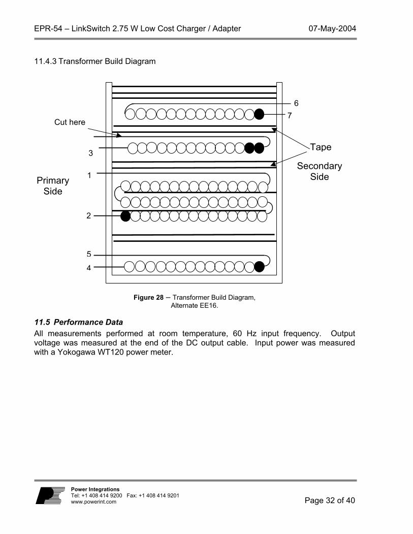
11.4.3 Transformer Build Diagram
2
1
3
Cut here
6
SecondarySide
Tape
7
Primary Side
11.5 PerformAll measuremvoltage was mwith a Yokoga
PoweTel: +www
5
4
Figure 28 – Transformer Build Diagram, Alternate EE16.
ance Data ents performed at room temperature, 60 Hz input frequency. Output easured at the end of the DC output cable. Input power was measured
wa WT120 power meter.
Page 32 of 40 r Integrations 1 408 414 9200 Fax: +1 408 414 9201
.powerint.com

07-May-2004 EPR-54 – LinkSwitch 2.75 W Low Cost Charger / Adapter
11.5.1 Efficiency
Efficiency at Full Load - 0.5 A(measured at end of cable)
50%
55%
60%
65%
70%
75%
80%
0 50 100 150 200 250 300
Input Voltage (VAC)
Effi
cien
cy (%
)y
Figure 29 – Efficiency vs. Input Voltage, Alternate EE16, Full Load, Room Temperature, 60Hz.
Efficiency versus Output Current(measured at end of cable)
50%
55%
60%
65%
70%
75%
80%
0 0.1 0.2 0.3 0.4 0.5 0.6
Load Current (A)
Effic
ienc
y (%
)
85 VAC115 VAC190 VAC230 VAC265 VAC
Figure 30 – Efficiency vs. Output Load, Alternate EE16, Room Temperature, 60Hz.
Page 33 of 40
Power IntegrationsTel: +1 408 414 9200 Fax: +1 408 414 9201
www.powerint.com

EPR-54 – LinkSwitch 2.75 W Low Cost Charger / Adapter 07-May-2004
11.5.2 Line and Load Regulation
V/I Characteristics, Alternate EE16 Transformer(measured at end of cable)
0
1
2
3
4
5
6
7
8
9
10
11
0 0.1 0.2 0.3 0.4 0.5 0.6 0.7
Load Current (A)
Out
put V
olta
ge (V
DC
)
85 VAC115 VAC190 VAC230 VAC265 VAC
Figure 31 – Line and Load Regulation, Alternative EE16 Transformer Design.
11.6 Conducted EMI Conducted emissions were measured at the peak output power point at worst-case nominal line voltage, 230 VAC. Measurements consider both artificial hand (connected to DC output load terminal) and floating outputs. DC cable harness was included. The test sample exhibits greater than 10 dBµV margin below composite Quasi-peak and Average limits. This provides adequate margin to variation in transformer EMI characteristics. The results show significant attenuation in high frequency emissions. Composite EN55022B / CISPR22B conducted limits are shown.
Page 34 of 40
Power Integrations Tel: +1 408 414 9200 Fax: +1 408 414 9201www.powerint.com

07-May-2004 EPR-54 – LinkSwitch 2.75 W Low Cost Charger / Adapter
Figure 32 – Conducted EMI, Alternative EE16 Transformer design, 230 VAC, Maximum DC Load,
with Artificial Hand.
Figure 33 – Conducted EMI, Alternative EE16 Transformer, 230 VAC, Maximum DC Load,
Floating Output.
Page 35 of 40
Power IntegrationsTel: +1 408 414 9200 Fax: +1 408 414 9201
www.powerint.com

EPR-54 – LinkSwitch 2.75 W Low Cost Charger / Adapter 07-May-2004
12 Revision History
Date Author Revision Description & changes 29-Sept-2003 SH 0.1 First Draft 01-Oct-2003 PV 0.2 Second Draft (Edits) 25-Feb-2004 PV 1.0 Third Draft (Photo) 07-May-2004 SH 1.1 Thermal Image (Labels)
Page 36 of 40
Power Integrations Tel: +1 408 414 9200 Fax: +1 408 414 9201www.powerint.com

07-May-2004 EPR-54 – LinkSwitch 2.75 W Low Cost Charger / Adapter
NOTES
Page 37 of 40
Power IntegrationsTel: +1 408 414 9200 Fax: +1 408 414 9201
www.powerint.com

EPR-54 – LinkSwitch 2.75 W Low Cost Charger / Adapter 07-May-2004
NOTES
Page 38 of 40
Power Integrations Tel: +1 408 414 9200 Fax: +1 408 414 9201www.powerint.com

07-May-2004 EPR-54 – LinkSwitch 2.75 W Low Cost Charger / Adapter
NOTES
Page 39 of 40
Power IntegrationsTel: +1 408 414 9200 Fax: +1 408 414 9201
www.powerint.com

EPR-54 – LinkSwitch 2.75 W Low Cost Charger / Adapter 07-May-2004
Power Integrations
Tel: +1 408 414 9200 Fax: +1 408 414 9201
For the latest updates, visit our Web site: www.powerint.com Power Integrations may make changes to its products at any time. Power Integrations has no liability arising from your use of any information, device or circuit described herein nor does it convey any license under its patent rights or the rights of others. POWER INTEGRATIONS MAKES NO WARRANTIES HEREIN AND SPECIFICALLY DISCLAIMS ALL WARRANTIES INCLUDING, WITHOUT LIMITATION, THE IMPLIED WARRANTIES OF MERCHANTABILITY, FITNESS FOR A PARTICULAR PURPOSE, AND NON-INFRINGEMENT OF THIRD PARTY RIGHTS.
PATENT INFORMATION The products and applications illustrated herein (including circuits external to the products and transformer construction) may be covered by one or more U.S. and foreign patents or potentially by pending U.S. and foreign patent applications assigned to Power Integrations. A complete list of Power Integrations’ patents may be found at www.powerint.com. The PI Logo, TOPSwitch, TinySwitch, LinkSwitch, and EcoSmart are registered trademarks of Power Integrations. PI Expert and DPA-Switch are trademarks of Power Integrations. © Copyright 2004, Power Integrations.
Power Integrations Worldwide Sales Support Locations
WORLD HEADQUARTERS 5245 Hellyer Avenue, San Jose, CA 95138, USA Main: +1-408-414-9200 Customer Service: Phone: +1-408-414-9665 Fax: +1-408-414-9765 e-mail: [email protected]
GERMANY Rueckertstrasse 3, D-80336, Munich, Germany Phone: +49-895-527-3910 Fax: +49-895-527-3920 e-mail: [email protected]
JAPAN Keihin-Tatemono 1st Bldg. 12-20 Shin-Yokohama, 2-Chome, Kohoku-ku, Yokohama-shi, Kanagawa 222-0033, Japan Phone: +81-45-471-1021 Fax: +81-45-471-3717 e-mail: [email protected]
TAIWAN 5F-1, No. 316, Nei Hu Rd., Sec. 1 Nei Hu Dist. Taipei, Taiwan 114, R.O.C. Phone: +886-2-2659-4570 Fax: +886-2-2659-4550 e-mail: [email protected]
CHINA (SHANGHAI) Rm 807, Pacheer, Commercial Centre, 555 Nanjing West Road, Shanghai, 200041, China Phone: +86-21-6215-5548 Fax: +86-21-6215-2468 e-mail: [email protected]
INDIA (TECHNICAL SUPPORT) Innovatech 261/A, Ground Floor 7th Main, 17th Cross, Sadashivanagar Bangalore 560080 Phone: +91-80-5113-8020 Fax: +91-80-5113-8023 e-mail: [email protected]
KOREA 8th Floor, DongSung Bldg. 17-8 Yoido-dong, Youngdeungpo-gu, Seoul, 150-874, Korea Phone: +82-2-782-2840 Fax: +82-2-782-4427 e-mail: [email protected]
UK (EUROPE & AFRICA HEADQUARTERS) 1st Floor, St. James’s House East Street Farnham, Surrey GU9 7TJ United Kingdom Phone: +44-1252-730-140 Fax: +44-1252-727-689 e-mail: [email protected]
CHINA (SHENZHEN) Rm# 1705, Bao Hua Bldg. 1016 Hua Qiang Bei Lu, Shenzhen, Guangdong, 518031, China Phone: +86-755-8367-5143 Fax: +86-755-8377-9610 e-mail: [email protected]
ITALY Via Vittorio Veneto 12, Bresso Milano, 20091, Italy Phone: +39-028-928-6001 Fax: +39-028-928-6009 e-mail: [email protected]
SINGAPORE 51 Newton Road, #15-08/10 Goldhill Plaza, Singapore, 308900 Phone: +65-6358-2160 Fax: +65-6358-2015 e-mail: [email protected]
APPLICATIONS HOTLINE World Wide +1-408-414-9660 APPLICATIONS FAX World Wide +1-408-414-9760
Page 40 of 40
www.powerint.com