Embed Size (px)
Citation preview
THÈSE NO 3158 (2004)
ÉCOLE POLYTECHNIQUE FÉDÉRALE DE LAUSANNE
PRÉSENTÉE À LA FACULTÉ SCIENCES DE BASE
Institut de physique des nanostructures
SECTION DE PHYSIQUE
POUR L'OBTENTION DU GRADE DE DOCTEUR ÈS SCIENCES
PAR
M.Sc. in Applied Physics, Delft University of Technlology, Pays-Baset de nationalité néerlandaise
acceptée sur proposition du jury:
Prof. K. Kern, Dr J. Barth, directeurs de thèseDr C. Bosshard, rapporteurProf. J. Brugger, rapporteur
Prof. U. Heiz, rapporteur
Lausanne, EPFL2005
ENGINEERING MOLECULAR NANOSTRUCTURES AT SURFACES
Erik DELVIGNE

i
Abstract
In the framework of this thesis molecular nanostructures have been engineered on
surfaces and are characterized using a variety of techniques. Two types of molecules have been
used: carbon nanotubes (CNT) and 4-[trans-2-(pyrid-4-yl-vinyl)] benzoic acid (PVBA), which
is especially designed for nonlinear optical (NLO) applications and to facilitate self-assembly by
formation of strong H-bonds. Supramolecular NLO thin films of PVBA have been grown on
amorphous glass substrates using Oblique Incidence Organic Molecular Beam Deposition (OI-
OMBD) and molecular self-assembly. The molecular orientation in the films has been
investigated by studying the macroscopic NLO response of the thin films. When deposited on an
atomically clean Cu(100) surface, PVBA molecules assemble into 2D supramolecular
arrangements. The obtained 2D structures have been studied in situ by Scanning Tunneling
Microscopy (STM). For the growth of vertically aligned CNT structures, first microcontact
printing ( CP) has been used to create patterned substrates with ferritin catalyst material,
followed by the catalytic growth of CNTs using Chemical Vapor Deposition (CVD). The CNT
related structures have been studied by electron microscopy.
OI-OMBD is a new approach that delivers noncentrosymmetric organic thin films on
amorphous substrates. We studied how the incidence angle of the molecular beam influences the
noncentrosymmetric ordering of molecules within the PVBA thin films. An optimum incidence
angle was found that lies between 40° and 60° from the substrate normal. These deposition
angles result in films with an optimized NLO coefficient that is independent of the film
thickness. Moreover, these films have lower absorption and a better mechanical stability than
films grown at other deposition angles. By investigating the second harmonic light generation of
the PVBA thin films, we found that there is a first thin layer near the substrate where the
molecules are oriented perpendicular to the substrate, whereas the molecules in the bulk of the
film have a preferential orientation parallel to the substrate. The oblique molecular beam acts as
a small symmetry breaking force, giving the molecules within the plane of the film a
preferential orientation that is a small trend above an equiprobable distribution of orientations.
The present optimization is an important step toward the development of optimized NLO thin
films, by applying the same deposition technique to molecules with a higher hyperpolarizability.
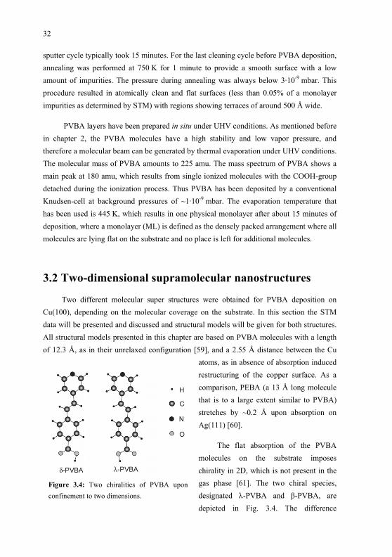
The two-dimensional structures that are formed by PVBA deposited on a Cu(100)
substrate result in two distinct phases: the “Square Structure” (SQS) for low molecular coverage
and the “Butterfly Structure” (BFS) near saturation coverage. In both phases the carboxylic acid
ii
group of the molecules is deprotonated, as demonstrated by XPS measurements. For the SQS,
chiral separation of the PVBA 2D enantiomers takes place to form two distinguishable
enantiomerically pure domain types. A detailed structural analysis suggests H-bonding between
two pyridyl groups and H-bonding involving the carboxylate group. Each carboxylate group
binds to the favored or to the unfavored side of a perpendicularly oriented molecule, in a ratio
that decreases with molecular coverage. In this way the surface density of characteristic open
squares in the SQS can be tuned. For the BFS, the molecular ordering is fundamentally different
from the SQS. In the BFS H-bonding does take place between carboxylate groups and the sides
of molecules, but four pyridyl groups are pushed together at the center of each ‘butterfly’ unit
instead of forming appreciable H-bonding. Furthermore chiral separation is suppressed, leading
to racemic BFS domains. The transition from SQS to the closer packed BFS is driven by space
limitations at high molecular coverages.
Finally, we report the growth of vertically aligned multi-walled CNT structures on
Si/SiO2 substrates, using ferritin as catalyst. The CNTs can be grown at large scale without
encapsulated particles or attached amorphous carbon. They have a very narrow diameter
distribution and their lengths can be controlled by the growth conditions, to several hundreds of
microns and longer. Activation of the ferritin catalyst by oxygen exposure has proven to be
indispensable for the growth of aligned CNTs. The oxygen pressure and the CVD temperature
determine the growth rate, and the CVD duration determines the final CNT length. Nickel and
gold coatings sputtered on CNTs have been studied at different temperatures. Nickel shows a
stronger interaction with the CNT walls than gold, resulting in more homogeneous coatings at
ambient temperature. Surface diffusion at 660° C leads to the formation of larger clusters, which
in case of nickel have a larger contact area with the CNT surface than in case of gold. Inter-CNT
connections have been made by growing CNTs directly on the walls of primary CNTs, using the
formed nickel clusters or ferritin as catalyst. Field emission measurements performed on CNT
samples with secondary CNTs showed clearly improved emission characteristics compared to
samples with only primary CNTs.
iii
Version abrégée
Cette thèse présente une étude de différentes nanostructures moléculaires qui ont été créés
sur des surfaces et caractérisées en utilisant différentes techniques. Deux types de molécules ont
été utilisées: des nanotubes de carbone (CNT) et des molécules de 4-[trans-2-(pyrid-4-yl-vinyl)] benzoic acid (PVBA), laquelle a été élaborée spécialement pour les applications
d’optiques non-linéaire (NLO) et pour faciliter l’auto-assemblage en formant des liaisons
hydrogène fortes entre les molécules. Des couches minces supramoléculaires NLO ont été
réalisées sur un substrat de verre amorphe par déposition par jet moléculaire organique à
incidence oblique (OI-OMBD) ce qui conduit à un auto-assemblage moléculaire. L’orientation
des molécules dans les couches minces a été déterminée en étudiant la réponse macroscopique
NLO des couches. Lorsqu’elles sont déposées sur une surface de Cu(100), les molécules de
PVBA s’assemblent en structures bidimensionnelles, lesquelles sont étudiées in situ par
microscopie à effet tunnel (STM). Afin de créer des structures de CNTs alignés verticalement,
un échantillon de catalyseur de ferritine à d’abord été fabriqué par impression de ferritine par
microcontact ( CP) sur un substrat, puis la croissance des CNTs est obtenue par dépôt en phase
vapeur (CVD). Les structures ainsi crées ont été étudiés par microscopie électronique.
La technique de OI-OMBD est une nouvelle méthode pour créer couches organiques
noncentrosymétriques sur des substrats amorphes. Nous avons étudié comment l’angle
d’incidence du jet moléculaire influence l’organisation des molécules PVBA dans les couches.
Pour un angle de dépôt compris entre 40° et 60° par rapport à la normale du substrat il a été mis
en évidence un coefficient NLO optimal, indépendant de l’épaisseur de la couche. De plus, ces
couches présentent une absorption plus basse et une stabilité mécanique plus grande que
couches formées avec autres angles d’incidence. En étudiant la génération de lumière
correspondant à la deuxième harmonique des couches de PVBA, nous avons montré que dans la
première couche (à l’interface avec le substrat) les molécules sont orientées perpendiculairement
au substrat, alors que les molécules du volume de la couche sont orientées parallèlement par
rapport au substrat. Le jet oblique provoque une orientation préférentielle des molécules (dans le
plan de la couche), laquelle constitue seulement une petite déviation d’une distribution
mathématique équiprobable des orientations des molécules. Cette étude est un pas important
vers le développement de couches NLO optimisées en utilisant molécules avec une
hyperpolarisabilité plus élevée.
iv
Les structures 2D formés par le PVBA déposé sur Cu(100) résultent en deux phases
différentes: la ‘structure carré’ (SQS) pour les bas taux de couverture et la ‘structure papillon’
(BFS) pour une couverture proche de la saturation. Dans les deux phases le groupe
carboxylique de la molécule est déprotoné, ce qui est démontré par des mesures XPS. Pour la
structure SQS on observe une séparation chirale des énantiomères de PVBA, formant deux
types de domaines stéréo-isomériques distincts. Une analyse détaillée des structures suggère la
présence des liaisons hydrogène entre deux groupes pyridyl, et des liaisons hydrogène
concernant la groupe carboxylate. Chaque groupe carboxylate se lie à la coté favorable ou bien
défavorable d’une molécule orientée perpendiculairement, ces deux événements ont des
probabilités qui varient avec le taux de couverture moléculaire. De cette façon la densité des
carrés ouverts – une structure typique pour le SQS – peut être choisi. Pour le BFS, les liaisons
hydrogène se situent entre les groupes carboxylate et les cotés des molécules, mais quatre
groupes pyridyl sont forcés d’être proches dans le centre de chaque structure ‘papillon’ au lieu
de former des liaisons hydrogène fortes. En plus la séparation chirale est supprimée. La
transition de SQS à la plus dense BFS est imposée par limitations d’espace à haute couverture.
Finalement, nous reportons la croissance de structures de CNTs, alignés verticalement sur
des substrats Si/SiO2, avec la ferritine comme catalyseur. Les CNTs ont pu être fabriques sur
une grande échelle sans la présence de particules encapsulés ou de carbone amorphe. Ils ont une
distribution de diamètres très étroite, et leur longueur peut être contrôlée par les conditions de
croissance, jusqu’à plusieurs centaines de microns et plus. L’activation de la ferritine par
exposition à de l’oxygène s’est avérée être indispensable pour la formation de CNTs alignés. La
pression d’oxygène et la température de CVD déterminent le taux de croissance, et la durée de
CVD détermine la longueur finale des CNTs. Des couches de nickel et d’or, déposés sur les
parois des CNTs par dépôt thermique, ont été réalisées et étudiées à différentes températures. Le
nickel montre une interaction plus forte que l’or avec les parois des CNTs. En conséquence les
couches de nickel sont plus homogènes à la température ambiante. La diffusion sur la surface à
une température de 660° C mène à la formation des clusters plus grands, lesquels ont une aire de
contact avec le CNT plus importante dans le cas de nickel par rapport à l’or. Des connexions
entre les CNTs ont été fabriquées en faisant croître des CNTs secondaires directement sur les
parois des CNTs primaires, en utilisant les clusters de nickel ou en utilisant la ferritine comme
catalyseur. Des mesures d’émission de champ, réalisées avec les échantillons présentant des
CNTs secondaires, ont montré une amélioration claire de l’émission d’électrons par rapport aux
échantillons avec seulement des CNTs primaires.
v
Contents
Abstract……………………….….………………………………………………………….i
Version abrégée……………….….…………………………………….….………………iii
Contents……………………….….……………………………..…….….…………………v
1 Introduction…………………..………………………………………….……………….1
2 Self-assembled nonlinear optical thin films by oblique incidence organic molecular
beam deposition……………………………………………………………………..……5
2.1 Experimental…………………………………………………………………….6
2.1.1 Oblique incidence organic molecular beam deposition………….……7
2.1.2 Second Harmonic Generation………………………………..………10
2.2 Optimization and analysis of PVBA thin films………………………………..11
2.2.1 Nonlinear optical coefficient…………………………..…………….12
2.2.2 Molecular orientation in the thin films…………………..…………..15
2.2.3 Absorption……………………………………………….…………..19
2.2.4 Refractive index………………………………………..…………….21
2.2.5 Film stability…………………………………………………………21
2.3 Conclusion…………………………………………………….……………….23
3 Supramolecular assemblies of PVBA on Cu(100)……………….………….……….25
3.1 Experimental………………………………………………………….………..26
3.1.1 Scanning Tunneling Microscopy…………………………………….26
3.1.2 Experimental Setup………………………………..…...…………….30
vi
3.1.3 Sample preparation……………………………………………………31
3.2 Two-dimensional supramolecular nanostructures…………………………..…..32
3.2.1 Low coverage: Square Structure………………………………………33
3.2.2 High coverage: Butterfly Structure………………….…….…………..46
3.3 Conclusion………………………………………………………………………50
4 Carbon nanotube growth and functionalization………………….…….…………….53
4.1 Experimental…………………………………………….…….…….…………..54
4.1.1. Carbon nanotubes……………………………………….……………55
4.1.2 Micro contact printing…………………………………...……………57
4.1.3 Chemical vapor deposition…………………………….…….………..59
4.1.4 Electron Microscopy……………………………………..…………...62
4.1.5 Field emission……………………………………....…………………64
4.2 Vertically aligned carbon nanotubes……………………………………………66
4.2.1 CNT-pillar characterization…………………………….……………..67
4.2.2 Detailed description of CNT-pillar growth……………….…..………72
4.3 Functionalization of nanotubes………………………………….…….….……..81
4.3.1 Metal deposition on nanotubes……………………….….…..………..82
4.3.2 Growth of secondary nanotubes………………………….…..……….88
4.3.3 Field emission with secondary carbon nanotubes……………...……..91
4.4 Conclusion…………………………………………………………….………..94
5 Outlook…………………………………………………….…………………..………..97
Literature……………………………………………………….………….…….………..99
Acknowledgements…………………………………………………………….…..…….109
Chapter 1
Introduction
The term nanotechnology has been used since the mid 1980s to label a vision first described by Richard Feynman in his famous talk “There’s Plenty of Room at the Bottom” [1] [2]. Feynman augured the development of nanodevices that are able to build newnanodevices and other products with atomistic control. Whereas microtechnology and larger scale technologies generally use a top-down approach where the products are machinedmainly using lithographic methods, nanotechnology primarily promotes the bottom-upapproach. In bottom-up nanotechnology the products are constructed by means of molecular recognition and self-assembly, using single atoms or molecules as building blocks. Bottom-up nanotechnology is inspired by nature, which continuously constructs complex, self-organizing and self-regulating molecular machinery and systems for all matter and processes in living organisms. Nowadays the term nanotechnology is used more broadly to describe many types of research where the characteristic dimensions are of the order of 100 nanometers or less.
The construction of complex assemblies using molecular building blocks is paramountfor the development of novel functional materials. The flexibility of molecular engineering makes it possible to synthesize molecules with predictable structure and properties. Self-assembly and self-alignment of these functional molecules can then be used to obtainfunctional materials and supramolecular structures. With the rational-design principle combined with molecular assembly, for instance structures can be created with a tailored pore size and functionality for molecular recognition or gas storage and separation [3] [4] [5]. Regarding electronic miniaturization, molecules that are quantum electronic devices could be designed, synthesized and subsequently assembled into useful circuits by means of self-organized growth and self-alignment. A molecular rectifier has already been proposed
1
2
as early as 1974 [6]. An especially interesting type of molecules for electronic miniaturization are carbon nanotubes, which are rod-shaped single molecules, discovered in 1991 by Iijima [7], with exceptional electronic and mechanical properties. Carbon nanotubes are very promising molecules for the use in molecular electronics, among many other potential applications. They can be used as single-molecule transistors [8] [9] and they are considered for connecting molecular devices and as interconnects on chips [10].
A major question to be tackled is the controlled arrangement of the molecular units. They should be designed in such a way that – next to their primary functionality – they facilitate self-alignment and self-assembly. Hydrogen bonding proved to be particularly important in this respect due to its high selectivity and directionality [11]. Studies of self-assembly processes generate knowledge that is needed to design new molecules and protocols in such a way that predictable architectures can be obtained. On the other hand advanced printing or surface treatment techniques can be used for steering the positioning and orientation of molecular units.
This present work focuses on the creation and characterization of molecular nanostructures on surfaces using a variety of techniques. Two different approaches have been used for the creation of nanostructures. In the first approach, molecules are brought onto a substrate by Organic Molecular Beam Deposition (OMBD), where they assemble into supra-molecular assemblies. The orientation of the molecules and the positions they take in the structures are determined by the self assembly process. The molecules used in this work are especially designed to have intrinsic nonlinear optical properties, to form strong hydrogen bonding and to possess the correct chemical properties for use in OMBD in ultra high vacuum. The second approach employed is the growth of carbon nanotubes from catalyst particles by means of Chemical Vapor Deposition (CVD). The length, diameter and electronic properties of these carbon nanotubes can nowadays be controlled to a certain extent by choosing appropriate fabrication techniques and conditions. The positioning of the nanotubes on the substrate is in our case defined by the microcontact printing ( CP) technique, in which a catalyst material is brought onto the substrate in a predefined pattern, which determines the position where the nanotubes will grow. When CVD is used for nanotube production, a nanotube starts growing on a catalyst particle and grows longer by the constant diffusion of carbon atoms to one end of the nanotube where they keep adding to the nanotube length. In some special cases the nanotube keeps growing during the whole CVD duration and in this way the final length of the nanotube can be chosen by setting the appropriate CVD duration. Techniques have been reported with which the growth direction of the nanotubes can be controlled as well [12] [13] , which is an important step towards the growth of single molecular electronic connections.
INTRODUCTION 3
For the observation and characterization of the molecular nanostructures, Second Harmonic Generation (SHG) has been used and three types of microscopy: Scanning Tunneling Microscopy (STM), Scanning Electron Microscopy (SEM) and Transmission Electron Microscopy (TEM). SHG is used to determine the nonlinear optic response and obtain information about the average molecular ordering in the specific case of supramolecular nonlinear optical materials. With STM, molecular assemblies on conducting substrates can be studied with molecular or even atomic resolution. STM provides unique information about molecular ordering and molecular phenomena at surfaces [14] and is an excellent technique for the study of epitaxial growth on conducting substrates [15]. SEM is an easy-to-use technique for observing a large variety of structures and materials, with a resolution of several nanometers. TEM provides higher resolution than SEM, and moreover the internal structure of e.g. nanotubes can be observed. But TEM can only be used for suspended structures or for structures on electron-transparent substrates.
In chapter 2 of this thesis the formation of nonlinear optical thin films by directed growth is presented, using molecules of 4-[trans-2-(pyrid-4-yl-vinyl)] benzoic acid (PVBA) that have intrinsic second-order nonlinear optical properties and are especially designed for this purpose. PVBA molecules bond to each other in a head-to-tail or tail-to-tail fashion due to hydrogen bonding and in this way assemble into oriented supramolecular structures. For the production of organic nonlinear optical thin films with an in-plane directional order, we used a technique that has recently been developed: Oblique Incidence Organic Molecular Beam Deposition (OI-OMBD) [16] [17] [18]. The macroscopic supramolecular assembly must be noncentrosymmetric, because only in this way the intrinsic second-order nonlinear optical properties of the individual molecules can add up to a macroscopic nonlinearity in the solid state. The PVBA thin films grown by OI-OMBD are noncentrosymmetric because of the symmetry breaking effect of the oblique molecular beam. We investigated the influence of the deposition angle of the molecular beam on the linear and nonlinear optical characteristics of the obtained thin films. In addition, the influence of substrate temperature, deposition rate, and film thickness will be discussed. By measuring the macroscopic second harmonic light generation of the supramolecular thin films, information can be obtained about the optical nonlinearity of the films and about the average molecular ordering in the films. This knowledge increases our understanding of the origin of the self-assembly mechanism that leads to noncentrosymmetric organic thin films in OI-OMBD, and can then be used for making films with larger macroscopic nonlinearity by using improved fabrication methods and new molecules with larger microscopic second-order polarizabilities.
4
In chapter 3 the structures that PVBA molecules form upon deposition on the (100) surface of a Cu crystal have been studied in situ by STM. Whereas the assembly for the nonlinear optical thin films is governed by the beam direction and the intermolecular interactions, the PVBA arrangements on Cu(100) result from a balance of intermolecular interactions and molecule-substrate interactions. Large organic molecules are the basic elements in the field of molecular electronics and knowledge about their behavior at surfaces is thus of high current interest [19]. The PVBA on Cu(100) system shows chiral separation of the two 2D enantiomers of PVBA over mesoscopic distances. This system furthermore shows interesting structural changes of the supramolecular assembly upon variation of the molecular coverage.
The first part of chapter 4 presents a study of the growth of vertically aligned carbon nanotubes where the length of the nanotubes can be controlled by the growth conditions. The CP technique is used to deposit patterns of catalyst containing ink on Si/SiO2
substrates and subsequently the vertically aligned nanotubes are grown on the printed pattern by CVD. We investigated what parameters for CP and CVD lead to respectively vertically aligned nanotubes and arbitrarily oriented nanotubes. Furthermore the influence of the growth parameters on the growth rate and on the reproducibility has been studied. For integration of nanotubes within real devices, good electrical and/or mechanical contacts have to be made either to other nanotubes or to other materials. In the second part of chapter 4, the interaction between nanotubes and metal coatings deposited on the nanotubes is studied and a method for making connections between nanotubes is presented. Cross-linking of nanotubes can be important, e.g., for the creation of nanotube networks for microelectronics. SEM and TEM have been used for the observation and investigation of the aligned nanotube structures, the cross linked nanotubes and the metal-nanotube interactions.
Chapter 2
Self-assembled nonlinear optical thin
films by oblique incidence organic
molecular beam deposition
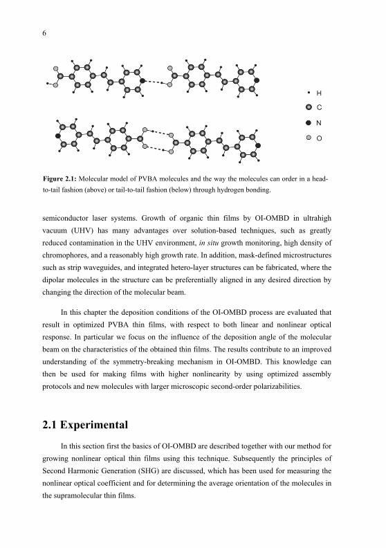
For the production of organic nonlinear optical (NLO) thin films, molecules of 4-trans-2-(pyrid-4-yl-vinyl) benzoic acid (PVBA) have been used, which are dipolar, organicmolecules specifically designed for NLO applications. They consist of a benzoic acid group and a pyridyl group connected through an ethenylene bridge. The molecules are almostplanar and the phenylene and pyridyl rings are aligned parallel. These molecules can bond to each other in a head-to-tail or tail-to-tail fashion due to hydrogen bonding (see Fig. 2.1)and in this way self-assemble into oriented supramolecular structures. Hydrogen bonding between the molecular building blocks can provide high selectivity and directionality [20],which is of key importance for the self-assembly process.
In most of the reported data, dipolar molecules are aligned perpendicular to the substrate, for instance by means of high electric field poling or self-assembly [21]. Only fewexamples of in-plane alignment of dipolar molecules have been described, using methodslike epitaxy on lattice-matched substrate surfaces [22] [23], in-plane electric field poling [24] and Langmuir-Blodgett film deposition [25] [26]. For the production of organic nonlinear optical thin films with an in-plane directional order, we use a technique that has recently been developed: Oblique Incidence Organic Molecular Beam Deposition (OI-OMBD). OI-OMBD provides a new tool for the production of nonlinear optical thin films,which are very attractive, e.g., as components of electro-optical modulators for the telecommunication industry, or as integrated frequency conversion waveguides for
5
6
Figure 2.1: Molecular model of PVBA molecules and the way the molecules can order in a head-to-tail fashion (above) or tail-to-tail fashion (below) through hydrogen bonding.
semiconductor laser systems. Growth of organic thin films by OI-OMBD in ultrahigh vacuum (UHV) has many advantages over solution-based techniques, such as greatly reduced contamination in the UHV environment, in situ growth monitoring, high density of chromophores, and a reasonably high growth rate. In addition, mask-defined microstructuressuch as strip waveguides, and integrated hetero-layer structures can be fabricated, where the dipolar molecules in the structure can be preferentially aligned in any desired direction by changing the direction of the molecular beam.
In this chapter the deposition conditions of the OI-OMBD process are evaluated that result in optimized PVBA thin films, with respect to both linear and nonlinear opticalresponse. In particular we focus on the influence of the deposition angle of the molecularbeam on the characteristics of the obtained thin films. The results contribute to an improved understanding of the symmetry-breaking mechanism in OI-OMBD. This knowledge can then be used for making films with higher nonlinearity by using optimized assemblyprotocols and new molecules with larger microscopic second-order polarizabilities.
2.1 Experimental
In this section first the basics of OI-OMBD are described together with our method forgrowing nonlinear optical thin films using this technique. Subsequently the principles of Second Harmonic Generation (SHG) are discussed, which has been used for measuring the nonlinear optical coefficient and for determining the average orientation of the molecules in the supramolecular thin films.
SELF-ASSEMBLED NONLINEAR OPTICAL THIN FILMS BY OI-OMBD 7
2.1.1 Oblique incidence organic molecular beam deposition
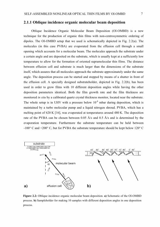
Oblique Incidence Organic Molecular Beam Deposition (OI-OMBD) is a new technique for the production of organic thin films with non-centrosymmetric ordering of dipoles. The OI-OMBD setup that we used is schematically depicted in Fig. 2.2(a). The molecules (in this case PVBA) are evaporated from the effusion cell through a smallopening which accounts for a molecular beam. The molecules approach the substrate under a certain angle and are deposited on the substrate, which is usually kept at a sufficiently low temperature to allow for the formation of oriented supramolecular thin films. The distance between effusion cell and substrate is much larger than the dimensions of the substrate itself, which assures that all molecules approach the substrate approximately under the sameangle. The deposition process can be started and stopped by means of a shutter in front of the effusion cell. A specially designed substrateholder, depicted in Fig. 2.2(b), has been used in order to grow films with 10 different deposition angles while having the other deposition parameters identical. Both the film growth rate and the film thickness aremonitored in situ by a calibrated quartz crystal thickness monitor, located near the substrate.The whole setup is in UHV with a pressure below 10-8 mbar during deposition, which is maintained by a turbo molecular pump and a liquid nitrogen shroud. PVBA, which has amelting point of 620 K [16], was evaporated at temperatures around 480 K. The depositionrate of the PVBA can be chosen between 0.05 Å/s and 0.5 Å/s and is determined by the evaporation temperature. Furthermore the substrate temperature can be held between -100 C and +200 C, but for PVBA the substrate temperature should be kept below 120° C
a) b)
Figure 2.2: Oblique incidence organic molecular beam deposition. a) Schematic of the OI-OMBDprocess. b) Sampleholder for making 10 samples with different deposition angles in one deposition process.
8
in order to avoid desorption of the molecules [17]. The final thickness of the films was measured ex situ by a Tencor Alpha-Step 500 surface profilometer.
The experimental results in this chapter are based on organic supramolecular thin films grown on amorphous glass substrates. The absence of substrate symmetry prevents the substrate from inducing a preferential orientation of the molecules in the film plane.However in-plane film anisotropy is induced by the deposition method. In the OI-OMBD process, the molecular beam is not perpendicular to the substrate but hits the substrate under a certain angle and in a freely chosen direction. The direction of the molecular beamdetermines the direction in which the PVBA molecules in the thin film are aligned.
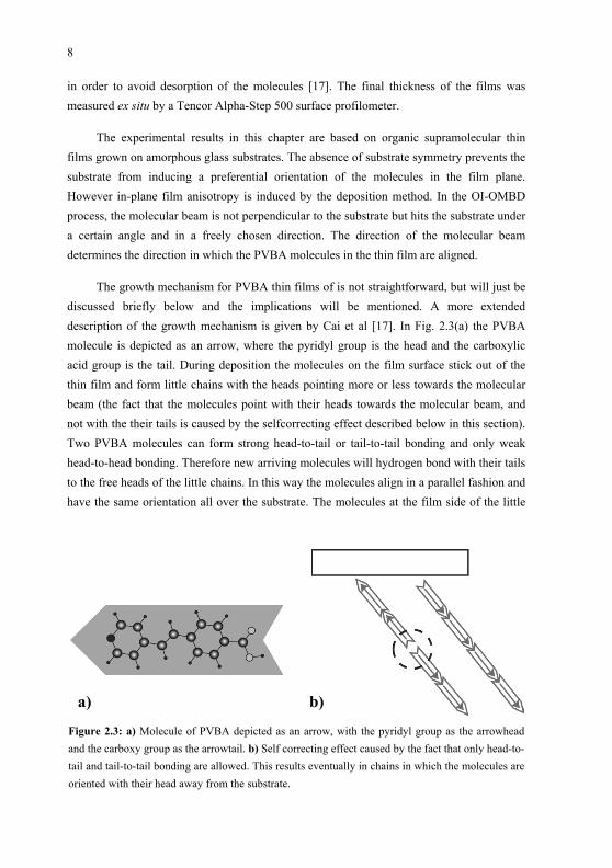
The growth mechanism for PVBA thin films of is not straightforward, but will just be discussed briefly below and the implications will be mentioned. A more extended description of the growth mechanism is given by Cai et al [17]. In Fig. 2.3(a) the PVBA molecule is depicted as an arrow, where the pyridyl group is the head and the carboxylic acid group is the tail. During deposition the molecules on the film surface stick out of the thin film and form little chains with the heads pointing more or less towards the molecularbeam (the fact that the molecules point with their heads towards the molecular beam, and not with the their tails is caused by the selfcorrecting effect described below in this section).Two PVBA molecules can form strong head-to-tail or tail-to-tail bonding and only weak head-to-head bonding. Therefore new arriving molecules will hydrogen bond with their tails to the free heads of the little chains. In this way the molecules align in a parallel fashion and have the same orientation all over the substrate. The molecules at the film side of the little
a) b)
Figure 2.3: a) Molecule of PVBA depicted as an arrow, with the pyridyl group as the arrowhead and the carboxy group as the arrowtail. b) Self correcting effect caused by the fact that only head-to-tail and tail-to-tail bonding are allowed. This results eventually in chains in which the molecules are oriented with their head away from the substrate.
SELF-ASSEMBLED NONLINEAR OPTICAL THIN FILMS BY OI-OMBD 9
chains will lay down parallel to the surface by reforming hydrogen bonds. In the resulting thin film, the PVBA molecules lay flat on the substrate and they are aligned along the projection of the direction of the molecular beam on the substrate. The information from what direction the molecules approached the substrate is preserved because the little chains point in the direction of the molecular beam and the direction of the little chains eventually determines the orientation of the molecules that lay flat in the thin film. The direction in which the molecules are aligned is uniquely determined by the molecular beam direction. It should be noted here that the OMBD process takes place far from thermo-dynamical equilibrium; otherwise dipolar molecules would become anti-parallel due to their dipole moments and the electrostatic interaction [18].
The first molecules on the substrate can point with the head or with the tail end towards the molecular beam, giving rise to anti-parallel chains. But after a few layers all molecules will be oriented in the same direction due to the self-correcting effect explained in Fig. 2.3(b). If molecules stick with their tail out of the thin film, then there is a large chance that tail-to-tail bonding will take place later on in the chain, resulting eventually in a chain with the head sticking out. When the head is sticking out only head-to-tail bonding is possible and the chain will continue with a head sticking out. Of course the growth mechanism described above concerns an ideal film where all molecules are aligned perfectly. In practice the thin film just has an average preferential orientation.
The dipolar molecules in the organic thin film can be preferentially aligned in any desired direction by changing the direction of the molecular beam in situ (or in practice: by turning the substrate around the substrate normal). This allows for instance the growth of oriented films with controllable polar direction both within the plane of the film (by using shadow masks) and within a stack of differently oriented thin films.
The main obstacle for OI-OMBD however lies within the materials. The materials should have a proper vapor pressure and, upon heating, they should sublimate before decomposing in order to be useable for OMBD in UHV. For making thin films that are useful for nonlinear optics, the materials should also have a high stability against orientational randomizing, they should have low scattering losses and they should be able to self assemble in a non-centrosymmetric fashion [16]. Finally the molecules should be composed such that they have an optimized molecular nonlinearity and at the same time are able to form hydrogen bonds.
10
2.1.2 Second Harmonic Generation
Typical organic materials for nonlinear optical effects contain a delocalized -electronsystem and have a donor and an acceptor group [27]. The delocalized -electron system hasa charge distribution that is much more mobile than regular bonds between carbon atoms.Application of an oscillating electric field (with frequency ) to the molecule resultsalternatively in an enhanced charge flow of the electrons towards the acceptor group and a reduced charge flow towards the donor group. The molecule therefore acts as an anharmonic oscillator and will oscillate and emit radiation at frequencies , 2 , 3 etc. The efficiency of the conversion of the fundamental frequency into the second harmonicfrequency is determined by the microscopic second-order polarizability tensor , whichoften has one dominant component along the charge transfer axis. When a film is made out of molecules with a non-zero second-order polarizability and the molecules in the film are aligned in the same direction, then the contributions of the individual molecules will add up to generate second harmonic radiation at a macroscopic level. The contributions of anti-parallel molecules however cancel each other out, making it impossible to observe second-order effects in centrosymmetric materials. Therefore studying the Second HarmonicGeneration (SHG) of various thin films made of identical molecules will give informationabout the average molecular orientation in the thin films. A measure for the macroscopicnonlinearity is given by the nonlinear optical coefficients dIJK, which depend on the second-order polarizability of the individual molecules and on the average orientation of the molecules in the film.
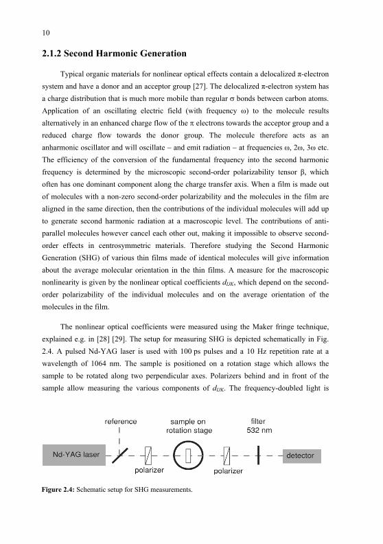
The nonlinear optical coefficients were measured using the Maker fringe technique, explained e.g. in [28] [29]. The setup for measuring SHG is depicted schematically in Fig. 2.4. A pulsed Nd-YAG laser is used with 100 ps pulses and a 10 Hz repetition rate at a wavelength of 1064 nm. The sample is positioned on a rotation stage which allows thesample to be rotated along two perpendicular axes. Polarizers behind and in front of the sample allow measuring the various components of dIJK. The frequency-doubled light is
Figure 2.4: Schematic setup for SHG measurements.
SELF-ASSEMBLED NONLINEAR OPTICAL THIN FILMS BY OI-OMBD 11
filtered out and detected and the data are registered on a computer. Part of the laserbeam is split off before hitting the sample and is used as a reference in order to keep account for the effect of fluctuations in the laser power during the measurements. The SHG intensity of an
-quartz crystal with d111 = 0.3 pm/V was measured in the same setup and used as areference for the determination of the absolute values of the nonlinear optical coefficients of the thin films.
The intensity of the frequency-doubled light, for a laser beam hitting the substrate at the coated side and perpendicular to the substrate, is given by [27]:
2 4 22 2 2 2/ /23 2
2IJK A F S A
o F
2I d L t t I
c n
2
2
(2.1)
where is the refractive index of the film at double frequency, is the coherence length (or the thickness) of the film, is the transmission factor from air to film, t is the transmission factor from substrate to air and is the intensity of the laserbeam.Furthermore the index indicates light of the initial frequency and 2 indicates light of the second harmonic frequency. As one can see there is a quadratic dependence of the SHG intensity on the intensity of the fundamental laserbeam.
Fn L
FAt / / AS
I
From measurements of the SHG intensity of a film and of the quartz reference, thenonlinear optical coefficient can thus be calculated using the following equation:
2 2111
2 22/ /
2 1Q QF c F
IJK QQA F S A
n d l IdL It t
Q Q
2
2
(2.2)
where is the nonlinear optical coefficient of quartz, is the coherence length of quartzat normal incidence,
d111 clQ is a correction for reflection losses of the quartz crystal, is the
measured SHG intensity for the film and is the measured SHG intensity for quartz.FI
QI
2.2 Optimization and analysis of PVBA thin films
The quality of PVBA thin films has been studied with respect to their linear andnonlinear optical properties. The deposition parameters that can be varied in order to optimize the nonlinear optical thin films are the deposition angle ( ), the deposition rate, the
12
substrate temperature and the film thickness. Especially the dependence of the film quality on the deposition angle will be discussed.
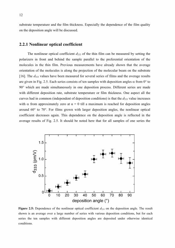
2.2.1 Nonlinear optical coefficient
The nonlinear optical coefficient d333 of the thin film can be measured by setting the polarizers in front and behind the sample parallel to the preferential orientation of themolecules in the thin film. Previous measurements have already shown that the average orientation of the molecules is along the projection of the molecular beam on the substrate [16]. The d333 values have been measured for several series of films and the average resultsare given in Fig. 2.5. Each series consists of ten samples with deposition angles from 0 to 90 which are made simultaneously in one deposition process. Different series are madewith different deposition rate, substrate temperature or film thickness. One aspect all the curves had in common (independent of deposition conditions) is that the d333 value increaseswith from approximately zero at = 0 till a maximum is reached for deposition anglesaround 60 to 70 . For films grown with larger deposition angles, the nonlinear opticalcoefficient decreases again. This dependence on the deposition angle is reflected in the average results of Fig. 2.5. It should be noted here that for all samples of one series the
Figure 2.5: Dependence of the nonlinear optical coefficient d333 on the deposition angle. The result shown is an average over a large number of series with various deposition conditions, but for eachseries the ten samples with different deposition angles are deposited under otherwise identical conditions.
SELF-ASSEMBLED NONLINEAR OPTICAL THIN FILMS BY OI-OMBD 13
deposition time is the same, but the larger the deposition angle the fewer molecules will hit a unit of surface per second. The final film thickness would be expected to be more or less proportional to cos( ) and hence the real deposition rate is expected to be inversely proportional to cos( ). However, the shape of the curve in Fig. 2.5 is caused by the deposition angle and not by the deposition rate, because changing the deposition rate of a whole series does not have a pronounced influence on the nonlinear optical coefficients that are found.
The maximum d333 value obtained is about 1.2 pm/V, which is, as expected, rather low. The pyridyl group and the carboxylic acid group which are chosen for their hydrogen bonding aptitude are relatively weak donor and acceptor groups, leading to a smallmicroscopic second-order polarizability, which is reflected in the small macroscopicnonlinear optical coefficient. But the importance of the incidence angle as the symmetrybreaking force can clearly be seen from the results.
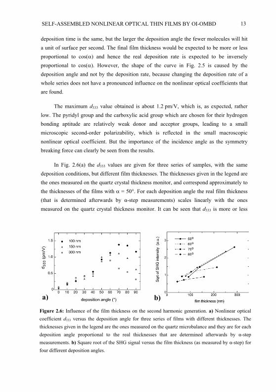
In Fig. 2.6(a) the d333 values are given for three series of samples, with the samedeposition conditions, but different film thicknesses. The thicknesses given in the legend are the ones measured on the quartz crystal thickness monitor, and correspond approximately to the thicknesses of the films with = 50 . For each deposition angle the real film thickness(that is determined afterwards by -step measurements) scales linearly with the ones measured on the quartz crystal thickness monitor. It can be seen that d333 is more or less
a) b)
Figure 2.6: Influence of the film thickness on the second harmonic generation. a) Nonlinear opticalcoefficient d333 versus the deposition angle for three series of films with different thicknesses. Thethicknesses given in the legend are the ones measured on the quartz microbalance and they are for eachdeposition angle proportional to the real thicknesses that are determined afterwards by -stepmeasurements. b) Square root of the SHG signal versus the film thickness (as measured by -step) for four different deposition angles.
14
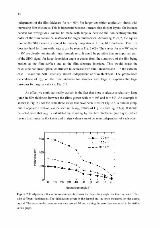
independent of the film thickness for < 60 . For larger deposition angles d333 drops with increasing film thickness. This is important because it means that thicker layers, for instanceneeded for waveguides, cannot be made with large because the non-centrosymmetricorder of the film cannot be sustained for larger thicknesses. According to eq.2, the square root of the SHG intensity should be linearly proportional to the film thickness. That this does not hold for films with large can be seen in Fig. 2.6(b). The curves for = 70 and = 80 are clearly not straight lines through zero. It could be possible that an important part of the SHG signal for large deposition angle comes from the symmetry of the film being broken at the film surface and at the film-substrate interface. This would cause the calculated nonlinear optical coefficient to decrease with film thickness and in the extremecase make the SHG intensity almost independent of film thickness. The pronounced dependence of d333 on the film thickness for samples with large , explains the large errorbars for large values in Fig. 2.5.
An effect we could not really explain is the fact that there is always a relatively largejump in film thickness between the films grown with = 40 and = 50 . An example is shown in Fig. 2.7 for the same three series that have been used for Fig. 2.6. A similar jump,but in opposite direction, can be seen in the d333 values of Fig. 2.5 and Fig. 2.6(a). It shouldbe noted here that d333 is calculated by dividing by the film thickness (see Eq.2), which means that jumps in thickness and in d333 values cannot be seen independent of each other.
Figure 2.7: Alpha-step thickness measurements versus the deposition angle for three series of filmswith different thicknesses. The thicknesses given in the legend are the ones measured on the quartz crystal. The errors in the measurements are around 10 nm, making the error bars too small to be visible is this graph.
SELF-ASSEMBLED NONLINEAR OPTICAL THIN FILMS BY OI-OMBD 15
It seems like part of the material that contributes to the film thickness for 40 does not contribute to the SHG intensity. One hypothesis is that molecules reflect from a substrate or from the substrateholder and end up at the neighboring substrate and hence having a different direction of approaching the substrate than the molecules that are directlydeposited from the molecular beam.
The deposition rate does not manifest a clear influence on the nonlinear optical coefficient d333, at least not below 0.30 Å/s, which was the maximum deposition rate (on the quartz crystal thickness monitor) we used for making the PVBA thin films.
The substrate temperature has no pronounced influence on the d333 values when it iskept below 90 C. Films grown with substrate temperatures above 100° C show very low d333 values and also have really poor optical quality.
2.2.2 Molecular orientation in the thin films
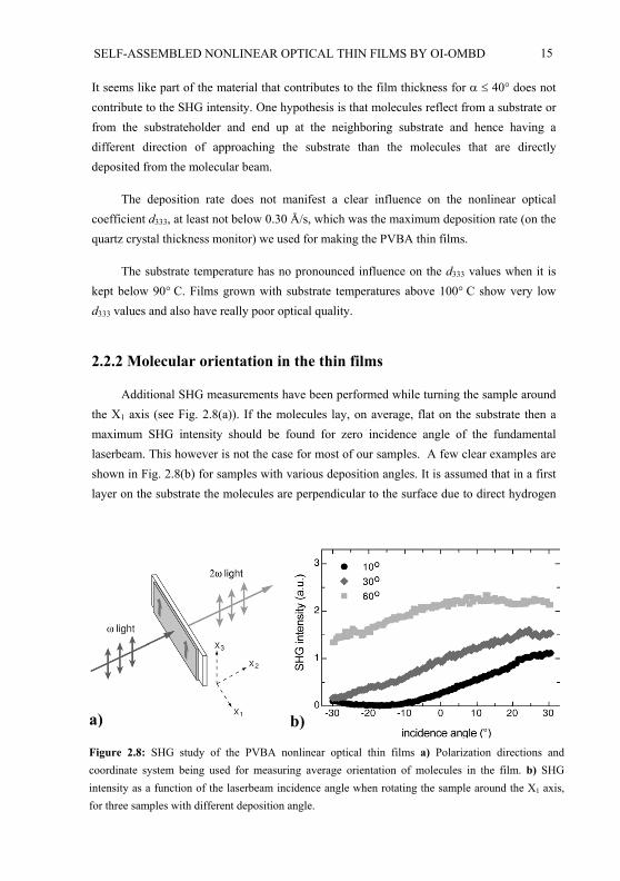
Additional SHG measurements have been performed while turning the sample around the X1 axis (see Fig. 2.8(a)). If the molecules lay, on average, flat on the substrate then a maximum SHG intensity should be found for zero incidence angle of the fundamentallaserbeam. This however is not the case for most of our samples. A few clear examples are shown in Fig. 2.8(b) for samples with various deposition angles. It is assumed that in a first layer on the substrate the molecules are perpendicular to the surface due to direct hydrogen
a) b)
Figure 2.8: SHG study of the PVBA nonlinear optical thin films a) Polarization directions andcoordinate system being used for measuring average orientation of molecules in the film. b) SHGintensity as a function of the laserbeam incidence angle when rotating the sample around the X1 axis,for three samples with different deposition angle.
16
bonding to the substrate whereas the molecules in the bulk of the film are oriented parallelto the substrate [17]. The maxima are always shifted towards positive laserbeam incidenceangle, which in our setup means that the “perpendicular” molecules indeed point with their head away from the substrate. If the laserbeam first goes through the film and then throughthe substrate (film-in-front), then the maximum SHG signal as a function of the laserbeamincidence angle is always found for a larger angle than is the case for film-in-back. This means that the contribution of the “perpendicular” molecules to the total SHG signal is larger for film-in-front than for film-in-back. This effect becomes more pronounced with thicker films and the difference between the positions of the maxima can be up to 20 . In case of film-in-back, the contribution of the “perpendicular” molecules has to travel through the whole film and is partly absorbed on its way. The absorption for light with = 532 nmcan indeed be much larger than for = 1064 nm, especially for thick films. Theseobservations confirm the assumption of having a first few layers of molecules that are perpendicular to the surface. For samples with small or for small film thickness, a minimum rather than a maximum in the SHG signal can be found for small incidence angles of the fundamental laserbeam (e.g. the curve for = 10 in Fig. 2.8(b)). This means that the contribution of the “perpendicular” molecules for these samples is larger than the contribution of the parallel molecules. For samples with around 60 , the maximum of the SHG signal can be found closest to normal incidence angle compared to samples with smaller or larger . This is not surprising since for these samples the total SHG intensity is largest (compared to samples with other deposition angles) and therefore the contribution of the “perpendicular” molecules will be dominated by the contribution from the bulk of the film.
Information about the degree of ordering of the molecules in the thin films can be obtained by comparing the various nonlinear optical coefficients dIJK of the thin film. Using Kleinmann’s symmetry and assuming that the bulk symmetry of the amorphous but preferentially oriented thin film is orthorhombic with point group mm2, the non-vanishing nonlinear optical coefficients are d333, d311 = d131 = d113 and d322 = d232 = d223 [30]. SHG measurements can be performed while rotating the sample around the X1 axis (angle 1) or rotating the sample around the X2 axis (angle 2), where the axes are as defined in Fig.2.8(a). For sample rotation around the X1 axis, the effective nonlinear optical coefficient deff
that determines the SHG intensity is then given as a function of the rotation angle 1 by
31 2 333 1 322 1 1( , 0) cos 3 cos sineffd d d 2 (2.3)
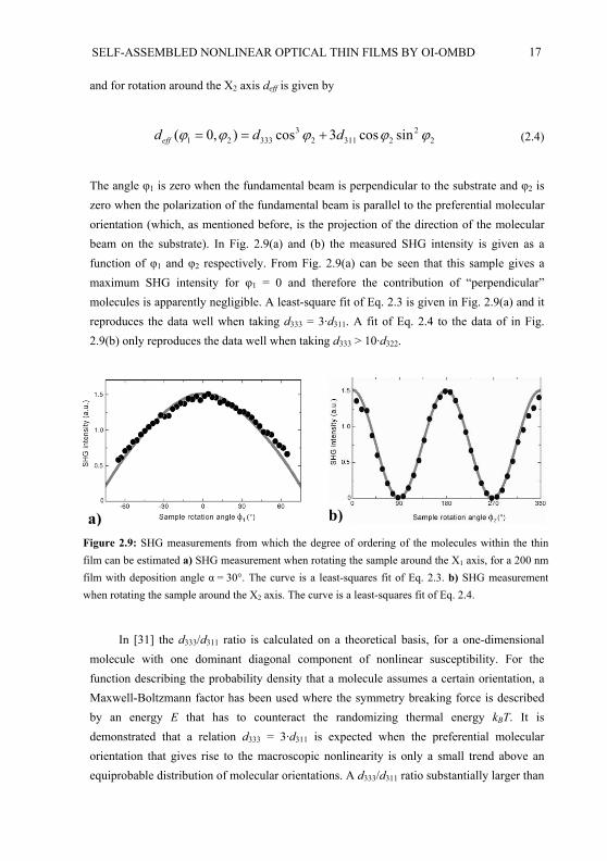
SELF-ASSEMBLED NONLINEAR OPTICAL THIN FILMS BY OI-OMBD 17
and for rotation around the X2 axis deff is given by
3 21 2 333 2 311 2 2( 0, ) cos 3 cos sineffd d d (2.4)
The angle 1 is zero when the fundamental beam is perpendicular to the substrate and 2 iszero when the polarization of the fundamental beam is parallel to the preferential molecular orientation (which, as mentioned before, is the projection of the direction of the molecularbeam on the substrate). In Fig. 2.9(a) and (b) the measured SHG intensity is given as a function of 1 and 2 respectively. From Fig. 2.9(a) can be seen that this sample gives a maximum SHG intensity for 1 = 0 and therefore the contribution of “perpendicular” molecules is apparently negligible. A least-square fit of Eq. 2.3 is given in Fig. 2.9(a) and it reproduces the data well when taking d333 = 3·d311. A fit of Eq. 2.4 to the data of in Fig. 2.9(b) only reproduces the data well when taking d333 > 10·d322.
b)a)Figure 2.9: SHG measurements from which the degree of ordering of the molecules within the thin film can be estimated a) SHG measurement when rotating the sample around the X1 axis, for a 200 nmfilm with deposition angle = 30°. The curve is a least-squares fit of Eq. 2.3. b) SHG measurementwhen rotating the sample around the X2 axis. The curve is a least-squares fit of Eq. 2.4.
In [31] the d333/d311 ratio is calculated on a theoretical basis, for a one-dimensionalmolecule with one dominant diagonal component of nonlinear susceptibility. For thefunction describing the probability density that a molecule assumes a certain orientation, a Maxwell-Boltzmann factor has been used where the symmetry breaking force is described by an energy E that has to counteract the randomizing thermal energy kBT. It is demonstrated that a relation d333 = 3·d311 is expected when the preferential molecularorientation that gives rise to the macroscopic nonlinearity is only a small trend above an equiprobable distribution of molecular orientations. A d333/d311 ratio substantially larger than
18
3 means on the contrary that the preferential molecular orientation is no longer a smalldisturbance [32]. Therefore we can conclude that the direction of the molecular beam onlyacts as a small symmetry breaking force (because d333/d311= 3) giving the molecules in theX3 – X1 plane a small orientational preference along the projection of the direction of the molecular beam on the substrate. The substrate on the contrary induces a larger orientational preference of the molecules in the X3 – X2 plane (because d333/d322 > 10), resulting in apreferential orientation parallel to the substrate.
a)
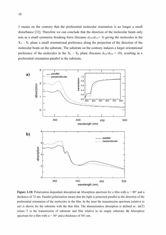
b)
Figure 2.10: Polarization dependant absorption a) Absorption spectrum for a film with = 80 and a thickness of 72 nm. Parallel polarization means that the light is polarized parallel to the direction of the preferential orientation of the molecules in the film. In the inset the transmission spectrum (relative toair) is shown for the substrate with the thin film. The dimensionless absorption is defined as –ln(T) where T is the transmission of substrate and film relative to an empty substrate. b) Absorption spectrum for a film with = 30 and a thickness of 501 nm.
SELF-ASSEMBLED NONLINEAR OPTICAL THIN FILMS BY OI-OMBD 19
2.2.3 Absorption
In Fig. 2.10(a) the absorption spectrum and the transmission spectrum of a PVBA thinfilm are given for two polarizations: light polarized parallel to the molecular preferentialorientation in the film (that means parallel to the charge transfer axis of the molecules) and perpendicular polarized light. The measurements were performed with a SpectrophotometerLambda 9 (Perkin-Elmer). Films of PVBA show an absorption peak at 360 nm. Parallel polarized light results for < 360 nm in a lower absorption – and larger transmission – than perpendicular polarized light. This is in contrast to expectations, since one would expect larger absorption if the oscillating electric field is parallel to the charge transfer axis of the molecule. For wavelengths above 360 nm, the difference between both polarizationsdepends on deposition angle and film thickness. Parallel polarized light always results in a lower absorption in case of large . For smaller parallel polarized light results in larger absorption above 360 nm (see Fig. 2.10(b)). This effect gets stronger for thicker films and, apart from the film thickness, for films with smaller deposition angle. Thick films with small have also rather large absorption for wavelengths far above the absorption peak, up to 900 nm or more.
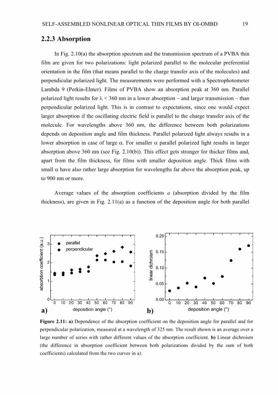
Average values of the absorption coefficients a (absorption divided by the filmthickness), are given in Fig. 2.11(a) as a function of the deposition angle for both parallel
a) b)Figure 2.11: a) Dependence of the absorption coefficient on the deposition angle for parallel and for perpendicular polarization, measured at a wavelength of 325 nm. The result shown is an average over a large number of series with rather different values of the absorption coefficient. b) Linear dichroism(the difference in absorption coefficient between both polarizations divided by the sum of bothcoefficients) calculated from the two curves in a).
20
and perpendicular polarization. The absorption coefficients are measured at = 325 nm because they are large at that wavelength and moreover there is a large difference between the absorption coefficients for the two polarizations. There is a big spread in absorption coefficient for different series of samples, but the deposition angle dependence of all series show basically the same behavior: a increases with for perpendicular polarization and adepends only to a small extend on for parallel polarization, showing a maximum around = 50 - 60 . In Fig. 2.11(a) a jump in absorption coefficient is again present between = 40 and = 50 , which seems to be caused completely by the jump in thickness because measuring the total absorption of each film does not show any jumps.
The curve in Fig. 2.11(a) is strongly influenced by the difference in deposition rate and in film thickness of the ten samples of a given series. It turns out that low deposition rates lead to a smaller absorption below 360 nm but a clearly larger absorption above 360 nm. Moreover it was found that for any given the absorption grows much slower than linearly with the film thickness. It is likely that a large contribution to the total reduction in transmission comes from surface scattering. The surface scattering can also be seen with the naked eye, especially for films grown at low substrate temperatures, manifesting itself in a white color rather than a transparent film. However, transmission measurements performed on samples with different thicknesses and a fixed , did not result in the possibility of determining a constant, thickness independent scattering part and an absorption part growing linearly with film thickness.
The linear dichroism, defined as the difference in absorption coefficient between both polarizations divided by the sum of both coefficients, is given in Fig. 2.11(b) using the same data as in Fig. 2.11(a). The linear dichroism gives an indication of the ordering of the molecules in the film, but it does not make a distinction between parallel and anti-parallel ordering, in contrast to the SHG measurements. The linear dichroism increases with deposition angle for > 50 but for < 40 there is no clear dependence of the linear dichroism on the deposition angle. From an analysis of the integral data set we infer that the dichroism as a function of deposition angle gets steeper with increased film thickness. The dichroism at low decreases with increasing film thickness and at large the dichroism increases. For = 40 - 50 , the linear dichroism is roughly independent of the film thickness.
Low substrate temperature during PVBA deposition seem to cause a larger surface scattering of the thin films, but does not have a clear influence on the linear dichroism.
SELF-ASSEMBLED NONLINEAR OPTICAL THIN FILMS BY OI-OMBD 21
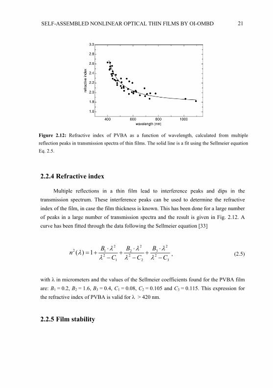
Figure 2.12: Refractive index of PVBA as a function of wavelength, calculated from multiplereflection peaks in transmission spectra of thin films. The solid line is a fit using the Sellmeier equationEq. 2.5.
2.2.4 Refractive index
Multiple reflections in a thin film lead to interference peaks and dips in thetransmission spectrum. These interference peaks can be used to determine the refractiveindex of the film, in case the film thickness is known. This has been done for a large numberof peaks in a large number of transmission spectra and the result is given in Fig. 2.12. A curve has been fitted through the data following the Sellmeier equation [33]
22 22 31 2
2 2 21 2
( ) 1 BB BnC C 3C , (2.5)
with in micrometers and the values of the Sellmeier coefficients found for the PVBA filmare: B1 = 0.2, B2 = 1.6, B3 = 0.4, C1 = 0.08, C2 = 0.105 and C3 = 0.115. This expression forthe refractive index of PVBA is valid for > 420 nm.
2.2.5 Film stability
22
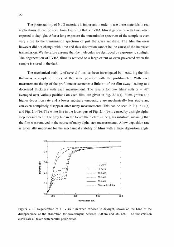
The photostability of NLO materials is important in order to use these materials in real applications. It can be seen from Fig. 2.13 that a PVBA film degenerates with time whenexposed to daylight. After a long exposure the transmission spectrum of the sample is even very close to the transmission spectrum of just the glass substrate. The film thickness however did not change with time and thus desorption cannot be the cause of the increased transmission. We therefore assume that the molecules are destroyed by exposure to sunlight. The degeneration of PVBA films is reduced to a large extent or even prevented when the sample is stored in the dark.
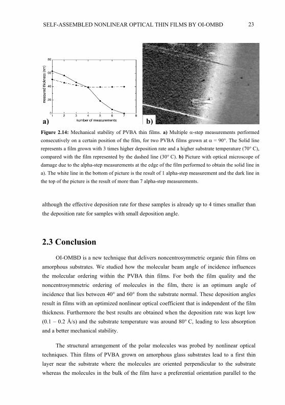
The mechanical stability of several films has been investigated by measuring the filmthickness a couple of times at the same position with the profilometer. With each measurement the tip of the profilometer scratches a little bit of the film away, leading to a decreased thickness with each measurement. The results for two films with = 90 ,averaged over various positions on each film, are given in Fig. 2.14(a). Films grown at a higher deposition rate and a lower substrate temperature are mechanically less stable and can even completely disappear after many measurements. This can be seen in Fig. 2.14(a) and Fig. 2.14(b). The white line in the lower part of Fig. 2.14(b) is caused by a single alpha-step measurement. The grey line in the top of the picture is the glass substrate, meaning that the film was removed in the course of many alpha-step measurements. A low deposition rate is especially important for the mechanical stability of films with a large deposition angle,
Figure 2.13: Degeneration of a PVBA film when exposed to daylight, shown on the hand of the disappearance of the absorption for wavelengths between 300 nm and 360 nm. The transmissioncurves are all taken with parallel polarization.
SELF-ASSEMBLED NONLINEAR OPTICAL THIN FILMS BY OI-OMBD 23
a) b)Figure 2.14: Mechanical stability of PVBA thin films. a) Multiple -step measurements performedconsecutively on a certain position of the film, for two PVBA films grown at = 90 . The Solid line represents a film grown with 3 times higher deposition rate and a higher substrate temperature (70 C), compared with the film represented by the dashed line (30 C). b) Picture with optical microscope of damage due to the alpha-step measurements at the edge of the film performed to obtain the solid line in a). The white line in the bottom of picture is the result of 1 alpha-step measurement and the dark line in the top of the picture is the result of more than 7 alpha-step measurements.
although the effective deposition rate for these samples is already up to 4 times smaller than the deposition rate for samples with small deposition angle.
2.3 Conclusion
OI-OMBD is a new technique that delivers noncentrosymmetric organic thin films on amorphous substrates. We studied how the molecular beam angle of incidence influences the molecular ordering within the PVBA thin films. For both the film quality and the noncentrosymmetric ordering of molecules in the film, there is an optimum angle ofincidence that lies between 40° and 60° from the substrate normal. These deposition angles result in films with an optimized nonlinear optical coefficient that is independent of the filmthickness. Furthermore the best results are obtained when the deposition rate was kept low (0.1 – 0.2 Å/s) and the substrate temperature was around 80 C, leading to less absorptionand a better mechanical stability.
The structural arrangement of the polar molecules was probed by nonlinear opticaltechniques. Thin films of PVBA grown on amorphous glass substrates lead to a first thin layer near the substrate where the molecules are oriented perpendicular to the substratewhereas the molecules in the bulk of the film have a preferential orientation parallel to the

24
The present optimization is an important step toward the development of optimized nonlin
substrate. The initial, perpendicular oriented layer is probably caused by direct hydrogen bonding to the substrate. the direction of the molecular beam acts as a small symmetry breaking force giving the molecules within the plane of the film a preferential orientation (along the projection of the direction of the molecular beam on the substrate) that is only a small trend above an equiprobable distribution of molecular orientations.
ear optical organic thin films. By applying the same design principles and deposition techniques to molecules with a higher hyperpolarizability it should be possible to fabricate useful thin-film waveguides for nonlinear optics and electro-optics.
Chapter 3
Supramolecular assemblies of PVBA
on Cu(100)
The molecular endgroups of PVBA have been especially chosen to form strong hydrogen bonds. As a consequence, substantial attractive interactions between themolecules are also expected when they are adsorbed on a metal surface. Experimentallythese attractive interactions have been observed for PVBA deposited on a Ag(111) substrate [34]. Adsorbed molecules experience the potential energy surface of the substrate, which makes specific adsorption sites energetically favorable. The ease with which molecules can change adsorption positions by either translational or rotational processes (i.e. the surfacemobility) is a key parameter for the creation of supramolecular structures at surfaces.Similarly important is the strength and nature of the intermolecular interactions which compete with the molecule-substrate interactions. As a third parameter, the magnitude of thethermal energy governs the level of ordering which can be achieved. Molecular self-assembly at surfaces is governed by the balance between these forces, which can be tuned via the appropriate choice of adsorbate, substrate material and substrate symmetry.
The supramolecular nanostructures that are studied in this chapter are built up of PVBA molecules, just like the nonlinear optical thin films that were discussed in chapter 2, but now just a monolayer (ML) or less is deposited onto the substrate instead of a thin film.An important difference compared to the thin films (that are grown on amorphous glass substrates) is that upon deposition on an atomically flat Cu(100) crystal, interactionsbetween the molecules and the substrate may become as important as the inter-molecularinteractions. Another marked difference is that the structures presented in this chapter areclose to thermal equilibrium configurations, which is decisive in order to obtain large
25
26
domains of well ordered phases. The thin films of chapter 2, on the contrary, are not in thermal equilibrium, which accounts for their orientational ordering and macroscopic optic nonlinearity.
3.1 Experimental
In this section first the theory and principles of STM will be discussed, which is themethod we used for the analysis of the molecular structures formed by the PVBA molecules on the Cu(100) substrate. In the following the experimental setup is described and the details of the sample preparation are given.
3.1.1 Scanning Tunneling Microscopy
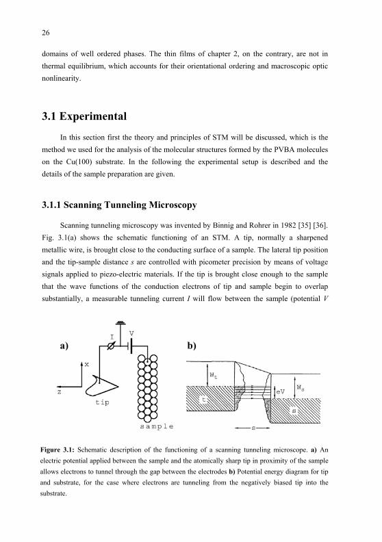
Scanning tunneling microscopy was invented by Binnig and Rohrer in 1982 [35] [36]. Fig. 3.1(a) shows the schematic functioning of an STM. A tip, normally a sharpenedmetallic wire, is brought close to the conducting surface of a sample. The lateral tip positionand the tip-sample distance s are controlled with picometer precision by means of voltage signals applied to piezo-electric materials. If the tip is brought close enough to the samplethat the wave functions of the conduction electrons of tip and sample begin to overlap substantially, a measurable tunneling current I will flow between the sample (potential V
a) b)
Figure 3.1: Schematic description of the functioning of a scanning tunneling microscope. a) Anelectric potential applied between the sample and the atomically sharp tip in proximity of the sampleallows electrons to tunnel through the gap between the electrodes b) Potential energy diagram for tipand substrate, for the case where electrons are tunneling from the negatively biased tip into the substrate.
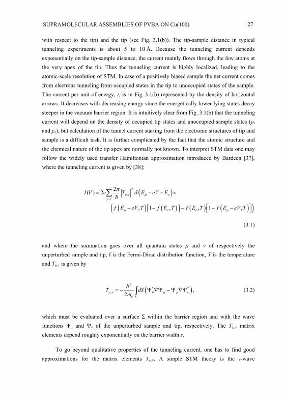
SUPRAMOLECULAR ASSEMBLIES OF PVBA ON Cu(100) 27
with respect to the tip) and the tip (see Fig. 3.1(b)). The tip-sample distance in typicaltunneling experiments is about 5 to 10 Å. Because the tunneling current dependsexponentially on the tip-sample distance, the current mainly flows through the few atoms at the very apex of the tip. Thus the tunneling current is highly localized, leading to the atomic-scale resolution of STM. In case of a positively biased sample the net current comesfrom electrons tunneling from occupied states in the tip to unoccupied states of the sample. The current per unit of energy, i, is in Fig. 3.1(b) represented by the density of horizontal arrows. It decreases with decreasing energy since the energetically lower lying states decaysteeper in the vacuum barrier region. It is intuitively clear from Fig. 3.1(b) that the tunneling current will depend on the density of occupied tip states and unoccupied sample states ( t
and s), but calculation of the tunnel current starting from the electronic structures of tip and sample is a difficult task. It is further complicated by the fact that the atomic structure and the chemical nature of the tip apex are normally not known. To interpret STM data one mayfollow the widely used transfer Hamiltonian approximation introduced by Bardeen [37], where the tunneling current is given by [38]:
2
,,
2( ) 2
, 1 , , 1 ,
I V e T E eV E
f E eV T f E T f E T f E eV T
(3.1)
and where the summation goes over all quantum states and of respectively theunperturbed sample and tip, f is the Fermi-Dirac distribution function, T is the temperatureand T , is given by
2* *
, 2 e
T dSm
, (3.2)
which must be evaluated over a surface within the barrier region and with the wave functions and of the unperturbed sample and tip, respectively. The T , matrixelements depend roughly exponentially on the barrier width s.
To go beyond qualitative properties of the tunneling current, one has to find good approximations for the matrix elements T , . A simple STM theory is the s-wave
28
approximation for tip wave functions introduced by Tersoff and Hamann [39], leading to the following expression for the tunneling current [40] [41]
( , , , , ) ( , , ) ( )
( , , ) , ,
s tI V T x y s dE E x y E eV
Y E V s f E eV T f E T(3.3)
where t is the density of states (DOS) of the tip, s is the Local Density of States (LDOS) of the sample, x and y characterize the lateral position on the sample, and s is the distancebetween tip and sample. An often used expression for the tunneling transmission factor
(E,V,s) is [41]:
2( , , ) exp 2 2e
s tmY E V s s W W E eV (3.4)
where, Ws and Wt are the work functions of sample and tip respectively and V is the electric potential of the sample with respect to the tip (see Fig. 3.1). Although this is a crude simplification, the expressions in Eqs. (3.3) and (3.4) contain the essential and are a good starting point for qualitative and under certain conditions quantitative discussions.
The STM images presented in this chapter are taken in the constant-current imagingmode [42]. In this mode the tunneling current I is compared to a preset current value I0
during the scan. The difference signal I = I - I0 is fed back to the z-piezo voltage in such a way that the tip-sample distance is adjusted to minimize I [43]. The voltage applied to the z-piezo is recorded and forms the STM image. The data obtained in this way represents a surface of constant LDOS of the sample, but one has to be careful to interpret these imagesin terms of surface topography. A well-known counterintuitive example for instance isatomic oxygen chemisorbed on a metal surface, which appears as a depression in STMimages even if the atom is positioned above the metal surface layer [44]. More generally: STM images often show details and internal structures of molecules but the interpretation is not straightforward and a priori it is not even evident whether the bumps are located on the positions of atoms or bonds of the adsorbed molecule.
Before the first successful STM experiments with clearly resolved organic moleculeswere reported [45] [46] [47], it appeared questionable whether “insulating" molecules canbe imaged by STM at all. As stated above, the tunneling current is proportional to the
SUPRAMOLECULAR ASSEMBLIES OF PVBA ON Cu(100) 29
sample LDOS near the Fermi level EF within the framework of the s-wave theory. Most organic molecules have a large energy gap between the highest occupied (HOMO) and the lowest unoccupied (LUMO) molecular orbital. For molecules that are physisorbed on a metal surface, the HOMO- and LUMO-derived resonances are typically several eV below and above EF, respectively. Therefore, the molecule's contribution on the LDOS near EF is rather small and at a first glance one might expect organic molecules to be transparent for tunneling electrons at low bias voltage.
The question what renders STM imaging of “insulating" species possible was first quantitatively discussed by Eigler et al for Xe atoms adsorbed on Ni(110) being imaged as bright 1.6 Å high protrusions [48]. The occupied 5p orbital lies well below EF and the unoccupied 6s orbital lies about 4.5 eV above EF and thus an adsorbed xenon atom makes virtually no contribution to the LDOS at the Fermi level. The electronic structure of an adsorbed Xe atom was calculated using the atom-on-jellium model introduced by Lang [49] [50]. Physisorption causes weak mixing of the Xe 6s state with metal substrate states, resulting in strong broadening of the atomic resonance, but the contribution to the density of states at EF is low and this cannot explain the observed corrugation of Xe atoms in STM. However, the results demonstrated that this resonance extends considerably further out into the vacuum than the bare surface wave functions, which effect makes Xe visible in the STM.
These findings are of general importance for imaging of molecules adsorbed on metal surfaces. Non-resonant tunneling occurs and the contribution of the adsorbate to the current comes from tails of molecular orbital resonances crossing the Fermi level. These tails are usually rather small at the Fermi level, which explains why contributions from the substrate itself cannot be neglected, despite the rather important difference in height. The influence of the substrate becomes evident e.g. for CO chemisorbed on Pt(111) [51] [52], where two different molecular shapes are present in STM topographs employing the same imaging conditions. Bocquet et al. have shown that the different shapes are related to two different chemisorption sites of the molecule on the surface [53], i.e., on top sites and bridge sites.
Among hydrocarbon molecules, the classical example for STM imaging and calculations is certainly benzene. One of the earliest experimental images of this molecule, co-adsorbed with CO on Rh(111) was obtained by Ohtani et al. [45]: The molecule, which is bound at a threefold substrate hollow site [54], appears as three lobes arranged in a triangle in STM topographs. The lobes are located near the center of C C bonds, in between underlying Rh substrate atoms [55]. Hence the STM image of benzene does not show positions of molecular C atoms but some of the C C bonds instead. The shape mainly
30
results from the interaction of the molecule with the threefold substrate site. Benzene does not have any electronic state in resonance with the Fermi level of Rh. The molecularcontrast thus arises again from non-resonant tunneling, i.e., through tails of molecularorbital resonances. As already noticed for Xe, this is the quasi-general case for STM imaging of closed-shell adsorbates.
A detailed description of several theoretical approaches to the contrast mechanism ofadsorbate imaging with STM is given in a review by Sautet [56].
3.1.2 Experimental Setup
For the direct observation of the molecular structures that are presented in this chapter,a variable temperature UHV-STM setup has been used that has been described and used in previous studies [57] [58]. The STM is operational in the 40 K – 800 K temperature rangeand is incorporated in a UHV chamber (base pressure ~2·10-10 mbar), which is equipped with standard surface preparation and analysis tools. Several evaporators for metals and organic molecules can be added. The sample is tightly mounted on the sample holder, cooling is realized with a Helium flux cryostat via a Cu-braid and the sample can be heated by electron bombardment.
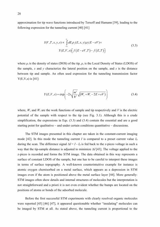
Figure 3.2: Side view of the manipulator and the sample holder. During STM imaging the copper support block is decoupled from the precision tube and rests on the viton-damped Cu-stack. (cf. ref. [57]).
SUPRAMOLECULAR ASSEMBLIES OF PVBA ON Cu(100) 31
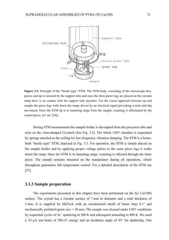
Figure 3.3: Principle of the “beetle type” STM. The STM body, consisting of the microscope disc, piezos and tip is lowered by the support tube and once the three piezo legs are placed on the circularramp there is no contact with the support tube anymore. For the coarse approach between tip andsample the piezo legs walk down the ramp, driven by an electrical signal provoking a stick-and-slip movement. Once the STM tip is in tunneling range from the sample, scanning is effectuated by thecentral piezo. (cf. ref. [58]).
During STM measurement the sample holder is decoupled from the precision tube and rests on the viton-damped Cu-stack (See Fig. 3.2). The whole UHV chamber is suspended by springs attached to the ceiling for low-frequency vibration damping. The STM is a home-built “beetle type" STM, depicted in Fig. 3.3. For operation, the STM is simply placed on the sample holder and by applying proper voltage pulses to the outer piezo legs it walks down the ramp. Once the STM is in tunneling range, scanning is effected through the inner piezo. The sample remains mounted on the manipulator during all operations, which throughout guarantees full temperature control. For a detailed description of the STM see [57].
3.1.3 Sample preparation
The experiments presented in this chapter have been performed on the fcc Cu(100) surface. The crystal has a circular surface of 7 mm in diameter and a total thickness of 3 mm. It is supplied by MaTeck with an orientational misfit of better than 0.1° andmechanically polished (grain size < 30 nm). The sample was cleaned under UHV conditions by sequential cycles of Ar+ sputtering at 300 K and subsequent annealing to 800 K. We used a 10 A ion beam of 500 eV energy and an incidence angle of 45° for sputtering. One
32
sputter cycle typically took 15 minutes. For the last cleaning cycle before PVBA deposition,annealing was performed at 750 K for 1 minute to provide a smooth surface with a low amount of impurities. The pressure during annealing was always below 3·10-9 mbar. Thisprocedure resulted in atomically clean and flat surfaces (less than 0.05% of a monolayerimpurities as determined by STM) with regions showing terraces of around 500 Å wide.
PVBA layers have been prepared in situ under UHV conditions. As mentioned before in chapter 2, the PVBA molecules have a high stability and low vapor pressure, and therefore a molecular beam can be generated by thermal evaporation under UHV conditions.The molecular mass of PVBA amounts to 225 amu. The mass spectrum of PVBA shows amain peak at 180 amu, which results from single ionized molecules with the COOH-group detached during the ionization process. Thus PVBA has been deposited by a conventional Knudsen-cell at background pressures of ~1·10-9 mbar. The evaporation temperature thathas been used is 445 K, which results in one physical monolayer after about 15 minutes of deposition, where a monolayer (ML) is defined as the densely packed arrangement where all molecules are lying flat on the substrate and no place is left for additional molecules.
3.2 Two-dimensional supramolecular nanostructures
Two different molecular super structures were obtained for PVBA deposition on Cu(100), depending on the molecular coverage on the substrate. In this section the STMdata will be presented and discussed and structural models will be given for both structures. All structural models presented in this chapter are based on PVBA molecules with a length of 12.3 Å, as in their unrelaxed configuration [59], and a 2.55 Å distance between the Cu
atoms, as in absence of absorption induced restructuring of the copper surface. As acomparison, PEBA (a 13 Å long moleculethat is to a large extent similar to PVBA) stretches by ~0.2 Å upon absorption on Ag(111) [60].
The flat absorption of the PVBA molecules on the substrate imposeschirality in 2D, which is not present in thegas phase [61]. The two chiral species,designated -PVBA and -PVBA, aredepicted in Fig. 3.4. The difference
Figure 3.4: Two chiralities of PVBA upon confinement to two dimensions.
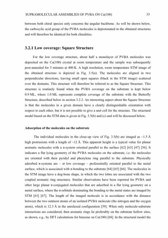
SUPRAMOLECULAR ASSEMBLIES OF PVBA ON Cu(100) 33
between both chiral species only concerns the angular backbone. As will be shown below, the carboxylic acid group of the PVBA molecules is deprotonated in the obtained structures and will therefore be identical for both chiralities.
3.2.1 Low coverage: Square Structure
For the low coverage structure, about half a monolayer of PVBA molecules was deposited on the Cu(100) crystal at room temperature and the sample was subsequently post-annealed for 5 minutes at 400 K. A high resolution, room temperature STM image of the obtained structure is depicted in Fig. 3.5(a). The molecules are aligned in two perpendicular directions, leaving small open squares (black in the STM image) scattered over the domains. This structure will therefore be referred to as the Square Structure. This structure is routinely found when the PVBA coverage on the substrate is kept below 0.9 ML, where 1.0 ML represents complete coverage of the substrate with the Butterfly Structure, described below in section 3.2.2. An interesting aspect about the Square Structure is that the molecules in a given domain have a clearly distinguishable orientation with respect to each other, but it is not possible to give a unit cell for the structure. The structural model based on the STM data is given in Fig. 3.5(b) and (c) and will be discussed below.
Adsorption of the molecules on the substrate
The individual molecules in the close-up view of Fig. 3.5(b) are imaged as ~1.5 Å high protrusions with a length of ~12 Å. This apparent height is a typical value for planar aromatic molecules with a -system oriented parallel to the surface [62] [63] [47] [56]. It indicates a flat lying geometry of the PVBA molecules on the substrate, i.e. the molecules are oriented with their pyridyl and phenylene ring parallel to the substrate. Physically adsorbed -systems are at low coverage preferentially oriented parallel to the metal surface, which is associated with -bonding to the substrate [64] [65] [66]. The molecules in the STM image have a dog-bone shape, in which the two lobes are associated with the two coupled aromatic ring structures. Similar observations have been reported for PVBA and other large planar -conjugated molecules that are adsorbed in a flat lying geometry on a metal surface, where the -orbitals dominating the bonding to the metal states are imaged by STM [63] [67]. The length of the imaged molecule is in accordance with the distance between the two outmost atoms of an isolated PVBA molecule (the nitrogen and the oxygen atom), which is 12.3 Å in the unrelaxed configuration [59]. When only molecule-substrate interactions are considered, then aromatic rings lie preferably on the substrate hollow sites, as shown, e.g., by DFT calculations for benzene on Cu(100) [68]. In the structural model the
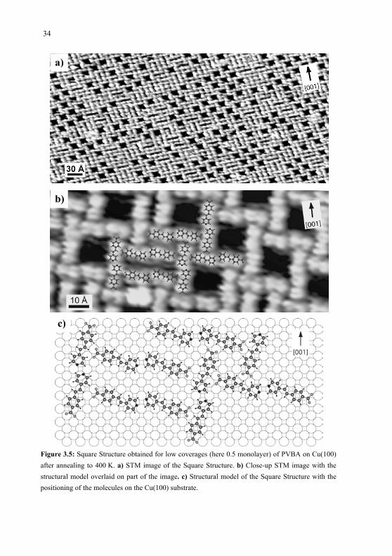
34
a)
b)
c)
Figure 3.5: Square Structure obtained for low coverages (here 0.5 monolayer) of PVBA on Cu(100)after annealing to 400 K. a) STM image of the Square Structure. b) Close-up STM image with thestructural model overlaid on part of the image. c) Structural model of the Square Structure with thepositioning of the molecules on the Cu(100) substrate.
adsorption site of the molecules has therefore been chosen in such a way that at least one of
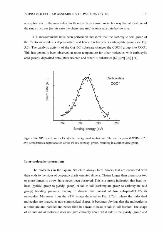
SUPRAMOLECULAR ASSEMBLIES OF PVBA ON Cu(100) 35
adsorption site of the molecules has therefore been chosen in such a way that at least one of the ring structures (in this case the phenylene ring) is on a substrate hollow site.
XPS measurements have been performed and show that the carboxylic acid group of the PVBA molecules is deprotonated, and hence has become a carboxylate group (see Fig. 3.6). The catalytic activity of the Cu(100) substrate changes the COOH group into COO .This has generally been observed at room temperature for other molecules with carboxylicacid groups, deposited onto (100) oriented and other Cu substrates [62] [69] [70] [71].
Figure 3.6: XPS spectrum for O(1s) after background subtraction. The narrow peak (FWHM = 2.0eV) demonstrates deprotonation of the PVBA carboxyl group, resulting in a carboxylate group.
Inter-molecular interactions
The molecules in the Square Structure always form dimers that are connected with their ends to the sides of perpendicularly oriented dimers. Chains longer than dimers, or two or more dimers in a row, have never been observed. This is a strong indication that head-to-head (pyridyl group to pyridyl group) or tail-to-tail (carboxylate group to carboxylate acid group) bonding prevails, leading to dimers that consist of two anti-parallel PVBA molecules. Moreover from the STM image depicted in Fig. 3.7(a), where the individualmolecules are imaged as non-symmetrical shapes, it becomes obvious that the molecules in a dimer are anti-parallel and hence bind in a head-to-head or tail-to-tail fashion. The shape of an individual molecule does not give certainty about what side is the pyridyl group and
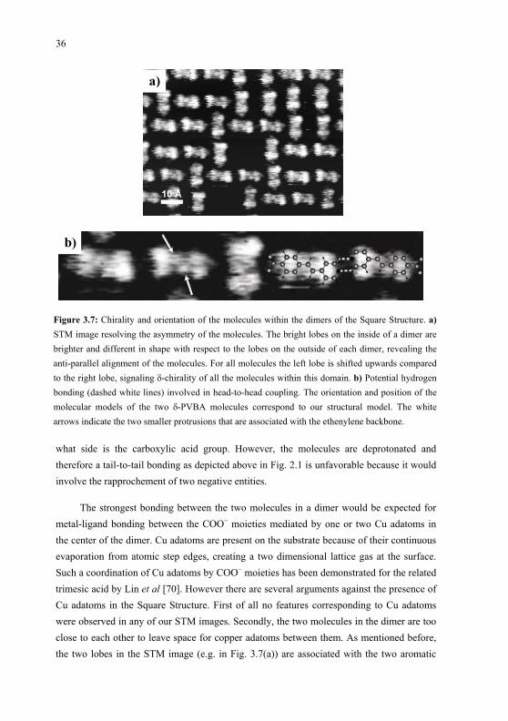
36
a)
b)
Figure 3.7: Chirality and orientation of the molecules within the dimers of the Square Structure. a)STM image resolving the asymmetry of the molecules. The bright lobes on the inside of a dimer arebrighter and different in shape with respect to the lobes on the outside of each dimer, revealing theanti-parallel alignment of the molecules. For all molecules the left lobe is shifted upwards comparedto the right lobe, signaling -chirality of all the molecules within this domain. b) Potential hydrogenbonding (dashed white lines) involved in head-to-head coupling. The orientation and position of themolecular models of the two -PVBA molecules correspond to our structural model. The white arrows indicate the two smaller protrusions that are associated with the ethenylene backbone.
what side is the carboxylic acid group. However, the molecules are deprotonated and therefore a tail-to-tail bonding as depicted above in Fig. 2.1 is unfavorable because it would involve the rapprochement of two negative entities.
The strongest bonding between the two molecules in a dimer would be expected for metal-ligand bonding between the COO moieties mediated by one or two Cu adatoms in the center of the dimer. Cu adatoms are present on the substrate because of their continuousevaporation from atomic step edges, creating a two dimensional lattice gas at the surface.Such a coordination of Cu adatoms by COO moieties has been demonstrated for the relatedtrimesic acid by Lin et al [70]. However there are several arguments against the presence of Cu adatoms in the Square Structure. First of all no features corresponding to Cu adatomswere observed in any of our STM images. Secondly, the two molecules in the dimer are too close to each other to leave space for copper adatoms between them. As mentioned before,the two lobes in the STM image (e.g. in Fig. 3.7(a)) are associated with the two aromatic
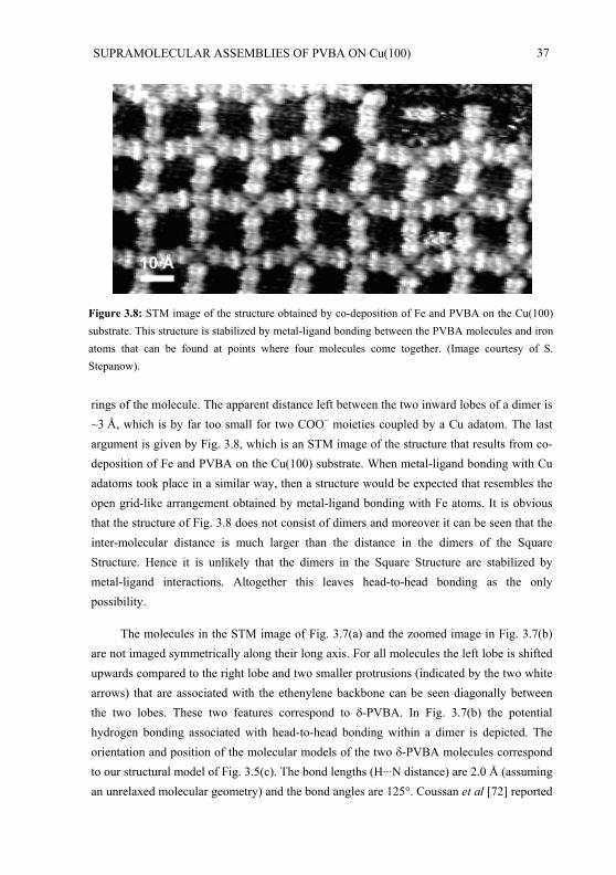
SUPRAMOLECULAR ASSEMBLIES OF PVBA ON Cu(100) 37
Figure 3.8: STM image of the structure obtained by co-deposition of Fe and PVBA on the Cu(100) substrate. This structure is stabilized by metal-ligand bonding between the PVBA molecules and ironatoms that can be found at points where four molecules come together. (Image courtesy of S.Stepanow).
rings of the molecule. The apparent distance left between the two inward lobes of a dimer is~3 Å, which is by far too small for two COO moieties coupled by a Cu adatom. The last argument is given by Fig. 3.8, which is an STM image of the structure that results from co-deposition of Fe and PVBA on the Cu(100) substrate. When metal-ligand bonding with Cu adatoms took place in a similar way, then a structure would be expected that resembles the open grid-like arrangement obtained by metal-ligand bonding with Fe atoms. It is obvious that the structure of Fig. 3.8 does not consist of dimers and moreover it can be seen that the inter-molecular distance is much larger than the distance in the dimers of the SquareStructure. Hence it is unlikely that the dimers in the Square Structure are stabilized by metal-ligand interactions. Altogether this leaves head-to-head bonding as the only possibility.
The molecules in the STM image of Fig. 3.7(a) and the zoomed image in Fig. 3.7(b)are not imaged symmetrically along their long axis. For all molecules the left lobe is shifted upwards compared to the right lobe and two smaller protrusions (indicated by the two white arrows) that are associated with the ethenylene backbone can be seen diagonally between the two lobes. These two features correspond to -PVBA. In Fig. 3.7(b) the potential hydrogen bonding associated with head-to-head bonding within a dimer is depicted. The orientation and position of the molecular models of the two -PVBA molecules correspondto our structural model of Fig. 3.5(c). The bond lengths (H···N distance) are 2.0 Å (assumingan unrelaxed molecular geometry) and the bond angles are 125°. Coussan et al [72] reported
38
DFT calculations for H-bonding in pyridine dimers, resulting in 57 meV bonding energy for the double H-bond, with a 2.6 Å bond length and a 145° bond angle. This bonding energy indicates weak hydrogen bonds, for which the bonding energy decreases relatively slowly with increasing bond length and with decreasing bond angles [73]. The bonding energy for the head-to-head bonding of our PVBA dimers will therefore be in the same regime as the bonding energy for pyridine dimers. Note, however, that the presence of the metal surface electrons may influence the hydrogen bonding for PVBA adsorbed on Cu(100).
Hydrogen bonding may in the Square Structure also be important between the carboxylate group of each molecule and hydrogen atoms at the sides of a perpendicularly oriented molecule (see the structural model in Fig. 3.5(c)). The two oxygen atoms of the carboxylate group form bifurcated hydrogen bonds with in total three hydrogen atoms. The bond lengths (H···O distance) are around 2.0 Å and the bond angles are typically 165°. Other C H···O bonds in literature show bonding energies of 20 to 30 meV for bonding between CH4 and water [73], 78 meV for the two non-identical H-bonds together in 4-methoxybenzaldehyde dimers [74], and 43 meV for C2H4 and water [75]. These values are comparable to – or at least of the same order of magnitude as – the bonding energy for head-to-head bonding. However, the carboxylate groups of the PVBA molecules are formally negative and the resulting hydrogen bonds may be much stronger than the above-mentioned values. Therefore we assume that tail-to-side bonding plays a role in the molecular ordering of the Square Structure that is probably even more important than head-to-head bonding. It should be noted here that additional attractive interactions between the molecules may be present, mediated by the substrate lattice (see e.g., [76]).
Surface mobility
The corrugation of the Cu(100) surface leads to a mobility of the molecules that, at 400 K, is high enough to make the molecules diffuse over the substrate and join other molecules to form supra-molecular structures. The STM images are taken in the constant current mode with typical tunneling currents up to 1 nA and voltages around 1 V, i.e. in the high tunneling resistance regime. The molecules within a domain stay in the same position even when being scanned by the STM tip several times. The domain edges, however, can change in shape with each scan, reflecting a relatively weak molecule-substrate interaction. In case of deposition at room temperature without post-annealing, the mobility of the molecules already suffices to diffuse over the substrate and create small islands that present a metastable precursor for the Square Structure, as can be seen in Fig. 3.9. The islands consist predominantly of dimers that are connected with their ends to the sides of perpendicular dimers, but the islands are rather distorted and relatively small. Moreover
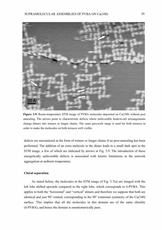
SUPRAMOLECULAR ASSEMBLIES OF PVBA ON Cu(100) 39
Figure 3.9: Room-temperature STM image of PVBA molecules deposited on Cu(100) without postannealing. The arrows point to characteristic defects where unfavorable head-to-tail arreangementschange dimers into trimers or longer chains. The same greyscale range is used for both terraces inorder to make the molecules on both terraces well visible.
defects are encountered in the form of trimers or longer chains if no post-annealing has been performed. The addition of an extra molecule to the dimer leads to a small dark spot in theSTM image, a few of which are indicated by arrows in Fig. 3.9. The introduction of these energetically unfavorable defects is associated with kinetic limitations in the networkaggregation at ambient temperature.
Chiral separation
As stated before, the molecules in the STM image of Fig. 3.7(a) are imaged with the left lobe shifted upwards compared to the right lobe, which corresponds to -PVBA. This applies to both the “horizontal” and “vertical” dimers and therefore we suppose that both are identical and just 90° rotated, corresponding to the 90° rotational symmetry of the Cu(100) surface. This implies that all the molecules in this domain are of the same chirality( -PVBA), and hence the domain is enantiomerically pure.
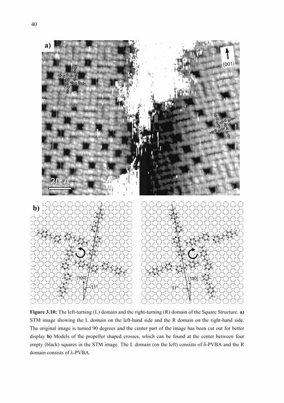
40
a)
b)
Figure 3.10: The left-turning (L) domain and the right-turning (R) domain of the Square Structure. a)STM image showing the L domain on the left-hand side and the R domain on the right-hand side. The original image is turned 90 degrees and the center part of the image has been cut out for betterdisplay b) Models of the propeller shaped crosses, which can be found at the center between four empty (black) squares in the STM image. The L domain (on the left) consists of -PVBA and the R domain consists of -PVBA.
Macroscopically, the surface is still racemic owing to the presence of two mirror
SUPRAMOLECULAR ASSEMBLIES OF PVBA ON Cu(100) 41
Macroscopically, the surface is still racemic owing to the presence of twomirrosymmetric molecular conformations. In Fig. 3.10(a) two Square Structure domains can be seen that are each other’s mirror image. The dimers within the domains are rotated by 22° with respect to each other. We determined (from images with atomic resolution of the Cu substrate) the [001] direction as the mirror axis for the two domains. The fact that the two domains are truly mirror-symmetric, and not rotated versions of each other, is illustratedby the propeller shaped crosses in Fig. 3.10(a) and (b). These crosses, which can be found at the center between four open squares, are always left-turning in the domain on the left hand side and right-turning in the domain on the right hand side of Fig. 3.10(a). Therefore thesetwo domains are designated Left-turning (L) and Right-turning (R) respectively.
In both the L and R domains, each PVBA molecule has the same adsorptionconfiguration, with the phenylene ring on a four-fold hollow site and the nitrogen of thepyridyl unit in near-bridge site. Defining the dimer axis as the line connecting the centers of the phenylene rings of both molecules in the dimer, then the dimers in Fig. 3.10(b) areoriented along the [ 015 ] and [ 051] directions for L domains and along the [ ] and[
0510 15 ] directions for R domains. As a result L domains are turned 11.3° clockwise
compared to the [001] direction and R domains 11.3° counter-clockwise, in good agreementwith the 22° angle we measured between the L and R domain in our STM data. These angles refer to the dimer direction; the molecules make a small angle with the dimerdirection and hence have a different angle with the [001] direction. Since the L and R domain are mirror images, we assume that the molecules in both domains are mirrored aswell. In other words: the L and R domains are each other’s chiral counterpart, where the L domain is build up of -PVBA and the R domain is build up of -PVBA. During depositionthe molecules are adsorbed as both chiral species in a 50/50 ratio, uniformly distributed over the surface. This means that chiral separation of the PVBA 2D enantiomers takes place overmesoscopic distances to form enantiomerically pure domains, facilitated by the high mobility of the molecules at the elevated temperatures employed for the layer preparation.
The fourfold symmetry of the Cu(100) substrate allows in principle for a total of 8 different domains: 2 mirror-symmetric chiralities and both of them can have 4 differentrotated versions. However, two domains that are rotated by 90° or 180° with respect to each other cannot be distinguished from each other since the domains consist of perpendiculardimers, which are built out of two anti-parallel molecules. Therefore the L and R domain are the only two distinguishable varieties of the Square Structure.
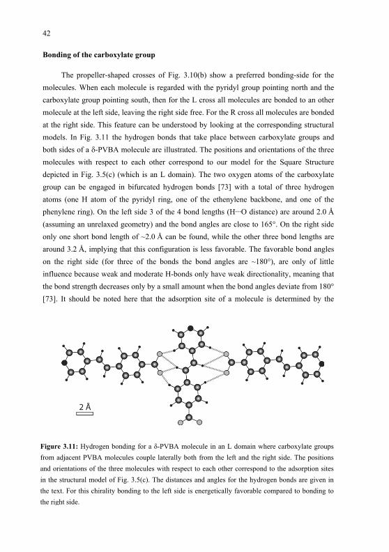
42
Bonding of the carboxylate group
The propeller-shaped crosses of Fig. 3.10(b) show a preferred bonding-side for the molecules. When each molecule is regarded with the pyridyl group pointing north and the carboxylate group pointing south, then for the L cross all molecules are bonded to an other molecule at the left side, leaving the right side free. For the R cross all molecules are bonded at the right side. This feature can be understood by looking at the corresponding structural models. In Fig. 3.11 the hydrogen bonds that take place between carboxylate groups andboth sides of a -PVBA molecule are illustrated. The positions and orientations of the three molecules with respect to each other correspond to our model for the Square Structuredepicted in Fig. 3.5(c) (which is an L domain). The two oxygen atoms of the carboxylate group can be engaged in bifurcated hydrogen bonds [73] with a total of three hydrogen atoms (one H atom of the pyridyl ring, one of the ethenylene backbone, and one of the phenylene ring). On the left side 3 of the 4 bond lengths (H···O distance) are around 2.0 Å(assuming an unrelaxed geometry) and the bond angles are close to 165°. On the right sideonly one short bond length of ~2.0 Å can be found, while the other three bond lengths are around 3.2 Å, implying that this configuration is less favorable. The favorable bond angles on the right side (for three of the bonds the bond angles are ~180°), are only of little influence because weak and moderate H-bonds only have weak directionality, meaning that the bond strength decreases only by a small amount when the bond angles deviate from 180°[73]. It should be noted here that the adsorption site of a molecule is determined by thebalance b
Figure 3.11: Hydrogen bonding for a -PVBA molecule in an L domain where carboxylate groups from adjacent PVBA molecules couple laterally both from the left and the right side. The positionsand orientations of the three molecules with respect to each other correspond to the adsorption sites in the structural model of Fig. 3.5(c). The distances and angles for the hydrogen bonds are given in the text. For this chirality bonding to the left side is energetically favorable compared to bonding tothe right side.
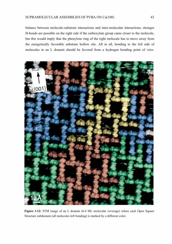
SUPRAMOLECULAR ASSEMBLIES OF PVBA ON Cu(100) 43
balance between molecule-substrate interactions and inter-molecular interactions; stronger H-bonds are possible on the right side if the carboxylate group came closer to the molecule,but this would imply that the phenylene ring of the right molecule has to move away from the energetically favorable substrate hollow site. All in all, bonding to the left side of molecules in an L domain should be favored from a hydrogen bonding point of view.
Figure 3.12: STM image of an L domain (0.4 ML molecular coverage) where each Open SquareStructure subdomain (all molecules left bonding) is marked by a different color.
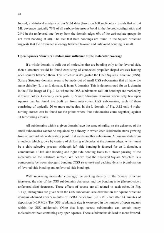
44
Indeed, a statistical analysis of our STM data (based on 600 molecules) reveals that at 0.4 ML coverage typically 76% of all carboxylate groups bond in the favored configuration and 24% in the unfavored one (away from the domain edges 0% of the carboxylate groups do not form bonding at all). The fact that both bondings are found in the Square Structure suggests that the difference in energy between favored and unfavored bonding is small.
Open Squares Structure subdomains: influence of the molecular coverage
If a whole domain is built out of molecules that are bonding only to the favored side, then a structure would be found consisting of connected propeller-shaped crosses leaving open squares between them. This structure is designated the Open Squares Structure (OSS). Square Structure domains seem to be made out of small OSS subdomains that all have the same chirality (L in an L domain, R in an R domain). This is demonstrated for an L domain in the STM image of Fig. 3.12, where the OSS subdomains (all left bonding) are marked by different colors. Generally even parts of Square Structure domains where only few open squares can be found are built up from interwoven OSS subdomains, each of them consisting of typically 20 or more molecules. In the L domain of Fig. 3.12 only 4 right-turning crosses can be found (at the points where four subdomains come together) against 31 left-turning crosses.
All subdomains within a given domain have the same chirality, so the existence of the small subdomains cannot be explained by a theory in which each subdomain starts growing from an individual condensation point till it meets another subdomain. A domain starts from a nucleus which grows by capture of diffusing molecules at the domain edges, which must be a chiro-selective process. Although left side bonding is favored for an L domain, a combination of left side bonding and right side bonding leads to a closer packing of the molecules on the substrate surface. We believe that the observed Square Structure is a compromise between strongest bonding (OSS structure) and packing density (combination of favored-side bonding and unfavored-side bonding).
With increasing molecular coverage, the packing density of the Square Structure increases, the size of the OSS subdomains decreases and the bonding ratio (favored-side : unfavored-side) decreases. These effects of course are all related to each other. In Fig. 3.13(a) histograms are given with the OSS subdomain size distribution for Square Structure domains obtained after 5 minutes of PVBA deposition (~0.3 ML) and after 14 minutes of deposition (~0.9 ML). The OSS subdomain size is expressed in the number of open squares within the OSS subdomain. (Note that long, narrow subdomains can contain many molecules without containing any open squares. These subdomains do lead to more favored-
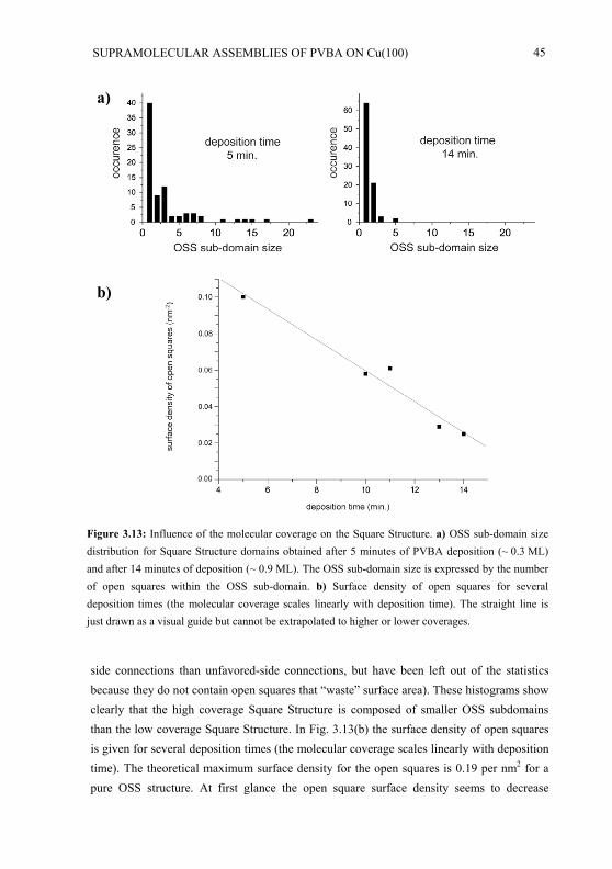
SUPRAMOLECULAR ASSEMBLIES OF PVBA ON Cu(100) 45
a)
b)
Figure 3.13: Influence of the molecular coverage on the Square Structure. a) OSS sub-domain size distribution for Square Structure domains obtained after 5 minutes of PVBA deposition (~ 0.3 ML)and after 14 minutes of deposition (~ 0.9 ML). The OSS sub-domain size is expressed by the numberof open squares within the OSS sub-domain. b) Surface density of open squares for severaldeposition times (the molecular coverage scales linearly with deposition time). The straight line is just drawn as a visual guide but cannot be extrapolated to higher or lower coverages.
side connections than unfavored-side connections, but have been left out of the statistics because they do not contain open squares that “waste” surface area). These histograms show clearly that the high coverage Square Structure is composed of smaller OSS subdomainsthan the low coverage Square Structure. In Fig. 3.13(b) the surface density of open squares is given for several deposition times (the molecular coverage scales linearly with deposition time). The theoretical maximum surface density for the open squares is 0.19 per nm2 for apure OSS structure. At first glance the open square surface density seems to decrease
46
linearly with molecular coverage, even at lower coverages. The linear decrease cannot be caused by compression of the domains due to space limitations because at low coverages the major part of the substrate is empty. Moreover, the molecular surface density within a domain increases just slowly with the overall molecular coverage: 0.74 nm-2 for a theoretical pure OSS structure and ~0.78 nm-2 for a Square Structure domain after 14 minutes of deposition (which is only a 5% increase in density against an increase of overall molecular coverage by several hundreds of percents). The molecular coverage on the substrate influences the rate with which molecules arrive at the domain edges during condensation of the domains after post-annealing. This rate presumably determines the percentage of unfavored-side bonding and hence the size of the OSS subdomains and the packing density of the Square Structure. Furthermore space limitations might come into play at high coverages. It should be noted here that even in parts of the Square Structure that do not contain any open squares, the favored-side to unfavored-side bonding ratio is not in equilibrium but stays around 3:2.
3.2.2 High coverage: Butterfly Structure
At saturation coverage (deposition of 1.0 ML or more and subsequent post-annealing to 400 K for 5 minutes) the structure shown in the STM image of Fig. 3.14(a) is formed. The dimers and open squares that characterize the Square Structure are not present anymore. The two homo-chiral phases have vanished and a single phase has developed, which has a long range ordering throughout the whole domain, in contrast to the Square Structure. In the structure of Fig. 3.14(a), each molecule points with one end to a spot where four molecules come together, creating a butterfly-shaped ordering. This structure will therefore be referred to as the Butterfly Structure. Coexistence of Square and Butterfly domains, or structures that are a local mixture of these two structures, have been observed for coverages between 0.9 and 1.0 ML. Molecules in excess of 1 ML desorb during post-annealing, resulting finally in the Butterfly Structure.
A detailed analysis of the data reveals that the symmetry axes of each “butterfly” in the Butterfly Structure follow the [001] and [010] substrate directions. For each butterfly the four next-nearest butterflies are rotated by 90°. The molecules in the Butterfly Structure are lying flat on the substrate, and are usually imaged by STM in the same way as for the Square Structure. XPS measurements show that also for the Butterfly Structure the carboxylic acid group of the PVBA molecules is deprotonated. The inter-molecular bonding however is different for both structures.
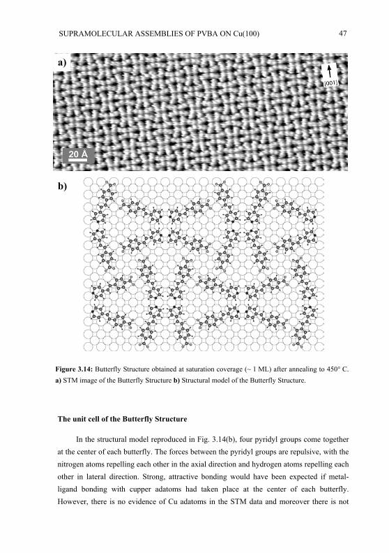
SUPRAMOLECULAR ASSEMBLIES OF PVBA ON Cu(100) 47
a)
b)
Figure 3.14: Butterfly Structure obtained at saturation coverage (~ 1 ML) after annealing to 450° C.a) STM image of the Butterfly Structure b) Structural model of the Butterfly Structure.
The unit cell of the Butterfly Structure
In the structural model reproduced in Fig. 3.14(b), four pyridyl groups come together at the center of each butterfly. The forces between the pyridyl groups are repulsive, with thenitrogen atoms repelling each other in the axial direction and hydrogen atoms repelling each other in lateral direction. Strong, attractive bonding would have been expected if metal-ligand bonding with cupper adatoms had taken place at the center of each butterfly. However, there is no evidence of Cu adatoms in the STM data and moreover there is not
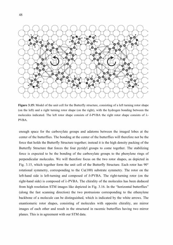
48
Figure 3.15: Model of the unit cell for the Butterfly structure, consisting of a left turning rotor shape (on the left) and a right turning rotor shape (on the right), with the hydrogen bonding between the molecules indicated. The left rotor shape consists of -PVBA the right rotor shape consists of -PVBA.
enough space for the carboxylate groups and adatoms between the imaged lobes at the center of the butterflies. The bonding at the center of the butterflies will therefore not be the force that holds the Butterfly Structure together; instead it is the high density packing of the Butterfly Structure that forces the four pyridyl groups to come together. The stabilizing force is expected to be the bonding of the carboxylate groups to the phenylene rings of perpendicular molecules. We will therefore focus on the two rotor shapes, as depicted in Fig. 3.15, which together form the unit cell of the Butterfly Structure. Each rotor has 90°rotational symmetry, corresponding to the Cu(100) substrate symmetry. The rotor on the left-hand side is left-turning and composed of -PVBA. The right-turning rotor (on the right-hand side) is composed of -PVBA. The chirality of the molecules has been deducedfrom high resolution STM images like depicted in Fig. 3.16. In the “horizontal butterflies”(along the fast scanning direction) the two protrusions corresponding to the ethenylene backbone of a molecule can be distinguished, which is indicated by the white arrows. Theenantiomeric rotor shapes, consisting of molecules with opposite chirality, are mirrorimages of each other and result in the structural in racemic butterflies having two mirrorplanes. This is in agreement with our STM data.
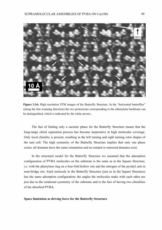
SUPRAMOLECULAR ASSEMBLIES OF PVBA ON Cu(100) 49
Figure 3.16: High resolution STM images of the Butterfly Structure. In the “horizontal butterflies”(along the fast scanning direction) the two protrusions corresponding to the ethenylene backbone canbe distinguished, which is indicated by the white arrows.
The fact of finding only a racemic phase for the Butterfly Structure means that thelong-range chiral separation process has become inoperative at high molecular coverage. Only local chirality is present, resulting in the left turning and right turning rotor shapes ofthe unit cell. The high symmetry of the Butterfly Structure implies that only one phase exists; all domains have the same orientation and no rotated or mirrored domains exist.
In the structural model for the Butterfly Structure we assumed that the adsorptionconfiguration of PVBA molecules on the substrate is the same as in the Square Structure, i.e. with the phenylene ring on a four-fold hollow site and the nitrogen of the pyridyl unit in near-bridge site. Each molecule in the Butterfly Structure (just as in the Square Structure)has the same adsorption configuration; the angles the molecules make with each other are just due to the rotational symmetry of the substrate and to the fact of having two chiralitiesof the absorbed PVBA.
Space limitation as driving force for the Butterfly Structure
50
The only difference in sample preparation leading to either the Butterfly Structure or the Square Structure, is the molecular coverage on the substrate. The Butterfly Structure can even be created by a second deposition of PVBA molecules (and subsequent annealing) on a substrate that already contains the Square Structure. As discussed before in this chapter, in both structures the molecules are deprotonated and lying flat on the substrate and no Cu adatoms are incorporated in either of the structures. The fact of finding two different structures is therefore attributed to the limited space per molecule on the substrate surface at high molecular coverages. This is in agreement with the fact that our STM data show that butterfly domains are always confined between stepedges or mixed structure domains and do not terminate in empty substrate. In fact, no empty substrate can be found at all when the Butterfly Structure is present on the substrate. The Butterfly Structure shows a denser molecular packing than the Square Structure, notably 0.83 molecules per nm2 for the Butterfly Structure and ~0.78 molecules per nm2 for a high coverage (0.9 ML) Square Structure. The sudden transition from Square Structure to Butterfly Structure with the increase of molecular coverage (0.9 ML vs. 1.0 ML) is in agreement with the relatively small difference in area taken per molecule for both structures. This difference only amounts to 6%.
Comparison of the propeller shaped crosses of the Square Structure (see Fig. 3.10(b)) and the rotor shapes of the Butterfly Structure (see Fig. 3.15), shows that the tail-to-side bonding for the Square Structure takes place more towards the pyridyl ring of a molecule whereas for the Butterfly Structure it takes place more towards the phenylene ring. The hydrogen bond lengths for the Butterfly Structure are between 2.7 and 3.6 Å (H···O distance), whereas for favored-side bonding in the Square Structure 3 of the 4 bond lengths are around 2.0 Å. The bonding configuration of the Butterfly Structure apparently leads to weaker hydrogen bonding, but enables a closer packing of the molecules. In short it can be stated that the Square Structure is more efficient if there are no space limitations, whereas Butterfly Structure domains are only found if there is not enough space on the substrate to form only the Square Structure.
3.3 Conclusion
The structures that are formed by PVBA deposited on a Cu(110) substrate show a strong dependence on the molecular coverage. Two distinct phases are found: the Square Structure for low molecular coverage and the Butterfly Structure for high molecular coverage. The transition from Square Structure to Butterfly Structure takes place around
SUPRAMOLECULAR ASSEMBLIES OF PVBA ON Cu(100) 51
0.9 ML molecular coverage. In both structures the molecules are lying flat on the substrate and the carboxylic acid group is deprotonated.
The Square Structure consists of dimers that are internally bound by hydrogen bonding between the pyridyl groups of both molecules and by possible substrate-mediated attraction. Two different, enantiomerically pure structures are found, named L domains and R domains, that are mirror-imaged in the [001] direction and consist of respectively -PVBA and -PVBA. This indicates that in this system chiral separation of the PVBA 2D
enantiomers takes place over mesoscopic distances to form enantiomerically pure domains. The carboxylate endgroups of each dimer bind to the sides of molecules of perpendicularly oriented dimers. The carboxylate groups can bind to both sides of a molecule, but can make stronger hydrogen bonding on one specific side, which depends on the chirality of the domain (and hence the chirality of the molecules). For L domains bonding to the left side is favored and for R domains bonding to the right side is favored. STM data have shown that favored-side and unfavored-side bonding take place in a typically 3:1 ratio for coverages around 0.5 ML. Square Structure domains are built of small Open Square Structure subdomains in which, away from the edges, only favored-side bonding occurs. The observed ordering of the Square Structure is assumed to be a compromise between strongest bonding and packing density (which is higher when both favored-side and unfavored-side bonding take place). With increasing molecular coverage, the packing density of the Square Structure increases, the size of the OSS subdomains decreases and the bonding ratio (favored-side : unfavored-side) decreases. The rate with which molecules arrive at the domain edges during condensation of the domains possibly determines the fraction of unfavored-side bonding.
The Butterfly Structure domains are racemic and have a long range ordering throughout the whole domain, in contrast to the Square Structure. The unit cell of the Butterfly Structure consists of two rotor shaped arrangements in which hydrogen bonding takes place between the carboxylate groups and sides of molecules. One rotor shape consists of -PVBA and the other consists of -PVBA. Hence chiral separation is suppressed at high molecular coverage. In the Butterfly Structure four pyridyl groups come together at the center of each ‘butterfly’ unit. Repulsive forces are present between the pyridyl groups, but the packing of the Butterfly Structure pushes the four pyridyl groups together. The Butterfly Structure shows a 6% closer packing than the Square Structure and can only be found when there is no empty space left on the sample. The transition from Square Structure to Butterfly Structure is driven by space limitations at high molecular coverages.

52
Chapter 4
Carbon nanotube growth and
functionalization
Carbon nanotubes are very interesting candidates for a multitude of applications, dueto their exceptional mechanical and electrical properties. They can be used as single-molecule transistors [8] [9] and they are considered for connecting molecular devices and asinterconnects on chips [10]. Other applications of nanotubes are the use of these moleculesas sensors [77], as emitters for light sources based on field emission [78] [79], and the firstworking flat panel display based on carbon nanotube field emitters has been reported [80]. Based on their mechanical properties, carbon nanotubes could replace conventional carbon fibers for making materials that are both strong and light. On a smaller scale their mechanical properties have been exploited successfully by using carbon nanotubes as AFMimaging tips [81] and for scanning probe lithography [82].
One of the keys to a successful use of nanotubes in molecular electronics and otherapplications is the controlled growth and positioning of nanotubes. Ideally, one should beable to place one nanotube or an assembly of nanotubes with well-defined properties on precise locations on a support. In the first part of this chapter a technique is described which allows to grow patterns of vertically aligned nanotubes with a very narrow diameterdistribution and nanotube lengths that can be steered by the growth conditions. Thenanotubes can be grown at large scale without encapsulated catalyst particles or attached amorphous carbon.
For integration of the nanotubes within real devices, good electrical and/or mechanicalcontacts have to be made either to other materials or to other nanotubes. In the second part
53
54
of this chapter metal coatings deposited on nanotubes are studied and a method for cross-linking carbon nanotubes is presented. Cross-linking can be important for the creation of nanotube networks for microelectronics. Moreover, if the cross-links between the nanotubes establish a stable connection, it should also be possible to create very strong polymercompound materials. Up to now the mechanical strength of nanotube-polymer composites is much lower than that of pure nanotubes [83] because the nanotubes in compound materialsslip out of the polymer matrix when large forces are applied. This is due to the saturatedbonds on the surface of the nanotubes and the resulting weak bonding to their environment.Nanotube networks made by cross-linking can help herein.
4.1 Experimental
In this section first the experimental methods are described that have been used forgrowing carbon nanotubes. Catalyst particles were deposited on a silicon substrate using the micro contact printing ( CP) technique. These catalyst particles are used for growing carbon nanotubes using Chemical Vapor Deposition (CVD). In the following ScanningElectron Microscopy (SEM) and Transmission Electron Microscopy (TEM) are discussed shortly, which have been used for observing and analyzing the nanotubes and the metalcoatings deposited on nanotubes. Finally the theory and set-up for Field Emissionmeasurements will be described.
b)a)
Figure 4.1: Single-walled carbon nanotube a) Illustration of a single-walled carbon nanotubeshowing the tube end being closed by half a fullerene molecule. b) Honeycomb structure of agraphene sheet with three examples of lattice vectors along which the sheet can be folded to form a nanotube. The structural parameters give the direction and length of the lattice vectors expressed in units of the basis vectors a1 and a2. This image is taken from [86].
CARBON NANOTUBE GROWTH AND FUNCTIONALIZATION 55
4.1.1. Carbon nanotubes
Carbon nanotubes are unique single molecules that emerged from the fullerene familyhigh resolution transmission electron microscopy in 1991
by Iijima [7]. Single-walled carbon nanotubes (SW-CNT) are carbon macromoleculesconsi
[84], and have been discovered by
sting of graphene sheets rolled into a cylinder with a typical diameter in the order of 1.4 nm and lengths up to hundreds of micrometers. The ends of the cylinder can be capped with half of a fullerene molecule (see Fig. 4.1(a)). Nanotubes are composed entirely of sp²bonds, similar to graphite, but with an orbital rehybridization caused by the curved nanotube walls. This bonding is stronger than the sp3 bonds found in diamond, and provides the nanotubes with their unique strength. They have a Young’s modulus of typically 1.3 TPa
a) b) c) d)
Figure 4.2: Schematic structures of single-walled carbon nanotubes and how they determine the electronic properties of the nanotubes. a) A (10,10) arm-chair nanotube. Bottom panel: the hexagonrepresents the first Brillouin zone of a graphene sheet in reciprocal space. The vertical lines representthe electronic states of the nanotube. The center-line crosses two corners of the hexagon, resulting ina metallic nanotube. b) A (12, 0) zigzag nanotube. The electronic states cross the hexagon corners,but a small band gap develops due to the curvature of the nanotube. c) The (14, 0) zigzag tube is semiconducting because the states on the vertical lines miss the corner points of the hexagon. d) Alsothe (7, 16) tube is semiconducting. These images are taken from [86].
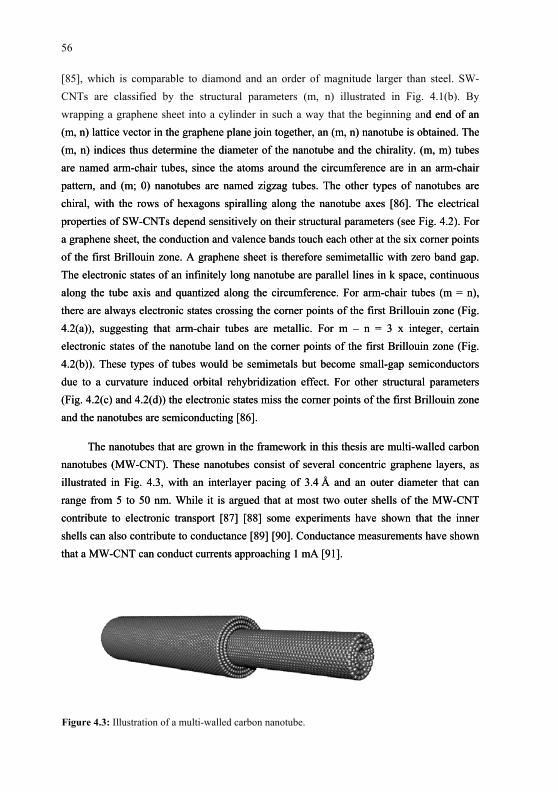
56
[85], which is comparable to diamond and an order of magnitude larger than steel. SW-CNTs are classified by the structural parameters (m, n) illustrated in Fig. 4.1(b). By wrapping a graphene sheet into a cylinder in such a way that the beginning and end of an(m, n) lattice vector in the graphene plane join together, an (m, n) nanotube is obtained. The(m, n) indices thus determine the diameter of the nanotube and the chirality. (m, m) tubes are named arm-chair tubes, since the atoms around the circumference are in an arm-chair pattern, and (m; 0) nanotubes are named zigzag tubes. The other types of nanotubes are chiral, with the rows of hexagons spiralling along the nanotube axes [86]. The electrical properties of SW-CNTs depend sensitively on their structural parameters (see Fig. 4.2). For a graphene sheet, the conduction and valence bands touch each other at the six corner pointsof the first Brillouin zone. A graphene sheet is therefore semimetallic with zero band gap. The electronic states of an infinitely long nanotube are parallel lines in k space, continuousalong the tube axis and quantized along the circumference. For arm-chair tubes (m = n), there are always electronic states crossing the corner points of the first Brillouin zone (Fig. 4.2(a)), suggesting that arm-chair tubes are metallic. For m – n = 3 x integer, certain electronic states of the nanotube land on the corner points of the first Brillouin zone (Fig. 4.2(b)). These types of tubes would be semimetals but become small-gap semiconductorsdue to a curvature induced orbital rehybridization effect. For other structural parameters(Fig. 4.2(c) and 4.2(d)) the electronic states miss the corner points of the first Brillouin zone and the nanotubes are semiconducting [86].
The nanotubes that are grown in the fram
d end of an(m, n) lattice vector in the graphene plane join together, an (m, n) nanotube is obtained. The(m, n) indices thus determine the diameter of the nanotube and the chirality. (m, m) tubes are named arm-chair tubes, since the atoms around the circumference are in an arm-chair pattern, and (m; 0) nanotubes are named zigzag tubes. The other types of nanotubes are chiral, with the rows of hexagons spiralling along the nanotube axes [86]. The electrical properties of SW-CNTs depend sensitively on their structural parameters (see Fig. 4.2). For a graphene sheet, the conduction and valence bands touch each other at the six corner pointsof the first Brillouin zone. A graphene sheet is therefore semimetallic with zero band gap. The electronic states of an infinitely long nanotube are parallel lines in k space, continuousalong the tube axis and quantized along the circumference. For arm-chair tubes (m = n), there are always electronic states crossing the corner points of the first Brillouin zone (Fig. 4.2(a)), suggesting that arm-chair tubes are metallic. For m – n = 3 x integer, certain electronic states of the nanotube land on the corner points of the first Brillouin zone (Fig. 4.2(b)). These types of tubes would be semimetals but become small-gap semiconductorsdue to a curvature induced orbital rehybridization effect. For other structural parameters(Fig. 4.2(c) and 4.2(d)) the electronic states miss the corner points of the first Brillouin zone and the nanotubes are semiconducting [86].
The nanotubes that are grown in the framework in this thesis are multi-walled carbonnanotubes (MW-CNT). These nanotubes consist of several concentric graphene layers, as illustr
ework in this thesis are multi-walled carbonnanotubes (MW-CNT). These nanotubes consist of several concentric graphene layers, as illustrated in Fig. 4.3, with an interlayer pacing of 3.4 Å and an outer diameter that canrange from 5 to 50 nm. While it is argued that at most two outer shells of the MW-CNT contribute to electronic transport [87] [88] some experiments have shown that the innershells can also contribute to conductance [89] [90]. Conductance measurements have shown that a MW-CNT can conduct currents approaching 1 mA [91].
ated in Fig. 4.3, with an interlayer pacing of 3.4 Å and an outer diameter that canrange from 5 to 50 nm. While it is argued that at most two outer shells of the MW-CNT contribute to electronic transport [87] [88] some experiments have shown that the innershells can also contribute to conductance [89] [90]. Conductance measurements have shown that a MW-CNT can conduct currents approaching 1 mA [91].
Figure 4.3: Illustration of a multi-walled carbon nanotube.
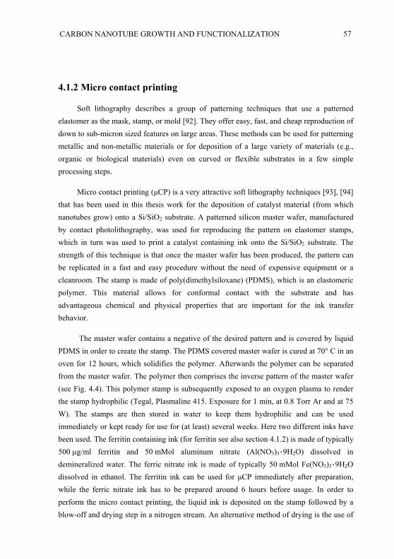
CARBON NANOTUBE GROWTH AND FUNCTIONALIZATION 57
4.1.2 Micro contact printing
Soft lithography describes a group of patterning techniques that use a patterned elastomer as the mask, stamp, or mold [92]. They offer easy, fast, and cheap reproduction of down to sub-micron sized features on large areas. These methods can be used for patterning metallic and non-metallic materials or for deposition of a large variety of materials (e.g., organic or biological materials) even on curved or flexible substrates in a few simple processing steps.
Micro contact printing (µCP) is a very attractive soft lithography techniques [93], [94] that has been used in this thesis work for the deposition of catalyst material (from which nanotubes grow) onto a Si/SiO2 substrate. A patterned silicon master wafer, manufactured by contact photolithography, was used for reproducing the pattern on elastomer stamps, which in turn was used to print a catalyst containing ink onto the Si/SiO2 substrate. The strength of this technique is that once the master wafer has been produced, the pattern can be replicated in a fast and easy procedure without the need of expensive equipment or a cleanroom. The stamp is made of poly(dimethylsiloxane) (PDMS), which is an elastomeric polymer. This material allows for conformal contact with the substrate and has advantageous chemical and physical properties that are important for the ink transfer behavior.
The master wafer contains a negative of the desired pattern and is covered by liquid PDMS in order to create the stamp. The PDMS covered master wafer is cured at 70° C in an oven for 12 hours, which solidifies the polymer. Afterwards the polymer can be separated from the master wafer. The polymer then comprises the inverse pattern of the master wafer (see Fig. 4.4). This polymer stamp is subsequently exposed to an oxygen plasma to render the stamp hydrophilic (Tegal, Plasmaline 415. Exposure for 1 min, at 0.8 Torr Ar and at 75 W). The stamps are then stored in water to keep them hydrophilic and can be used immediately or kept ready for use for (at least) several weeks. Here two different inks have been used. The ferritin containing ink (for ferritin see also section 4.1.2) is made of typically 500 g/ml ferritin and 50 mMol aluminum nitrate (Al(NO3)3·9H2O) dissolved in demineralized water. The ferric nitrate ink is made of typically 50 mMol Fe(NO3)3·9H2Odissolved in ethanol. The ferritin ink can be used for µCP immediately after preparation, while the ferric nitrate ink has to be prepared around 6 hours before usage. In order to perform the micro contact printing, the liquid ink is deposited on the stamp followed by a blow-off and drying step in a nitrogen stream. An alternative method of drying is the use of
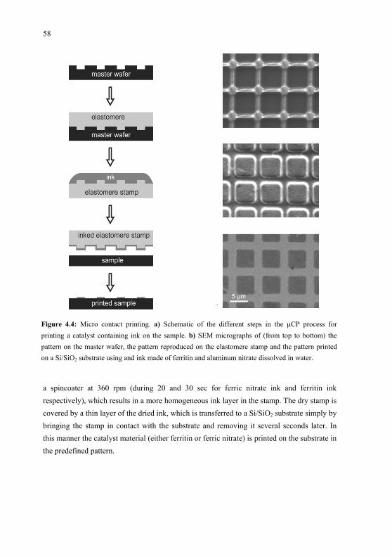
58
bFigure 4.4: Micro contact printing. a) Schematic of the different steps in the CP process forprinting a catalyst containing ink on the sample. b) SEM micrographs of (from top to bottom) the pattern on the master wafer, the pattern reproduced on the elastomere stamp and the pattern printed on a Si/SiO2 substrate using and ink made of ferritin and aluminum nitrate dissolved in water.
a spincoater at 360 rpm (during 20 and 30 sec for ferric nitrate ink and ferritin inkrespectively), which results in a more homogeneous ink layer in the stamp. The dry stamp iscovered by a thin layer of the dried ink, which is transferred to a Si/SiO2 substrate simply by bringing the stamp in contact with the substrate and removing it several seconds later. In this manner the catalyst material (either ferritin or ferric nitrate) is printed on the substrate in the predefined pattern.
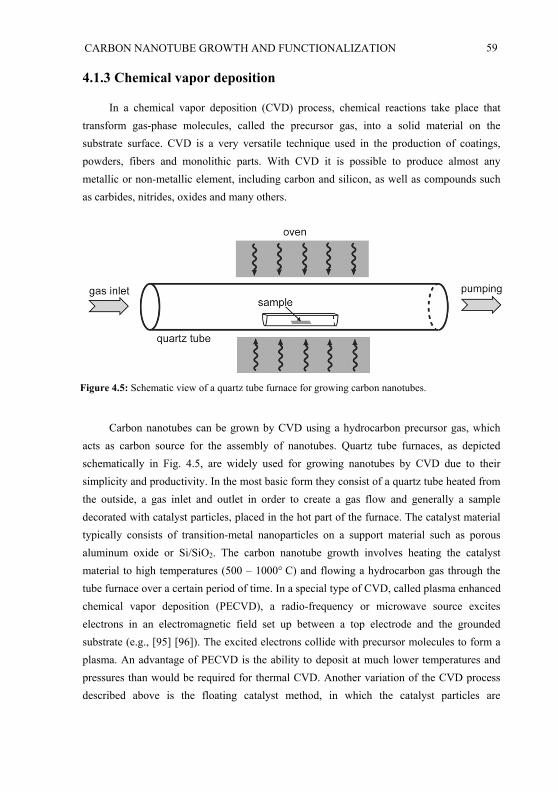
CARBON NANOTUBE GROWTH AND FUNCTIONALIZATION 59
4.1.3 Chemical vapor deposition
In a chemical vapor deposition (CVD) process, chemical reactions take place that transform gas-phase molecules, called the precursor gas, into a solid material on the substrate surface. CVD is a very versatile technique used in the production of coatings,powders, fibers and monolithic parts. With CVD it is possible to produce almost anymetallic or non-metallic element, including carbon and silicon, as well as compounds suchas carbides, nitrides, oxides and many others.
Figure 4.5: Schematic view of a quartz tube furnace for growing carbon nanotubes.
Carbon nanotubes can be grown by CVD using a hydrocarbon precursor gas, which acts as carbon source for the assembly of nanotubes. Quartz tube furnaces, as depictedschematically in Fig. 4.5, are widely used for growing nanotubes by CVD due to their simplicity and productivity. In the most basic form they consist of a quartz tube heated from the outside, a gas inlet and outlet in order to create a gas flow and generally a sampledecorated with catalyst particles, placed in the hot part of the furnace. The catalyst materialtypically consists of transition-metal nanoparticles on a support material such as porous aluminum oxide or Si/SiO2. The carbon nanotube growth involves heating the catalyst material to high temperatures (500 – 1000° C) and flowing a hydrocarbon gas through the tube furnace over a certain period of time. In a special type of CVD, called plasma enhancedchemical vapor deposition (PECVD), a radio-frequency or microwave source exciteselectrons in an electromagnetic field set up between a top electrode and the grounded substrate (e.g., [95] [96]). The excited electrons collide with precursor molecules to form a plasma. An advantage of PECVD is the ability to deposit at much lower temperatures and pressures than would be required for thermal CVD. Another variation of the CVD process described above is the floating catalyst method, in which the catalyst particles are
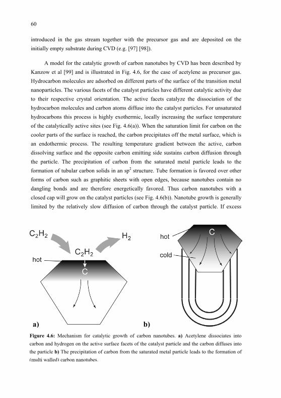
60
introduced in the gas stream together with the precursor gas and are deposited on the initially empty substrate during CVD (e.g. [97] [98]).
A model for the catalytic growth of carbon nanotubes by CVD has been described by Kanzow et al [99] and is illustrated in Fig. 4.6, for the case of acetylene as precursor gas. Hydrocarbon molecules are adsorbed on different parts of the surface of the transition metalnanoparticles. The various facets of the catalyst particles have different catalytic activity dueto their respective crystal orientation. The active facets catalyze the dissociation of thehydrocarbon molecules and carbon atoms diffuse into the catalyst particles. For unsaturated hydrocarbons this process is highly exothermic, locally increasing the surface temperatureof the catalytically active sites (see Fig. 4.6(a)). When the saturation limit for carbon on the cooler parts of the surface is reached, the carbon precipitates off the metal surface, which is an endothermic process. The resulting temperature gradient between the active, carbon dissolving surface and the opposite carbon emitting side sustains carbon diffusion through the particle. The precipitation of carbon from the saturated metal particle leads to the formation of tubular carbon solids in an sp2 structure. Tube formation is favored over other forms of carbon such as graphitic sheets with open edges, because nanotubes contain no dangling bonds and are therefore energetically favored. Thus carbon nanotubes with aclosed cap will grow on the catalyst particles (see Fig. 4.6(b)). Nanotube growth is generallylimited by the relatively slow diffusion of carbon through the catalyst particle. If excess
a) b)Figure 4.6: Mechanism for catalytic growth of carbon nanotubes. a) Acetylene dissociates intocarbon and hydrogen on the active surface facets of the catalyst particle and the carbon diffuses intothe particle b) The precipitation of carbon from the saturated metal particle leads to the formation of(multi walled) carbon nanotubes.
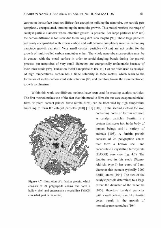
CARBON NANOTUBE GROWTH AND FUNCTIONALIZATION 61
carbon on the surface does not diffuse fast enough to build up the nanotube, the particle getscompletely encapsulated, terminating the nanotube growth. This model restricts the range of catalyst particle diameter where effective growth is possible. For large particles (>25 nm)the carbon diffusion is too slow due to the long diffusion lengths [99]. These large particles get easily encapsulated with excess carbon and will become completely inactive before any nanotube growth can start. Very small catalyst particles (<3 nm) are not useful for the growth of multi-walled carbon nanotubes either. The whole nanotube cross-section must be in contact with the metal surface in order to avoid dangling bonds during the growth process, but nanotubes of very small diameters are energetically unfavorable because of their inner strain [99]. Transition-metal nanoparticles (Fe, Ni, Co) are often used as catalyst. At high temperatures, carbon has a finite solubility in these metals, which leads to theformation of metal–carbon solid state solutions [86] and therefore favors the aforementionedgrowth mechanism.
Within this work two different methods have been used for creating catalyst particles. The first method makes use of the fact that thin metallic films (in our case evaporated nickel films or micro contact printed ferric nitrate films) can be fractioned by high temperatureannealing to form the catalyst particles [100] [101] [102]. In the second method the iron
containing cores of ferritin are usedas catalyst particles. Ferritin is a protein that stores iron in the body of human beings and a variety of animals [103]. A ferritin protein consists of 24 polypeptide chains that form a hollow shell andencapsulate a crystalline ferrihydrate(FeOOH) core (see Fig. 4.7). The ferritin used in this study (Sigma-Aldrich, type I) has cores of 5 nmdiameter that contain typically 3000 Fe(III) atoms [104]. The size of the catalyst particle determines to a largeextent the diameter of the nanotube [105], therefore catalyst particles with a well defined size, like ferritincores, result in the growth of monodisperse nanotubes [104].
Figure 4.7: Illustration of a ferritin protein, which consists of 24 polypeptide chains that form ahollow shell and encapsulate a crystalline FeOOHcore (dark part in the center).

62
We used thermal CVD at temperatures between 660 and 800° C in a quartz tube furnace. An acetylene flow at 20 mbar is used as precursor gas and is pumped away at the gas outlet using a primary pump. A quartz boat (a hollow, closed cylinder cut along the cylinder axis) is used to transfer the samples into the middle of the furnace which is already at the required temperature. The sample is kept there for 2 minutes in which time the sample obtains the required temperature and fractioning of the thin metallic catalyst layer can take place. In the meantime the furnace is pumped to typically 0.01 mbar. Subsequently the acetylene flow is started and continued for 5 minutes. After the CVD growth the sample is cooled down in a nitrogen atmosphere. It turned out that the CP samples, both with ferritin and with ferric nitrate, in many cases need to be exposed to oxygen before CVD start, in order to have good nanotube growth. The oxygen exposure and the influence of the CVD parameters on the nanotube growth are discussed in section 4.2.2.
4.1.4 Electron Microscopy
The transmission electron microscope (TEM) is a derivative of the light microscope. It makes use of the fact that the wavelength of electrons is shorter than visible light. Hence higher resolutions are possible and even atomic resolution can be achieved. The high-energy electrons have wavelengths that are an order of magnitude smaller than the interplanar distance in most crystals, which opens the possibility to use a TEM also for crystallographic microanalysis by studying diffraction patterns. A TEM uses electron lenses, which are the electronic equivalent of convex optical lenses, to focus the electrons that are transmitted through the specimen and create a magnified image on a fluorescent screen, a photographic film or a CCD camera. A schematic of a TEM is depicted in Fig. 4.8(a) in the most general form. The condenser lenses and the condenser aperture determine the convergence of the beam at the specimen and determine the diameter and intensity of the illuminated area of the specimen [106]. The electrons that are transmitted through the specimen are formed into an initial image of the specimen by the objective lens. In the back focal plane of the objective lens a diffraction pattern is formed. The objective aperture can be inserted here, which influences the contrast of the final image and also the depth of field at the specimen and the depth of focus at the screen. The intermediate lens can be focused on either the initial image formed by the objective lens, or on the diffraction pattern formed in the back focal plane of the objective lens. This determines whether the viewing screen of the microscope shows an image or a diffraction pattern. Magnification in the electron microscope can be varied from hundred to several hundred thousand fold. This is done by varying the strength of the projector lens (or lenses).
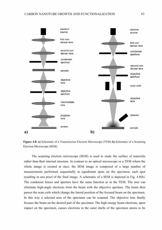
CARBON NANOTUBE GROWTH AND FUNCTIONALIZATION 63
a) b)
Figure 4.8: a) Schematic of a Transmission Electron Microscope (TEM) b) Schematic of a ScanningElectron Microscope (SEM)
The scanning electron microscope (SEM) is used to study the surface of materialsrather than their internal structure. In contrast to an optical microscope or a TEM where the whole image is created at once, the SEM image is composed of a large number of measurements performed sequentially at equidistant spots on the specimen; each spot resulting in one pixel of the final image. A schematic of a SEM is depicted in Fig. 4.8(b).The condenser lenses and aperture have the same function as in the TEM. The user can eliminate high-angle electrons from the beam with the objective aperture. The beam then passes the scan coils which change the lateral position of the focused beam on the specimen.In this way a selected area of the specimen can be scanned. The objective lens finally focuses the beam on the desired part of the specimen. The high energy beam electrons, upon impact on the specimen, causes electrons in the outer shells of the specimen atoms to be
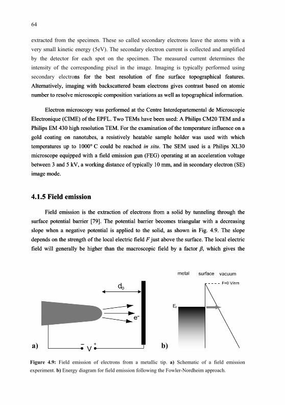
64
extracted from the specimen. These so called secondary electrons leave the atoms with a very small kinetic energy (5eV). The secondary electron current is collected and amplified by the detector for each spot on the specimen. The measured current determines the intensity of the corresponding pixel in the image. Imaging is typically performed using secondary electrons for the best resolution of fine surface topographical features.Alternatively, imaging with backscattered beam electrons gives contrast based on atomicnumber to resolve microscopic composition variations as well as topographical information.
ns for the best resolution of fine surface topographical features.Alternatively, imaging with backscattered beam electrons gives contrast based on atomicnumber to resolve microscopic composition variations as well as topographical information.
Electron microscopy was performed at the Centre Interdepartemental de Microscopie Electronique (CIME) of the EPFL. Two TEMs have been used: A Philips CM20 TEM and a Philips EM 430 high resolution TEM. For the examination of the temperature influence on a gold coating on nanotubes, a resistively heatable sample holder was used with which temperatures up to 1000° C could be reached in situ. The SEM used is a Philips XL30 microscope equipped with a field emission gun (FEG) operating at an acceleration voltage between 3 and 5 kV, a working distance of typically 10 mm, and in secondary electron (SE) image mode.
Electron microscopy was performed at the Centre Interdepartemental de Microscopie Electronique (CIME) of the EPFL. Two TEMs have been used: A Philips CM20 TEM and a Philips EM 430 high resolution TEM. For the examination of the temperature influence on a gold coating on nanotubes, a resistively heatable sample holder was used with which temperatures up to 1000° C could be reached in situ. The SEM used is a Philips XL30 microscope equipped with a field emission gun (FEG) operating at an acceleration voltage between 3 and 5 kV, a working distance of typically 10 mm, and in secondary electron (SE) image mode.
4.1.5 Field emission 4.1.5 Field emission
Field emission is the extraction of electrons from a solid by tunneling through the surface potential barrier [79]. The potential barrier becomes triangular with a decreasingslope when a negative potential is applied to the solid, as shown in Fig. 4.9. The slope depends on the strength of the local electric field F just above the surface. The local electric field will generally be higher than the macroscopic field by a factor , which gives the
Field emission is the extraction of electrons from a solid by tunneling through the surface potential barrier [79]. The potential barrier becomes triangular with a decreasingslope when a negative potential is applied to the solid, as shown in Fig. 4.9. The slope depends on the strength of the local electric field F just above the surface. The local electric field will generally be higher than the macroscopic field by a factor , which gives the
a) b)
Figure 4.9: Field emission of electrons from a metallic tip. a) Schematic of a field emissionexperiment. b) Energy diagram for field emission following the Fowler-Nordheim approach.
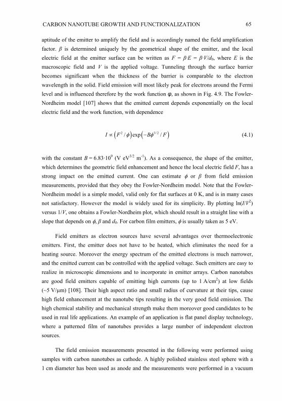
CARBON NANOTUBE GROWTH AND FUNCTIONALIZATION 65
aptitude of the emitter to amplify the field and is accordingly named the field amplificationfactor. is determined uniquely by the geometrical shape of the emitter, and the local electric field at the emitter surface can be written as F = ·E = ·V/d0, where E is themacroscopic field and V is the applied voltage. Tunneling through the surface barrier becomes significant when the thickness of the barrier is comparable to the electron wavelength in the solid. Field emission will most likely peak for electrons around the Fermilevel and is influenced therefore by the work function , as shown in Fig. 4.9. The Fowler-Nordheim model [107] shows that the emitted current depends exponentially on the local electric field and the work function, with dependence
2 3/ exp // 2I F B F (4.1)
with the constant B = 6.83·109 (V eV3/2 m-1). As a consequence, the shape of the emitter,which determines the geometric field enhancement and hence the local electric field F, has a strong impact on the emitted current. One can estimate or from field emissionmeasurements, provided that they obey the Fowler-Nordheim model. Note that the Fowler-Nordheim model is a simple model, valid only for flat surfaces at 0 K, and is in many cases not satisfactory. However the model is widely used for its simplicity. By plotting ln(I/V2)versus 1/V, one obtains a Fowler-Nordheim plot, which should result in a straight line with a slope that depends on , and d0. For carbon film emitters, is usually taken as 5 eV.
Field emitters as electron sources have several advantages over thermoelectronicemitters. First, the emitter does not have to be heated, which eliminates the need for a heating source. Moreover the energy spectrum of the emitted electrons is much narrower,and the emitted current can be controlled with the applied voltage. Such emitters are easy to realize in microscopic dimensions and to incorporate in emitter arrays. Carbon nanotubesare good field emitters capable of emitting high currents (up to 1 A/cm2) at low fields (~5 V/ m) [108]. Their high aspect ratio and small radius of curvature at their tips, cause high field enhancement at the nanotube tips resulting in the very good field emission. Thehigh chemical stability and mechanical strength make them moreover good candidates to be used in real life applications. An example of an application is flat panel display technology, where a patterned film of nanotubes provides a large number of independent electron sources.
The field emission measurements presented in the following were performed using samples with carbon nanotubes as cathode. A highly polished stainless steel sphere with a 1 cm diameter has been used as anode and the measurements were performed in a vacuum
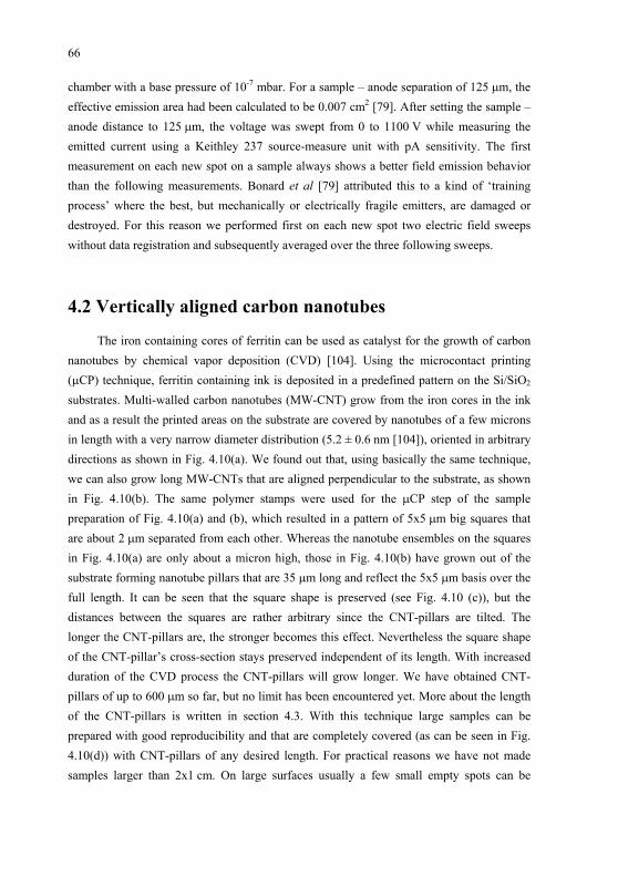
66
chamber with a base pressure of 10-7 mbar. For a sample – anode separation of 125 m, the effective emission area had been calculated to be 0.007 cm2 [79]. After setting the sample – anode distance to 125 m, the voltage was swept from 0 to 1100 V while measuring the emitted current using a Keithley 237 source-measure unit with pA sensitivity. The first measurement on each new spot on a sample always shows a better field emission behavior than the following measurements. Bonard et al [79] attributed this to a kind of ‘training process’ where the best, but mechanically or electrically fragile emitters, are damaged or destroyed. For this reason we performed first on each new spot two electric field sweeps without data registration and subsequently averaged over the three following sweeps.
4.2 Vertically aligned carbon nanotubes
The iron containing cores of ferritin can be used as catalyst for the growth of carbon nanotubes by chemical vapor deposition (CVD) [104]. Using the microcontact printing ( CP) technique, ferritin containing ink is deposited in a predefined pattern on the Si/SiO2
substrates. Multi-walled carbon nanotubes (MW-CNT) grow from the iron cores in the ink and as a result the printed areas on the substrate are covered by nanotubes of a few microns in length with a very narrow diameter distribution (5.2 ± 0.6 nm [104]), oriented in arbitrary directions as shown in Fig. 4.10(a). We found out that, using basically the same technique, we can also grow long MW-CNTs that are aligned perpendicular to the substrate, as shown in Fig. 4.10(b). The same polymer stamps were used for the CP step of the sample preparation of Fig. 4.10(a) and (b), which resulted in a pattern of 5x5 m big squares that are about 2 m separated from each other. Whereas the nanotube ensembles on the squares in Fig. 4.10(a) are only about a micron high, those in Fig. 4.10(b) have grown out of the substrate forming nanotube pillars that are 35 m long and reflect the 5x5 m basis over the full length. It can be seen that the square shape is preserved (see Fig. 4.10 (c)), but the distances between the squares are rather arbitrary since the CNT-pillars are tilted. The longer the CNT-pillars are, the stronger becomes this effect. Nevertheless the square shape of the CNT-pillar’s cross-section stays preserved independent of its length. With increased duration of the CVD process the CNT-pillars will grow longer. We have obtained CNT-pillars of up to 600 m so far, but no limit has been encountered yet. More about the length of the CNT-pillars is written in section 4.3. With this technique large samples can be prepared with good reproducibility and that are completely covered (as can be seen in Fig. 4.10(d)) with CNT-pillars of any desired length. For practical reasons we have not made samples larger than 2x1 cm. On large surfaces usually a few small empty spots can be
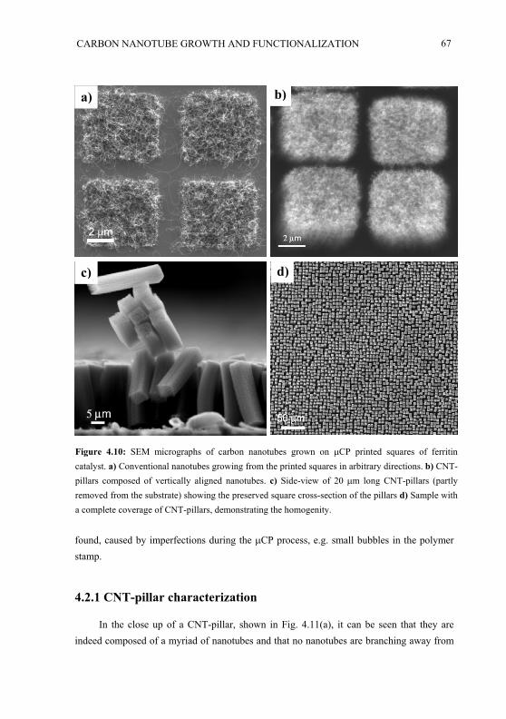
CARBON NANOTUBE GROWTH AND FUNCTIONALIZATION 67
b)a)
d)c)
Figure 4.10: SEM micrographs of carbon nanotubes grown on CP printed squares of ferritincatalyst. a) Conventional nanotubes growing from the printed squares in arbitrary directions. b) CNT-pillars composed of vertically aligned nanotubes. c) Side-view of 20 m long CNT-pillars (partly removed from the substrate) showing the preserved square cross-section of the pillars d) Sample witha complete coverage of CNT-pillars, demonstrating the homogenity.
found, caused by imperfections during the CP process, e.g. small bubbles in the polymerstamp.
4.2.1 CNT-pillar characterization
In the close up of a CNT-pillar, shown in Fig. 4.11(a), it can be seen that they areindeed composed of a myriad of nanotubes and that no nanotubes are branching away from
CP process, e.g. small bubbles in the polymer
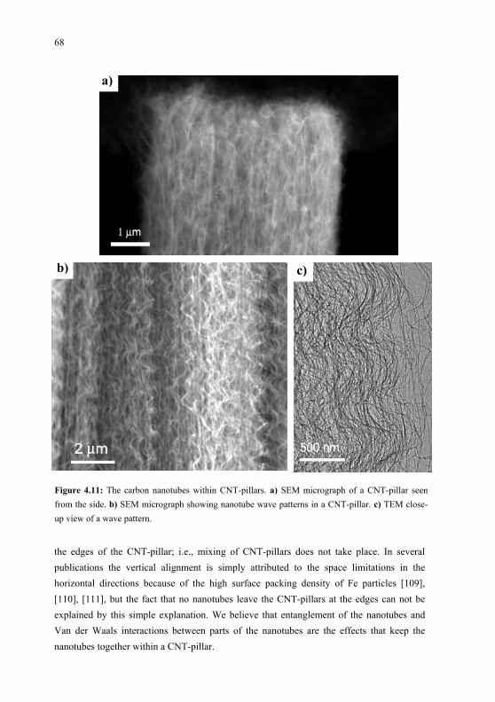
68
a)
b) c)
Figure 4.11: The carbon nanotubes within CNT-pillars. a) SEM micrograph of a CNT-pillar seenfrom the side. b) SEM micrograph showing nanotube wave patterns in a CNT-pillar. c) TEM close-up view of a wave pattern.
the edges of the CNT-pillar; i.e., mixing of CNT-pillars does not take place. In several publications the vertical alignment is simply attributed to the space limitations in the horizontal directions because of the high surface packing density of Fe particles [109], [110], [111], but the fact that no nanotubes leave the CNT-pillars at the edges can not beexplained by this simple explanation. We believe that entanglement of the nanotubes and Van der Waals interactions between parts of the nanotubes are the effects that keep the nanotubes together within a CNT-pillar.
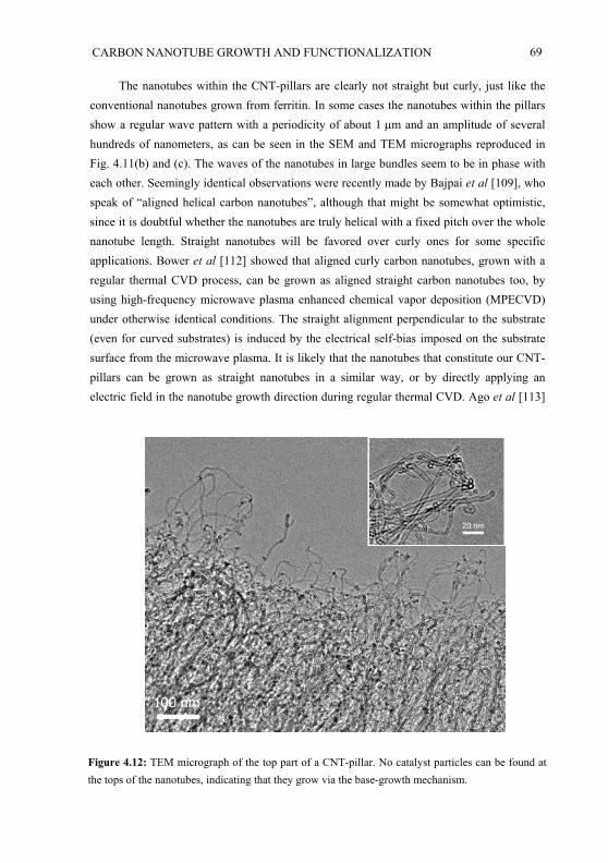
CARBON NANOTUBE GROWTH AND FUNCTIONALIZATION 69
tin. In some cases the nanotubes within the pillarsshow a regular wave pattern with a periodicity of about 1 m and an amplitude of several hundr
The nanotubes within the CNT-pillars are clearly not straight but curly, just like theconventional nanotubes grown from ferri
eds of nanometers, as can be seen in the SEM and TEM micrographs reproduced in Fig. 4.11(b) and (c). The waves of the nanotubes in large bundles seem to be in phase with each other. Seemingly identical observations were recently made by Bajpai et al [109], who speak of “aligned helical carbon nanotubes”, although that might be somewhat optimistic,since it is doubtful whether the nanotubes are truly helical with a fixed pitch over the whole nanotube length. Straight nanotubes will be favored over curly ones for some specificapplications. Bower et al [112] showed that aligned curly carbon nanotubes, grown with aregular thermal CVD process, can be grown as aligned straight carbon nanotubes too, by using high-frequency microwave plasma enhanced chemical vapor deposition (MPECVD)under otherwise identical conditions. The straight alignment perpendicular to the substrate(even for curved substrates) is induced by the electrical self-bias imposed on the substrate surface from the microwave plasma. It is likely that the nanotubes that constitute our CNT-pillars can be grown as straight nanotubes in a similar way, or by directly applying an electric field in the nanotube growth direction during regular thermal CVD. Ago et al [113]
Figure 4.12: TEM micrograph of the top part of a CNT-pillar. No catalyst particles can be found at the tops of the nanotubes, indicating that they grow via the base-growth mechanism.
70
proved moreover that pretreatment of catalyst particles can straighten vertically aligned nanotubes. However, the pretreatment to chose and its particular effect strongly depends on the catalyst and possibly also on the growth process itself.
In Fig. 4.12 TEM micrographs are presented of the top of a CNT-pillar that has been taken off the Si/SiO2 substrate and put on a TEM grid (the part of the CNT-pillar that is pointi
in this way do not contain any encapsulated catalyst particles, as can be verified in Fig. 4.12. Encap
. The attachment is strong enough to resist shaking and slight blowing with a nitrogen gun and weak enough to be
ng away from the substrate is regarded as the top). No catalyst particles are present at the ends of the nanotubes, which implies that the CNT-pillars are growing via a pure base-growth mechanism, where the catalyst particles stay at the substrate. This is in contrast to conventional nanotubes where about 10% of the nanotubes grow via the top-growth mechanism [114]. Thus the CNT-pillars grow purely from the bottom; in this way the square cross-section is preserved and the nanotubes can much more easily stay together than when the CNT-pillars would grow from the top. The CNT-pillars we have grown are all based on 5x5 m printed squares, but basically they can be grown in any arbitrary shape simply by choosing a different shape to be patterned on the silicon master wafer by contact photolithography (see section 4.1.1). The smallest details that can be obtained in a vertically aligned nanotube structure will be limited by the nanotube growth and not by the CP step. We have observed that vertically aligned nanotubes can also grow from spots that are much smaller than the 25 m2 squares. A rough estimation for the smallest details that can be grown would be 1 m, as estimated by looking at the sharpness of the edges of the CNT-pillars. It should be noted though, that unsupported nanotube structures will start bending when the ratio between structure height and the base dimensions is getting to large.
The base-growth mechanism implies furthermore that the nanotubes grown
sulated catalyst particles are encountered especially when nanotubes are grown by a floating catalyst method [115] [97] [98]. The catalyst particles are typically transition-metal nanoparticles (Fe, Co, Ni) which will overwhelm the magnetic response of the nanotubes, for instance in Electron Spin Resonance measurements. In transport measurements the catalyst particles give a generally undesirable Kondo-like contribution [116]. Therefore nanotubes without any encapsulated metallic particles are more versatile.
The CNT-pillars are just moderately attached to the Si/SiO2 substrate
able to remove the entire CNT-pillars without damage from the Si/SiO2 substrate, using for instance an adhesive tape. The CNT-pillars stick very well to the adhesive tape and cannot be blown off, even in the strong stream of an air gun (7 bar). In Fig. 4.13(a) a Si/SiO2 substrate by carefully taping the tops of the CNT-pillars. Thus we see in the
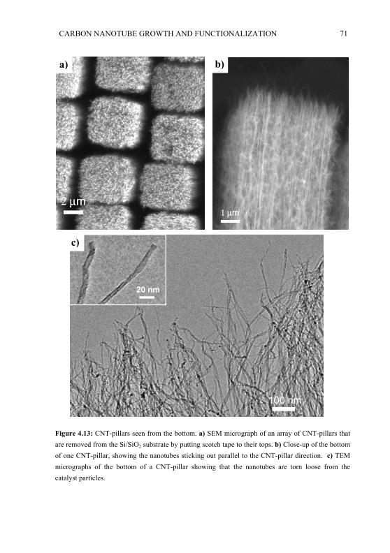
CARBON NANOTUBE GROWTH AND FUNCTIONALIZATION 71
b)a)
c)
Figure 4.13: CNT-pillars seen from the bottom. a) SEM micrograph of an array of CNT-pillars that are removed from the Si/SiO2 substrate by putting scotch tape to their tops. b) Close-up of the bottom of one CNT-pillar, showing the nanotubes sticking out parallel to the CNT-pillar direction. c) TEMmicrographs of the bottom of a CNT-pillar showing that the nanotubes are torn loose from the catalyst particles.
SEM micrograph is shown of 35 m long CNT-pillars that have been removed from the
72
SEM micrograph is shown of 35 m long CNT-pillars that have been removed from the Si/SiO2 substrate by carefully taping the tops of the CNT-pillars. Thus in the micrograph we see the bottoms of the CNT-pillars, where they were attached to the Si/SiO2 substrate. The ordered pattern of square CNT-pillars is well preserved. The nanotubes end as sharp points that are almost parallel to the CNT-pillar direction (compared to the nanotube ends at the top of the CNT-pillars), as can be seen in Fig. 4.13(b). In Fig. 4.13(c) a TEM micrograph of the bottom of a CNT-pillar is depicted. At the bottom of the nanotubes no catalyst particles are found either, so when removing the CNT-pillars from the substrate they are effectively torn off the catalyst particles, which stay behind on the substrate. No remaining nanotube parts were observed on the substrate after removing the nanotube pillars. After removal from the substrate one thus has a large amount of pure nanotubes without encapsulated catalyst particles and without evidence of the presence of amorphous carbon between or attached to the nanotubes. This eliminates the necessity of purification.
The taping technique has also been used to create electric contact to the nanotubes by using an adhesive tape that has an electrically conductive adhesive (3M, 1181). The electric contact improved when 50 nm gold had been evaporated on the tops of long CNT-pillars (see also section 4.3.1.2) before they were brought in contact with the adhesive tape. The electric contact obtained by this method was good enough to perform field emission measurements on the well aligned nanotubes in the bottoms of the CNT-pillars. The field emission measurements however showed that the CNT-pillar bottoms were not among the best field emitters and therefore the results of these measurements will not be discussed in further detail.
4.2.2 Detailed description of CNT-pillar growth
4.2.2.1 Procedure for growing CNT-pillars
The technique used by Bonard et al [104] for the growth of regular carbon nanotubes, has been modified and optimized for the growth of CNT-pillars.
Spin coating
A first small modification is that the ferritin containing ink (a solution of 500 g/ml ferritin + 50 mMol Al(NO3)3·9H2O in demineralized water) is spin coated on the polymer stamp instead of blown off by a nitrogen gun. It turned out that the growth of the CNT-pillars is sensitive to the way the ink is removed from and dried on the stamp. With the
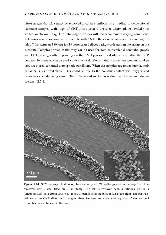
CARBON NANOTUBE GROWTH AND FUNCTIONALIZATION 73
nitrogen gun the ink cannot be removed/dried in a uniform way, leading to conventionalnanotube samples with rings of CNT-pillars around the spot where ink removal/dryingstarted, as shown in Fig. 4.14. The rings are areas with the same removal/drying conditions. A homogeneous coverage of the sample with CNT-pillars can be obtained by spinning the ink off the stamp at 360 rpm for 30 seconds and directly afterwards putting the stamp on the substrate. Samples printed in this way can be used for both conventional nanotube growth and CNT-pillar growth, depending on the CVD process used afterwards. After the CPprocess, the samples can be used up to one week after printing without any problems, when they are stored at normal atmospheric conditions. When the samples age to one month, theirbehavior is less predictable. This could be due to the constant contact with oxygen and water vapor while being stored. The influence of oxidation is discussed below and also in section 4.2.2.2.
Figure 4.14: SEM micrograph showing the sensitivity of CNT-pillar growth to the way the ink isremoved from - and dried on - the stamp. The ink is removed with a nitrogen gun in a (undeliberately) non-continuous way, in the direction from the bottom-left to top-right. The contrast-rich rings are CNT-pillars and the grey rings between are areas with squares of conventionalnanotubes, as can be seen in the inset.
74
Oxygen exposure
An important modification for the CNT-pillar growth is the exposure of the sample to O2 while heating up before starting the real CVD process. After inserting the sample into the hot part of the furnace, the furnace is pumped till the pressure reaches about 2·10-2 mbar, which takes 40 to 50 seconds. Then the sample is exposed to a typically 0.1 mbar O2
atmosphere during 30 seconds (while the sample is heating up). Finally the oxygen is pumped away and the CVD process is started, as usually, 2 minutes after insertion of the sample into the furnace.
Why oxygen exposure causes the big difference between conventional nanotubes and vertically aligned nanotubes is not clear. Emmenegger et al [117] have investigated the transformation of ferric nitrate catalyst, Fe(NO3)3, during nanotube growth by CVD of acetylene. The Fe(NO3)3 transforms into Fe2O3 during pre-heating without acetylene. After exposure to acetylene a reduction to Fe3O4 and FeO takes place followed by a transformation to Fe3C from which the Fe clusters form on which the nanotubes grow. Ferritin cores consist of crystalline ferrihydrate (FeOOH), which will presumably undergo a similar transformation trajectory. It could be that additional oxygen leads to different intermediate iron oxides on which acetylene can be decomposed faster or in a better way. Acetylene is thermally stable at temperatures below 800° C and therefore needs iron oxide particles that function as catalyst for the dissociation of acetylene at the first CVD stage. Insitu high temperature X-ray measurements similar to Emmenegger et al [117] could give an answer about a possibly different transformation trajectory between the growth of CNT-pillars and the growth of conventional nanotubes. It could also be that additional oxygen influences the formation of the facets of well defined crystallographic orientation on the Fe particles, which are needed for the catalytic dissociation of acetylene during the CNT growth [118]. The exact geometry of the iron particles influences the diffusion of carbon through the particles, which in turn determines the final length of the nanotube [99], which is one of the main differences between the CNT-pillars and the conventional nanotubes. Another possibility would be that oxygen is needed to effectively burn away the polypeptide chains that are enclosing the iron containing ferritin core. The free cores can then be reduced by the acetylene to pure iron.
4.2.2.2 Length control and growth rate
The CNT-pillars discussed in this chapter can be grown to any desired length, by choosing a correct combination of CVD temperature, CVD duration and amount of oxygen supplied to the sample before CVD start. In an ideal case it would be possible to monitor the
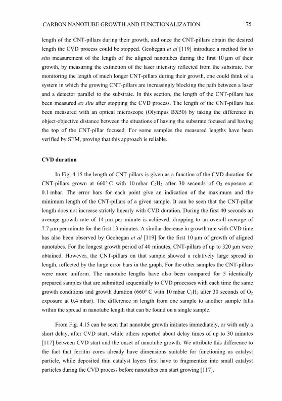
CARBON NANOTUBE GROWTH AND FUNCTIONALIZATION 75
length of the CNT-pillars during their growth, and once the CNT-pillars obtain the desired length the CVD process could be stopped. Geohegan et al [119] introduce a method for in situ measurement of the length of the aligned nanotubes during the first 10 m of their growth, by measuring the extinction of the laser intensity reflected from the substrate. For monitoring the length of much longer CNT-pillars during their growth, one could think of a system in which the growing CNT-pillars are increasingly blocking the path between a laser and a detector parallel to the substrate. In this section, the length of the CNT-pillars has been measured ex situ after stopping the CVD process. The length of the CNT-pillars has been measured with an optical microscope (Olympus BX50) by taking the difference in object-objective distance between the situations of having the substrate focused and having the top of the CNT-pillar focused. For some samples the measured lengths have been verified by SEM, proving that this approach is reliable.
CVD duration
In Fig. 4.15 the length of CNT-pillars is given as a function of the CVD duration for CNT-pillars grown at 660° C with 10 mbar C2H2 after 30 seconds of O2 exposure at 0.1 mbar. The error bars for each point give an indication of the maximum and the minimum length of the CNT-pillars of a given sample. It can be seen that the CNT-pillar length does not increase strictly linearly with CVD duration. During the first 40 seconds an average growth rate of 14 m per minute is achieved, dropping to an overall average of 7.7 m per minute for the first 13 minutes. A similar decrease in growth rate with CVD time has also been observed by Geohegan et al [119] for the first 10 m of growth of aligned nanotubes. For the longest growth period of 40 minutes, CNT-pillars of up to 320 m were obtained. However, the CNT-pillars on that sample showed a relatively large spread in length, reflected by the large error bars in the graph. For the other samples the CNT-pillars were more uniform. The nanotube lengths have also been compared for 5 identically prepared samples that are submitted sequentially to CVD processes with each time the same growth conditions and growth duration (660° C with 10 mbar C2H2 after 30 seconds of O2
exposure at 0.4 mbar). The difference in length from one sample to another sample falls within the spread in nanotube length that can be found on a single sample.
From Fig. 4.15 can be seen that nanotube growth initiates immediately, or with only a short delay, after CVD start, while others reported about delay times of up to 30 minutes [117] between CVD start and the onset of nanotube growth. We attribute this difference to the fact that ferritin cores already have dimensions suitable for functioning as catalyst particle, while deposited thin catalyst layers first have to fragmentize into small catalyst particles during the CVD process before nanotubes can start growing [117].
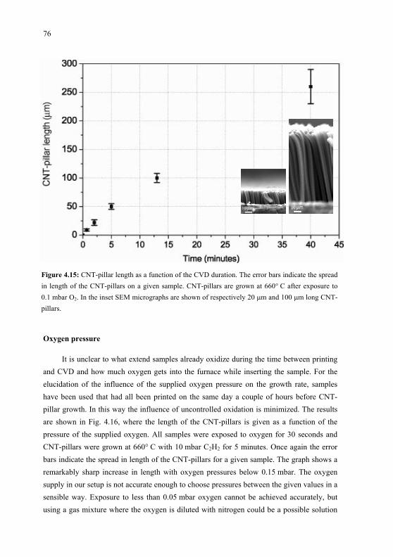
76
Figure 4.15: CNT-pillar length as a function of the CVD duration. The error bars indicate the spread in length of the CNT-pillars on a given sample. CNT-pillars are grown at 660° C after exposure to0.1 mbar O2. In the inset SEM micrographs are shown of respectively 20 m and 100 m long CNT-pillars.
Oxygen pressure
It is unclear to what extend samples already oxidize during the time between printing and CVD and how much oxygen gets into the furnace while inserting the sample. For the elucidation of the influence of the supplied oxygen pressure on the growth rate, sampleshave been used that had all been printed on the same day a couple of hours before CNT-pillar growth. In this way the influence of uncontrolled oxidation is minimized. The results are shown in Fig. 4.16, where the length of the CNT-pillars is given as a function of thepressure of the supplied oxygen. All samples were exposed to oxygen for 30 seconds and CNT-pillars were grown at 660° C with 10 mbar C2H2 for 5 minutes. Once again the errorbars indicate the spread in length of the CNT-pillars for a given sample. The graph shows aremarkably sharp increase in length with oxygen pressures below 0.15 mbar. The oxygen supply in our setup is not accurate enough to choose pressures between the given values in a sensible way. Exposure to less than 0.05 mbar oxygen cannot be achieved accurately, but using a gas mixture where the oxygen is diluted with nitrogen could be a possible solution
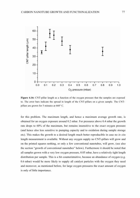
CARBON NANOTUBE GROWTH AND FUNCTIONALIZATION 77
Figure 4.16: CNT-pillar length as a function of the oxygen pressure that the samples are exposedto. The error bars indicate the spread in length of the CNT-pillars on a given sample. The CNT-pillars are grown for 5 minutes at 660° C.
for this problem. The maximum length, and hence a maximum average growth rate, is obtained for an oxygen exposure around 0.2 mbar. For pressures above 0.4 mbar the growth rate drops to 60% of the maximum, but remains insensitive to the exact oxygen pressure (and hence also less sensitive to pumping capacity and to oxidation during sample storage etc). This makes the growth to a desired length much better reproducible in case no in situlength measurement is available. Without any oxygen supply no CNT-pillars will grow and on the printed squares nothing, or only a few conventional nanotubes, will grow, (see alsothe section “growth of conventional nanotubes” below). Furthermore it should be noted that all samples grown with a very low oxygen pressure, 0.05 mbar, have a relatively tight length distribution per sample. This is a bit counterintuitive, because an abundance of oxygen (e.g. 0.6 mbar) would be more likely to supply all catalyst particles with the oxygen they needand moreover, as mentioned before, for large oxygen pressures the exact amount of oxygen is only of little importance.
78
Acetylene pressure
The acetylene pressure during CVD has been varied for CNT-pillars grown at 660° C for 5 minutes, after 0.1 mbar O2 for 30 s. Differences in the length of the CNT-pillars, grown with 2, 5, 10 and 20 mbar C2H2, all fall within the experimental error. The only difference is that the samples grown with 10 mbar and 20 mbar have a slightly better homogeneity than the samples grown at lower pressures. It can be concluded that the CNT-pillar growth at these acetylene pressures is not limited by the supply of acetylene, but is limited by diffusion of carbon through the catalyst particles [105].
Acetylene flow
In contrast to the small influence of the acetylene pressure, the acetylene flow is decisive for the CNT-pillar growth. Between the pump and the valve that is used for starting and stopping pumping the furnace, we have installed a second valve. This valve (a Leybold valve type EV 025 SA) can be opened in discrete steps. With the valve completely opened we obtain samples that are covered with more than 90% CNT-pillars (this holds for growth conditions: 660° C, 20 mbar C2H2 for 5 minutes, after 0.1 mbar O2 for 30 s). When the acetylene flux is reduced, the coverage is perfectly homogeneous apart from a few small empty spots where no squares were printed because of imperfections during the CPprinting. When the acetylene flux is reduced even more, the whole sample is a half-half mixture of CNT-pillars and conventional nanotubes. To get an impression about the difference in flow speed for the three valve positions, we measured the time it takes to pump the furnace, filled with nitrogen, from 300 mbar to 1 mbar. The average times found were respectively 10.5 s, 10.7 s and 11.2 s, which shows that the pumping capacity is changed only by a small amount. Apparently the speed with which the acetylene flows through the quartz tube of the furnace has a very strong influence on the CNT-pillar growth. Either a continuous supply of new C2H2 molecules is the important factor, or the time available for the C2H2 molecules to dissociate on the catalyst particles, or the removal of hydrogen that is generated as a by-product during dissociation of acetylene, or an interplay of these factors. The optimization of the flow conditions presented here is setup-dependent, although the importance of the flow conditions to the result will be general. The dimensions of the furnace and the pumping capacity of the pump influence the flow conditions to a large extend. And for a given setup also a different CVD temperature will very likely have a different optimal flow condition. Another way to change the flow conditions in the furnace is by using different mixtures of acetylene with a carrier gas, for instance nitrogen [117] or hydrogen [120].
CARBON NANOTUBE GROWTH AND FUNCTIONALIZATION 79
CVD temperature
CNT-pillars can grow really fast at temperatures higher than 660° C (144 m after 5 minutes has been achieved for samples grown at 720° C) but then reproducibility is a problem and many times the CNT-pillar coverage is just 10% or less. Some spots on the sample are favored for the fast growing CNT-pillars, notably around open spots in the printed pattern and at the edges of the sample. These samples often show big differences in CNT-pillar lengths, which is caused by inhomogeneities in the CP printing procedure. Growing samples at 660° C is much more forgiving and results in homogeneous CNT-pillars in spite of inhomogeneities in the CP structure on the substrate. Also for higher CVD temperatures, growth conditions may exist that give good homogeneously covered samples, but these conditions have not been found yet. Above 800° C acetylene will dissociate without the need of a catalyst, resulting in deposition of amorphous carbon on the sample next to nanotube growth.
Ferritin concentration
The ferritin concentration has proven not to be very important for the growth of CNT-pillars, as long as it exceeds 100 g/ml. Below 100 g/ml ferritin concentration (using the same 50 mMol aluminum nitrate concentration) neither CNT-pillars nor conventional nanotubes will grow well. Using a 150 g/ml ferritin solution instead of a 500 g/ml ferritin solution does not result in a difference in the CNT-pillars being grown. There is neither a difference in the length of the CNT-pillars, nor a difference in the amount of nanotubes within a CNT-pillar. The amount of ferritin cores at the surface of the printed squares that actually participate in the CNT-pillar growth is probably limited to a maximum number, which is already achieved with 100 g/ml ferritin ink.
4.2.2.3 Growth of conventional nanotubes
Exposure to oxygen is usually also necessary for the growth of conventional nanotubes (like the ones depicted before in Fig. 4.10(a)) using a ferritin ink. Without oxygen exposure the printed squares hardly develop, meaning that only a few nanotubes (or none) grow on the printed squares. This was not the case for the nanotubes grown by Bonard et al[104] even though we used the same growth process and the very same furnace, but with a slightly better pump. We assume that slower pumping in Bonard’s case caused the sample during heat-up to be exposed to an amount of oxygen just sufficient to obtain well developed squares with conventional nanotubes. For growing well developed squares in our
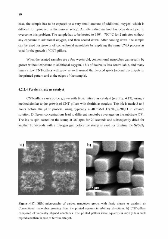
80
case, the sample has to be exposed to a very small amount of additional oxygen, which isdifficult to reproduce in the current set-up. An alternative method has been developed to overcome this problem. The sample has to be heated to 650° - 700° C for 2 minutes without any exposure to additional oxygen, and then cooled down. After cooling down, the samplecan be used for growth of conventional nanotubes by applying the same CVD process as used for the growth of CNT-pillars.
When the printed samples are a few weeks old, conventional nanotubes can usually be grown without exposure to additional oxygen. This of course is less controllable, and manytimes a few CNT-pillars will grow as well around the favored spots (around open spots inthe printed pattern and at the edges of the sample).
4.2.2.4 Ferric nitrate as catalyst
CNT-pillars can also be grown with ferric nitrate as catalyst (see Fig. 4.17), using a method similar to the growth of CNT-pillars with ferritin as catalyst. The ink is made 3 to 6 hours before the CP process, using typically a 40 mMol Fe(NO3)3·9H2O in ethanol solution. Different concentrations lead to different nanotube coverages on the substrate [79]. The ink is spin coated on the stamp at 360 rpm for 20 seconds and subsequently dried for another 10 seconds with a nitrogen gun before the stamp is used for printing the Si/SiO2
a) b)
Figure 4.17: SEM micrographs of carbon nanotubes grown with ferric nitrate as catalyst. a)Conventional nanotubes growing from the printed squares in arbitrary directions. b) CNT-pillars composed of vertically aligned nanotubes. The printed pattern (here squares) is mostly less well reproduced than in case of ferritin catalyst.
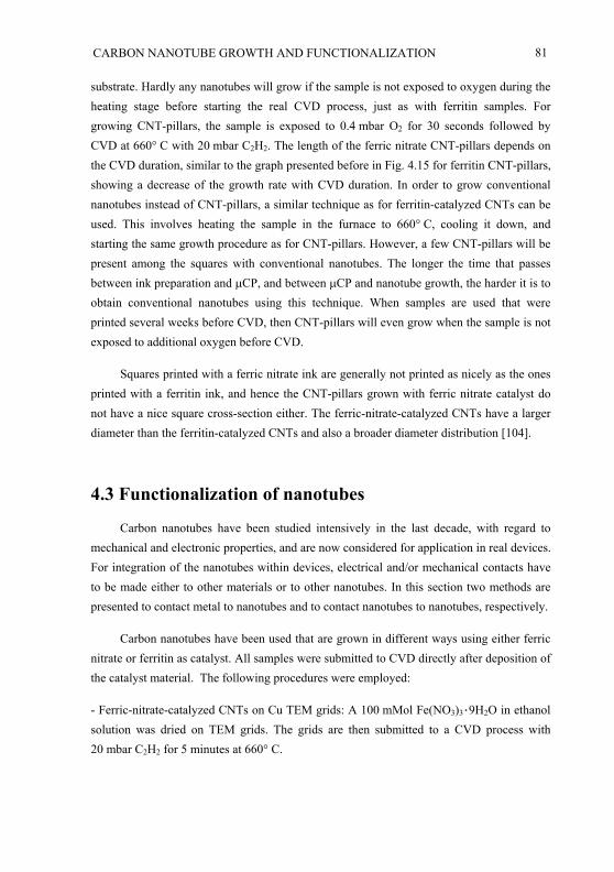
CARBON NANOTUBE GROWTH AND FUNCTIONALIZATION 81
substrate. Hardly any nanotubes will grow if the sample is not exposed to oxygen during the heating stage before starting the real CVD process, just as with ferritin samples. For growing CNT-pillars, the sample is exposed to 0.4 mbar O2 for 30 seconds followed by CVD at 660° C with 20 mbar C2H2. The length of the ferric nitrate CNT-pillars depends on the CVD duration, similar to the graph presented before in Fig. 4.15 for ferritin CNT-pillars, showing a decrease of the growth rate with CVD duration. In order to grow conventional nanotubes instead of CNT-pillars, a similar technique as for ferritin-catalyzed CNTs can be used. This involves heating the sample in the furnace to 660° C, cooling it down, and starting the same growth procedure as for CNT-pillars. However, a few CNT-pillars will be present among the squares with conventional nanotubes. The longer the time that passes between ink preparation and CP, and between CP and nanotube growth, the harder it is to obtain conventional nanotubes using this technique. When samples are used that were printed several weeks before CVD, then CNT-pillars will even grow when the sample is not exposed to additional oxygen before CVD.
Squares printed with a ferric nitrate ink are generally not printed as nicely as the ones printed with a ferritin ink, and hence the CNT-pillars grown with ferric nitrate catalyst do not have a nice square cross-section either. The ferric-nitrate-catalyzed CNTs have a larger diameter than the ferritin-catalyzed CNTs and also a broader diameter distribution [104].
4.3 Functionalization of nanotubes
Carbon nanotubes have been studied intensively in the last decade, with regard to mechanical and electronic properties, and are now considered for application in real devices. For integration of the nanotubes within devices, electrical and/or mechanical contacts have to be made either to other materials or to other nanotubes. In this section two methods are presented to contact metal to nanotubes and to contact nanotubes to nanotubes, respectively.
Carbon nanotubes have been used that are grown in different ways using either ferric nitrate or ferritin as catalyst. All samples were submitted to CVD directly after deposition of the catalyst material. The following procedures were employed:
- Ferric-nitrate-catalyzed CNTs on Cu TEM grids: A 100 mMol Fe(NO3)3·9H2O in ethanol solution was dried on TEM grids. The grids are then submitted to a CVD process with 20 mbar C2H2 for 5 minutes at 660° C.
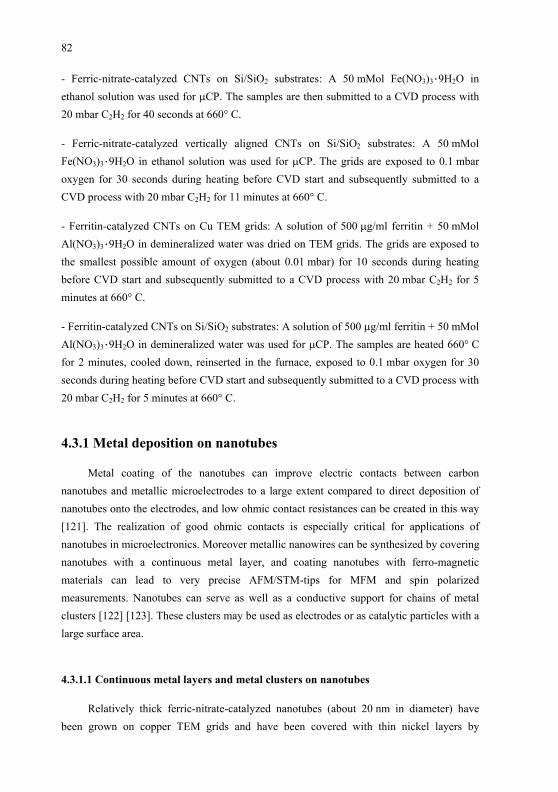
82
- Ferric-nitrate-catalyzed CNTs on Si/SiO2 substrates: A 50 mMol Fe(NO3)3·9H2O in ethanol solution was used for CP. The samples are then submitted to a CVD process with 20 mbar C2H2 for 40 seconds at 660° C.
- Ferric-nitrate-catalyzed vertically aligned CNTs on Si/SiO2 substrates: A 50 mMol Fe(NO3)3·9H2O in ethanol solution was used for CP. The grids are exposed to 0.1 mbar oxygen for 30 seconds during heating before CVD start and subsequently submitted to a CVD process with 20 mbar C2H2 for 11 minutes at 660° C.
- Ferritin-catalyzed CNTs on Cu TEM grids: A solution of 500 g/ml ferritin + 50 mMol Al(NO3)3·9H2O in demineralized water was dried on TEM grids. The grids are exposed to the smallest possible amount of oxygen (about 0.01 mbar) for 10 seconds during heating before CVD start and subsequently submitted to a CVD process with 20 mbar C2H2 for 5 minutes at 660° C.
- Ferritin-catalyzed CNTs on Si/SiO2 substrates: A solution of 500 g/ml ferritin + 50 mMol Al(NO3)3·9H2O in demineralized water was used for CP. The samples are heated 660° C for 2 minutes, cooled down, reinserted in the furnace, exposed to 0.1 mbar oxygen for 30 seconds during heating before CVD start and subsequently submitted to a CVD process with 20 mbar C2H2 for 5 minutes at 660° C.
4.3.1 Metal deposition on nanotubes
Metal coating of the nanotubes can improve electric contacts between carbon nanotubes and metallic microelectrodes to a large extent compared to direct deposition of nanotubes onto the electrodes, and low ohmic contact resistances can be created in this way [121]. The realization of good ohmic contacts is especially critical for applications of nanotubes in microelectronics. Moreover metallic nanowires can be synthesized by covering nanotubes with a continuous metal layer, and coating nanotubes with ferro-magnetic materials can lead to very precise AFM/STM-tips for MFM and spin polarized measurements. Nanotubes can serve as well as a conductive support for chains of metal clusters [122] [123]. These clusters may be used as electrodes or as catalytic particles with a large surface area.
4.3.1.1 Continuous metal layers and metal clusters on nanotubes
Relatively thick ferric-nitrate-catalyzed nanotubes (about 20 nm in diameter) have been grown on copper TEM grids and have been covered with thin nickel layers by
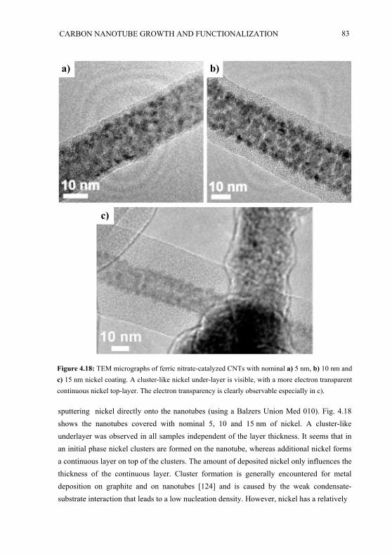
CARBON NANOTUBE GROWTH AND FUNCTIONALIZATION 83
a) b)
c)
Figure 4.18: TEM micrographs of ferric nitrate-catalyzed CNTs with nominal a) 5 nm, b) 10 nm andc) 15 nm nickel coating. A cluster-like nickel under-layer is visible, with a more electron transparent continuous nickel top-layer. The electron transparency is clearly observable especially in c).
sputtering nickel directly onto the nanotubes (using a Balzers Union Med 010). Fig. 4.18 shows the nanotubes covered with nominal 5, 10 and 15 nm of nickel. A cluster-likeunderlayer was observed in all samples independent of the layer thickness. It seems that in an initial phase nickel clusters are formed on the nanotube, whereas additional nickel formsa continuous layer on top of the clusters. The amount of deposited nickel only influences the thickness of the continuous layer. Cluster formation is generally encountered for metaldeposition on graphite and on nanotubes [124] and is caused by the weak condensate-substrate interaction that leads to a low nucleation density. However, nickel has a relatively
84
strong interaction with the graphite-like nanotube surface, which is attributed to curvature-induced rehybridization of carbon sp2 orbitals with the Ni d-orbital [125]. Therefore Nideposition on nanotubes leads to a more homogeneous coverage than for instance Au deposition (cf. Fig. 4.20). An interesting observation is the difference in contrast between the dark cluster-like underlayer and the more electron transparent top layer. Comparison with TEM images of nickel in other publications, it could be possible that the dark imaged
a)
b) c)
Figure 4.19: TEM micrographs of ferritin-catalyzed CNTs with a nickel coating. a) Nominal 7 nmnickel layer, showing small clusters with a high nucleation density. b) and c) The nickel layer after heating to respectively 660° C and 800° C for 2 minutes minutes (ex situ). Larger clusters coexistwith segments of continuous coating on the nanotube.
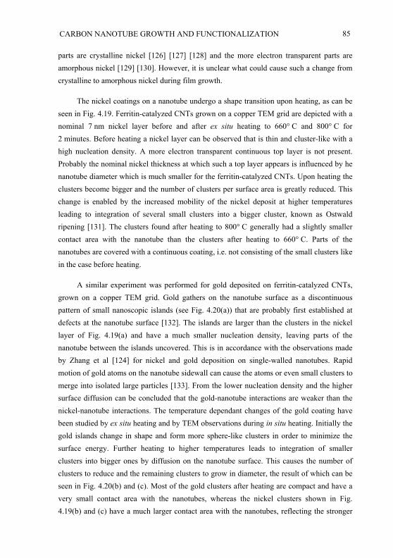
CARBON NANOTUBE GROWTH AND FUNCTIONALIZATION 85
parts are crystalline nickel [126] [127] [128] and the more electron transparent parts are amorphous nickel [129] [130]. However, it is unclear what could cause such a change from crystalline to amorphous nickel during film growth.
The nickel coatings on a nanotube undergo a shape transition upon heating, as can be seen in Fig. 4.19. Ferritin-catalyzed CNTs grown on a copper TEM grid are depicted with a nominal 7 nm nickel layer before and after ex situ heating to 660° C and 800° C for 2 minutes. Before heating a nickel layer can be observed that is thin and cluster-like with a high nucleation density. A more electron transparent continuous top layer is not present. Probably the nominal nickel thickness at which such a top layer appears is influenced by he nanotube diameter which is much smaller for the ferritin-catalyzed CNTs. Upon heating the clusters become bigger and the number of clusters per surface area is greatly reduced. This change is enabled by the increased mobility of the nickel deposit at higher temperatures leading to integration of several small clusters into a bigger cluster, known as Ostwald ripening [131]. The clusters found after heating to 800° C generally had a slightly smaller contact area with the nanotube than the clusters after heating to 660° C. Parts of the nanotubes are covered with a continuous coating, i.e. not consisting of the small clusters like in the case before heating.
A similar experiment was performed for gold deposited on ferritin-catalyzed CNTs, grown on a copper TEM grid. Gold gathers on the nanotube surface as a discontinuous pattern of small nanoscopic islands (see Fig. 4.20(a)) that are probably first established at defects at the nanotube surface [132]. The islands are larger than the clusters in the nickel layer of Fig. 4.19(a) and have a much smaller nucleation density, leaving parts of the nanotube between the islands uncovered. This is in accordance with the observations made by Zhang et al [124] for nickel and gold deposition on single-walled nanotubes. Rapid motion of gold atoms on the nanotube sidewall can cause the atoms or even small clusters to merge into isolated large particles [133]. From the lower nucleation density and the higher surface diffusion can be concluded that the gold-nanotube interactions are weaker than the nickel-nanotube interactions. The temperature dependant changes of the gold coating have been studied by ex situ heating and by TEM observations during in situ heating. Initially the gold islands change in shape and form more sphere-like clusters in order to minimize the surface energy. Further heating to higher temperatures leads to integration of smaller clusters into bigger ones by diffusion on the nanotube surface. This causes the number of clusters to reduce and the remaining clusters to grow in diameter, the result of which can be seen in Fig. 4.20(b) and (c). Most of the gold clusters after heating are compact and have a very small contact area with the nanotubes, whereas the nickel clusters shown in Fig. 4.19(b) and (c) have a much larger contact area with the nanotubes, reflecting the stronger
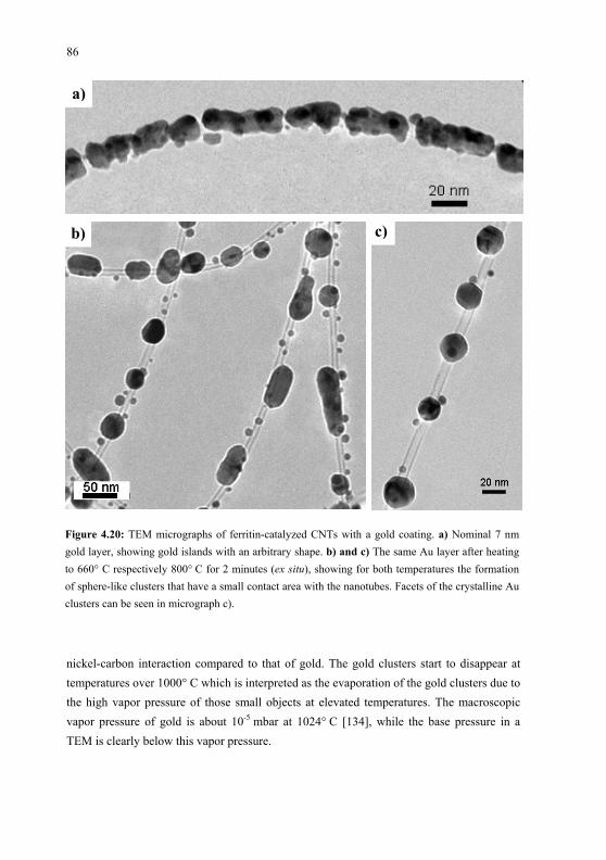
86
a)
c)b)
Figure 4.20: TEM micrographs of ferritin-catalyzed CNTs with a gold coating. a) Nominal 7 nmgold layer, showing gold islands with an arbitrary shape. b) and c) The same Au layer after heatingto 660° C respectively 800° C for 2 minutes (ex situ), showing for both temperatures the formationof sphere-like clusters that have a small contact area with the nanotubes. Facets of the crystalline Auclusters can be seen in micrograph c).
nickel-carbon interaction compared to that of gold. The gold clusters start to disappear at temperatures over 1000° C which is interpreted as the evaporation of the gold clusters due to the high vapor pressure of those small objects at elevated temperatures. The macroscopicvapor pressure of gold is about 10-5 mbar at 1024° C [134], while the base pressure in aTEM is clearly below this vapor pressure.
CARBON NANOTUBE GROWTH AND FUNCTIONALIZATION 87
4.3.1.2 Partial coating of nanotubes
In a next step we developed an easy method for creating large numbers of nanotubes that are coated only on one end, leaving the rest of the nanotube uncoated. Ferric-nitrate-catalyzed vertically aligned CNTs have been grown on a Si/SiO2 substrate, which resulted in 35 m long aligned nanotubes of about 20 nm diameter. When metals are evaporated on top of the vertically aligned nanotubes, then only the top parts are covered, because the dense packing prevents the metal from reaching the center and lower parts of the nanotubes. The partly coated nanotubes have been taken off the substrate, sonicated (Branson 2510) in ethanol for 30 minutes and afterwards deposited from solution onto a carbon coated copper TEM grid. In Fig. 4.21 a TEM micrograph is given of a nickel coated end of a nanotube together with uncoated parts of two other nanotubes. The nanotube considered here has a nickel coated part extending for 2 m (with variations in nickel coverage), but that differs from nanotube to nanotube. This is caused by the fact that our “aligned” nanotubes are not
Figure 4.21: TEM micrograph of a nickel coated nanotube end (on the right-hand side) and two uncoated nanotube parts (on the left-hand side) deposited on a carbon coated TEM grid. The low contrast of the uncoated parts is caused by the carbon background.
88
straight, resulting in variations in lengths of the parts that are exposed to nickel in the deposition process. When straight vertically aligned nanotubes are being used that have uniform lengths [113] [112], then nanotubes could be coated on a single end in a better defined way and by millions or billions at a time.
This experiment moreover demonstrates that sputtered nickel coatings attach strong enough to nanotubes to endure sonication. This method for metal deposition on a single end has only been tested for nickel so far, but can basically be used for any metal that attaches strong enough to nanotubes to endure sonication. Experiments done by Zhang et al [124] show that Pd and Ti have comparable or even better metal-nanotube interaction than Ni. Therefore it should be possible to use this method for Pd and Ti as well. On the contrary Au, Al and Fe have only weak interactions with nanotubes and might not endure sonication. However, straight aligned nanotubes that are not entangled could probably be brought into solution in a more gentle way than sonication.
4.3.2 Growth of secondary nanotubes
In this section the direct growth of carbon nanotubes on the sidewalls of carbon nanotubes is presented. If nanotubes are cross-linked and thereby establish a stable binding it should be possible to create very strong polymer compound materials. The nanotube-nanotube bonding could maybe be reinforced by annealing (creating atomic bonds between the graphitic layers). Of course the network can also be further cross-linked by tertiary connections (nanotubes on nanotubes on nanotubes) and so forth. With proper steering, this method of connecting nanotubes is of potential interest for growing nanotube networks for microelectronics.
4.3.2.1 Secondary nanotubes using nickel catalyst
Iron, cobalt and nickel are known to be good catalysts for the growth of carbon nanotubes by CVD. Even thin layers of these metals can be used for growing nanotubes because the thin layer will fragmentize into small clusters when heated, as demonstrated above (see Fig. 4.19). We used nickel coated carbon nanotubes to grow secondary carbon nanotubes on the sidewalls of primary carbon nanotubes. Ferric-nitrate-catalyzed CNTs were grown on molybdenum TEM grids, a nominal 5 nm nickel layer was sputtered on the primary nanotubes and the sample was re-submitted to the same standard CVD process (20 mbar C2H2, 5 minutes at 660° C). As a result, secondary nanotubes were obtained on the sidewalls of the primary nanotubes, as can be seen in Fig. 4.22(a). The secondary nanotubes
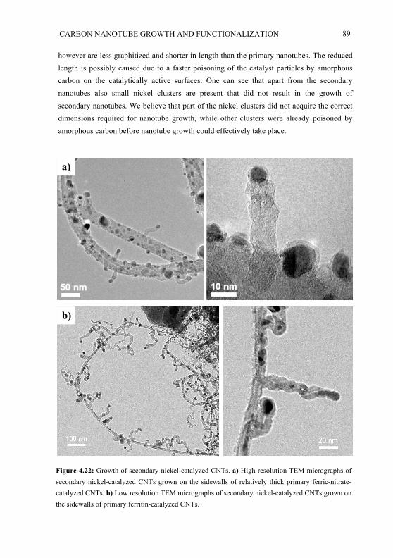
CARBON NANOTUBE GROWTH AND FUNCTIONALIZATION 89
however are less graphitized and shorter in length than the primary nanotubes. The reduced length is possibly caused due to a faster poisoning of the catalyst particles by amorphouscarbon on the catalytically active surfaces. One can see that apart from the secondary nanotubes also small nickel clusters are present that did not result in the growth of secondary nanotubes. We believe that part of the nickel clusters did not acquire the correct dimensions required for nanotube growth, while other clusters were already poisoned by amorphous carbon before nanotube growth could effectively take place.
a)
b)
Figure 4.22: Growth of secondary nickel-catalyzed CNTs. a) High resolution TEM micrographs ofsecondary nickel-catalyzed CNTs grown on the sidewalls of relatively thick primary ferric-nitrate-catalyzed CNTs. b) Low resolution TEM micrographs of secondary nickel-catalyzed CNTs grown onthe sidewalls of primary ferritin-catalyzed CNTs.
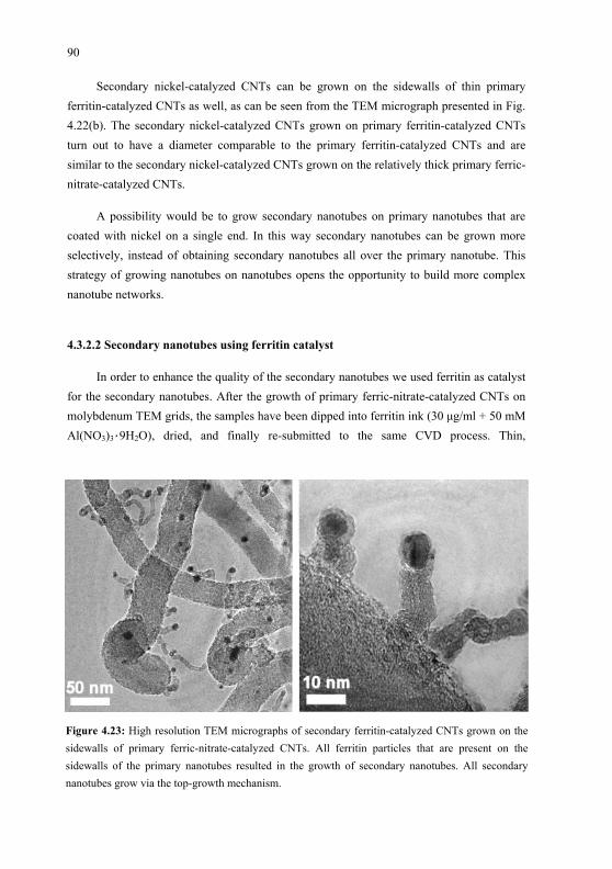
90
Secondary nickel-catalyzed CNTs can be grown on the sidewalls of thin primaryferritin-catalyzed CNTs as well, as can be seen from the TEM micrograph presented in Fig. 4.22(b). The secondary nickel-catalyzed CNTs grown on primary ferritin-catalyzed CNTsturn out to have a diameter comparable to the primary ferritin-catalyzed CNTs and are similar to the secondary nickel-catalyzed CNTs grown on the relatively thick primary ferric-nitrate-catalyzed CNTs.
A possibility would be to grow secondary nanotubes on primary nanotubes that arecoated with nickel on a single end. In this way secondary nanotubes can be grown moreselectively, instead of obtaining secondary nanotubes all over the primary nanotube. This strategy of growing nanotubes on nanotubes opens the opportunity to build more complexnanotube networks.
4.3.2.2 Secondary nanotubes using ferritin catalyst
In order to enhance the quality of the secondary nanotubes we used ferritin as catalyst for the secondary nanotubes. After the growth of primary ferric-nitrate-catalyzed CNTs on molybdenum TEM grids, the samples have been dipped into ferritin ink (30 µg/ml + 50 mM Al(NO3)3·9H2O), dried, and finally re-submitted to the same CVD process. Thin,
Figure 4.23: High resolution TEM micrographs of secondary ferritin-catalyzed CNTs grown on thesidewalls of primary ferric-nitrate-catalyzed CNTs. All ferritin particles that are present on the sidewalls of the primary nanotubes resulted in the growth of secondary nanotubes. All secondary nanotubes grow via the top-growth mechanism.
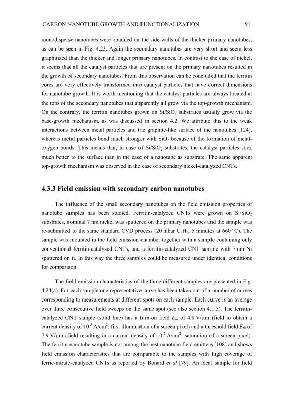
CARBON NANOTUBE GROWTH AND FUNCTIONALIZATION 91
monodisperse nanotubes were obtained on the side walls of the thicker primary nanotubes, as can be seen in Fig. 4.23. Again the secondary nanotubes are very short and seem less graphitized than the thicker and longer primary nanotubes. In contrast to the case of nickel, it seems that all the catalyst particles that are present on the primary nanotubes resulted in the growth of secondary nanotubes. From this observation can be concluded that the ferritin cores are very effectively transformed into catalyst particles that have correct dimensions for nanotube growth. It is worth mentioning that the catalyst particles are always located at the tops of the secondary nanotubes that apparently all grow via the top-growth mechanism. On the contrary, the ferritin nanotubes grown on Si/SiO2 substrates usually grow via the base-growth mechanism, as was discussed in section 4.2. We attribute this to the weak interactions between metal particles and the graphite-like surface of the nanotubes [124], whereas metal particles bond much stronger with SiO2 because of the formation of metal-oxygen bonds. This means that, in case of Si/SiO2 substrates, the catalyst particles stick much better to the surface than in the case of a nanotube as substrate. The same apparent top-growth mechanism was observed in the case of secondary nickel-catalyzed CNTs.
4.3.3 Field emission with secondary carbon nanotubes
The influence of the small secondary nanotubes on the field emission properties of nanotube samples has been studied. Ferritin-catalyzed CNTs were grown on Si/SiO2
substrates, nominal 7 nm nickel was sputtered on the primary nanotubes and the sample was re-submitted to the same standard CVD process (20 mbar C2H2, 5 minutes at 660° C). The sample was mounted in the field emission chamber together with a sample containing only conventional ferritin-catalyzed CNTs, and a ferritin-catalyzed CNT sample with 7 nm Ni sputtered on it. In this way the three samples could be measured under identical conditions for comparison.
The field emission characteristics of the three different samples are presented in Fig. 4.24(a). For each sample one representative curve has been taken out of a number of curves corresponding to measurements at different spots on each sample. Each curve is an average over three consecutive field sweeps on the same spot (see also section 4.1.5). The ferritin-catalyzed CNT sample (solid line) has a turn-on field Eto of 4.8 V/ m (field to obtain a current density of 10-5 A/cm2; first illumination of a screen pixel) and a threshold field Eth of 7.9 V/ m (field resulting in a current density of 10-2 A/cm2; saturation of a screen pixel). The ferritin nanotube sample is not among the best nanotube field emitters [108] and shows field emission characteristics that are comparable to the samples with high coverage of ferric-nitrate-catalyzed CNTs as reported by Bonard et al [79]. An ideal sample for field
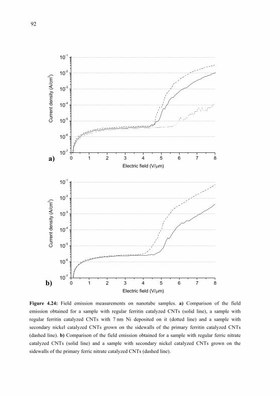
92
a)
b)
Figure 4.24: Field emission measurements on nanotube samples. a) Comparison of the fieldemission obtained for a sample with regular ferritin catalyzed CNTs (solid line), a sample withregular ferritin catalyzed CNTs with 7 nm Ni deposited on it (dotted line) and a sample withsecondary nickel catalyzed CNTs grown on the sidewalls of the primary ferritin catalyzed CNTs (dashed line). b) Comparison of the field emission obtained for a sample with regular ferric nitrate catalyzed CNTs (solid line) and a sample with secondary nickel catalyzed CNTs grown on thesidewalls of the primary ferric nitrate catalyzed CNTs (dashed line).
emission would consist of nanotubes with uniform lengths, directed towards the counter
CARBON NANOTUBE GROWTH AND FUNCTIONALIZATION 93
emission would consist of nanotubes with uniform lengths, directed towards the counter electrode and with an inter-nanotube distance that is about twice the nanotube length [135]. The high nanotube density on our ferritin-catalyzed CNT samples leads to screening effects, reducing the field amplification at the emitter tips [136]. Moreover, the nanotubes are having an arbitrary part of the nanotube wall (instead of the tip) pointing towards the counter electrode, as was observed by SEM. This has two effects for the emitted current density: first this reduces the field amplification factor for most of the nanotubes, second, since only the nanotubes with highest field amplification will emit, the actual emitter density will probably be low in spite of the high nanotube density. From a Fowler–Nordheim plot the field amplification factor was calculated to be = 670, which is comparable to the field amplification factor measured by Bonard et al [79] for samples with high coverage of (the relatively thick) ferric-nitrate-catalyzed CNTs.
From Fig. 4.24(a) can be seen that deposition of nominal 7 nm nickel reduces the field emission performance. This is according to expectation since the nickel layer makes the nanotubes thicker and thus increasing the radius of curvature of the nanotube tips. Moreover it can be seen that field emission has become less stable compared to the sample with just the nanotubes.
When the nickel layer is being used for the growth of secondary nanotubes (dashed line), the field emission properties improve even beyond the properties of the ferritin nanotube sample (meaning a larger emitted current density for a certain applied electric field), with now Eth = 6.6 V/ m. In the present case the secondary nanotubes are not thinner than the primary ferritin-catalyzed CNTs, as mentioned before, and therefore the improvement cannot be ascribed to a smaller radius of curvature at the tip. In fact, the calculated field amplification is even about 10% smaller than for the sample with only primary ferritin-catalyzed CNTs. We assume that the field emission is improved by secondary nanotubes that are located at the sidewall parts of the primary nanotubes that are close to the counter electrode. These parts of the primary tubes would normally not emit electrons because these are nanotube sidewalls and not nanotube tips. These secondary nanotubes facilitate field emission from an increased number of emitters per surface area. Taking both the improved field emission and the lower field amplification into account, it can be found that the sample with secondary nanotubes needs about 30 times more emitters per surface area (compared to the sample without secondary nanotubes) in order to obtain the field emission characteristics shown in Fig. 4.24(a). The small reduction in field enhancement at the emitter tips could be explained both by the secondary nanotubes that are on its own just very short (typically 50 nm) and by the possible increase of the screening effect caused by the larger number of emitters. On the other hand, the calculated field
94
amplification factors for various measurements can show variations of more than 10% easily, and hence should be taken more as an indication than as an absolute value. It should be mentioned that all the measurements done on a sample with the secondary nanotubes had better field emission characteristics than any measurement done on the corresponding sample with only the ferritin nanotubes.
Field emission measurements have also been performed for secondary nanotubes grown on relatively thick ferric-nitrate-catalyzed CNTs. In Fig. 4.24(b) field emission measurements are presented for a Si/SiO2 sample with just ferric-nitrate-catalyzed CNTs, and a sample where secondary nickel-catalyzed CNTs were grown (20 mbar C2H2, 5 minutes at 660° C). The ferric-nitrate-catalyzed CNT sample (solid line) has a turn-on field Eto = 5.2 V/ m. A threshold field was not achieved and must be above 8 V/ m. These field emission characteristics are inferior to the ferritin-catalyzed CNT sample, probably caused by the larger diameter of the nanotubes. The growth of secondary nickel-catalyzed CNTs (dashed line) brings a large improvement in the field emission, resulting in Eto = 5.0 V/ mand Eth = 6.7 V/ m. It was found that there was no difference in the field amplification factors of both samples. The improved field emission is, as for the ferritin-catalyzed CNTs, associated with the increased number of emitters. The fact that the field amplification factor does not change with the growth of secondary nanotubes can be explained by three effects that neutralize each other: the negative influences of the short length of the secondary nanotubes and the possibly increased screening effect are balanced by the positive influence of the smaller radius of curvature of the secondary nanotubes. In fact the field emission curves of the two samples with secondary nanotubes in Fig. 4.24(a) and (b) are similar. Apparently the diameter of the primary nanotubes has no or only little influence on the field emission when secondary nanotubes are present.
4.4 Conclusion
Vertically aligned multi-walled carbon nanotubes have been grown on Si/SiO2
substrates with a very narrow nanotubes diameter distribution and nanotube lengths that can be controlled by the growth conditions. The ensemble of aligned nanotubes grows perpendicular to the substrate and maintains the shape of the printed pattern of ferritin containing ink. The nanotubes grow via the base growth mechanism and do not contain any encapsulated catalyst particles. Furthermore no amorphous carbon has been observed between – or attached to – the nanotubes. The nanotubes are weakly attached to the substrate and can be transferred to, e.g., adhesive tape without losing the alignment.
CARBON NANOTUBE GROWTH AND FUNCTIONALIZATION 95
The growth parameters for CVD have been investigated that result in aligned nanotubes of a chosen length. Exposure to oxygen for catalyst activation is indispensable for the growth of aligned nanotubes and the oxygen pressure together with the CVD temperature determine the growth rate. The growth rate of the aligned nanotubes decreases slowly with CVD duration, but nanotubes of several hundreds of microns long have been grown and in principle even longer nanotubes can be obtained. It turned out that the flow conditions of the acetylene precursor gas represent a decisive factor in the growth of aligned nanotubes.
Nickel and gold coatings sputtered on nanotubes have been studied at different temperatures. Nickel shows a stronger interaction with the nanotube walls than gold, which results in a coating at ambient temperature that is more homogeneous for nickel than for gold. Surface diffusion leads at 660° C and 800° C to the transformation of the coating into larger clusters on the nanotube surface. The gold clusters are sphere-like with a very small contact area with the nanotube whereas the nickel clusters are stretched along the nanotube direction and have a large contact area. By sputtering nickel on top of vertically aligned nanotubes and subsequent sonication in ethanol, large numbers of nanotubes have been created that are coated only on one end.
Inter-nanotube connections have been made by growing nanotubes directly on the walls of primary nanotubes. The secondary nanotubes have been grown using thin nickel layers or ferritin as catalyst. These secondary nanotubes however obtain lengths of generally only 50 to 100 nm. Field emission has been performed on nanotube samples with and without secondary nanotubes grown on them. The presence of secondary nanotubes clearly improves the field emission characteristics. The field enhancement factors of the samples do not seem to improve and the improvement in field emission is therefore attributed to an increased number of effective emitters.

96
Chapter 5
Outlook
In the present thesis directed molecular assembly processes and catalytic carbonnanotube growth have been studied and have been used to engineer distinct molecularnanoarchitectures. A good understanding of these techniques is important for further developments in nanotechnology. In case of molecular self-assembly, the final structures that will be obtained are mainly determined by the molecules and the substrate and additional factors like thermal energy and electric fields can have their influence on the molecular arrangements as well. When extensive knowledge is available about the behavior of a large variety of molecular groups on different substrates, then fabrication of certainenvisioned functional arrangements would be possible by an appropriate design of molecules or combination of molecules and an appropriate choice of the substrate. In this sense our study of the structural arrangements formed by PVBA on Cu(100) provides useful knowledge about hydrogen bonding between molecules and the influence of molecular coverage on the bonding arrangements. Because the obtained structures for mostmolecule-substrate combinations reflect the very subtle balance between intermolecularinteractions and molecule-substrate interactions, comprehensive knowledge can only beobtained by extensive studies. Structures that are stabilized by metal-ligand bonding [3] even increase the vast possibilities of molecular self assembly.
Supramolecular nonlinear optical thin films have been grown in the framework of thisthesis, which is just one example of a functional material that can be made by means of directed molecular assembly. Our study of the preferential ordering of the polar molecules in PVBA thin films is an important step towards the development of optimized nonlinearoptical organic thin films. The PVBA thin films turned out to have a relatively smallnonlinear optical coefficient, which is caused primarily by the small hyperpolarizability of
97
98
the PVBA molecular building blocks. Moreover we have demonstrated that the noncentrosymmetric preferential ordering of the molecules is just a small trend above an equiprobable distribution of orientations. This leaves a lot of space for improvement of the nonlinear optical coefficient of organic thin films. This can be achieved on the one hand by designing molecules with higher hyperpolarizabilities and on the other hand by improving organizational functionalities of the molecules in order to obtain a more pronounced noncentrosymmetric supramolecular ordering in the films. If that can be achieved, then OI-OMBD can be an extremely useful technique with many advantages compared to other techniques for the creation of components for optical and electro-optical applications.
We have demonstrated the growth of vertically aligned carbon nanotubes with very narrow diameter distribution and lengths that can be controlled by the growth conditions. The positions of the nanotube assemblies on the substrate are defined by microcontact printing of the catalyst material onto the substrate. One specific potential application of carbon nanotubes is their use as molecular wires in micro- and nano-electronics. In the ideal case nanotubes would be grown directly between the entities that have to be connected. For this goal, diameter and length control of nanotubes is an important first step, but they have to be combined with the ability of controlled positioning of individual catalyst particles and control over the growth direction. The latter could be achieved for instance by applying an electric field in the appropriate direction. Growth control can also be useful for the application of nanotubes as tips for AFM, STM and scanning probe lithography.
The growth of secondary nanotubes on the walls of primary nanotubes, that we have demonstrated in this thesis, is a first step towards the creation of carbon nanotube electric networks. For this purpose more experimental work is needed to achieve better growth control of better quality of the secondary nanotubes. However, the nanotube connections as presented in this thesis may already be useful in the production of strong carbon fibres and strong, lightweight composite materials. The secondary “branches” may anchor the primary nanotubes to the polymer matrix in nanotube materials, preventing them from slipping in the material at large applied forces. The nanotube-nanotube bonding could possibly be reinforced by annealing; in this way creating atomic bonds between the graphitic layers.
The results presented in this thesis can contribute to a future possibility of engineering molecular nanostructures with predefined functionalities. This would open the path for further miniaturization of electronics and other known applications and moreover for improved and new applications.
99
Literature
1. R. Feynman, Miniaturization, ed. H.D. Gilbert. 1961, New York: Reinhold.
2. R.P. Feynman, Sci. Eng. 23, (1960) p. 22.
3. S. Stepanow, M.A. Lingenfelder, A. Dmitriev, H. Spillmann, E. Delvigne, N. Lin, X. Deng, C. Cai, J.V. Barth, and K. Kern, Nature Materials 3, (2004) p. 229.
4. O.M. Yaghi, M. O'Keeffe, N.W. Ockwig, H.K. Chae, M. Eddaoudi, and J. Kim, Nature 423, (2003) p. 705.
5. M. Eddaoudi, J. Kim, N. Rosi, D. Vodak, J. Wachter, M. O'Keeffe, and O.M. Yoghi, Science 295, (2002) p. 469.
6. A. Aviram and M.A. Ratner, Chem. Phys. Lett. 29, (1974) p. 277.
7. S. Iijima, Nature 354, (1991) p. 56.
8. S.J. Tans, R.M. Verschueren, and C. Dekker, Nature 393, (1998) p. 49.
9. R. Martel, T. Schmidt, H.R. Shea, T. Hertel, and P. Avouris, Appl. Phys. Lett. 73,(1998) p. 2447.
10. F. Kreupl, A.P. Graham, G.S. Duesberg, W. Steinhögl, M. Liebau, E. Unger, and W. Hönlein, Microelect. Eng. 64, (2002) p. 399.
11. G.A. Jeffrey and W. Saenger, Hydrogen bonding in biological systems. 1991, Berlin: Springer.
12. N. Franklin and H. Dai, Adv. Mater. 12, (2000) p. 890.
13. Y. Zhang, A. Chang, J. Cao, Q. Wang, W. Kim, Y. Li, N. Morris, E. Yenlimez, J. Kong, and H. Dai, Appl. Phys.Lett. 79, (2001) p. 3155.
100
14. S. Chiang, Scanning Tunneling Microscopy I, ed. H.-J. Güntherodt and R. Wiesendanger. 1992, New York: Springer.
15. Growth and Properties of Ultrathin Epitaxial Layers, ed. D.A. King and D.P. Woodruff. 1997, Amsterdam: Elsevier.
16. C. Cai, M.M. Bösch, B. Müller, Y. Tao, A. Kündig, C. Bosshard, Z. Gan, I. Biaggio, I. Liakatas, M. Jäger, H. Schwer, and P. Günter, Adv. Mater. 11, (1999) p. 745.
17. C. Cai, B. Müller, J. Weckesser, J.V. Barth, Y. Tao, M.M. Bösch, A. Kündig, C. Bosshard, I. Biaggio, and P. Günter, Adv. Mater. 11, (1999) p. 750.
18. B. Müller, Surface Rev. and Lett. 8, (2001) p. 169.
19. Molecular Electronics, Chemistry for the 21st Century, ed. J. Jortner and M.R. Blackwell. 1997, Oxford: Blackwell Scientific.
20. G.A. Jeffrey, An Introduction to Hydrogen Bonding. 1997, New York: Oxford University Press.
21. Organic Thin Films for Waveguiding Nonlinear Optics, ed. F. Kajzar and J.D. Swalen. 1996, Amsterdam: Gordon & Breach.
22. T. Dietrich, R. Schlesser, B. Erler, A. Kündig, Z. Sitar, and P. Günter, J. Crystal Growth 172, (1997) p. 473.
23. J. Lemoigne, Organic Thin Films for Waveguiding Nonlinear Optics, ed. F. Kajzar and J.D. Swalen. 1996, Amsterdam: Gordon & Breach.
24. P.A. Chollet and Y. Levy, Organic Thin Films for Waveguiding Nonlinear Optics,ed. F. Kajzar and J.D. Swalen. 1996, Amsterdam: Gordon & Breach.
25. G. Decher, B. Tieke, C. Bosshard, and P. Günter, Ferroelectrics 91, (1989) p. 193.
26. C. Bosshard and M. Küpfer, in Organic Thin Films for Waveguiding Nonlinear Optics, ed. F. Kajzar and J.D. Swalen. 1996, Amsterdam: Gordon & Breach.
27. C. Bosshard, K. Sutter, P. Prêtre, J. Hulliger, M. Flörsheimer, P. Kaatz, and P. Günter, Organic Nonlinear Optical Materials. 2001, Amsterdam: Gordon & Breach.
28. J. Jerphagnon and S. Kurtz, J. Appl. Phys. 41, (1970) p. 1667.
29. W.N. Herman and M. Hayden, J. Opt. Osc. Am. B 12, (1995) p. 416.
101
30. Y.R. Shen, Principles of Nonlinear Optics. 1984, New York: Wiley.
31. A. Tapponier, E. Delvigne, I. Biaggio, and P. Günter, J. Opt. Soc. Am. B 21, (2004) p. 685.
32. C.P.J.M.v.d. Vorst and S.J. Picken, J. Opt. Soc. Am. B 7, (1990) p. 320.
33. J. Rams, A. Tejeda, and J.M. Cabrera, J. Appl. Phys. 82, (1997) p. 994.
34. J.V. Barth, J. Weckesser, G. Trimarchi, M. Vladimirova, A.D. Vita, C. Cai, H. Brune, P. Günter, and K. Kern, J. Am. Chem. Soc. 124, (2002) p. 7991.
35. G. Binnig, H. Rohrer, C. Gerber, and E. Weibel, Phys. Rev. Lett. 49, (1982) p. 57.
36. G. Binnig and H. Rohrer, Helvetica Physica Acta 55, (1982) p. 726.
37. J. Bardeen, Phys. Rev. Lett. 6, (1961) p. 57.
38. E.L. Wolf, Principles of Electron Tunneling Spectroscopy. 1985, New York: Oxford University Press.
39. J. Tersoff and D.R. Hamann, Phys. Rev. Lett. 50, (1983) p. 1998.
40. A. Selloni, P. Carnevali, E. Tosatti, and C.D. Chen, Phys. Rev. B 31, (1985) p. 2602.
41. N.D. Lang, Phys. Rev. B 34, (1986) p. 5947.
42. C.J. Chen, Introduction to Scanning Tunneling Microscopy. 1993, New York: Oxford University Press.
43. S. Park and R.C. Barrett, Scanning Tunneling Microscopy, ed. J. Stroscio and W. Kaiser. 1993, San Diego: Academic Press.
44. T. Zambelli, J.V. Barth, J. Wintterlin, and G. Ertl, Nature 390, (1997) p. 495.
45. H. Ohtani, R.J. Wilson, S. Chiang, and C.M. Mate, Phys. Rev. Lett. 60, (1988) p. 2398.
46. J.K. Gimzewski, E. Stoll, and R.R. Schlittler, Surface Science 181, (1987) p. 267.
47. P.H. Lippel, R.J. Wilson, M.D. Miller, Ch.Wöll, and S. Chiang, Phys. Rev. Lett. 62,(1989) p. 171.
48. D.M. Eigler, P.S. Weiss, E.K. Schweizer, and N.D. Lang, Phys. Rev. Lett. 66,(1991) p. 1189.
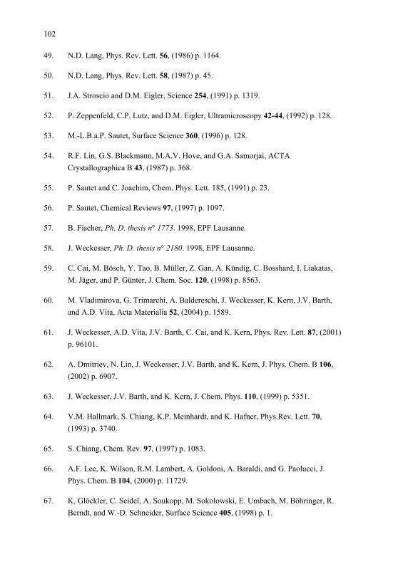
102
49. N.D. Lang, Phys. Rev. Lett. 56, (1986) p. 1164.
50. N.D. Lang, Phys. Rev. Lett. 58, (1987) p. 45.
51. J.A. Stroscio and D.M. Eigler, Science 254, (1991) p. 1319.
52. P. Zeppenfeld, C.P. Lutz, and D.M. Eigler, Ultramicroscopy 42-44, (1992) p. 128.
53. M.-L.B.a.P. Sautet, Surface Science 360, (1996) p. 128.
54. R.F. Lin, G.S. Blackmann, M.A.V. Hove, and G.A. Samorjai, ACTA Crystallographica B 43, (1987) p. 368.
55. P. Sautet and C. Joachim, Chem. Phys. Lett. 185, (1991) p. 23.
56. P. Sautet, Chemical Reviews 97, (1997) p. 1097.
57. B. Fischer, Ph. D. thesis n° 1773. 1998, EPF Lausanne.
58. J. Weckesser, Ph. D. thesis n° 2180. 1998, EPF Lausanne.
59. C. Cai, M. Bösch, Y. Tao, B. Müller, Z. Gan, A. Kündig, C. Bosshard, I. Liakatas, M. Jäger, and P. Günter, J. Chem. Soc. 120, (1998) p. 8563.
60. M. Vladimirova, G. Trimarchi, A. Baldereschi, J. Weckesser, K. Kern, J.V. Barth, and A.D. Vita, Acta Materialia 52, (2004) p. 1589.
61. J. Weckesser, A.D. Vita, J.V. Barth, C. Cai, and K. Kern, Phys. Rev. Lett. 87, (2001) p. 96101.
62. A. Dmitriev, N. Lin, J. Weckesser, J.V. Barth, and K. Kern, J. Phys. Chem. B 106,(2002) p. 6907.
63. J. Weckesser, J.V. Barth, and K. Kern, J. Chem. Phys. 110, (1999) p. 5351.
64. V.M. Hallmark, S. Chiang, K.P. Meinhardt, and K. Hafner, Phys.Rev. Lett. 70,(1993) p. 3740.
65. S. Chiang, Chem. Rev. 97, (1997) p. 1083.
66. A.F. Lee, K. Wilson, R.M. Lambert, A. Goldoni, A. Baraldi, and G. Paolucci, J. Phys. Chem. B 104, (2000) p. 11729.
67. K. Glöckler, C. Seidel, A. Soukopp, M. Sokolowski, E. Umbach, M. Böhringer, R. Berndt, and W.-D. Schneider, Surface Science 405, (1998) p. 1.
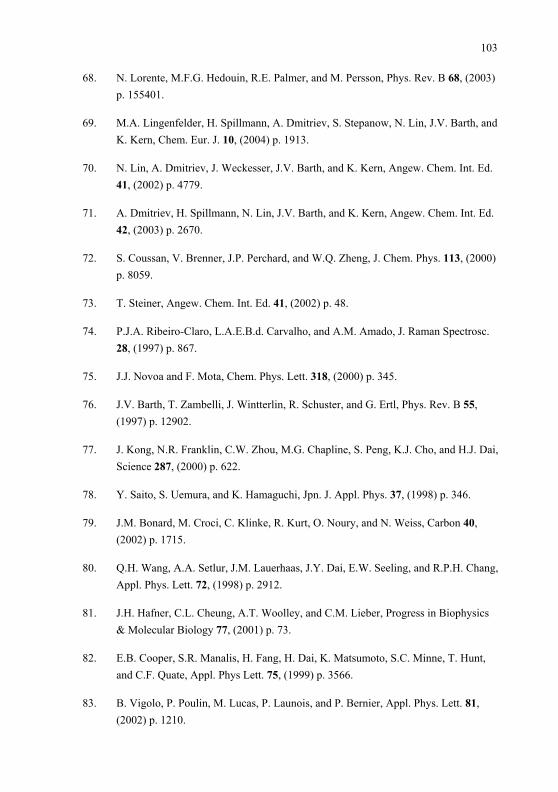
103
68. N. Lorente, M.F.G. Hedouin, R.E. Palmer, and M. Persson, Phys. Rev. B 68, (2003) p. 155401.
69. M.A. Lingenfelder, H. Spillmann, A. Dmitriev, S. Stepanow, N. Lin, J.V. Barth, and K. Kern, Chem. Eur. J. 10, (2004) p. 1913.
70. N. Lin, A. Dmitriev, J. Weckesser, J.V. Barth, and K. Kern, Angew. Chem. Int. Ed. 41, (2002) p. 4779.
71. A. Dmitriev, H. Spillmann, N. Lin, J.V. Barth, and K. Kern, Angew. Chem. Int. Ed. 42, (2003) p. 2670.
72. S. Coussan, V. Brenner, J.P. Perchard, and W.Q. Zheng, J. Chem. Phys. 113, (2000) p. 8059.
73. T. Steiner, Angew. Chem. Int. Ed. 41, (2002) p. 48.
74. P.J.A. Ribeiro-Claro, L.A.E.B.d. Carvalho, and A.M. Amado, J. Raman Spectrosc. 28, (1997) p. 867.
75. J.J. Novoa and F. Mota, Chem. Phys. Lett. 318, (2000) p. 345.
76. J.V. Barth, T. Zambelli, J. Wintterlin, R. Schuster, and G. Ertl, Phys. Rev. B 55,(1997) p. 12902.
77. J. Kong, N.R. Franklin, C.W. Zhou, M.G. Chapline, S. Peng, K.J. Cho, and H.J. Dai, Science 287, (2000) p. 622.
78. Y. Saito, S. Uemura, and K. Hamaguchi, Jpn. J. Appl. Phys. 37, (1998) p. 346.
79. J.M. Bonard, M. Croci, C. Klinke, R. Kurt, O. Noury, and N. Weiss, Carbon 40,(2002) p. 1715.
80. Q.H. Wang, A.A. Setlur, J.M. Lauerhaas, J.Y. Dai, E.W. Seeling, and R.P.H. Chang, Appl. Phys. Lett. 72, (1998) p. 2912.
81. J.H. Hafner, C.L. Cheung, A.T. Woolley, and C.M. Lieber, Progress in Biophysics & Molecular Biology 77, (2001) p. 73.
82. E.B. Cooper, S.R. Manalis, H. Fang, H. Dai, K. Matsumoto, S.C. Minne, T. Hunt, and C.F. Quate, Appl. Phys Lett. 75, (1999) p. 3566.
83. B. Vigolo, P. Poulin, M. Lucas, P. Launois, and P. Bernier, Appl. Phys. Lett. 81,(2002) p. 1210.
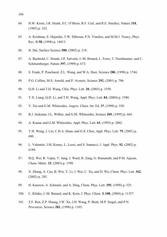
104
84. H.W. Kroto, J.R. Heath, S.C. O’Brien, R.F. Curl, and R.E. Smalley, Nature 318,(1985) p. 162.
85. A. Krishnan, E. Dujardin, T.W. Ebbesen, P.N. Yianilos, and M.M.J. Treacy, Phys. Rev. B 58, (1998) p. 14013.
86. H. Dai, Surface Science 500, (2002) p. 218.
87. A. Bachtold, C. Strunk, J.P. Salvetat, J.-M. Bonard, L. Forro, T. Nussbaumer, and C. Schönenberger, Nature 397, (1999) p. 673.
88. S. Frank, P. Poncharal, Z.L. Wang, and W.A. Heer, Science 280, (1998) p. 1744.
89. P.G. Collins, M.S. Arnold, and P. Avouris, Science 292, (2001) p. 706.
90. Q.H. Li and T.H. Wang, Chin. Phys. Lett. 20, (2003) p. 1558.
91. Y.X. Liang, Q.H. Li, and T.H. Wang, Appl. Phys. Lett. 84, (2004) p. 3380.
92. Y. Xia and G.M. Whitesides, Angew. Chem. Int. Ed. 37, (1998) p. 550.
93. R.J. Jackman, J.L. Wilbur, and G.M. Whitesides, Science 269, (1995) p. 664.
94. A. Kumar and G.M. Whitesides, Appl. Phys. Lett. 63, (1993) p. 2002.
95. Y.H. Wang, J. Lin, C.H.A. Huan, and G.S. Chen, Appl. Phys. Lett. 79, (2001) p. 680.
96. L. Valentini, J.M. Kenny, L. Lozzi, and S. Santucci, J. Appl. Phys. 92, (2002) p. 6188.
97. B.Q. Wei, R. Vajtai, Y. Jung, J. Ward, R. Zang, G. Ramanath, and P.M. Ajayan, Chem. Mater. 15, (2003) p. 1598.
98. X. Zhang, A. Cao, B. Wei, Y. Li, J. Wei, C. Xu, and D. Wu, Chem. Phys. Lett. 362,(2002) p. 285.
99. H. Kanzow, A. Schmalz, and A. Ding, Chem. Phys. Lett. 295, (1998) p. 525.
100. C. Klinke, J.-M. Bonard, and K. Kern, J. Phys. Chem. B 108, (2004) p. 11357.
101. Z.F. Ren, Z.P. Huang, J.W. Xu, J.H. Wang, P. Bush, M.P. Siegal, and P.N. Provencio, Science 282, (1998) p. 1105.
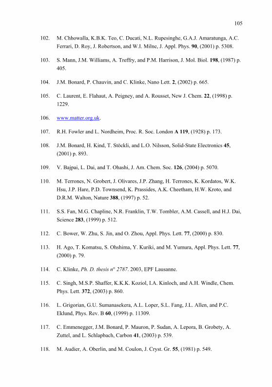
105
102. M. Chhowalla, K.B.K. Teo, C. Ducati, N.L. Rupesinghe, G.A.J. Amaratunga, A.C. Ferrari, D. Roy, J. Robertson, and W.I. Milne, J. Appl. Phys. 90, (2001) p. 5308.
103. S. Mann, J.M. Williams, A. Treffry, and P.M. Harrison, J. Mol. Biol. 198, (1987) p. 405.
104. J.M. Bonard, P. Chauvin, and C. Klinke, Nano Lett. 2, (2002) p. 665.
105. C. Laurent, E. Flahaut, A. Peigney, and A. Rousset, New J. Chem. 22, (1998) p. 1229.
106. www.matter.org.uk.
107. R.H. Fowler and L. Nordheim, Proc. R. Soc. London A 119, (1928) p. 173.
108. J.M. Bonard, H. Kind, T. Stöckli, and L.O. Nilsson, Solid-State Electronics 45,(2001) p. 893.
109. V. Bajpai, L. Dai, and T. Ohashi, J. Am. Chem. Soc. 126, (2004) p. 5070.
110. M. Terrones, N. Grobert, J. Olivares, J.P. Zhang, H. Terrones, K. Kordatos, W.K. Hsu, J.P. Hare, P.D. Townsend, K. Prassides, A.K. Cheetham, H.W. Kroto, and D.R.M. Walton, Nature 388, (1997) p. 52.
111. S.S. Fan, M.G. Chapline, N.R. Franklin, T.W. Tombler, A.M. Cassell, and H.J. Dai, Science 283, (1999) p. 512.
112. C. Bower, W. Zhu, S. Jin, and O. Zhou, Appl. Phys. Lett. 77, (2000) p. 830.
113. H. Ago, T. Komatsu, S. Ohshima, Y. Kuriki, and M. Yumura, Appl. Phys. Lett. 77,(2000) p. 79.
114. C. Klinke, Ph. D. thesis n° 2787. 2003, EPF Lausanne.
115. C. Singh, M.S.P. Shaffer, K.K.K. Koziol, I.A. Kinloch, and A.H. Windle, Chem. Phys. Lett. 372, (2003) p. 860.
116. L. Grigorian, G.U. Sumanasekera, A.L. Loper, S.L. Fang, J.L. Allen, and P.C. Eklund, Phys. Rev. B 60, (1999) p. 11309.
117. C. Emmenegger, J.M. Bonard, P. Mauron, P. Sudan, A. Lepora, B. Grobety, A. Zuttel, and L. Schlapbach, Carbon 41, (2003) p. 539.
118. M. Audier, A. Oberlin, and M. Coulon, J. Cryst. Gr. 55, (1981) p. 549.
106
119. D.B. Geohegan, A.A. Puretzky, I.N. Ivanov, S. Jesse, G. Eres, and J.Y. Howe, Appl. Phys. Lett. 83, (2003) p. 1851.
120. H.J. Yoon, H. S. Kang, J.S. Shin, J.S. Kim, K.J. Son, C.H. Lee, C.O. Kim, J.P. Hong, S.N. Cha, B.G. Song, J.M. Kim, and N.S. Lee, Physica B. 323, (2002) p. 344.
121. M. Liebau, E. Unger, G.S. Duesberg, A.P. Graham, R. Siedel, F. Kreupel, and W. Hoenlein, Appl. Phys. A 77, (2003) p. 731.
122. M. Burghard, V. Krstic, G.S. Duesberg, G. Philipp, J. Muster, S. Roth, C. Journet, and P. Bernier, Synth. Metals 103, (1999) p. 2540.
123. S. Banerjee and S. S.Wong, Nano Lett. 2, (2002) p. 195.
124. Y. Zhang, N.W. Franklin, R.J. Chen, and H. Dai, Chem. Phys. Lett. 331, (2000) p. 35.
125. M. Menon, A.N. Andriotis, and G.E. Froudakis, Chem. Phys. Lett. 320, (2000) p. 425.
126. X.P. Gao, Y. Zhang, X. Chen, G.L. Pan, J. Yan, F. Wu, H.T. Yuan, and D.Y. Song, Carbon 42, (2004) p. 47.
127. T.C. Rojas, M.J. Sayague, A. Caballero, Y. Koltypin, A. Gedanken, L. Ponsonnet, B. Vacher, J.M. Martin, and A. Fernandez, J. Mater. Chem. 10, (2000) p. 715.
128. P. Zhang, F. Zuo, F.K. Urban, A. Khabari, P. Griffiths, and A. Hosseini-Tehrani, Journal of Magnetism and Magnetic Materials 225, (2001) p. 337.
129. S.X. McFadden, A.P. Zhilyaev, R.S. Mishra, and A.K. Mukherjee, Materials Letters 45, (2000) p. 345.
130. D. Strzeciwilk, Z. Wokulski, and P. Tkacz, Cryst. Res. Technol. 38, (2003) p. 283.
131. W. Ostwald, Z. Phys. Chem. 34, (1900) p. 495.
132. Y. Fan, M. Burghard, and K. Kern, Adv. Mat. 14, (2002) p. 130.
133. L. Barfotti, P. Jensen, A. Hoareau, M. Treilleux, B. Cabaud, A. Perez, and F. Aires, Surf. Sci. 367, (1996) p. 276.
134. American Institute of Physics handbook. 3rd ed, ed. D.E. Gray. 1972, New York: McGraw-Hill Book Company.

107
135. L. Nilsson, O. Groening, C. Emmenegger, O. Kuettel, E. Schaller, L. Schlapbach, H. Kind, J.-M. Bonard, and K. Kern, Appl. Phys. Lett 76, (2000) p. 2071.
136. J.M. Bonard, N. Weiss, H. Kind, T. Stöckli, L. Forro, K. Kern, and A. Chatelain, Adv. Mater. 13, (2001) p. 184.

108

109
Acknowledgements
I would like to thank Prof. Peter Günter and Prof. Klaus Kern for giving me the opportunity to work in their groups in respectively Zürich and Lausanne.
The first part of my thesis work took place in Zürich where I want to thank my supervisor Ivan Biaggio for the discussions and for sharing his knowledge on nonlinear and linear optics with me. Axelle Tapponnier for the collaboration on the nonlinear optical thin films. Michael Kiy (my office mate) for teaching me how to work with the OMBD installation, for his great help improving my German knowledge and for letting me win once in table tennis.
Related to my time in Lausanne I like to thank my thesis director Johannes Barth for his input in many parts of my thesis work. Christian Klinke for introducing me to the field of catalytic growth of carbon nanotubes, for the cooperation and discussions in this field and for the fun Wednesday-night tours from Bleu Lézard via Captain Cook to the Jagger’s. Sylvain Clair, my other long-term office mate, who helped me with a great deal of questions ranging from physics problems to questions about the French language. My further office mates Agustin Schiffrin and Marta Cañas Ventura who, as Spanish speaking people, suffered the most under my attempts to speak Spanish on Tuesdays. I want to thank all of them for the good atmosphere in the office. Furthermore I want to thank Stéphane Pons, the post-doc in our group, for the enthusiasm with which he filled the blackboard in our office with research ideas, illustrated discussions and “physi-chien” drawings.
In Stuttgart I like to thank Franck Vidal with whom I made the STM measurements and discussed the results, continuing even after I had returned to Lausanne. Furthermore I like to thank Nian Lin, Sebastian Stepanow, Sacha Dmitriev and Hannes Spillmann for their help with the STM and the measurements and for the discussions. Special thanks goes to Magali Lingenfelder and Diego Repetto for taking me to the University for lunch many times, in this way escaping the experiments of MPI’s English cook.
There is a also a great number of other people in the institutes in Zürich, Lausanne and Stuttgart, who I didn’t mention above, but to whom I am very grateful for their technical

110
support, administrative support, discussions, their company during coffee breaks and lunch breaks, conversations, jokes, small talk, big talk …….. The list of names of all those people would get too long to write them all down here, but I hope that all those people that made working in the three groups to a pleasant experience know that they are the people in question here.
Last, but certainly not least, I want to thank my family and friends in the Netherlands who supported me on a long distance and/or came to visit me during my stay in Zürich and Lausanne and also the many new friends that I met over the last four years who made my stay here in Switzerland to such a great time.
111
Curriculum Vitae
Name: Erik Henri Adriaan Delvigne
Date of Birth: 25 July 1975
Nationality: Dutch
1987 – 1993 High School at the Oranje Nassau College in Zoetermeer, The Netherlands.
1993 – 1998 Studies in applied physics at the Delft University of Technology, The Netherlands.
Sept. – Dec. 1997 Traineeship in the group of Prof. P. Renaud at the Microtechnics Institute of the Swiss Federal Institute of Technology Lausanne, Switzerland.
1998 Diploma thesis in the group of Prof. J.E. Mooij at the Delft University of Technology, The Netherlands: “Subgap Tunneling in a Superconducting Single Electron Tunneling Transistor”.
1999 – 2000 Analyst in the Technology group of Andersen Consulting, Amsterdam, The Netherlands.
2000 – 2004 Research and teaching assistant in the group of Prof. P. Günter at the Institute for Experimental Physics of the Swiss Federal Institute of Technology Zürich and the group of Prof. K. Kern at Institute for Experimental Physics of the Swiss Federal Institute of Technology Lausanne, Switzerland.
December 2004 Ph.D. Thesis, EPFL, Lausanne, Switzerland.

112