Embed Size (px)
Citation preview

Energy-Efficient Processor Design Using Multiple Clock Domains with Dynamic Voltage and Frequency Scaling*
Greg Semeraro, Grigorios Magklis, Rajeev Balasubramonian, David H. Albonesi, Sandhya Dwarkadas, and Michael L. Scott
Departments of Computer Science and of Electrical and Computer Engineering University of Rochester
{ semeraro, albonesi}@ece.rochester.edu {maglis, rajeev, sandhya, scott}@cs.rochester.edu
Abstract
As clock frequency increases and feature size decreases, clock distribution and wire delays present a growing chal- lenge to the designers of singly-clocked, globally syn- chronous systems. We describe an alternative approach, which we call a Multiple Clock Domain (MCD) processon in which the chip is divided into several (coarse-grained) clock domains, within which independent voltage and fre- quency scaling can be per$ormed. Boundaries between do- mains are chosen to exploit existing queues, thereby min- imizing inter-domain synchronization costs. We propose four clock domains, corresponding to the front end (in- cluding LI instruction cache), integer units, floating point units, and load-store units (including Ll data cache and L2 cache). We evaluate this design using a simulation infras- tructure based on SimpleScalar and Wattch. In an attempt to quantify potential energy savings independent of any particular on-line control strategy, we use of-line analysis of traces from a single-speed run of each of our benchmark applications to identify profitable reconfiguration points for a subsequent dynamic scaling run. Dynamic runs in- corporate a detailed model of inter-domain synchroniza- tion delays, with latencies for intra-domain scaling simi- lar to the whole-chip scaling latencies of Intel XScale and Transmeta LongRun technologies. Using applications from the MediaBench, Olden, and SPEC2000 benchmark suites, we obtain an average energy-delay product improvement of 20% with MCD compared to a modest 3% savings from voltage scaling a single clock and voltage system.
*This work was supported in part by NSF grants CCR-9701915, CCR-9702466, CCR-9705594, CCR-9811929, EM-9972881, CCR- 9988361, and EIA-0080124; by DARPMTO under AFRL con- tract F2%01-00-K-0182; and by an external research grant from DECYCompaq.
1. Introduction
The continuing push for higher microprocessor perfor- mance has led to unprecedented increases in clock frequen- cies in recent years. While the Pentium III microprocessor broke the 1GHz barrier in 2000, the Pentium IV is currently shipping at 2GHz. At the same time, due to issues of relia- bility and performance, wire dimensions have been scaled in successive process generations more conservatively than transistor dimensions. The result of these frequency and di- mensional trends is that microprocessor clock speeds have become increasingly limited by wire delays, so much so that some of the more recent microprocessors, e.g., the Pen- tium IV [ 141, have pipeline stages solely dedicated to mov- ing signals across the chip. Furthermore, a growing chal- lenge in future systems will be to distribute the clock across a progressively larger die to increasing numbers of latches while meeting a decreasing clock skew budget. The in- evitable conclusion reached by industrial researchers is that in order to continue the current pace of clock frequency in- creases, microprocessor designers will eventually be forced to abandon singly-clocked globally synchronous systems in favor of some form of asynchrony [S, 241.
Although purely asynchronous systems have the poten- tial for higher performance and lower power compared to their synchronous counterparts, major corporations have been reluctant to fully migrate to asynchronous design methodologies. Two major reasons for this reluctance are the immaturity of asynchronous design tools relative to those in the synchronous domain, and the cost and risk of moving away from the mature design infrastructures that have been successfully used to create many generations of microprocessor products. Yet many existing synchronous designs do incorporate a limited amount of asynchrony. For example, several multiprocessor systems run the memory bus off of a different clock than the processor core in or-
Proceedings of the Eighth International Symposium on High-Performance Computer Architecture (HPCA�02) 1503-0897/02 $17.00 © 2002 IEEE

der to allow a single system to accommodate processors of different frequencies. In such dual clock domain systems, the logic in each of the two clock domains is designed us- ing conventional synchronous design methodologies. Well- known and highly-reliable techniques are used to synchro- nize communication between the two domains, albeit at the cost of extra delay.
An additional trend due to the wire scaling dilemma is to replace microarchitectural techniques requiring long global wires with alternatives requiring only local wiring. This approach improves both clock frequency and the scalabil- ity of the design in future process generations. For exam- ple, in several microprocessors including the Alpha 21164 and 21264 [ll, 201 and the UltraSPARC III [17], the use of global wires to stall early pipeline stages has been re- placed by the use of replay traps that cancel instructions and restart the pipeline. Although flushing the pipeline in this manner requires additional cycles for reloading, it re- sults in a higher clock frequency and more scalable imple- mentation due to the elimination of global wires. The de- signers of the UltraSPARC III fully embraced this approach by creating six functional blocks that run relatively inde- pendently of one another, with most long wires eliminated between units [ 171.
An approach that allows for aggressive future frequency increases, maintains a synchronous design methodology, and exploits the trend towards making functional blocks more autonomous, is a multiple clock domain (MCD) microarchitecture, which uses a globally-asynchronous, locally-synchronous (GALS) clocking style. In an MCD microprocessor each functional block operates with a sepa- rately generated clock, and synchronizing circuits ensure reliable inter-domain communication. Thus, fully syn- chronous design practices are used in the design of each domain. Although the inter-domain synchronization in- creases the number of clock cycles required to run a given application, an MCD microprocessor affords a number of potential advantages over a singly clocked design:
l The global clock distribution network is greatly sim- plified, requiring only the distribution of the externally generated clock to the local Phase Lock Loop (PLL) in each domain. The independence of each local do- main clock implies no global clock skew requirement, permitting potentially higher frequencies within each domain and greater scalability in future process gen- erations.
l The designers of each domain are no longer con- strained by the speeds of critical paths in other do- mains, affording them greater freedom in each do- main to optimize the tradeoffs among clock speed, la- tency, and the exploitation of application parallelism via complex hardware structures.
Using separate voltage inputs, external voltage regula- tors, and controllable clock frequency circuits in each clock domain allows for finer grained dynamic volt- age and frequency scaling, and thus lower energy, than can be achieved with single clock, single-core-voltage systems.
With the ability to dynamically resize structures and alter the clock speed in each domain, the IPC/clock rate tradeoff can be tailored to application character- istics within each individual domain [l], thereby im- proving both performance and energy efficiency.
In this paper, we describe an initial implementation of an MCD microprocessor that is a straightforward exten- sion of a singly-clocked synchronous dynamic superscalar design. By accurately modeling inter-domain synchroniza- tion, we characterize the performance and energy costs of the required synchronization circuitry. We then explore the potential benefits of per-domain dynamic voltage and fre- quency scaling. Our results demonstrate a 20% average im- provement in energy-delay product for a set of benchmarks that includes both compute and memory-bound applica- tions. Unlike rate-based multimedia applications, these benchmarks have not traditionally been candidates for volt- age and frequency scaling.
The rest of the paper is organized as follows. In Sec- tion 2, we describe a microarchitecture with four separate clock domains, comprising the front end (including Ll in- struction cache, rename, and reorder buffer), integer unit, floating-point unit, and load-store unit (including Ll data cache and L2 cache). We discuss the circuitry needed for cross-domain synchronization, and its performance costs. In Section 3, we describe the simulation infrastructure we used to evaluate this microarchitecture. The simulator, based on SimpleScalar and Wattch, includes detailed mod- eling of synchronization costs. We also describe an off-line analysis tool that we used in our experiments to identify promising points at which to reconfigure (scale) domains in various applications. Our performance and energy dissipa- tion results, reported in Section 4, encompass applications from the MediaBench, Olden, and SPEC 2000 benchmark suites. Sections 5 and 6 contain additional discussion of related work and concluding remarks.
2. Multiple Clock Domain Microarchitecture
2.1. Division of Chip into Clock Domains Matzke has estimated that as technology scales down to
a O.lpum feature size, only 16% of the die will be reachable within a single clock cycle [24]. Assuming a chip multipro- cessor with two processors per die, each processor would need to have a minimum of three equal-size clock domains. Our design uses four domains, one of which includes the
Proceedings of the Eighth International Symposium on High-Performance Computer Architecture (HPCA�02) 1503-0897/02 $17.00 © 2002 IEEE

L2 cache, so that domains may vary somewhat in size and still be covered by a single clock. In effect, we treat the main memory interface as a fifth clock domain, external to the MCD processor, and always running at full speed.
In choosing the boundaries between domains, we at- tempted to identify points where (a) there already ex- isted a queue structure that served to decouple differ- ent pipeline functions, or (b) there was relatively little inter-function communication. Our four chosen domains, shown in Figure 1, comprise the front end (including in- struction cache, branch prediction, rename, and dispatch); integer issue/execute; floating point issue/execute; and load/store issue/execute. Although we were initially con- cerned about the performance impact of implementing sep- arate load/store and integer domains, we discovered that the additional synchronization penalty did not significantly degrade performance. Furthermore, because we discovered no energy savings from decoupling instruction fetch from rename/dispatch, we combined these regions into a sin- gle fetch/rename/dispatch domain to eliminate their inter- domain synchronization overhead. Finally, execution units of the same type (e.g., integer units) were combined into a single domain to avoid the high cost of synchronizing the bypass and register file datapaths among these units. As a result of these divisions, there were no explicit changes to the pipeline organization of the machine. We also believe that these divisions would result in a physically realizable floorplan for an MCD processor.
n m
Figure 1. Multiple clock domain processor block diagram
2.2. Inter-Domain Synchronization
The primary disadvantage of an MCD processor is the performance overhead due to inter-domain synchroniza- tion. In this section, we discuss the circuitry required to perform this synchronization. We discuss how to model its performance cost in Section 4.
Some synchronization schemes restrict the phase rela- tionship and relative frequencies of the clocks, thereby eliminating the need for hardware arbitration [27]. Un- fortunately, these schemes impose significant restrictions on the possible choices of frequencies. In addition, the need to control the phase relationships of the clocks means that global clock synchronization is required. Our design specifically recognizes the overhead associated with inde- pendent clocks with no known phase relationship. We be- lieve this overhead to be unavoidable in an MCD processor: one of the motivating factors for the design is the recogni- tion that traditional global clock distribution will become increasingly difficult in the future.
The issue queues in the integer, floating point, and load/store domains (the Load/Store Queue within the Load/Store Unit), together with the Reorder Buffer (ROB) in the front end domain, serve to decouple the front and back ends of a conventional processor. Choosing these queues as inter-domain synchronization points has the ad- vantage of hiding the synchronization cost whenever the queue is neither full nor empty (as described later in this section).
CLOCK(w) QUEUE CLOCK(r)
WRITE READ
DATA(w) DATA(r)
FULL
_
EMPTY
Figure 2. Queue structure
The general queue structure that we use for inter-domain communication is shown in Figure 2. The assertion of the Full flag indicates to the producer that it can no longer write to the queue until the flag is deasserted (Full), while the Empty flag when asserted indicates that there is no valid data for the consumer to read from the queue. The consumer waits until Empty is deasserted before reading again.
The use of a full handshake protocol for this interface re- quires that the producer/consumer check the Full/Empty flag after every operation in order to avoid queue overruns on writes or reads from an empty queue. This requirement significantly slows down the interface thereby degrading performance. Rather, we assume that the FUZZ and Empty flags are generated far enough in advance such that writes and reads can occur every clock cycle without over or un- derflowing the queue. In other words, the FUZZ flag is gen- erated early enough such that a burst of writes every cycle will terminate (due to recognition by the producer of the a+ sertion of the FUZZ flag) just as the last remaining queue en- try has been written. An analogous situation exists for the consumer side of the queue, although our particular queues are different in this regard as we discuss later. Note that this scheme may result in underutilization of the queue under
Proceedings of the Eighth International Symposium on High-Performance Computer Architecture (HPCA�02) 1503-0897/02 $17.00 © 2002 IEEE

particular conditions. For example, if the write that initi- ates assertion of the Full flag is at the end of a burst, then there will be empty but unusable entries in the queue (be- cause the Full flag will have been asserted) the next time the producer has data to write into the queue.
In order to avoid underutilization of the queues, we as- sume extra queue entries to buffer writes under worst-case conditions so that the original number of queue entries can be fully utilized. In the MCD design, the worst-case sit- uation occurs when the producer is operating at the maxi- mum frequency (ma%-freq) and the consumer at the min- imum (min-freq). An additional complication occurs due to the need to compare queue head and tail pointers from different clock domains in order to generate the Full and Empty flags. Under these conditions, and assuming an ad- ditional cycle for the producer to recognize the FUZZ signal, (maa:-freq/min-freq) + 1 additional entries are required. Note that our results do not account for the performance ad- vantage nor the energy cost of these additional entries.
Even with completely independent clocks for each in- terface, the queue structure is able to operate at full speed for both reading and writing under certain conditions. This concurrency requires a dual-ported SRAM structure where simultaneous read and write cycles are allowed to diflerent SRAM cells. As long as the interfaces are designed to ad- here to the protocol associated with the FUZZ and Empty flags, the queue structure does not need to support simul- taneous read and write access to the same SRAM cell. As long as the queue is not full (as described above) the pro- ducer can continue to write data on every rising edge of CZockw (Figure 3). Similarly, so long as the queue is not empty, the consumer can continue reading on every rising edge of Clock,. Therefore, both interfaces operate at full speed so long as the queue is partially full, although newly written entries may not be recognized by the consumer un- til after a synchronization period. Once the queue becomes full, the queue state of FUZZ can only result from data being read out of the queue on the read interface. When this event occurs, the queue pointer in the read domain must get syn- chronized with the write domain clock (CZocie,) in order to deassert FUZZ. A similar synchronization delay occurs with the generation of the Empty condition due to a write to an empty queue.
Many of the queues that we use as synchronization points have a different interface than that described above. For the issue queue for example, each entry has Valid and Ready flags that the scheduler uses to determine if an entry should be read (issued). The scheduler by design will never issue more than the number of valid and ready entries in the queue. Note, however, that due to synchronization, there is a delay before the scheduler sees newly written queue data.
The delay associated with crossing a clock domain in- terface is a function of the following:
CLOCK(w) m
WRITE 2 um STALLED
DATA(w) -----+ H - N-7 :rc, N
FULL ‘3
Figure 3. Full flag
l The synchronization time of the clock arbitration cir- cuit, Ts, which represents the minimum time required between the source and destination clocks in order for the signal to be successfully latched at the destina- tion. We assume the arbitration and synchronization circuits developed by Sjogren and Myers [28] that de- tect whether the source and destination clock edges are sufficiently far apart (at minimum, Ts) such that a source-generated signal can be successfully clocked at the destination. The destination clock is enabled only under these conditions. We assume a Z’S of 30% of the period of the highest frequency.
l The ratio of the frequencies of the interface clocks.
l The relative phases of the interface clocks.
This delay can best be understood by examining a tim- ing diagram (Figure 4), which shows source clock Fl and destination clock Fz. Consider the case when the queue
FI- F2-lAlJ-L
Y Figure 4. Synchronization timing
is initially empty. Data is written into the queue on the rising edge of FI (edge 1). Data can be read out of the queue as early as the next rising edge of Fz (edge 2), if and only if 2’ > Z’S, i.e., Empty has become false on the Fz interface before the next rising edge of Fz. If T 5 Ts, the earliest that the data can be read is one Fz period later (edge 3). This extra delay represents one source of perfor- mance degradation due to synchronization. The value of T is determined by the relative frequency and phases of FI and Fz, as well as the relative jitter of the clock sources, and may change over time. The cost of synchronization is controlled by the relationship between 2’ and Z’S, and to a lesser degree by the magnitude of Ts. The analogous situa- tion exists when the queue is Full, replacing Empty with Full, edge 1 with edge 2, and edge 3 with edge 4 in the above discussion.
In our simulator, described in the next section, we accu- rately account for inter-domain overhead.
Proceedings of the Eighth International Symposium on High-Performance Computer Architecture (HPCA�02) 1503-0897/02 $17.00 © 2002 IEEE
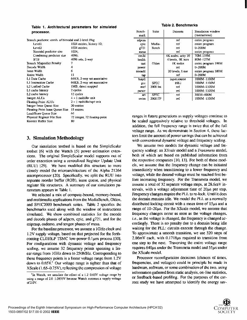
Table 1. Architectural parameters for simulated processor.
Branch predictor: comb. of bimodal and 2-level PAg Level1 1024 entries, history 10; Level2 1024 entries; Bimodal predictor size 1024; Combining predictor size 4096; BIB 4096 sets, 2-way
Branch Mispredict Penalty 7 Decode Width 4 Issue Width 6 Retire Width 11 Ll Data Cache &lKB, 2-way set associative Ll Instruction Cache 64KB, 2-way set associative L2 Unified Cache lMB, direct mapped Ll cache latency 2 cycles L2 cache latency 12 cycles Integer ALUs 4 + 1 muh/div unit Floating-Point ALUs 2 + 1 mult/div/sqrt unit Integer Issue Queue Size 20 entries Floating-Point Issue Queue Size 15 entries Load/Store Queue Size 64 Physical Register File Size 72 integer, 72 floating-point Reorder Buffer Size 80
3. Simulation Methodology
Our simulation testbed is based on the SimpleScalar toolset [6] with the Wattch [5] power estimation exten- sions. The original SimpleScalar model supports out of order execution using a centralized Register Update Unit (RUU) [29]. We have modified this structure to more closely model the microarchitecture of the Alpha 21264 microprocessor [20]. Specifically, we split the RUU into separate reorder buffer (ROB), issue queue, and physical register file structures. A summary of our simulation pa- rameters appears in Table 1.
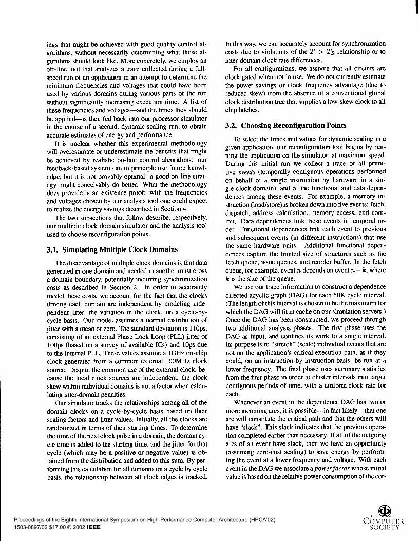
We selected a mix of compute-bound, memory-bound, and multimedia applications from the MediaBench, Olden, and SPEC2000 benchmark suites. Table 2 specifies the benchmarks used along with the window of instructions simulated. We show combined statistics for the encode and decode phases of adpcm, epic, and g721, and for the mipmap, osdemo, and texgen phases of mesa.
For the baseline processor, we assume a 1GHz clock and 1.2V supply voltage, based on that projected for the forth- coming CLOlOLP TSMC low-power O.lpm process [30]. For configurations with dynamic voltage and frequency scaling, we assume 32 frequency points spanning a lin- ear range from 1GHz down to 250MHz. Corresponding to these frequency points is a linear voltage range from 1.2V down to 0.65V.l Our voltage range is tighter than that of XScale (1.65-0.75V), reflecting the compression of voltage
‘In Wattch, we simulate the effect of a 1.2-0.65V voltage range by using a range of 2.&1.0833V because Wattch assumes a supply voltage of 2.OV
Bench- mark
adpcm epic
g721 mesa em3d health
mst POW”
treeadd t sP
bzip2 w mcf
art swim
Suite
Table 2. Benchmarks
Media- Bench
Olden
SPEC 2000 Int
SPEC 2000 FP
Datasets
ref ref ref ref
4K nodes, arity 10 4 levels, 1K iters
1K nodes ref
20 levels, 1 iter ref
input.source lti.i ref ref ref ref
Simulation window (instructions)
entire program entire program &2OOM entire program 7OM-119M 8OM-127M entire program 199M &2OOM entire program 189M 0-2oOM 1 OOOM-1lOOM 1 OOOM-1 1OOM 1 OOOM-1 1OOM 1 OOOM-1 1OOM 300M#OM lOOOM-11OOM
ranges in future generations as supply voltages continue to be scaled aggressively relative to threshold voltages. In addition, the full frequency range is twice that of the full voltage range. As we demonstrate in Section 4, these fac- tors limit the amount of power savings that can be achieved with conventional dynamic voltage and frequency scaling.
We assume two models for dynamic voltage and fre- quency scaling: an XScale model and a Transmeta model, both of which are based on published information from the respective companies [lo, 131. For both of these mod- els, we assume that the frequency change can be initiated immediately when transitioning to a lower frequency and voltage, while the desired voltage must be reached first be- fore increasing frequency. For the Transmeta model, we assume a total of 32 separate voltage steps, at 286mV in- tervals, with a voltage adjustment time of 20~s per step. Frequency changes require the PLL to re-lock. Until it does the domain remains idle. We model the PLL as a normally distributed locking circuit with a mean time of 15~s and a range of 10-20~s. For the XScale model, we assume that frequency changes occur as soon as the voltage changes, i.e., as the voltage is changed, the frequency is changed ac- cordingly. There is no penalty due to a domain being idle waiting for the PLL: circuits execute through the change. To approximate a smooth transition, we use 320 steps of 2.86mV each, with 0.1718~s required to transition from one step to the next. Traversing the entire voltage range requires 640~s under the Transmeta model and 55~s under the XScale model.
Processor reconfiguration decisions (choices of times, frequencies, and voltages) could in principle be made in hardware, software, or some combination of the two, using information gathered from static analysis, on-line statistics, or feedback-based profiling. For the purposes of the cur- rent study we have attempted to identify the energy sav-
Proceedings of the Eighth International Symposium on High-Performance Computer Architecture (HPCA�02) 1503-0897/02 $17.00 © 2002 IEEE
ings that might be achieved with good quality control al- gorithms, without necessarily determining what those al- gorithms should look like. More concretely, we employ an off-line tool that analyzes a trace collected during a full- speed run of an application in an attempt to determine the minimum frequencies and voltages that could have been used by various domains during various parts of the run without significantly increasing execution time. A list of these frequencies and voltages-and the times they should be applied-is then fed back into our processor simulator in the course of a second, dynamic scaling run, to obtain accurate estimates of energy and performance.
It is unclear whether this experimental methodology will overestimate or underestimate the benefits that might be achieved by realistic on-line control algorithms: our feedback-based system can in principle use future knowl- edge, but it is not provably optimal: a good on-line strat- egy might conceivably do better. What the methodology does provide is an existence proof: with the frequencies and voltages chosen by our analysis tool one could expect to realize the energy savings described in Section 4.
The two subsections that follow describe, respectively, our multiple clock domain simulator and the analysis tool used to choose reconfiguration points.
3.1. Simulating Multiple Clock Domains
The disadvantage of multiple clock domains is that data generated in one domain and needed in another must cross a domain boundary, potentially incurring synchronization costs as described in Section 2. In order to accurately model these costs, we account for the fact that the clocks driving each domain are independent by modeling inde- pendent jitter, the variation in the clock, on a cycle-by- cycle basis. Our model assumes a normal distribution of jitter with a mean of zero. The standard deviation is 1 lops, consisting of an external Phase Lock Loop (PLL) jitter of loops (based on a survey of available ICs) and lops due to the internal PLL. These values assume a 1GHz on-chip clock generated from a common external 1OOMHz clock source. Despite the common use of the external clock, be- cause the local clock sources are independent, the clock skew within individual domains is not a factor when calcu- lating inter-domain penalties.
Our simulator tracks the relationships among all of the domain clocks on a cycle-by-cycle basis based on their scaling factors and jitter values. Initially, all the clocks are randomized in terms of their starting times. To determine the time of the next clock pulse in a domain, the domain cy- cle time is added to the starting time, and the jitter for that cycle (which may be a positive or negative value) is ob- tained from the distribution and added to this sum. By per- forming this calculation for all domains on a cycle by cycle basis, the relationship between all clock edges is tracked.
In this way, we can accurately account for synchronization costs due to violations of the T > TS relationship or to inter-domain clock rate differences.
For all configurations, we assume that all circuits are clock gated when not in use. We do not currently estimate the power savings or clock frequency advantage (due to reduced skew) from the absence of a conventional global clock distribution tree that supplies a low-skew clock to all chip latches.
3.2. Choosing Reconfiguration Points
To select the times and values for dynamic scaling in a given application, our reconfiguration tool begins by run- ning the application on the simulator, at maximum speed. During this initial run we collect a trace of all primi- tive events (temporally contiguous operations performed on behalf of a single instruction by hardware in a sin- gle clock domain), and of the functional and data depen- dences among these events. For example, a memory in- struction (load/store) is broken down into five events: fetch, dispatch, address calculation, memory access, and com- mit. Data dependences link these events in temporal or- der. Functional dependences link each event to previous and subsequent events (in different instructions) that use the same hardware units. Additional functional depen- dences capture the limited size of structures such as the fetch queue, issue queues, and reorder buffer. In the fetch queue, for example, event n depends on event n - k, where k is the size of the queue.
We use our trace information to construct a dependence directed acyclic graph (DAG) for each 50K cycle interval. (The length of this interval is chosen to be the maximum for which the DAG will fit in cache on our simulation servers.) Once the DAG has been constructed, we proceed through two additional analysis phases. The first phase uses the DAG as input, and confines its work to a single interval. Its purpose is to “stretch” (scale) individual events that are not on the application’s critical execution path, as if they could, on an instruction-by-instruction basis, be run at a lower frequency. The final phase uses summary statistics from the first phase in order to cluster intervals into larger contiguous periods of time, with a uniform clock rate for each.
Whenever an event in the dependence DAG has two or more incoming arcs, it is possible-in fact likely-that one arc will constitute the critical path and that the others will have “slack”. This slack indicates that the previous opera- tion completed earlier than necessary. If all of the outgoing arcs of an event have slack, then we have an opportunity (assuming zero-cost scaling) to save energy by perform- ing the event at a lower frequency and voltage. With each event in the DAG we associate apowerfactor whose initial value is based on the relative power consumption of the cor-
Proceedings of the Eighth International Symposium on High-Performance Computer Architecture (HPCA�02) 1503-0897/02 $17.00 © 2002 IEEE

responding clock domain, as determined by parameters in Wattch. When we stretch an event we scale its power factor accordingly. Calculations are made on a relative basis, on the assumption that energy is proportional to the square of the clock frequency.
The stretching phase of our reconfiguration tool uses a “shaker” algorithm to distribute slack and scale edges as uniformly as possible. Since SimpleScalar, like any real processor, executes events as soon as possible subject to dependences and hazards, slack always appears at the ends of non-critical paths in the original execution trace. The shaker algorithm thus begins at the end of its 50K cycle in- terval and works backwards through the DAG. When it en- counters an event whose outgoing edges all have slack, the shaker checks to see whether the power factor of the event exceeds a certain threshold, originally set to be slightly be- low the maximum power of any event in the graph. If so (this is a high-power event), the shaker scales the event un- til either it consumes all the available slack or its power factor drops below the current threshold. If any slack re- mains, the event is moved later in time, so that as much slack as possible is moved to its incoming edges.
When it reaches the beginning of the DAG, the shaker reverses direction, reduces its power threshold by a small amount, and makes a new pass forward through the DAG, scaling high-power events and moving slack to outgoing edges. It repeats this process, alternately passing forward and backward over the DAG, reducing its power threshold each time, until all available slack has been consumed, or until all events adjacent to slack edges have been scaled down to one quarter of their original frequency. When it completes its work for a given 50K cycle interval, the shaker constructs a summary histogram for each clock do- main. Each histogram indicates, for each of the 320 fre- quency steps in the XScale model (being the maximum of the number of steps for the two models), the total number of cycles for the events in the domain and interval that have been scaled to run at or near that frequency.
Unfortunately, it turns out to be difficult to capture the behavior of the front end in terms of dependences among events. Unlike the time between, say, the beginning and the end of an add in the floating-point domain, the time be- tween fetch and dispatch is not a constant number of cycles. In addition, experiments with manually selected reconfigu- ration points suggested that scaling of the front was seldom as beneficial as scaling of other domains. As a result, we have chosen to run the front at a steady lGHz, and to apply the shaker algorithm to events in the other 3 domains only. Since the front end typically accounts for 20% of the total chip energy, this choice implies that any energy improve- ments we may obtain must come from the remaining 80%. Future attempts to address the front end may yield greater savings than are reported here.
The final, clustering phase of our off-line analysis tool recognizes that frequencies cannot change on an instanta- neous, instruction-by-instruction basis. It also allows for a certain amount of performance degradation. Using the histograms generated by the shaker, we calculate, for each clock domain and interval, the minimum frequency f that would permit the domain to complete its work with no more than d percent time dilation, where d is a parameter to the analysis. More specifically, we choose a frequency (from among 32 possible values for Transmeta and from among 320 possible values for XScale) such that the sum, over all events in higher bins of the histogram, of the ex- tra time required to execute those events at the chosen fre- quency is less than or equal to d percent of the length of the interval. This calculation is by necessity approximate. It ignores ILP within domains: it assumes that the dilations of separate events in the same domain will have a cumula- tive effect. At the same time it ignores most dependences across domains: it assumes that the dilations of events in different domains will be independent.2 For most appli- cations the overall time dilation estimate turns out to be reasonably accurate: the figures in Section 4 show perfor- mance degradation (with respect to the MCD baseline) that is roughly in keeping with d.
Whereas the shaker algorithm assumes that reconfigu- ration is instantaneous and free, the clustering algorithm must model reconfiguration times and costs. For each ad- jacent pair of intervals for a given domain, it merges his- tograms on a bin-by-bin basis and calculates the minimum frequency that would allow us to run the larger, combined interval at a single frequency. For the Transmeta power model we require that the time dilation of too-slow events together with the time required to reconfigure at interval boundaries not exceed d percent of total execution time. Since it eliminates one reconfiguration, merging intervals under the Transmeta model often allows us to run the com- bined interval at a lower frequency and voltage, thereby saving energy. Most mergers under the XScale model oc- cur when adjacent intervals have identical or nearly identi- cal target frequencies. The clustering algorithm continues to perform mergers, recursively, so long as it is profitable from an energy standpoint to do so.
When it is done performing mergers, the clustering al- gorithm calculates the times at which reconfiguration must begin in order to reach target frequencies and voltages at target times. If reconfiguration is not possible, for exam- ple, because of a large swing in frequency that would take longer (because of the time to reduce or increase voltage) than the available interval, it is avoided. Since transitions
2As an exception to this rule, we add the events of the load/store do- main into the histogram of the integer domain. This special case ensures that effective address computations occur quickly when memory activity is high.
Proceedings of the Eighth International Symposium on High-Performance Computer Architecture (HPCA�02) 1503-0897/02 $17.00 © 2002 IEEE

in the Transmeta model take 20~s per voltage level, this results in the inability to accommodate short intervals with a large frequency variance. The algorithm completes its work by writing a log file that specifies times at which the application could profitably have requested changes in the frequencies and voltages of various domains. This file is then read by the processor simulator during a second, dy- namic configuration run.
4. Results In this section, we compare the performance, energy,
and energy-delay product of the MCD microarchitecture to that of a conventional singly clocked system. The base- line configuration is a single clock 1GHz Alpha 21264- like system with no dynamic voltage or frequency scal- ing. The baseline MCD configuration is split into four clock domains as described in Section 2 but with the fre- quency of all clocks statically set at 1GHz. This configu- ration serves to quantify the performance and energy cost of inter-domain synchronization. The dynamic 1% and dy- namic 5% configurations are identical to baseline MCD ex- cept that they support dynamic voltage and frequency scal- ing within each clock domain, as described in Section 3. For the dynamic I% case the clustering phase of our off- line reconfiguration tool (Section 3.2) uses a target of 1% performance degradation (beyond that of baseline MCD); for the dynamic 5% case it uses a target of 5%. Finally, the global configuration models the baseline configuration with the addition of dynamic scaling of its single voltage and frequency, and serves to quantify the benefits of multi- ple clock domains.
The frequency for the global case is set so as to incur an overall performance degradation equal to that of the dy- namic 5% configuration, and its voltage is correspondingly reduced. The energy savings of global is calculated by running each application under SimpleScalar and Wattch using the reduced frequency and voltage values. This ap- proach permits the energy savings of the MCD approach to be compared to that of conventional voltage and frequency scaling for the same level of performance degradation. We performed a sanity check of the energy results of the global configuration by comparing the Wattch results against a simple calculation of the energy of the baseline configu- ration scaled relative to the square of the voltage ratios and found the results to agree to within 2%.
Figures 5,6, and 7 display the performance degradation, energy savings, and change in energy x delay of the base- line MCD, dynamic I%, dynamic 5%, and global config- urations with respect to the baseline configuration, under the XScale model of voltage and frequency scaling. The Transmeta model produced far less promising results than the XScale model. Because of the roughly 15~~s required to re-lock the PLL under the Transmeta model, rcconfigu-
1 8 96
1 6 %
14%
12%
10%
6%
6%
4%
2%
0 36
ii ri 5 ‘0 m
~ i E f E
b m
10 Baseline MCD [II Dynamic-l q Dynamic-5 H Gbbal Voltage Scaling 1
Figure 5. Performance degradation results
40% , I
35%
30%
25%
20%
1 5 %
1 0 %
5 %
0 %
Figure 6. Energy savings results
40% , I
3 5 %
30%
25%
20%
15%
10%
5 56
0 56
-5%
10% y , , , , , , / / , , , , , , , , ’
i +j E 1 z 5 g Fg ; g % g $? ; 5 .E p
z DE,: Xf 2 x 1 z
1
10 Basdlle MCD 0 Dynamic-l q Dynamic-5 W Global Voltage Scaling /
Figure 7. Energy-delay improvement results
rations are profitable much more rarely than they are un- der the XScale model, and energy improvements are much less. We will return to a comparison of the Transmeta and XScale models after discussing the XScale results in more detail.
The baseline MCD design, which simply uses multi- ple clock domains with no voltage or frequency scaling, shows an average performance degradation of less than
Proceedings of the Eighth International Symposium on High-Performance Computer Architecture (HPCA�02) 1503-0897/02 $17.00 © 2002 IEEE

art (Transmeta)
‘F;; 0.85
0.25 0.25 0 5 10 15 20 25 30 0 5 10 15 20 25 30
Time (msec) Time (msec)
Figure 8. Frequency changes for art generated by our off-line algorithm for the dynamic 1% configuration.
art (XScale)
4%, with average energy cost of 1.5%. The resulting im- pact on energy-delay product approaches -10% for adpcm and -5% overall. Note that any overheads introduced by the algorithms add directly to this baseline MCD over- head. For instance, the average dynamic 5% performance overhead is almost 10% or roughly what might be ex- pected given the target degradation of 5% above the base- line MCD.
Our second observation is that the overall energy sav- ings of the global approach is similar to its performance degradation, and averages less than 12% across the six- teen benchmarks. This result is somewhat counterintuitive, since when both frequency and voltage are reduced lin- early by the same percentage, performance drops linearly with frequency, yet energy drops quadratically with volt- age. Recall, however, that in our model a four-fold change in frequency (from 1GHz down to 250MHz) results in a less than two-fold change in voltage (from 1.2V down to 0.65V, modeled as 2.OV to 1.0833V in Wattch). As dis- cussed in Section 1, this difference is due to the compres- sion of voltage ranges relative to frequency ranges in suc- cessive process generations, as voltages are scaled down relative to threshold voltage, and frequencies are scaled up. The slope of the voltage curve has become much less steep than that of the frequency curve, greatly diminishing the quadratic effect on energy of a voltage reduction.
The MCD approaches, by contrast, achieve significant energy and energy x delay improvements with respect to the baseline configuration, with a comparatively minor overall performance degradation. For example, the dy- namic 5% configuration achieves an average overall energy reduction of 27% and an energy x delay improvement of almost 20% relative to the baseline configuration, while in- curring a performance degradation of less than 10% across the sixteen benchmarks under the XScale model. The dy- namic I% algorithm, which tries to more strictly cap the
performance degradation at the expense of energy savings, trades off a significant energy savings to achieve this goal, resulting in an energy x delay improvement of roughly 13%. Even so, this still far exceeds the 3% energy x delay improvement obtained with the global approach.
In several cases the opportunity to hide latency behind cache misses allows actual performance degradation to be significantly less than what one might expect from the fre- quencies chosen by the dynamic algorithm. In particular, the slack associated with Ll data cache misses often allows our reconfiguration tool to scale the integer and floating- point domains without significantly impacting overall per- formance (due to the fact that the available ILP is not suf- ficient to completely hide the miss latency), even when the utilization for these domains is high. The load/store do- main, of course, must continue to operate at a high fre- quency in order to service the misses as quickly as possible, since the second level cache is in the same domain (unless we have a lot of level-two cache misses as well). The im- pact of misses can be seen in gee (dynamic I%), where the cache miss rate is high (12.5%) and the average frequency of the integer domain drops to approximately 920 MHz, but total performance degradation is less than 1%.
By contrast, branch mispredictions do not provide an opportunity for dynamic scaling: the dependence chain de- veloped to resolve a branch precludes significant frequency reductions in the integer domain, and sometimes in the load/store domain as well. Applications that experience a high branch mispredict rate are likely to show performance degradation in accordance with frequency slowdown. This effect can be seen in swim, where the energy savings barely exceeds the performance degradation. (Here the floating point domain must also remain at a high frequency because of high utilization.)
The dynamic algorithm performs poorest with respect to global voltage scaling in g721. This is an integer bench-
Proceedings of the Eighth International Symposium on High-Performance Computer Architecture (HPCA�02) 1503-0897/02 $17.00 © 2002 IEEE

Transmeta reconfiguration data X-Scale reconfiguration data
1000
e 750
-0
1
500
e 1= ’ = ’
I . - - & 250
s q integer - ii 25 H EXJload-slare
5 floating point
0 In1 freq
P 6 e
ELSfrw 24 15 f
E P l----l eFPbq
t
2 750
-0 Ii 500
i c 250
3 - % 25
g 20 -0 fi 5 15
_a E 0 ‘0 II = 5
0
Figure 9. Summary statistics for intervals chosen by the off-line tool for the dynamic 5% configuration. Solid bars indicate, for the integer, load-store, and floating-point domains, the number of reconfigurations requested per 1 million instructions. Points above the bars indicate the average frequencies chosen for those domains. “Error bars”, where shown, indicate the range of dynamic frequencies for the domain.
mark with a welI balanced instruction mix, high utilization of the integer and load/store domains, a low cache miss rate, a low branch misprediction rate, and high baseline MCD overheads. Its IPC is relatively high (above 2) and the integer and load/store domains must run near maximum speed in order to sustain this. The floating point domain can of course be scaled back to 250MHz, but because of the high activity levels in the other domains, the resulting energy savings is a smaller fraction of total processor en- ergy than it is in most of the other integer applications.
and floating-point domains are similar in the two graphs, the total number of reconfigurations is much lower under the Transmeta model, and the frequency ranges are nar- rower.
Comparing Figures 5-7 with corresponding results (not shown here) under the Transmeta scaling model, we found that the XScale model enables us to achieve significantly higher energy savings for a given level of performance degradation. The reasons for this result are illustrated in Figure 8, which displays the frequency settings chosen by our reconfiguration tool for a 30ms interval of the art benchmark, with a target performance degradation of 1%. In comparing the graphs in this figure, note that under the XScale model we are able both to make a larger number of frequency changes and to make those changes over a wider range of frequencies. In particular, while art is a floating- point intensive application, there are many instruction in- tervals during which we can safely scale back the floating- point domain. Because of its 10-20~~s PLL relock penalty, the Transmeta model does not allow us to capture this com- paratively short-term behavior.
Figures 8 and 9 both illustrate the value of using dif- ferent frequencies in different clock domains: by control- ling these frequencies independently we can maintain the required frequency in domains that are critical to perfor- mance, while aggressively scaling those domains that are less performance-critical. The floating-point domain in particular can be scaled back to the lowest available fre- quency in many applications, including some that include non-trivial numbers of floating-point operations. Note, however, that due to clock gating, the floating point domain is often not the largest source of energy dissipation for inte- ger programs: the integer domain often is the largest source and thus even modest adjustments of its domain voltage yield significant energy savings. Furthermore, although one would expect dynamic scaling to reduce static power as well, we have not quantified the corresponding contribu- tion to the energy savings. Dynamic voltage gating might achieve additional savings (given appropriate support for saving/restoring critical processor state), and would seem to be a promising avenue for future research.
5. Related Work
Figure 9 presents summary statistics for the intervals Several manufacturers, notably Intel [21] and Trans- chosen by our off-line reconfiguration tool in all 16 applica- meta [ 161, have developed processors capable of global tions, under both the Transmeta and XScale models. While dynamic frequency and voltage scaling. Since minimum the average frequencies chosen for the integer, load-store, operational voltage is roughly proportional to frequency,
Proceedings of the Eighth International Symposium on High-Performance Computer Architecture (HPCA�02) 1503-0897/02 $17.00 © 2002 IEEE

and power is roughly proportional to the voltage squared, this dynamic scaling can be of major benefit in applica- tions with real-time constraints for which the processor a$ a whole is over-designed: for example, video rendering. Marculescu [23] and Hsu et al. [ 181 evaluated the use of whole-chip dynamic voltage scaling with minimal loss of performance using cache misses as the trigger [23]. Other work [7, 261 has also begun to look at steering instruc- tions to pipelines or functional units running statically at different speeds so as to exploit scheduling slack in the program to save energy. Our contribution is to demon- strate that a microprocessor with multiple clock domains provides the opportunity to reduce power consumption on a variety of different applications without a significant per- formance impact by reducing frequency and voltage in do- mains that do not contribute significantly to the critical path of the current application phase.
Govil et al. [ 151 and Weiser et al. [3 l] describe interval- based strategies to adjust the CPU speed based on processor utilization. The goal is to reduce energy consumption by at- tempting to keep the processor 100% utilized without sig- nificantly delaying task completion times. A history based on the utilization in previous intervals is used to predict the amount of work and thereby adjust speed for maximum utilization without work backlog. Pering et al. [25] apply a similar principle to real-time and multimedia applications. Similarly, Hughes et al. [19] use instruction count predic- tions for frame based multimedia applications to dynami- cally change the global voltage and frequency of the pro- cessor while tolerating a low percentage of missed frame deadlines. Bellosa [2, 33 describes a scheme to associate energy usage patterns with every process in order to con- trol energy consumption for the purposes of both cooling and battery life. Cache and memory behavior a$ well as process priorities are used as input in order to drive the en- ergy control heuristics. Benini et al [4] present a system that monitors system activity and provides information to an OS module that manages system power. They use this monitoring system in order to demonstrate how to set the threshold idle time used to place a disk in low-power mode. Our work differs in that we attempt to slow down only those parts of the processor that are not on an application’s criti- cal path.
Fields et al. [ 121 use a dependence graph similar to ours, but constructed on the fly, to identify the critical path of an application. Their goal is to improve instruction steering in clustered architectures and to improve value prediction by selectively applying it to critical instructions only. We use our graph off-line in order to slow down non-critical program paths. Li et al. [22] explore the theoretical lower bound of energy consumption assuming that both the pro- gram and the machine are fully adjustable. Assuming equal energy dissipation in all hardware components, they show
that a program with balanced load on all components con- sumes less energy than one with significant variance.
Childers et al [9] propose to trade IPC for clock fre- quency. The user requests a particular quality of service from the system (expressed in MIPS) and the processor uses an interval-based method to monitor the IPC and ad- just the frequency and voltage accordingly. In their work, a process with high IPC will run at a low clock frequency while a process with low IPC will run at a high clock fre- quency, which is contrary to what is required for some ap- plications (e.g., when low IPC is due to high miss rates). Our techniques work to achieve the exact opposite in order to provide maximum performance with minimum energy.
6. Conclusions
We have described and evaluated a multiple clock do- main (MCD) microarchitecture, which uses a globally- asynchronous, locally-synchronous (GALS) clocking style along with dynamic voltage and frequency scaling in order to maximize performance and energy efficiency for a given application. Our design uses existing queue structures in a superscalar processor core to isolate the different clock domains in a way that minimizes the need for inter-domain synchronization.
Performance results for applications drawn from stan- dard benchmark suites suggest that the division of the pro- cessor into multiple domains incurs an average baseline performance cost of less than 4%. At the same time, by scaling frequency and voltage in different domains dynam- ically and independently, we can achieve an average im- provement in energy-delay product of nearly 20%. By contrast, global voltage scaling to achieve comparable per- formance degradation in a singly clocked microprocessor achieves an average energy-delay improvement of only 3%.
Our current analysis uses an off-line algorithm to deter- mine the points in the program at which different domains should change frequency and voltage. Future work will involve developing effective on-line algorithms, including approaches for effective scaling of the front end. In addi- tion, we will continue to investigate the circuit-level issues associated with being able to deliver tunable on-chip volt- age and frequency with low latency.
References
[l] D. H. Albonesi. Dynamic IPC/Clock Rate Optimization. Proceedings of the 25th International Symposium on Com- puter Architecture, pages 282-292, June 1998.
[2] F. Bellosa. OS-Directed Throttling of Processor Activity for Dynamic Power Management. Technical Report TR- 14-3-99, C.S. Dept., University of Erlangen, Germany, June 1999.
Proceedings of the Eighth International Symposium on High-Performance Computer Architecture (HPCA�02) 1503-0897/02 $17.00 © 2002 IEEE
[3] F. Bellosa. The Benefits of Event-Driven Energy Account- ing in Power-Sensitive Systems. In Proceedings of the 9th ACM SIGOPS European Workshop, Sept. 2000.
[4] L. Benini, A. Bogliolo, S. Cavallucci, and B. Ricco. Mon- itoring System Activity for OS-directed Dynamic Power Management. In Proceedings of the International Sympo- sium on Low-Power Electronics and Design, Aug. 1998.
[5] D. Brooks, V. Tiwari, and M. Martonosi. Wattch: A Frame- work for Architectural-Level Power Analysis and Optimiza- tions. In Proceedings of the 27th International Symposium on Computer Architecture, June 2000.
[6] D. Burger and T. Austin. The Simplescalar Tool Set, Ver- sion 2.0. Technical Report CS-TR-97-1342, University of Wisconsin, Madison, Wisconsin, June 1997.
[7] J. Casmira and D. Grunwald. Dynamic Instruction Schedul- ing Slack. In Proceedings of the Kool Chips Workshop, in conjunction with the 33rd International Symposium on Mi- croarchitecture (MICRO-33), Dec. 2000.
[8] B. Chappell. The fine art of IC design. IEEE Spectrum, 36(7):3O-34, July 1999.
[9] B. R. Childers, H. Tang, and R. Melhem. Adapting Pro- cessor Supply Voltage to Instruction-Level Parallelism. In Proceedings of the Kool Chips Workshop, in conjunction with the 33rd International Symposium on Microarchitec- ture (MICRO-33), Dec. 2000.
[lo] L. T. Clark. Circuit Design of XScaleTM Microprocessors. In 2001 Symposium on VLSI Circuits, Short Course on Phys- ical Design for Low-Power and High-Performance Micro- processor Circuits. IEEE Solid-State Circuits Society, June 2001.
[ll] J. H. Edmondson et al. Internal Organization of the Alpha 21164, a 300-MHz 64-bit Quad-issue CMOS RISC Micro- processor. Digital Technical Journal, 7( 1): 119-135, 1995. Special Edition.
[ 121 B. Fields, S. Rubin, and R. Bodik. Focusing Processor Poli- cies via Critical-Path Prediction. In Proceedings of the 28th International Symposium on Computer Architecture, July 2001.
[ 131 M. Fleischmann. LongrunTM power management. Techni- cal report, Tmnsmeta Corporation, Jan. 2001.
[ 141 P. N. Glaskowsky. Pentium 4 (Partially) Previewed. Micro- processor Report, 14(8): l,ll-13, Aug. 2ooO.
[15] K. Govil, E. Chang, and H. Wasserman. Comparing Algo- rithms for Dynamic Speed-Setting of a Low-Power CPU. In Proceedings of the 1st ACM/IEEE International Conference on Mobile Computing and Networking, pages 13-25, Nov. 1995.
[ 161 T. R. Halfhill. Transmeta breaks x86 low-power barrier. Mi- ctoprocessor Report, 14(2), Feb. 2000.
[17] T. Horel and G. Lauterbach. UltraSPARC III: Design- ing Third-Generation 64-Bit Performance. IEEE Micro, 19(3):73-85, May/June 1999.
[18] C.-H. Hsu, U. Kremer, and M. Hsiao. Compiler-Directed Dynamic Frequency and Voltage Scaling. In Proceedings of the Workshop on Power-Aware Computer Systems, in con- junction with the 9th International Conference on Architec- tural Support for Programming Languages and Operating Systems (ASPLOS-IX), Nov. 2000.
[ 191 C. J. Hughes, J. Srinivasan, and S. V. Adve. Saving Energy with Architectural and Frequency Adaptations for Multime- dia Applications. In Proceedings of the 34th Annual Intema- tional Symposium on Microarchitecture (MICRO-34), Dec. 2001.
[20] R. E. Kessler, E. J. McLellan, and D. A. Webb. The Alpha 21264 Microprocessor Architecture. In Proceedings of the International Conference on Computer Design, pages 9& 95, Austin, Texas, Oct. 1998. IEEE Computer Society.
[21] S. Leibson. XScale (StrongArm-2) Muscles In. Micropro- cessor Report, 14(9):7-12, Sept. 2000.
[22] T. Li and C. Ding. Instruction Balance, Energy Consump- tion and Program Performance. Technical Report UR-CS- TR-739, Computer Science Dept., University of Rochester, Dec. 2000. Revised February 2001.
[23] D. Marculescu. On the Use of Microarchitecture-Driven Dynamic Voltage Scaling. In Proceedings of the Work- shop on Complexity-Effective Design, in conjunction with the 27th International Symposium on Computer Architec- ture, June 2000.
[24] D. Matzke. Will Physical Scalability Sabotage Performance Gains? IEEE Computer, 30(9):37-39, Sept. 1997.
[25] T. Pering, T. Burd, and R. W. Brodemen. The Simulation and Evaluation of Dynamic Voltage Scaling Algorithms. In Proceedings of the International Symposium on Low-Power Electronics and Design, Aug. 1998.
[26] R. Pyreddy and G. Tyson. Evaluating Design Tradeoffs in Dual Speed Pipelines. In Proceedings of the Workshop on Complexity-Effective Design, in conjunction with the 28th International Symposium on Computer Architecture, June 2001.
[27] L. F. G. Sarmenta, G. A. Pratt, and S. A. Ward. Rational Clocking. In Proceedings of the International Conference on Computer Design, Austin, Texas, Oct. 1995.
[28] A. E. Sjogren and C. J. Myers. Interfacing Synchronous and Asynchronous Modules Within A High-Speed Pipeline. In Proceedings of the 17th Conference on Advanced Research in VLSI, pages 47-61, Ann Arbor, Michigan, Sept. 1997.
[29] G. Sohi. Instruction Issue Logic for High-Performance In- terruptible, Multiple Functional Unit, Pipelined Computers. ACM Transactions on Computer Systems, 39(3):349-359, Mar. 1990.
[30] TSMC Corp. TSMC Technology Roadmap, July 2001.
[31] M. Weiser, A. Demers, B. Welch, and S. Shenker. Schedul- ing for Reduced CPU Energy. In Proceedings of the 1st USENIX Symposium on Operating Systems Design and Im- plementation, Nov. 1994.
Proceedings of the Eighth International Symposium on High-Performance Computer Architecture (HPCA�02) 1503-0897/02 $17.00 © 2002 IEEE


![Ceng 450 Project. Pinout of Processor Interrupt is optional Processor in_port[7:0] out_port[7:0] clock rst interrupt](https://img.pdfslide.us/doc/110x75/56649edb5503460f94bebacf/ceng-450-project-pinout-of-processor-interrupt-is-optional-processor-inport70.jpg)